Issue Browser
Volume 28, Issue 10, Oct 2007
Column
LETTERS
Bipolar Theory of MOS Field-Effect Transistors and Experiments
Chih-Tang Sah, Bin B. Jie
Chin. J. Semicond.  
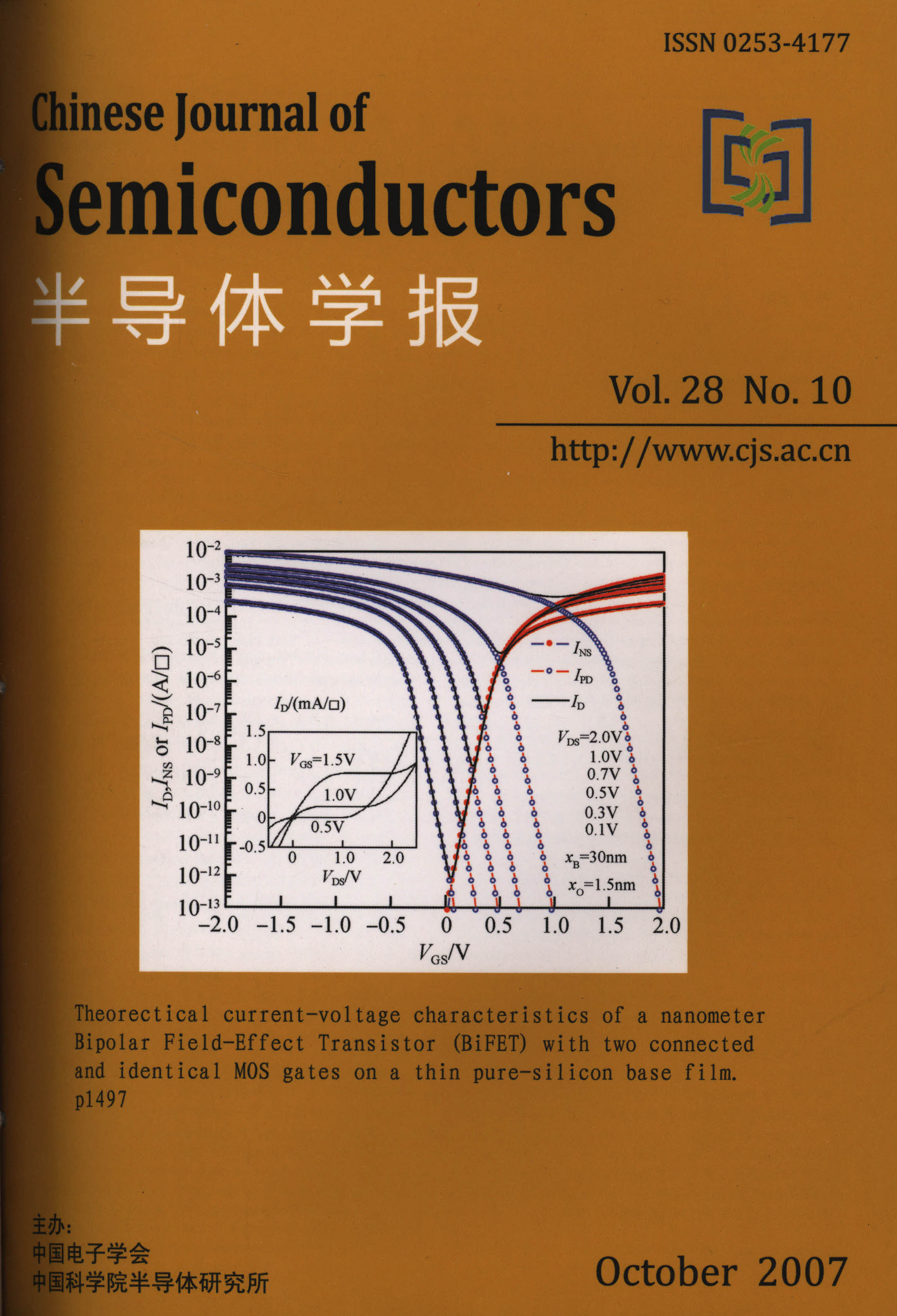
2007, 28(10): 1497-1502
Abstract PDF

The bipolar theory of fieldeffect transistor is introduced to replace the 55-year-old classic unipolar theory invented by Shockley in 1952 in order to account for the characteristics observed in recent double-gate nanometer silicon MOS field-effect transistors.Two electron and two hole surface channels are simultaneously present in all channel current ranges.Output and transfer characteristics are computed over practical base and gate oxide thicknesses.The bipolar theory corroborates well with experimental data reported recently for FinFETs with metal/silicon and p/n junction source/drain contacts.Singledevice realization of CMOS inverter and SRAM memory circuit functions are recognized.

The bipolar theory of fieldeffect transistor is introduced to replace the 55-year-old classic unipolar theory invented by Shockley in 1952 in order to account for the characteristics observed in recent double-gate nanometer silicon MOS field-effect transistors.Two electron and two hole surface channels are simultaneously present in all channel current ranges.Output and transfer characteristics are computed over practical base and gate oxide thicknesses.The bipolar theory corroborates well with experimental data reported recently for FinFETs with metal/silicon and p/n junction source/drain contacts.Singledevice realization of CMOS inverter and SRAM memory circuit functions are recognized.
Low Temperature Synthesis and Optical Properties of ZnO Nanowires
Chang Peng, Liu Su, Chen Rongbo, Tang Ying, Han Genliang
Chin. J. Semicond.  2007, 28(10): 1503-1507
Abstract PDF

ZnO nanowire arrays are fabricated on anodized aluminum oxide templates with electric field-assisted electrochemical technology.Transmission electron microscopy results indicate that the nanowires are straight and uniform.X-ray diffraction patterns indicate that the nanowires are highly oriented.The result of selected area electron diffraction suggests that the nanowires are single crystals.The photoluminescence spectrum presents a broad-band luminescence in the region of 350~650nm.The effect of the assisted transverse electric field on the growth process of ZnO nanowires is also discussed.

ZnO nanowire arrays are fabricated on anodized aluminum oxide templates with electric field-assisted electrochemical technology.Transmission electron microscopy results indicate that the nanowires are straight and uniform.X-ray diffraction patterns indicate that the nanowires are highly oriented.The result of selected area electron diffraction suggests that the nanowires are single crystals.The photoluminescence spectrum presents a broad-band luminescence in the region of 350~650nm.The effect of the assisted transverse electric field on the growth process of ZnO nanowires is also discussed.
Growth of Free-Standing AlN Nanocrystals on Nanorod ZnO Template
Hu Weiguo, Wei Hongyuan, Jiao Chunmei, Kang Tingting, Zhang Riqing, Liu Xianglin
Chin. J. Semicond.  2007, 28(10): 1508-1512
Abstract PDF

AlN film is deposited on a nanorod ZnO template by metalorganic chemical vapor deposition.Scanning electron microscopy measurements reveal that this film forms a lying nanorod surface.The grazing incidence X-ray diffraction further proves that it is entirely a wurtzite AlN structure,and the average size of the crystallite grains is about 12nm,which is near the ZnO nanorod diameter (30nm).This means that the nanorod ZnO template can restrict the AlN lateral overgrowth.Additionally,by etching the ZnO template with H2 at high temperatures,we directly achieve epitaxial lift-off during the growth process.Eventually,free-standing AlN nanocrystals are achieved,and the undamaged area is near 1cm×1cm.We define the growth mechanism as a "grow-etch-merge" process.

AlN film is deposited on a nanorod ZnO template by metalorganic chemical vapor deposition.Scanning electron microscopy measurements reveal that this film forms a lying nanorod surface.The grazing incidence X-ray diffraction further proves that it is entirely a wurtzite AlN structure,and the average size of the crystallite grains is about 12nm,which is near the ZnO nanorod diameter (30nm).This means that the nanorod ZnO template can restrict the AlN lateral overgrowth.Additionally,by etching the ZnO template with H2 at high temperatures,we directly achieve epitaxial lift-off during the growth process.Eventually,free-standing AlN nanocrystals are achieved,and the undamaged area is near 1cm×1cm.We define the growth mechanism as a "grow-etch-merge" process.
A Ka-Band PHEMT MMIC 1W Power Amplifier
Yu Mengxia, Li Aibin, Xu Jun
Chin. J. Semicond.  2007, 28(10): 1513-1517
Abstract PDF

The performance of a microwave monolithic integrated circuit (MMIC) amplifier with high output power in the Ka-band is presented.Using 75mm 0.25μm GaAs PHEMT technology provided by the Hebei Semiconductor Research Institute,this three-stage power amplifier,with a chip size of 19.25mm2(3.5mm×5.5mm),on 100μm GaAs substrate achieves a linear gain of more than 16dB in the 32.5~35.5GHz frequency range,with an average output power at 1dB gain compression of P1dB=29.8dBm and a maximum saturated output power of Psat=31dBm.

The performance of a microwave monolithic integrated circuit (MMIC) amplifier with high output power in the Ka-band is presented.Using 75mm 0.25μm GaAs PHEMT technology provided by the Hebei Semiconductor Research Institute,this three-stage power amplifier,with a chip size of 19.25mm2(3.5mm×5.5mm),on 100μm GaAs substrate achieves a linear gain of more than 16dB in the 32.5~35.5GHz frequency range,with an average output power at 1dB gain compression of P1dB=29.8dBm and a maximum saturated output power of Psat=31dBm.
PAPERS
Fabrication and Characterization of Strained Si Material Using SiGe Virtual Substrate for High Mobility Devices
Liang Renrong, Zhang Kan, Yang Zongren, Xu Yang, Wang Jing, Xu Jun
Chin. J. Semicond.  2007, 28(10): 1518-1522
Abstract PDF

The fabrication and characterization of strained-Si material grown on a relaxed Si0.79Ge0.21/graded Si1-xGex/Si virtual substrate,using reduced pressure chemical vapor deposition,are presented.The Ge concentration of the constant composition SiGe layer and the grading rate of the graded SiGe layer are estimated with double-crystal X-ray diffraction and further confirmed by SIMS measurements.The surface root mean square roughness of the strained Si cap layer is 2.36nm,and the strain is about 0.83% as determined by atomic force microscopy and Raman spectra,respectively.The threading dislocation density is on the order of 4e4cm-2.Furthermore,it is found that the stress in the strained Si cap layer is maintained even after the high thermal budget process.nMOSFET devices are fabricated and measured in strained-Si and unstrained bulk-Si channels.Compared to the co-processed bulk-Si MOSFETs at room temperature,a significant low vertical field mobility enhancement of about 85% is observed in the strained-Si devices.

The fabrication and characterization of strained-Si material grown on a relaxed Si0.79Ge0.21/graded Si1-xGex/Si virtual substrate,using reduced pressure chemical vapor deposition,are presented.The Ge concentration of the constant composition SiGe layer and the grading rate of the graded SiGe layer are estimated with double-crystal X-ray diffraction and further confirmed by SIMS measurements.The surface root mean square roughness of the strained Si cap layer is 2.36nm,and the strain is about 0.83% as determined by atomic force microscopy and Raman spectra,respectively.The threading dislocation density is on the order of 4e4cm-2.Furthermore,it is found that the stress in the strained Si cap layer is maintained even after the high thermal budget process.nMOSFET devices are fabricated and measured in strained-Si and unstrained bulk-Si channels.Compared to the co-processed bulk-Si MOSFETs at room temperature,a significant low vertical field mobility enhancement of about 85% is observed in the strained-Si devices.
Circuit-Level Analysis on Opto-Electronic Characteristics of Ferroelectric Liquid Crystal
Zhu Siqi
Chin. J. Semicond.  2007, 28(10): 1523-1526
Abstract PDF

We propose an electronic model in Spice,instead of traditional mathematical analysis,for analyzing the performance of ferroelectric liquid crystal (FLC) under various working conditions.Using this equivalent circuit model,it is easy to simulate and analyze the behavior of an FLC layer in three different typical parameters,including temperature,input light wavelength,and the frequency of driving voltage.We conclude that the response velocity drops as the wavelength increases in the range of visible light,and for the parameter of temperature,the velocity reaches its lowest value when the temperature reaches a certain degree;meanwhile,the frequency of driving voltage exerts important effects on the response velocity only when the frequency is beyond a critical value.Excellent agreement is achieved between simulation and experimental results.

We propose an electronic model in Spice,instead of traditional mathematical analysis,for analyzing the performance of ferroelectric liquid crystal (FLC) under various working conditions.Using this equivalent circuit model,it is easy to simulate and analyze the behavior of an FLC layer in three different typical parameters,including temperature,input light wavelength,and the frequency of driving voltage.We conclude that the response velocity drops as the wavelength increases in the range of visible light,and for the parameter of temperature,the velocity reaches its lowest value when the temperature reaches a certain degree;meanwhile,the frequency of driving voltage exerts important effects on the response velocity only when the frequency is beyond a critical value.Excellent agreement is achieved between simulation and experimental results.
Multi-Finger Power SiGe HBT with Non-Uniform Finger Spacing
Jin Dongyue, Zhang Wanrong, Shen Pei, Xie Hongyun, Wang Yang
Chin. J. Semicond.  2007, 28(10): 1527-1531
Abstract PDF

A multi-finger power SiGe heterojunction bipolar transistor (HBT) with non-uniform finger spacing was fabricated to improve thermal stability.Experimental results show that the peak temperature is reduced by 22K compared with that of an HBT with uniform finger spacing in the same operating conditions.The temperature profile across the device can be improved at different biases for the same HBT with non-uniform finger spacing.Because of the decrease in peak temperature and the improvement of temperature profile,the power SiGe HBT with non-uniform spacing can operate at higher bias and hence has higher power handling capability.

A multi-finger power SiGe heterojunction bipolar transistor (HBT) with non-uniform finger spacing was fabricated to improve thermal stability.Experimental results show that the peak temperature is reduced by 22K compared with that of an HBT with uniform finger spacing in the same operating conditions.The temperature profile across the device can be improved at different biases for the same HBT with non-uniform finger spacing.Because of the decrease in peak temperature and the improvement of temperature profile,the power SiGe HBT with non-uniform spacing can operate at higher bias and hence has higher power handling capability.
Dual-Work-Function Ni-FUSI Metal Gate for CMOS Technology
Zhou Huajie, Xu Qiuxia
Chin. J. Semicond.  2007, 28(10): 1532-1539
Abstract PDF

This paper investigates the work function adjustment of a full silicidation (Ni-FUSI) metal gate.It is found that implanting dopant into poly-Si before silicidation can modulate the work function of a Ni-FUSI metal gate efficiently.With the implantation of p-type or n-type dopants,such as BF2,As,and P,the work function of a Ni-FUSI metal gate can be made higher or lower to satisfy the requirement of pMOS or nMOS,respectively.But implanting a high dose of As into a poly-Si gate before silicidation will cause the delamination effect and EOT loss,and thus As dopant is not suitable to be used to adjust the work function of a Ni-FUSI metal gate.Due to the EOT reduction in the FUSI process,the gate leakage current of a FUSI metal gate capacitor is larger than that of a poly-Si gate capacitor.

This paper investigates the work function adjustment of a full silicidation (Ni-FUSI) metal gate.It is found that implanting dopant into poly-Si before silicidation can modulate the work function of a Ni-FUSI metal gate efficiently.With the implantation of p-type or n-type dopants,such as BF2,As,and P,the work function of a Ni-FUSI metal gate can be made higher or lower to satisfy the requirement of pMOS or nMOS,respectively.But implanting a high dose of As into a poly-Si gate before silicidation will cause the delamination effect and EOT loss,and thus As dopant is not suitable to be used to adjust the work function of a Ni-FUSI metal gate.Due to the EOT reduction in the FUSI process,the gate leakage current of a FUSI metal gate capacitor is larger than that of a poly-Si gate capacitor.
A 10bit 2GHz CMOS D/A Converter for High-Speed System Applications
Yuan Ling, Ni Weining, Shi Yin
Chin. J. Semicond.  2007, 28(10): 1540-1545
Abstract PDF

This paper presents a 2GS/s 10bit CMOS digital-to-analog converter (DAC) that consists of two unit current-cell matrixes for 6MSBs and 4LSBs,respectively,trading off between the precision and size of the chip.Current mode logic (CML) is used to ensure high speed,and a double centro-symmetric current matrix is designed by the Q2 random walk strategy in order to ensure the linearity of the DAC.The DAC occupies 2.2mm×2.2mm of die area and consumes 790mW with a single 3.3V power supply.

This paper presents a 2GS/s 10bit CMOS digital-to-analog converter (DAC) that consists of two unit current-cell matrixes for 6MSBs and 4LSBs,respectively,trading off between the precision and size of the chip.Current mode logic (CML) is used to ensure high speed,and a double centro-symmetric current matrix is designed by the Q2 random walk strategy in order to ensure the linearity of the DAC.The DAC occupies 2.2mm×2.2mm of die area and consumes 790mW with a single 3.3V power supply.
A Novel CMOS Voltage Reference Based on Threshold Voltage Difference Between p-Type and n-Type MOSFETs
Kong Ming, Guo Jianmin, Zhang Ke, Li Wenhong
Chin. J. Semicond.  2007, 28(10): 1546-1550
Abstract PDF

A novel MOS-only voltage reference is presented,which is based on the threshold voltage difference between p-type and n-type MOSFETs.Its precision is improved by the cancellation of the process variation.The reference has been successfully implemented in a Chartered 0.35μm CMOS process.The occupied chip area is 0.022mm2.Measurements indicate that without trimming,the average output voltage error is 6mV at room temperature compared with the simulation result.The temperature coefficient is 180ppm/℃ in the worst case in the temperature range of 0 to 100℃,and the line regulation is ±1.1%.The reference is applied in an adaptive power MOSFET driver.

A novel MOS-only voltage reference is presented,which is based on the threshold voltage difference between p-type and n-type MOSFETs.Its precision is improved by the cancellation of the process variation.The reference has been successfully implemented in a Chartered 0.35μm CMOS process.The occupied chip area is 0.022mm2.Measurements indicate that without trimming,the average output voltage error is 6mV at room temperature compared with the simulation result.The temperature coefficient is 180ppm/℃ in the worst case in the temperature range of 0 to 100℃,and the line regulation is ±1.1%.The reference is applied in an adaptive power MOSFET driver.
Elastic-Plastic Mechanical Properties of AlxGa1-xN Thin Films with High Al Composition
Xu Fujun, Shen Bo, Wang Maojun, Xu jian, Miao Zhenlin, Yang Zhijian, Qin Zhixin, Zhang Guoyi, Lin Bing, Bai Shulin
Chin. J. Semicond.  2007, 28(10): 1551-1554
Abstract PDF

The elastic-plastic mechanical properties of AlxGa1-xN thin films with high Al composition are investigated by the nano-indentation technique.It is found that the Young’s modulus E of the films and the shear stress to produce the plastic deformation in AlxGa1-xN films increase with increasing Al composition,while the occurrence of the clear and sudden displacement discontinuity ( "pop-in" ) in the plastic deformation (PD) process decreases.With increasing Al composition,it is believed that the increase of the bond strength and the decrease of the stress due to the lesser lattice mismatch between AlxGa1-xN films and AlN/sapphire templates result in more resistance to the formation of dislocations,which is responsible for the "pop-in" behavior in AlxGa1-xN films.

The elastic-plastic mechanical properties of AlxGa1-xN thin films with high Al composition are investigated by the nano-indentation technique.It is found that the Young’s modulus E of the films and the shear stress to produce the plastic deformation in AlxGa1-xN films increase with increasing Al composition,while the occurrence of the clear and sudden displacement discontinuity ( "pop-in" ) in the plastic deformation (PD) process decreases.With increasing Al composition,it is believed that the increase of the bond strength and the decrease of the stress due to the lesser lattice mismatch between AlxGa1-xN films and AlN/sapphire templates result in more resistance to the formation of dislocations,which is responsible for the "pop-in" behavior in AlxGa1-xN films.
First-Principles Calculation of Electronic Structure and Optical Properties of Anatase TiO2
Zhao Zongyan, Liu Qingju, Zhu Zhongqi, Zhang Jin
Chin. J. Semicond.  2007, 28(10): 1555-1561
Abstract PDF

A first-principle calculation using the plane-wave ultrasoft pseudopotential method is performed to investigate the electronic structure and optical properties of anatase TiO2 in detail,and their relationship is theoretically analyzed.The dielectric function and complex refractive,reflectivity,and absorption coefficients of anatase TiO2 dominated by electron interband transitions are analyzed in terms of the precisely calculated band structure and density of states.The theoretical results agree well with the experimental data and show significant optical anisotropy in the polarization direction of E∥c and E⊥c,offering a theoretical basis for the application of anatase TiO2.

A first-principle calculation using the plane-wave ultrasoft pseudopotential method is performed to investigate the electronic structure and optical properties of anatase TiO2 in detail,and their relationship is theoretically analyzed.The dielectric function and complex refractive,reflectivity,and absorption coefficients of anatase TiO2 dominated by electron interband transitions are analyzed in terms of the precisely calculated band structure and density of states.The theoretical results agree well with the experimental data and show significant optical anisotropy in the polarization direction of E∥c and E⊥c,offering a theoretical basis for the application of anatase TiO2.
Growth and Stress Analysis of a-Plane GaN Films Grown on r-Plane Sapphire Substrate with a Two-Step AlN Buffer Layer
Yan Jianfeng, Zhang Jie, Guo Liwei, Zhu Xueliang, Peng Mingzeng, Jia Haiqiang, Chen Hong, Zhou Junming
Chin. J. Semicond.  2007, 28(10): 1562-1567
Abstract PDF

a-plane GaN films were grown on r-plane sapphire substrates by metalorganic chemical vapor deposition with a two-step AlN buffer layer.High-resolution X-ray diffraction and micro-Raman scattering were used to analyze the residual strain and crystalline quality of the as-grown samples.The on-axis full width at half maximum value (FWHM) of the X-ray rocking curve is 0.193°,and the FWHM of the E2 -high energy peak is 3.9cm-1,indicating that the as-grown sample is of high quality.The orientation of the a-plane GaN with respect to r-plane sapphire substrate is confirmed to be [1120]GaN‖[1102]sapphire,[0001]GaN‖[1101]sapphire and [1100]GaN‖[1120]sapphire.The residual stress of the a-plane GaN grown with two-step AlN buffer is different from that of thea-plane GaN grown with a low-temperature GaN buffer,due to the effects of the AlN buffer,which has a larger thermal mismatch to sapphire than that of GaN.

a-plane GaN films were grown on r-plane sapphire substrates by metalorganic chemical vapor deposition with a two-step AlN buffer layer.High-resolution X-ray diffraction and micro-Raman scattering were used to analyze the residual strain and crystalline quality of the as-grown samples.The on-axis full width at half maximum value (FWHM) of the X-ray rocking curve is 0.193°,and the FWHM of the E2 -high energy peak is 3.9cm-1,indicating that the as-grown sample is of high quality.The orientation of the a-plane GaN with respect to r-plane sapphire substrate is confirmed to be [1120]GaN‖[1102]sapphire,[0001]GaN‖[1101]sapphire and [1100]GaN‖[1120]sapphire.The residual stress of the a-plane GaN grown with two-step AlN buffer is different from that of thea-plane GaN grown with a low-temperature GaN buffer,due to the effects of the AlN buffer,which has a larger thermal mismatch to sapphire than that of GaN.
Epitaxial Growth of Atomically Flat AlN Layers on Sapphire Substrate by Metal Organic Chemical Vapor Deposition
Zhao Hong, Zou Zeya, Zhao Wenbai, Liu Ting, Yang Xiaobo, Liao Xiuying, Wang Zhen, Zhou Yong, Liu Wanqing
Chin. J. Semicond.  2007, 28(10): 1568-1573
Abstract PDF

AlN layers were grown on sapphire substrate by metal organic chemical vapor deposition (MOCVD) at 1200℃,5kPa.Atomically flat epilayers were obtained at a low V/III flow ratio without nitridation on the substrate.Atomic force microscopy (AFM) reveals a roughness of around 0.44nm for the atomically flat layers with an FWHM of (0002) X-ray diffraction rocking curve around 166" .Analysis of the growth results demonstrates that the polarity of the AlN layer and vapor phase reaction between NH3 and the Al-precursor are the primary factors affecting the AlN surface morphology.High quality n-doped AlGaN layers with high Al content were obtained using the as-grown atomically flat AlN layers,implying the good quality of the layers as epitaxial template.

AlN layers were grown on sapphire substrate by metal organic chemical vapor deposition (MOCVD) at 1200℃,5kPa.Atomically flat epilayers were obtained at a low V/III flow ratio without nitridation on the substrate.Atomic force microscopy (AFM) reveals a roughness of around 0.44nm for the atomically flat layers with an FWHM of (0002) X-ray diffraction rocking curve around 166" .Analysis of the growth results demonstrates that the polarity of the AlN layer and vapor phase reaction between NH3 and the Al-precursor are the primary factors affecting the AlN surface morphology.High quality n-doped AlGaN layers with high Al content were obtained using the as-grown atomically flat AlN layers,implying the good quality of the layers as epitaxial template.
Basis Mechanism of MIC Poly-Si Thin Film Material Dynamic Gettered Technology and Its Applications
Li Yang, Meng Zhiguo, Wu Chunya, Wong M, Kwok H S, Zhang Fang, Xiong Shaozhen
Chin. J. Semicond.  2007, 28(10): 1574-1579
Abstract PDF

The basis mechanism and main process flow of metal induced crystallization poly-Si (MIC poly-Si) dynamic gettering are discussed,and its applications are studied for use in poly-Si thin film transistor devices.In the research of MIC poly-Si and producing TFT with poly-Si as the active layer,we find that nickel residue is left in the MIC poly-Si thin film,and the amount of nickel is extremely high along the grain boundary.This can reduce the stability and reliability of the TFT as well as the whole system.In order to improve the performance of MIC thin films and devices,we use dynamic nickel gettering by phosphor-silicate glass (PSG) to absorb nickel effectively,reducing the residual nickel in the poly-Si,reducing the number of defects at the conflicting crystal boundaries,and decreasing the leakage current of the TFT.The simple process flow and low cost make it suitable for industrial manufacturing.This is a necessary step in the production of microelectronics devices and systems.

The basis mechanism and main process flow of metal induced crystallization poly-Si (MIC poly-Si) dynamic gettering are discussed,and its applications are studied for use in poly-Si thin film transistor devices.In the research of MIC poly-Si and producing TFT with poly-Si as the active layer,we find that nickel residue is left in the MIC poly-Si thin film,and the amount of nickel is extremely high along the grain boundary.This can reduce the stability and reliability of the TFT as well as the whole system.In order to improve the performance of MIC thin films and devices,we use dynamic nickel gettering by phosphor-silicate glass (PSG) to absorb nickel effectively,reducing the residual nickel in the poly-Si,reducing the number of defects at the conflicting crystal boundaries,and decreasing the leakage current of the TFT.The simple process flow and low cost make it suitable for industrial manufacturing.This is a necessary step in the production of microelectronics devices and systems.
Quantum Circuit Equation and Quantum Current of Mesoscopic Electron Resonator with Charge Discreteness
Cui Yuanshun
Chin. J. Semicond.  2007, 28(10): 1580-1583
Abstract PDF

On the basis of charge discreteness,the properties of quantum current in a mesoscopic electron resonator are investigated by the minimum shift operator.Quantum Kirchhoff’s equation,the current relation,and the fluctuations of current are given.The results show that when charge quantization is taken into account,the charge in the resonator has the characteristic of quantum vibration;the quantum current and the fluctuation are related to the charge quantum and Planck constant,respectively,and the size is determined by the self-inductance of the system.

On the basis of charge discreteness,the properties of quantum current in a mesoscopic electron resonator are investigated by the minimum shift operator.Quantum Kirchhoff’s equation,the current relation,and the fluctuations of current are given.The results show that when charge quantization is taken into account,the charge in the resonator has the characteristic of quantum vibration;the quantum current and the fluctuation are related to the charge quantum and Planck constant,respectively,and the size is determined by the self-inductance of the system.
Electrical Structures of Nitrogen-Doped Zigzag Single-Wall Carbon Nanotubes
Song Jiuxu, Yang Yintang, Chai Changchun, Li Yuejin
Chin. J. Semicond.  2007, 28(10): 1584-1588
Abstract PDF

Based on the study of the existing form of doped single-walled carbon nanotubes (SWCNT) and the optimization of SWCNT crystal lattice,the band structure and density of states of nitrogen-doped SWCNTs are studied.We take a first-principle ultra-soft pseudopotential approach using plane waves that is based upon density functional theory,and use the CASTEP program package.The results show that the band gap narrows with the increase of nitrogen doping concentration

Based on the study of the existing form of doped single-walled carbon nanotubes (SWCNT) and the optimization of SWCNT crystal lattice,the band structure and density of states of nitrogen-doped SWCNTs are studied.We take a first-principle ultra-soft pseudopotential approach using plane waves that is based upon density functional theory,and use the CASTEP program package.The results show that the band gap narrows with the increase of nitrogen doping concentration
Effects of Surface-Modified Gate Dielectrics on Electrical Characteristics of Organic Thin-Film Transistors
Chen Ling, Zhu Wenqing, Bai Yu, Liu Xiang, Jiang Xueyin, Zhang Zhilin
Chin. J. Semicond.  2007, 28(10): 1589-1593
Abstract PDF

Organic thin film transistors (OTFTs) with a modified gate insulator are demonstrated.The modified gate insulator layers consist of SiO2 as the gate insulator and OTS (octadecyltrichlorosilane) or PMMA (poly methyl methacylate) as the modified layer.The devices with the modified layer have a field-effect mobility larger than 1e-3cm2/(V·s) and an on/off current ratio greater than 1e4,while their leakage current is decreased to 1e-10A.The results demonstrate that using modified gate insulators is an effective method to fabricate OTFTs with improved electric characteristics.

Organic thin film transistors (OTFTs) with a modified gate insulator are demonstrated.The modified gate insulator layers consist of SiO2 as the gate insulator and OTS (octadecyltrichlorosilane) or PMMA (poly methyl methacylate) as the modified layer.The devices with the modified layer have a field-effect mobility larger than 1e-3cm2/(V·s) and an on/off current ratio greater than 1e4,while their leakage current is decreased to 1e-10A.The results demonstrate that using modified gate insulators is an effective method to fabricate OTFTs with improved electric characteristics.
Design and Fabrication of Resonant Tunneling Transistor with RTD/HEMT in Series Structure
Liang Huilai, Guo Weilian, Song Ruiliang, Qi Haitao, Zhang Shilin, Hu Liuchang, Li Jianheng, Mao Luhong, Shang Yuehui, Feng Zhen, Tian Guoping, Li Yali
Chin. J. Semicond.  2007, 28(10): 1594-1598
Abstract PDF

The design and fabrication of a resonant tunneling transistor with an RTD/HEMT in-series structure are presented.The measurement results of the fabricated devices show that the maximum peak valley current ratio (PVCR) is 17.6∶1,the gate voltage modulating peak voltage ratio is in the range of 1.5~7.7,and the -3dB cut-off frequency is about 4GHz.This device is compatible with HEMTs in the device structure and fabrication technology,and can be used in high speed circuits with HEMTs devices.

The design and fabrication of a resonant tunneling transistor with an RTD/HEMT in-series structure are presented.The measurement results of the fabricated devices show that the maximum peak valley current ratio (PVCR) is 17.6∶1,the gate voltage modulating peak voltage ratio is in the range of 1.5~7.7,and the -3dB cut-off frequency is about 4GHz.This device is compatible with HEMTs in the device structure and fabrication technology,and can be used in high speed circuits with HEMTs devices.
Low-Energy Proton Irradiation Effects of GaInP/GaAs/Ge Triple-Junction Solar Cells for Space Use
Wang Rong, Liu Yunhong, Sun Xufang, Cui Xinyu
Chin. J. Semicond.  2007, 28(10): 1599-1602
Abstract PDF

GaInP/GaAs/Ge triple-junction (3J) solar cells fabricated by metal-organic chemical vapor deposition were irradiated with 0.28,0.62,and 2.80MeV protons at doses ranging from 1e10 to 1e13cm-2 using a 2×1.7MV tandem accelerator.The performance degradation of the 3J solar cells was analyzed with current-voltage characteristics and spectral response measurements.The degradation rates of the short circuit current (Isc),open circuit voltage (Voc),and maximum power output (Pmax) were found to increase as the proton irradiation dose increased,but the degradation rates of Isc,Voc,and Pmax decreased as the proton irradiation energy increased.Irradiation with a proton energy of 0.28MeV gave rise to the highest degradation rates of Isc,Voc,and Pmax of the solar cells.Also,the spectral response of the GaAs middle cell in 3J solar cells was degraded more significantly than the GaInP top cell.

GaInP/GaAs/Ge triple-junction (3J) solar cells fabricated by metal-organic chemical vapor deposition were irradiated with 0.28,0.62,and 2.80MeV protons at doses ranging from 1e10 to 1e13cm-2 using a 2×1.7MV tandem accelerator.The performance degradation of the 3J solar cells was analyzed with current-voltage characteristics and spectral response measurements.The degradation rates of the short circuit current (Isc),open circuit voltage (Voc),and maximum power output (Pmax) were found to increase as the proton irradiation dose increased,but the degradation rates of Isc,Voc,and Pmax decreased as the proton irradiation energy increased.Irradiation with a proton energy of 0.28MeV gave rise to the highest degradation rates of Isc,Voc,and Pmax of the solar cells.Also,the spectral response of the GaAs middle cell in 3J solar cells was degraded more significantly than the GaInP top cell.
A White OLED with Liq∶Rubrene as Emitting Layer
Wu Youyu, Tu Kexu, Li Hairong, Ou Guping, Zhang Fujia, Yang Aiguo
Chin. J. Semicond.  2007, 28(10): 1603-1606
Abstract PDF

A novel white organic light emitting device with a single layer consisting of an orange-red dopant 5,6,11,12-tetraphenylnaphthacene (Rubrene) and a blue light emitting material 8-hydroxyquinoline lithium (Liq) mixed in a certain proportion was fabricated.When the proportion is 1.1%,the commission international De L’Eclairage (CIE) coordinate of the device is (0.308,0.347).The driving voltage of the device is 8V,and the luminescence brightness is 3120cd/m2 when the voltage is increased to 25V.

A novel white organic light emitting device with a single layer consisting of an orange-red dopant 5,6,11,12-tetraphenylnaphthacene (Rubrene) and a blue light emitting material 8-hydroxyquinoline lithium (Liq) mixed in a certain proportion was fabricated.When the proportion is 1.1%,the commission international De L’Eclairage (CIE) coordinate of the device is (0.308,0.347).The driving voltage of the device is 8V,and the luminescence brightness is 3120cd/m2 when the voltage is increased to 25V.
A Single Fiber Coupling Technique for High Power Diode Laser Arrays
Niu Gang, Fan Zhongwei, Wang Peifeng, Cui Jianfeng, Shi Zhaohui, Zhang Jing
Chin. J. Semicond.  2007, 28(10): 1607-1610
Abstract PDF

This paper reports two pairs of laser diode arrays (LDA) with wavelengths of 808 and 980nm,respectively,whose beams were mixed into a single fiber using step-mirror beam-shaping technology,polarization,and wavelength coupling technology.As a result,a single fiber optic coupling module of LDA was achieved,of which the output power is 95.8W,maximal coupling efficiency is more than 60%,the diameter of the fiber core is 400μm,and NA is 0.22

This paper reports two pairs of laser diode arrays (LDA) with wavelengths of 808 and 980nm,respectively,whose beams were mixed into a single fiber using step-mirror beam-shaping technology,polarization,and wavelength coupling technology.As a result,a single fiber optic coupling module of LDA was achieved,of which the output power is 95.8W,maximal coupling efficiency is more than 60%,the diameter of the fiber core is 400μm,and NA is 0.22
Effect of Power on Property of Plasma in Polysilicon Gate over Etch Process
Zhang Qingzhao, Xie Changqing, Liu Ming, Li Bing, Zhu Xiaoli
Chin. J. Semicond.  2007, 28(10): 1611-1614
Abstract PDF

The relations between the parameters of plasma and those of RF power and gas flow were analyzed under the conditions of over etch step in semiconductor plasma etching,by Langmuir probe.The results show that as the RF power was increasing,the RF couple coefficient was comparatively stable.When in a local heating state,most of the electrons were in an adhesive status.The distribution of power couple space in the chamber can be improved as the RF power increases.These results can help to develop plasma dry etching.

The relations between the parameters of plasma and those of RF power and gas flow were analyzed under the conditions of over etch step in semiconductor plasma etching,by Langmuir probe.The results show that as the RF power was increasing,the RF couple coefficient was comparatively stable.When in a local heating state,most of the electrons were in an adhesive status.The distribution of power couple space in the chamber can be improved as the RF power increases.These results can help to develop plasma dry etching.
Etching Si Wafer Using Atmospheric Pressure RF Cold Plasma Jet
Zhao Lingli, Duan Xiaojin, Yin Minghui, Xu Xiangyu, Wang Shouguo
Chin. J. Semicond.  2007, 28(10): 1615-1619
Abstract PDF

A new kind of discharging device with a RF cold plasma jet at atmospheric pressure is introduced,and it is utilized to conduct experimental research on silicon-etching.The characteristics of the etching rate depend on the input power,gas flow,and temperature of Si wafers.The maximal etching rate is 390nm/min.The etching effect is characterized by step instrument,optical microscopy,and SEM.Excellent etching homogeneity and satisfactory anisotropy can be obtained during material etching with this device.These results indicate that the silicon-etching operation with this atmospheric pressure device is simple and causes no material surface damage.

A new kind of discharging device with a RF cold plasma jet at atmospheric pressure is introduced,and it is utilized to conduct experimental research on silicon-etching.The characteristics of the etching rate depend on the input power,gas flow,and temperature of Si wafers.The maximal etching rate is 390nm/min.The etching effect is characterized by step instrument,optical microscopy,and SEM.Excellent etching homogeneity and satisfactory anisotropy can be obtained during material etching with this device.These results indicate that the silicon-etching operation with this atmospheric pressure device is simple and causes no material surface damage.
A Highly Symmetrical Capacitive Accelerometer by Silicon Four-Layer Bonding
Xu Weihe, Che Lufeng, Li Yufang, Xiong Bin, Wang Yuelin
Chin. J. Semicond.  2007, 28(10): 1620-1624
Abstract PDF

This paper presents a highly symmetrical capacitive accelerometer fabricated by four silicon wafers bonded together.The cantilever-mass structure is fabricated by bonding two wafers together by silicon fusion,and the two static electrodes are bonded later by low-temperature glass melting.Through the silicon bonding,we achieve a wafer-level vacuum package,and the wire-bonding PAD is made after the fabrication is complete.The dimensions of the chip are 6.8mm×5.6mm×1.68mm,and those of the mass are 3.2mm×3.2mm×0.84mm.The test results of the sensor show that the sensitivity is about 6pF/g,the Q value is 35,the resonant frequency is 489Hz,and the leakage is less than 0.1e-9cm3/s.

This paper presents a highly symmetrical capacitive accelerometer fabricated by four silicon wafers bonded together.The cantilever-mass structure is fabricated by bonding two wafers together by silicon fusion,and the two static electrodes are bonded later by low-temperature glass melting.Through the silicon bonding,we achieve a wafer-level vacuum package,and the wire-bonding PAD is made after the fabrication is complete.The dimensions of the chip are 6.8mm×5.6mm×1.68mm,and those of the mass are 3.2mm×3.2mm×0.84mm.The test results of the sensor show that the sensitivity is about 6pF/g,the Q value is 35,the resonant frequency is 489Hz,and the leakage is less than 0.1e-9cm3/s.
Fabricating High Performance Diffractive Microlens by Single Step Photolithography and Wet Etching
Zhang Xinyu, Chen Shengbin, Ji An, Xie Changsheng
Chin. J. Semicond.  2007, 28(10): 1625-1629
Abstract PDF

We discuss a low cost fabrication method of a diffractive microlens with high performance for both blue and red DVD objective lenses,which consists of single-step photolithography and a wet etching process.The surface roughness of the fabricated micro-optics structure is in the nanometer range;The feature height of the diffractive phase step is in the sub-micrometer range;And can be adjusted according to requirements;And the optical aperture of the microlens can be changed from millimeter to centimeter magnitude.A large number of basic phase structures in the diffractive microlens can be set and arranged by a diffractive integrating algorithm according to the appearance and feature parameters of the beam process.Far field optical measurement shows a high diffractive efficiency of the fabricated diffractive structure.

We discuss a low cost fabrication method of a diffractive microlens with high performance for both blue and red DVD objective lenses,which consists of single-step photolithography and a wet etching process.The surface roughness of the fabricated micro-optics structure is in the nanometer range;The feature height of the diffractive phase step is in the sub-micrometer range;And can be adjusted according to requirements;And the optical aperture of the microlens can be changed from millimeter to centimeter magnitude.A large number of basic phase structures in the diffractive microlens can be set and arranged by a diffractive integrating algorithm according to the appearance and feature parameters of the beam process.Far field optical measurement shows a high diffractive efficiency of the fabricated diffractive structure.
A Novel Micromachined x-Axis Tuning Fork Gyroscope Based on "8-Beams/Proofmass" Structure
Duan Fei, Jiao Jiwei, Wang Yucai, Zhang Ying, Mi Binwei, Li Jinpeng, Qian Qing, Wang Yuelin
Chin. J. Semicond.  2007, 28(10): 1630-1635
Abstract PDF

A novel x-axis tuning fork MEMS gyroscope with "8-beams/proofmass" structure for detecting the Coriolis effect is presented.Compared with the common single-plane beams,the 8 vertical beams,symmetrically located at the top and bottom sides,more stably suspend the large thick proof mass,resulting in large capacitance variation and low mechanical noise.Bulk-micromachining technology is applied to obtain the large proof mass and twin dual beams.During the fabrication process,the dimensions of the beams are precisely confined by thermal oxide-protected limit trench sidewalls and the extremely slowly etched (111)-planes;therefore a small mismatch of less than 30Hz is achieved before tuning.Initial testing shows a sensitivity of 0.15mV/(°/s) and a rate resolution around 0.1°/s under atmosphere pressure.

A novel x-axis tuning fork MEMS gyroscope with "8-beams/proofmass" structure for detecting the Coriolis effect is presented.Compared with the common single-plane beams,the 8 vertical beams,symmetrically located at the top and bottom sides,more stably suspend the large thick proof mass,resulting in large capacitance variation and low mechanical noise.Bulk-micromachining technology is applied to obtain the large proof mass and twin dual beams.During the fabrication process,the dimensions of the beams are precisely confined by thermal oxide-protected limit trench sidewalls and the extremely slowly etched (111)-planes;therefore a small mismatch of less than 30Hz is achieved before tuning.Initial testing shows a sensitivity of 0.15mV/(°/s) and a rate resolution around 0.1°/s under atmosphere pressure.
A Three-Stage Amplifier with Single Miller-Capacitor Frequency Compensation
Liu Yonggen, Luo Ping, Zhang Bo, Li Zhaoji
Chin. J. Semicond.  2007, 28(10): 1636-1641
Abstract PDF

An improved three-stage amplifier topology with a new frequency compensation technique is proposed.It can produce two left-half-plane zeros to compensate the two non-dominant poles and the dominant pole by adjusting the compensation factor,giving the amplifier very large bandwidth and good phase margin.Moreover,the amplifier requires only one small compensation capacitor and does not consume much power when driving a large load capacitor.A GBW of 25MHz,DC gain of 100dB,PM of 90°,and power dissipation of 0.625mW can be achieved for a load capacitor of 100pF with a single Miller compensation capacitance of 2pF and a compensation factor of 4 in 0.5μm CMOS technology.

An improved three-stage amplifier topology with a new frequency compensation technique is proposed.It can produce two left-half-plane zeros to compensate the two non-dominant poles and the dominant pole by adjusting the compensation factor,giving the amplifier very large bandwidth and good phase margin.Moreover,the amplifier requires only one small compensation capacitor and does not consume much power when driving a large load capacitor.A GBW of 25MHz,DC gain of 100dB,PM of 90°,and power dissipation of 0.625mW can be achieved for a load capacitor of 100pF with a single Miller compensation capacitance of 2pF and a compensation factor of 4 in 0.5μm CMOS technology.
A High-Speed High-Resolution Sample-and-Hold Circuit
Yang Bin, Yin Xiumei, Yang Huazhong
Chin. J. Semicond.  2007, 28(10): 1642-1646
Abstract PDF

A high performance CMOS sample and hold (S/H) circuit for use in the front end of a 12bit 100MS/s ADC is presented.It achieves a 108dB spurious-free dynamic range and 77dB signal-to-noise ratio over the Nyquist band at a 100MHz sampling frequency with a 3V power supply.An analysis model for the S/H circuit is built to capture the switching effect.The impact of the switches’ arrangement is also addressed.The leakage in a conventional bootstrapped switch is analyzed and some improvements are made,enhancing the linearity significantly.

A high performance CMOS sample and hold (S/H) circuit for use in the front end of a 12bit 100MS/s ADC is presented.It achieves a 108dB spurious-free dynamic range and 77dB signal-to-noise ratio over the Nyquist band at a 100MHz sampling frequency with a 3V power supply.An analysis model for the S/H circuit is built to capture the switching effect.The impact of the switches’ arrangement is also addressed.The leakage in a conventional bootstrapped switch is analyzed and some improvements are made,enhancing the linearity significantly.
A Model for the Pull-In Phenomenon of Magnetic Microactuators with the Reluctance of Magnetic Cores
Fang Yuming, Huang Qing’an, Li Weihua
Chin. J. Semicond.  2007, 28(10): 1647-1651
Abstract PDF

A generalized force approach is used to model the instability of magnetic microactuators.The reluctance of the magnetic core is considered.The critical value of applied current,beyond which the dynamic response of the small gain model becomes unstable,is investigated and the Pull-in equation is derived.Then a generalized energy approach is used to model the same problem.The results of the two approaches are identical.Finally,a case of the magnetic microactuator,illustrating the use of the Pull-in parameters,is presented.

A generalized force approach is used to model the instability of magnetic microactuators.The reluctance of the magnetic core is considered.The critical value of applied current,beyond which the dynamic response of the small gain model becomes unstable,is investigated and the Pull-in equation is derived.Then a generalized energy approach is used to model the same problem.The results of the two approaches are identical.Finally,a case of the magnetic microactuator,illustrating the use of the Pull-in parameters,is presented.
A Second Single-Probe Traversal Optimization for MCM Substrate
Xu Ruqing, Dong Gang, Huang Weiwei, Yang Yintang
Chin. J. Semicond.  2007, 28(10): 1652-1655
Abstract PDF

For the single-probe technology used to test MCM substrate,this paper presents a second single-probe traversal optimization approach based on a simulated annealing algorithm. Compared with previous heuristic algorithms,significant improvements are achieved using the proposed algorithm,and test cost is reduced dramatically by 90.2%.

For the single-probe technology used to test MCM substrate,this paper presents a second single-probe traversal optimization approach based on a simulated annealing algorithm. Compared with previous heuristic algorithms,significant improvements are achieved using the proposed algorithm,and test cost is reduced dramatically by 90.2%.