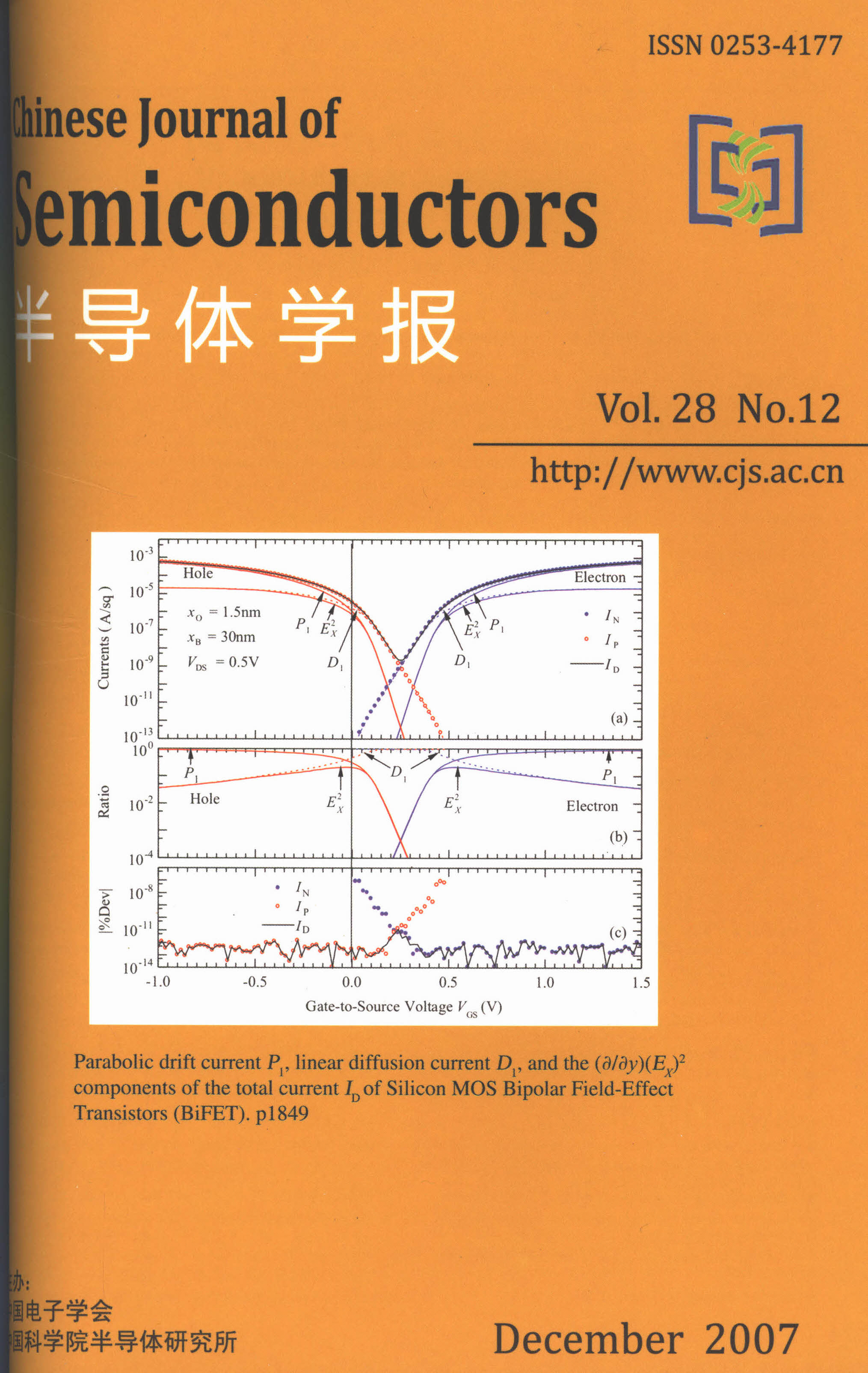
This paper describes the drift-diffusion theory of the bipolar field-effect transistor (BiFET) with two identical and connected metal-oxide-silicon-gates (MOS-gates) on a thin-pure-base.Analytical solution is obtained by partitioning the two-dimensional transistor into two one-dimensional problems coupled by the parametric surface-electric-potential.Total and component output and transfer currents and conductances versus D.C.voltages from the drift-diffusion theory,and their deviations from the electrochemical (quasi-Fermi) potential-gradient theory,are presented over practical ranges of thicknesses of the silicon base and gate oxide. A substantial contribution from the longitudinal gradient of the square of the transverse electric field is shown.
By epitaxial layer structure design and key fabrication process optimization,a lattice-matched InP-based In0.53Ga0.47As-In0.52Al0.48As HEMT with an ultra high maximum oscillation frequency (fmax) of 183GHz was fabricated.Thefmax is the highest value for HEMTs in China.Also,the devices are reported,including the device structure,the fabrication process,and the DC and RF performances.
Lattice-matched In0.53Ga0.47As/In0.52Al0.48A high electron mobility transistors (HEMTs) with a cutoff frequency (fT) as high as 218GHz are reported.This fT is the highest value ever reported for HEMTs in China.These devices also demonstrate excellent DC characteristics:the extrinsic transconductance is 980mS/mm and the maximum current density is 870mA/mm.The material structure and all the device fabrication technology in this work were developed by our group.
A 4~12GHz wideband power amplifier,using a balanced configuration with a strip line Lange coupler,is designed and fabricated.This power amplifier shows a maximum continuous wave output power of 295dBm at 8GHz center frequency with an associated gain of 8.5dB and a gain flatness of +/-0.6dB in the 4~12GHz frequency range.
A high-accuracy,low-dropout (LDO) voltage regulator is presented.Using the slow-rolloff frequency compensation scheme,the LDO effectively overcomes the stability problem,facilitates the use of a ceramic capacitor,and improves the output voltage accuracy,which is critical for powering high-performance analog circuitry.The slow-rolloff compensation scheme is realized by introducing three pole-zero pairs,including the proposed pole-zero pair and sense zero.The post-layout simulation results demonstrate that this LDO has robust system stability,a high open-loop gain,and a high unit-gain frequency,which lead to excellent regulation and transient response performance.The line and load regulation are 27μV/V and 3.78μV/mA,and the overshoots of the output voltage are less than 30mV,while the dropout voltage is 120mV for a 150mA load current.
A small-signal equivalent circuit model and the extraction techniques for photodetector chips are presented.The equivalent lumped circuit,which takes the main factors that limit a photodetector's RF performance into consideration,is first determined based on the device's physical structure.The photodetector's S parameters are then on-wafer measured,and the measured raw data are processed with further calibration.A genetic algorithm is used to fit the measured data,thereby allowing us to calculate each parameter value of the model.Experimental results show that the modeled parameters are well matched to the measurements in a frequency range from 130MHz to 20GHz,and the proposed method is proved feasible.This model can give an exact description of the photodetector chip’s high frequency performance,which enables an effective circuit-level prediction for photodetector and optoelectronic integrated circuits.
The properties of a bound polaron in a parabolic quantum dot with weak electron-LO-phonon coupling under a Coulomb field are studied.The ground state energy of the bound polaron is derived by using a linear combination operator and the perturbation method.The influence of the interaction between phonons with different wave vectors in the recoil process on the ground state energy of the bound polaron is discussed.Numerical calculations are performed,and the results show that the ground state energy increases significantly as the effective confinement length of the quantum dot decreases,considering of the interaction between phonons.Whenl0>1.0,the influence of the interaction between phonons on the ground state energy cannot be ignored.
Pure metal Fe films with thickness of about 100nm were deposited on Si (100) substrates by DC magnetron sputtering.Annealing was subsequently performed in a vacuum furnace in the temperature range of 600~1000℃ for 2h.The samples were characterized by means of Rutherford backscattering (RBS) with 3MeV carbon ions.The RBS data were fitted with SIMNRA 60,and the results show the atomic interdiffusion in Fe/Si systems.The microstructures and crystal structures were characterized by scanning electron microscope and X-ray diffraction.The effects of annealing on atomic interdiffusion,silicide formation,and microstructures in Fe/Si systems were analyzed.
Surface phonon-polaritons in slabs of polar ternary mixed crystals are investigated with the modified random-element-isodisplacement model and the Born-Huang approximation,based on Maxwell’s equations with the usual boundary conditions.The numerical results of the surface phonon-polariton frequencies as functions of the wave-vector and thickness for slabs of ternary mixed crystals AlxGa1-xAs,ZnxCd1-xS,and GaxIn1-xN are obtained and discussed.It is shown that there are four branches of surface phonon-polaritons in slab systems.The "two-mode" and "one-mode" behaviors of surface phonon-polaritons are also shown in their dispersion curves.
A high gain cascade connected preamplifier for optical receivers is developed with 0.5μm GaAs PHEMT technology from the Nanjing Electronic Devices Institute.To begin with,the transimpedance amplifier has a -3dB bandwidth of 10GHz,with a small signal gain of around 9dB.The post-stage distributed amplifier (DA) has a -3dB bandwidth of close to 20GHz,with a small signal gain of around 12dB.As a whole,the cascade preamplifier has a measured small signal gain of 213dB and a transimpedance of 55.3dBΩ in a 50Ω system.With a higher signal-to-noise ratio than that of the TIA and a markedly improved waveform distortion compared with that of the DA,the measured output eye diagram for 10Gb/s NRZ pseudorandom binary sequence is clear and symmetric.
A high characteristic temperature (T0) of 200K from a 1.3μm AlInGaAs/AlInAs single-quantum-well laser diode with the asymmetric waveguide layer structure under CW operation at 20 to 80℃ was obtained,which is the best result reported in the laser diodes (LDs) of the same active materials structure and emitting wavelength.AlInGaAs as an active layer,therefore,is very promising for the fabrication of long-wavelength LDs with excellent high-temperature performance.It is found that the asymmetric waveguide layer structure can decrease optical absorption and improve the high-temperature performance and catastrophic optical damage threshold of LDs.
A new physical current-voltage model for polysilicon thin-film transistors (poly-Si TFTs) is presented.Taking the V-shaped exponential distribution of trap states density into consideration,explicit calculation of surface potential is derived using the Lambert W function,which greatly improves computational efficiency and is critical in circuit simulation.Based on the exponential density of trap states and the calculated surface potential,the drain current characteristics of the subthreshold and the strong inversion region are predicted.A complete and unique drain current expression,including kink effect,is deduced.The model and the experimental data agree well over a wide range of channel lengths and operational regions.
A low-power-consumption 9bit 10MS/s pipeline ADC,used in a CMOS image sensor,is proposed.In the design,the decrease of power consumption is achieved by applying low-power-consumption and large-output-swing amplifiers with gain boost structure,and biasing all the cells with the same voltage bias source,which requires careful layout design and large capacitors.In addition,capacitor array DAC is also applied to reduce power consumption,and low threshold voltage MOS transistors are used to achieve a large signal processing range.The ADC was implemented in a 0.18μm 4M-1P CMOS process,and the experimental results indicate that it consumes only 7mW,which is much less than general pipeline ADCs.The ADC was used in a 300000 pixels CMOS image sensor.
Dual-modulus prescalers (DMP) for RF receivers are studied.An improved D-latch is proposed to increase the speed and the driving capability of the DMP.A novel D-latch architecture integrated with ‘OR’ logic is proposed to decrease the complexity of the circuit.A divided-by-16/17 DMP for application in a digital video broadcasting-terrestrial receiver is realized with a TSMC 0.18μm mixed-signal CMOS process.The programmable & pulse swallow divider in this receiver is designed with a 0.18μm CMOS standard cell library and realized in the same process.The measured results show that the DMP has an output jitter of less than 0.03% and works well with the programmable & pulse swallow divider.
An ultra-low dislocation density of 1.2e5cm-2,95% strain relaxed,compositionally graded SiGe layer formed by dry oxidizing the strained Si0.88Ge0.12 alloy on Si (100) substrates at 1000℃ was prepared.By comparing samples with various oxidation times,the relaxation mechanisms of the strained SiGe layers during the oxidation processes were analyzed.
J-V characteristics of Cu(In1-xGax)Se2 (CIGS) thin film solar cells are measured and analyzed.The diode saturation current density J0,diode quality factor A,series resistance Rs and shunt resistance rsh are deduced using Matlab.The calculated results coincide with the measurement very well.A CIGS cell produced in our laboratories is characterized at different illumination intensities.The calculated characteristic parameters are plotted with the irradiance.The shunt resistance rsh decreases as illumination increases.The increased shunt resistance is most likely one of the reasons for the better performance of CIGS solar cells under week illumination.
InGaAs/AlAs RTD material structure on InP substrate is designed and grown by molecular beam epitaxy.A device with good negative differential resistance characteristics and a higher resistive cutoff frequency is fabricated using mesa isolation,metal lift-off,wet chemical etch,and air bridge technologies.The forward bias peak-to-valley current ratio (PVCR) and reverse bias PVCR are about 17.5 and 28,respectively.The peak current density is 56kA/cm2,and the data fitting resistive cutoff frequency using an RNC circuit model is 82.8GHz.The experiment lays a foundation for the design and fabrication of high-performance RTD and monolithic integration circuits of RTD and other high speed and high frequency three terminal devices.
High quality GaN HEMT materials were grown on Si (111) substrates by MOCVD.The FWHM of the XRD (002) rocking curve of the 1mm-thick GaN epilayer is 573" ,and the (102) is 668" .2μm-thick crack-free GaN HEMT materials were achieved by the interlayer technique.The RT 2DEG mobility is 1350cm2/(V·s) with a sheet resistance of 328Ω/□.The DC and RF characteristics of a GaN microwave power device with a 1mm gate width were probed.The saturated drain current density is around 0.8A/mm,and the peak transconductance is beyond 250mS/mm.Tuning for a maximum output power of 5.1W at 2GHz,a gain of 9.1dB,and a peak power-added efficiency of 35% was obtained.
The reflective spectra of SiO2/Al,ITO/Al,SiO2/Au,and ITO/Au omni-directional reflector (ODR) structure and the distributional Bragg reflector (DBR) are calculated by computer simulation.The DBR is grown by LP-MOCVD,then the glass/SiO2/Au ODR samples are fabricated by PECVD and magnetron sputtering,and finally the reflective spectra of those samples are measured.The experimental results are approximately in agreement with the simulations.The reflectivity of the SiO2/Au ODR is as high as 91% for 630nm normal incidence light.The SiO2/Au reflectivity remains a high value when the incidence light angle changes from 20° to 85°,which is much higher than the reflectivity of DBR.The results from the LED device indicates that light intensity on axis of the LED with ODR structures increases by 115% compared with that of LED without DBR,and increases by 28% compared with that of the LED with DBR.These results show the ODR structure can strongly increase the luminous efficiency of the red LEDs.
AlGaN-based resonant-cavity-enhanced p-i-n photodetectors operating at a wavelength of 320nm were designed.A 40.5-pair AlN/Al0.3Ga0.7N distributed Bragg reflector and the air/GaN interface,serving as the back and front mirror,respectively,form a resonant cavity.In the cavity there is a p-GaN/ i-GaN/ n-Al0.38Ga0.62N structure.The wafer was fully epitaxial on the sapphire substrate and GaN template by metalorganic chemical vapor deposition.The response spectrum exhibits selective enhancement at 313nm,with a responsivity of 14mA/W under zero bias.
Based on the JFET theory,a smart,high-voltage SENSFET that adopts double RESURF is designed.The implant dose,the start point,the length of the lower electric field layer Pwell2,and the implant dose of Nwell are optimized,and thus we obtain a SENSFET with a breakdown voltage of 730V and a linear resistance of 7.2e5Ω·μm.The experimental results show that the breakdown voltage is 700V and the linear resistance is 10kΩ when the width of the SENSFET is 75μm.The experimental results agree with the numerical results.The SENSFET is used as the detector and self-supply of a smart power integrated circuit.
This paper presents the design of a variable gain amplifier with wideband and linear-in-dB gain control based on a TSMC 0.18μm RF CMOS process.The circuit of the amplifier consists of two gain stages.The first stage is a cascode amplifier with voltage-shunt negative feedback for good input impedance matching and noise figure performance.The second stage adopts the signal-summing structure to achieve gain control.A new exponential function circuit is added to solve the problem that the gain of amplifier and the control voltage is not a linear relationship,which caused by the non-exponential relationship between drain-source current and gate-source voltage,making the gain become linear in dB along with the control voltage.Measurement results show that the amplifier consumes 9mA at 1.8V.The 3dB bandwidth is 430~2330MHz.The circuit has a controllable gain range of -3.3~9.5dB.The noise figure is 6.2dB at maximum gain,and the input P1dB at minimum gain is -9dBm.
A novel parasitic auto-correction precision silicon temperature sensor in a 0.5μm CMOS process is presented.Simulation shows that its accuracy is within ±03℃ in the full military temperature range from -55 to 125℃ with just one point calibration at 300K.This result is achieved by canceling the base resistor of the CMOS substrate pnp transistors with two structures:three bias temperature sensors and a novel switch-capacitor Sigma-Delta ADC analog front end.The bias current and the emit area of pnp transistors are carefully chosen to avoid serious nonlinearity and a novel analog front end is controlled by four non-overlapping clocks to ease digital processing after ADC.
A new multi-scale model based on the energy conversation law is presented to calculate the static bending of a nanometer double clamped silicon beam.This model accounts for the discrete nature in the thickness of the beam and it can be used in the range of the nanometer scale to the micrometer scale.It is shown that the surface relaxation has a significant effect on the deflection behavior when the beam is scaled down to nanosize.Compared with the continuum theory in the micrometer scale,the multi-scale model agrees with the macro-model in the micrometer scale.
The unique negative differential resistance characteristics lead the RT (resonant tunnel) devices to multiple-valued applications.In this paper,an RT switching circuit model is proposed,ternary NAND and NOR circuits are designed based on the switching sequence theory using RT devices,and they have correct logic certified by the SPICE simulation using MOS net model.This method can be used in other multiple-valued circuits design.
A charge-pump circuit that can be used in PLL is achieved through a TSMC 0.18μm CMOS process.Conventional CMOS charge pump circuits have large current mismatch.The current mismatch can generate a phase offset,which increases spurs in PLL outputs and reduces the locking range.An operational amplifier, self-biasing cascode current mirror, and supply-independent reference current source are used to make the charge and discharge current match.Measurement results show that the charge pump current is 0.475mA and the current mismatch is less than 10mA in the output voltage range of 0.3~1.6V,with power consumption of 6.8mW at 1.8V.
A fully differential charge pump for a frequency synthesizer is proposed.The pump eliminates the effect of channel-length modulation and makes the charging and discharging currents match perfectly in a wide output range to minimize the ripple of the control voltage.A common-mode feedback circuit with rail-to-rail input range is employed to ensure a large unrestricted swing of the charge pump.The proposed fully differential charge pump is designed and fabricated in a 1.8V SMIC 0.18μm CMOS mixed-signal process;the chip area is about 450μm×280μm;and the power dissipation is 1mW.A reference spur level of -73dBc is achieved in the worst case,satisfying the performance of the frequency synthesizer.
Aimed at improving test accuracy of analog VLSI circuits,an approach based on digital signal processing (DSP) is presented.Sub-band filtering to test response signals is achieved with a filter bank implemented by Cosine modulation.Energy computing and correlation analysis follow sequences acquired from sub-band filtering.Consequently,digital signature extraction to analog response signal is executed.Experiments to 19 faults in an international Benchmark circuit show that energy computation of a sub-band sequence is applicable for diagnosing hard faults,and correlation analysis has high effectiveness for both hard faults and soft faults.It is also shown that the fault resolution of the approach presented in this paper is much higher than the one reported in Ref.7].
Large area transmission gratings (TG) for soft X-ray diffraction,with an area of 10mm×0.5mm,a period of 500nm,a line-space ratio of 1∶1,and a gold thickness of 430nm,are successfully fabricated by combining electron beam lithography (EBL),X-ray lithography (XRL),and electroplating.In the processes,the mask of TG with well-defined three dimensional relief structures is originally patterned by EBL and then by electroplating.Next,the processes of XRL and electroplating allow us to efficiently and cost-effectively fabricate many copies of TG with the following two major advantages:high resolution and a vertical cross section.Moreover,the measurement of its efficiency has shown its perfect performance with respect to diffraction of EUV light.
According to a Fresnel diffraction model,and considering the reflection and refraction at the glycerol/SU-8 interface,this paper simulates the aerial image when glycerol is applied between the photomask and resist.Compared to the experimental results,the model can describe the lithography process competently and be applied in design.
A novel mathematical model based on the force balance of wafer/particle/pad is developed for chemical mechanical polishing (CMP).The main feature of the model is the incorporation of the particle adhesion force and the large deformation of the particle and pad.The model shows that the adhesion force can significantly influence the load force of particles and the indentation depth of particles into Cu and SiO2 wafer surfaces.Furthermore,the model also predicts that the indentation depth of the particle into the wafer surface considering the adhesion force is two or four times than that of without an adhesion force.However,the magnitude of the indentation depth is on the order of molecular scale.The results and analysis reveal some insights into the molecular scale removal mechanism on the performance of the CMP.