The hydrogen plasma degradation of transparent conduction oxides (TCO) is studied for hydrogenated microcrystalline Si(μc-Si:H)prepared by plasma enhanced chemical vapor deposition (PECVD).TCO films such as SnO2 and SnO2/ZnO bi-layer films were exposed to atomic H at various substrate temperatures and for various treatment times.A decrease in the transmittance due to reduction by atomic H was scarcely observed for SnO2/ZnO bi-layer,while a decrease for SnO2 was found to depend strongly on the substrate temperature.The resistivity of SnO2 films decreases significantly when substrate temperature exceeds 150℃ in H-plasma.However,H-plasma treatment has little impact on the resistivity of SnO2/ZnO bi-layer film.The reason for the decrease in the transmittance is the appearance of metallic Sn on the surface,and under this condition no μc-Si:H film is deposited.SnO2/ZnO bi-layer is very effective for the suppression of the reduction of TCO during μc-Si:H deposition.The performance of microcrystalline silicon solar cells fabricated on ZnO/SnO2/glass is also investigated.
AFM scanning images of the surface of a PTCDA/p-Si specimen used in an organic/inorganic photodetector show that PTCDA grows in island shapes that are poorly distributed,with each island shaped like a round hillock.The images also show that there exist enormous defects in the PTCDA layer due to pedestal sites and other defects that appear when Si atoms shift transversely,and that the bonding condition is satisfied by the action of atom suspension bonding at the surface of the Si substrate.We infer the growth mode of PTCDA deposited onto p-Si substrates as follows.First,PTCDA molecules assemble at the defects to form three-dimensional island-like PTCDA crystal nuclei,and then by the action of delocalized big π bonding,two adjacent layers of PTCDA molecules overlap to some extent and finally island-like structures form.The PTCDA molecules and Si substrate combine by a process of the combination of benzene rings with Si atoms at the defects and of acid anhydride radicals with Si atoms at the perfect fraction of the surface.In the course of combination,although the structure of the benzene rings does not change,the chemical reaction of acid anhydride radicals and Si occurs to break off the CO bond in the acid anhydride,and then C-Si-O and silicon oxide might be produced.
A polarization-maintaining (PM) fiber Mach-Zehnder (MZ) interferometer has been established to measure the EO effect of very thin film materials with optical anisotropy.Unlike a common MZ interferometer,all the components are connected via polarization-maintaining fibers.At the same time,a polarized DFB laser with a maximum power output of 10mW is adopted as the light source to induce a large extinction ratio.Here,we take it to determine the electro-optical coefficients of a very thin superlattice structure with GaAs,KTP,and GaN as comparative samples.The measured EO coefficients show good comparability with the others.
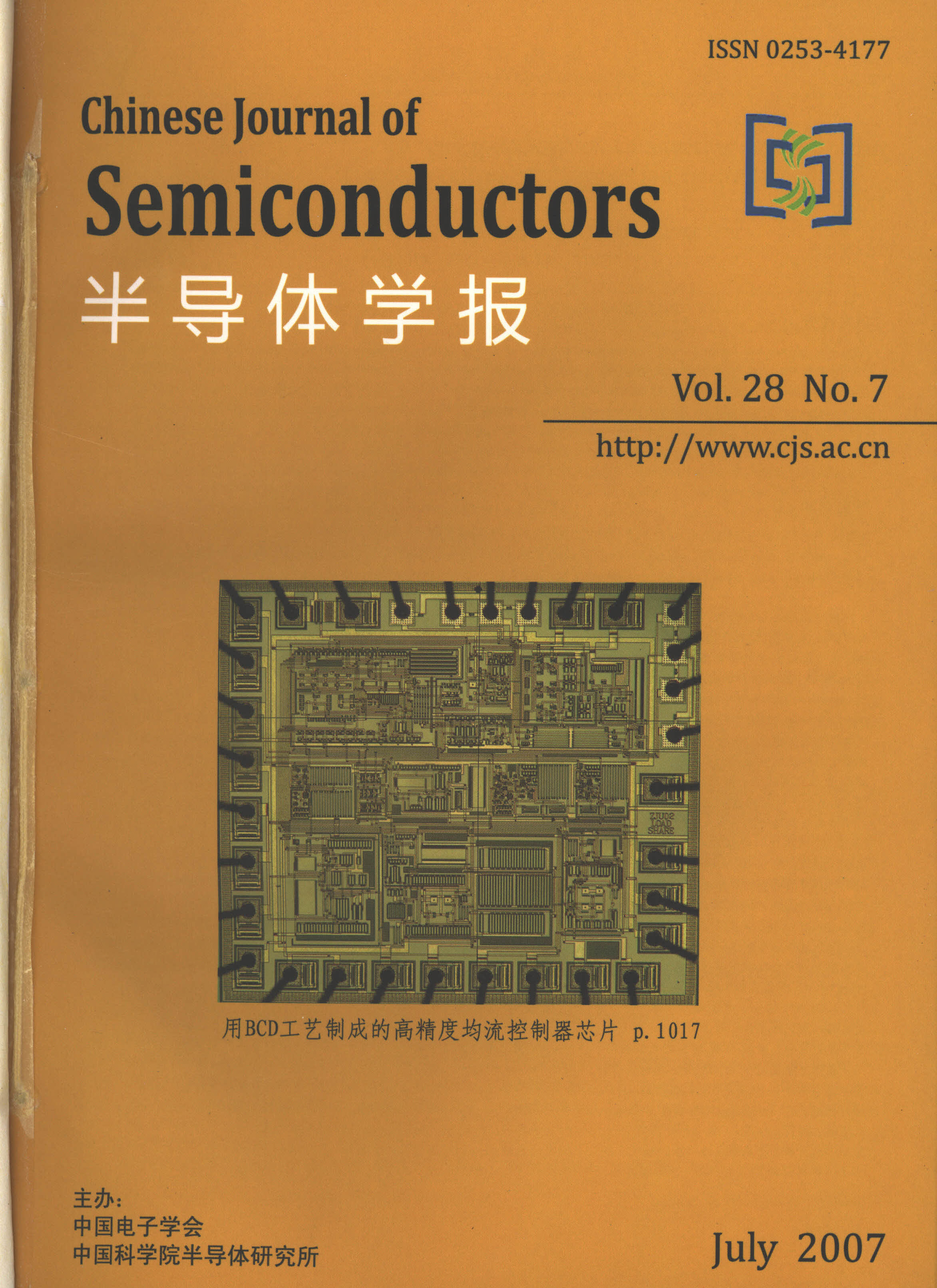
To keep even current distribution among DC/DC converters in a paralleled power system,an automatic master-slave control (AMSC) current sharing scheme is presented,which was implemented by a current share control IC.A current feedback loop for output voltage adjustment is proposed for low signal distortion.Moreover,a special startup control logic is designed to improve startup timing and to speed up the initial current sharing.It was completed in 1.5μm bipolar-CMOS-DMOS (BCD) technology with an area of 3.6mm2.Using it,a paralleled power system of two DC/DC converters capable of outputting 12V/3A was built.Experimental results show that the current sharing error at full load is kept within 1%.
A new comprehensive empirical large signal model for 4H-SiC MESFETs is proposed.An enhanced drain current model,along with an improved charge conservation capacitance model,is presented by the improvement of the channel length modulation and the hyperbolic tangent function coefficient based on the Materka model.The Levenberg-Marquardt method is used to optimize the parameter extraction.A comparison of simulation results with experimental data is made,and good agreements of I-V curves,Pout(output power),PAE (power added efficiency),and gain at the bias of VDS=20V,IDS=80mA as well as the operational frequency of 1.8GHz are obtained.
A design for a Li-ion battery charger IC that can operate in a constant current-constant voltage (CC-CV) charge mode is proposed.In the CC-CV charge mode,the charger IC provides a constant charging current at the beginning,and then the charging current begins to decrease before the battery voltage reaches its final value.After the battery voltage reaches its final value and remains constant,the charging current is further reduced.This approach prevents charging the battery with full current near its saturated voltage,which can cause heating.The novel design of the core of the charger IC realizes the proposed CC-CV charge mode.The chip was implemented in a CSMC 0.6μm CMOS mixed signal process.The experimental results verify the realization of the proposed CC-CV charge mode.The voltage of the battery after charging is 4.1833V.
A direct conversion CMOS DVB-S front-end employs a T-configuration variable attenuator,a single-to-differential low noise amplifier,and a low noise mixer.By innovative use of the attenuator,the linearity handling ability of the system is dramatically improved.The system is designed and fabricated in SMIC 0.18μm RF CMOS technology.The measurement data show that the front-end provides a total of more than 30dB dynamic range and a noise figure of 5dB in the wide frequency signal band.The prototype front-end consumes only 10mA and achieves an IIP3 of +20dBm.
Based on Chin's theory,which describes the concentration and compensation ratio dependencies of the low-field mobility in gallium nitride in wide concentration ranges (1e16~1e20cm-3) at room temperature,an analytic model for the compensation ratio of unintentionally doped GaN at room temperature has been obtained.Another model for Si-doped GaN has also been obtained by use of theoretical calculations and computational methods.A comparison of these models with the fitting value from experimental results shows that the new analytic models have a good agreement in the electron concentration range of 3e16~1e18cm-3.
A three-dimensional model of a silicon nano-plate with native oxide is proposed.The energy approach is used to obtain the Young’s moduli of the silicon nano-plate with and without the oxide layer.It is shown that the Young’s modulus of the nano-plate with surface oxide increases with the decrease of the nano-plate thickness,while that without surface oxide exhibits the opposite behavior.The reason is that the native oxide layer dominates the plate as it scales down to several nanometers.As the plate increases to 300nm,the Young’s moduli approach 123GPa.The Young’s modulus increases as the oxide thickness increases.When the thickness is 50nm,the Young’s moduli are in the range of 120 to 200GPa.
DMS GaMnN film with a certain concentration of Mn and good crystal qualities was successfully grown on sapphire substrate (α-Al2O3) by ECR-PEMOCVD.The RHEED graphs present a clear spot-like lattice and a surface that is not very smooth,indicating that the GaMnN film is single crystalline and its growth mode was three-dimensional island.XRD analysis shows that the film has a hexagonal structure with c-xis orientation and very good crystallinity.The AFM test result shows that the GaMnN films are composed of many submicron grains with the same orientation.Superconducting quantum interference device (SQUID) measurement shows apparent ferromagnetism at room temperature,and the Curie temperature of the film is about 400K.
Diluted magnetic semiconductor Mn0.1Ti0.9O2-δ(MTO) thin film was grown successfully on SrTiO3(STO) substrate by oxygen plasma assisted molecular beam epitaxy (OPA-MBE).The crystalline structure,chemistry composition,optical absorption,and electrical conductivity properties of the thin film were characterized by X-ray diffraction (XRD),X-ray photoelectron spectrometry (XPS),ultraviolet and visible spectrophotometry (UV-Vis),and resistivity measuring instruments with a four-probe array.The MTO thin film has anatase and rutile crystal structures,and the absorption edge is shifted to the lower-energy.The electrical conductivity of the MTO thin film is evidently improved,and the resistivity is only 37.5Ω·m at room temperature.
8-hydroxylquinline cadmium(Cdq2)thin films were prepared on glass substrate using vacuum coating technology at different substrate temperatures.The surface and structure were investigated using atomic force microscopy(AFM)and X-ray diffusion(XRD),respectively.The results show that Cdq2 thin film is polycrystalline in structure,and higher substrate temperature results in better morphology,larger grain size,and better structure order.The spectroscopic ellipsometry results show that the refractive index and extinction index decrease with increasing wavelength,and the value of the refractive index and extinction coefficient increase as the substrate temperature increases.
Hg3-3xIn2xTe3(MIT)(x=0.5) single crystals were successfully grown using the vertical Bridgman method (VB) and were investigated by XRD,RO-XRD,and Hall measurements.The results show that the as-grown crystal is high quality single-phase crystal.The wafer surface is (311) face,and the crystal face is located at θ=23.86°.The spatial deviation angle of the (311) face is φ=2.9°,and the degree of orientation scatter is FWHM=0.3°.The crystal is an n-type semiconductor.The resistivity,carrier concentration,and carrier mobility are 4.79e2Ω·cm,2.83e13cm-3,and 4.6e2cm2/(V·s),respectively.The Fermi level lies near the midgap and is about 8meV higher.The calculated values of the carrier concentration are in agreement with the experimental ones.
The structural,optical,and electrical properties of ZnO thin films grown by metal organic chemical vapor deposition at different B2H6 flow rates were investigated.XRD spectra and SEM images indicate that all the ZnO films have the preferential orientation of (110) peak,showing textured surfaces.When the B2H6 flow rate was set at 10sccm,a low sheet resistance (12Ω/□) and high average transparency (>80%) in the range of visible light and infrared and 30.5cm2/(V·s) mobility were obtained for 1000nm thick ZnO film deposited on 6cm×6cm glass substrate at a low temperature of 423K.PL spectra indicate that boron-doping improves the crystal quality,which explains why the ZnO:B films show a better electrical stability than the un-doped samples.Low-pressure annealing in H2 atmosphere at 473K of ZnO films effectively enhances the electron mobility.When applied in a-Si thin film solar cells as front electrodes,ZnO films present equivalent performance to Asahi-U type SnO2 films
HgCdTe epilayer grown on(211)Si/CdTe compound substrate was first obtained by a novel liquid-phase epitaxy technique.The etch pit density of the layer is about (5~8)e5cm-2,which is lower than that grown by MBE.The FWHM of the X-ray rocking curve of the epilayer can be better than 70" .The control level of composition and thickness of the epilayer is the same as that of the HgCdTe routine LPE technique on (111) CdZnTe substrate.But the density of surface defects on (211) HgCdTe layer is higher than that of epilayer grown on (111) CdZnTe substrate at present.The result indicates that (211) Si-based HgCdTe LPE can play an important role in growing low etch pit density Si-based HgCdTe materials used for the fabrication of longwave infrared focal plane arrays.
SiOx nanowires were successfully fabricated by a hydrothermal method using SiO powder as raw material.SEM and TEM photos show that the diameter and the length of these nanowires are about 100~200nm and tens of microns,respectively.EDS was introduced to quantitatively analyze the components and show that SiOx nanowires are only composed of Si and O.The PL spectrum shows that the nanowires have two fluorescent excitations at 426 and 446nm.The best preparation condition has been obtained by a series of contrastive experiments with different conditions.Meanwhile,a mechanism is given in this letter for the synthesis of SiOx nanowires by the hydrothermal method.
GaSb thick layers were grown by molecular beam epitaxy on GaAs(100)substrates.High quality InAs/GaSb superlattices(SLs)with different InAs thicknesses were grown on GaSb buffer layers on GaAs substrates.The peak wavelengths of photoluminescence spectra at 10K are between 2~2.6μm.High-resolution transmission electron microscopy shows that the SLs have clear interface and integrated periods.
Bonding of GaAs/GaN was successfully achieved at 600℃ in N2 atmosphere for 1h,with two different chemical pretreatments of hydrophilic and hydrophobic processes.Both methods can achieve high bonding strength and large bonding area.Based on the mechanics of the two different pretreatments,the transmittance of the bonding interface with different pretreatments was studied.Results of the transmission spectrum indicate that the hydrophobic process can yield a higher transmittance of 94.7% at 630nm.Devices were fabricated to execute the EL spectrum measurement,the results of which are consistent with the transmission spectrum.
The plasma-induced damage for p-GaN by inductively coupled plasma(ICP) etching with Cl2/N2 gas chemistry was studied.Effects of ICP power,RF power,chamber pressure,and Cl2 percentage on the physical and electrical characteristics of p-GaN were investigated.The results show that the surface roughness is relatively independent of these etching conditions and shows fairly smooth morphology (RMS<1.2nm);the surface morphology has no direct effect on the electrical characteristics of p-GaN,and the deterioration of ohmic contact to the etched p-GaN is due to a decrease in hole concentration in the near-surface region through the creation of shallow donor states rather than surface roughening.
A 19.2mm gate-width GaAs power HFET has been fabricated with improvements in the technology of device structure and passivation.The internally-matched device with two chips yields an output power greater than 42dBm(158W) with more than 7dB power gain,more than 35% PAE,and more than 90% co-efficiency across the band of 13.7~14.5GHz with Vds=9V and Pin=35dBm.At 14.3GHz,an output power of 42.54dBm (17.9W) and power gain of 7.54dB were achieved.
Based on the conception of RTD/HEMT series connection resonant tunneling transistors,an RTD/HEMT monolithic integration material structure was designed and grown by molecular beam epitaxy.RTT was fabricated using wet chemical etching,metal lift-off,mass isolation,and air bridge technologies.The device has a distinct gate-controlled negative differential resistance.The maximal peak-to-valley current ratio (PVCR) of the forward direction connection RTT is about 2.2 and the maximal PVCR of the backward direction connection RTT is about 4.6.This experiment lays a foundation for the optimization of RTT and RTD/HEMT monolithic integration circuit development.
Using the junction temperature distribution as determined from infrared imaging,the thermal spectrum curve is obtained by thermal spectrum analysis for use in creating a "sub-transistors in parallel connection" model.Based on the model,from theoretical calculation and experiment,the validity of the excessive thermotaxis effect of low current is verified.For current passing through a pn junction in a non-uniform temperature distribution,there is much more thermotaxis at low current than at high current,i.e.,with decreasing measured current,the ratio of the current density at high-temperature to that at low-temperature increases,and the effective area decreases.Based on these characteristics,the electro-thermal instability and the degree of uniformity of the junction temperature distribution can be studied.This has great significance for the reliability analysis of semiconductor devices.
A 1.55μm InP-InGaAsP quantum-well laser was fabricated on Si substrate by low-temperature wafer bonding,which lases at room temperature with electrical pumping.The InP epitaxy was designed and grown by MOCVD,then bonded to Si wafer.Finally,the laser with ridge-waveguide and edge-emission was fabricated.This laser runs continuous-wave with a threshold current of 48mA (current density of 1.65kA/cm2),differential resistance of 5.8W at the threshold current,and a maximum output power of 15mW at 220mA.
InGaN/GaN multiple quantum well (MQW) light emitting diode (LED) wafers with two emission peaks were grown by MOCVD.Transmission electron microscopy (TEM),electroluminescence (EL),and cathodoluminescence (CL) measurements were performed to study the recombination mechanism of the InGaN QWs.It was found that there are different widths of quantum wells in TEM images.Green and blue emissions were separately observed in the EL spectra,which are located at 2.45 and 2.81eV,respectively.The wavelengths for both the blue and green emission do not shift until the injection level reaches 2e4mA/cm2.In monochromatic CL images,the green emission comes from randomly distributed dots and floccules that occupy almost the whole surface.The blue emission comes from the floccules only.It can be concluded that the blue emission is attributed to the irradiative recombination in the QWs,and the green emission is attributed to that in wider QWs and In-rich QDs.
An improved thermal model for a vertical cavity surface-emitting laser is proposed.The model is based on Tucker’s model of the laser diode.The voltage-current (V-I) characteristic of the laser is given by introducing the thermal effect to the parasitic resistance and to the reverse saturation current.The light output power-current (L-I) characteristic is given by adding a thermal related leakage current to the model.The model proposed in this paper is more practical than thermal models proposed in the reference,and model parameters can be easily extracted with methods that have been presented by other authors. The model is implemented into SPICE-like simulators including HSPICE,and the simulated and measured V-I characteristics and L-I characteristics exhibit a good agreement over a wide range of ambient temperature.
Photosensitive sol-gel SiO2 materials were synthesized by the organic-inorganic hybrid method,and were spun on silicon substrate.The effects of UV-light exposure time and the postbake temperature and time on the refractive index and depth of the films were investigated.1×2 and 1×4 MMI splitters were fabricated by means of UV-light imprinting technology,and good mode profiles were measured.
In order to reduce the reset current of C-RAM devices,a W sub-micron tube heating electrode with external diameter of 260nm was fabricated in standard 0.18μm CMOS,and its electrical performance was characterized.A typical C-RAM device was manufactured using a W sub-micron tube heating electrode,and the causes of invalidation were analyzed through fatigue behaviour testing.The results indicate that a W sub-micron tube heating electrode with favourable electrical stability and fatigue behaviour,as well as thermal stability,provides an efficient path for reducing the reset current of a C-RAM device.
A radiation-hardened 128kbit asynchronous SRAM fabricated in partial depletion silicon on insulator substrate is presented.Special characteristics of SOI devices are used in the design process.After careful circuit design,hierarchical layout design,and simulation of critical path,the SRAM chip was fabricated in the first turn-out.Besides the radiation-hardened characteristics of SOI material,fully-body-tied 6T memory cell and H-type gate MOSFETs techniques are also implemented in this PDSOI SRAM.These advanced techniques reduce the power consumption and raise the radiation-hardened level of this SRAM.The final testing shows that the 128k bit SOI SRAM has a typical operating current of 20mA at 10MHz,total dose tolerance of 500krad(Si),and dose rate survivability of 2.45e11rad (Si)/s.The implementation of radiation-hardened 128k SOI SRAM will accelerate the development of PD SOI CMOS processes,and will surely contribute more to the radiation design of VLSI circuits in the future.
A novel structure of an inline type microwave power sensor is presented based on MEMS technology.The theory,design,fabrication,and measurements are given.The microwave power coupled from the CPW line is measured by the MEMS membrane.The fabrication process of this power sensor is fully compatible with a GaAs MMIC process.In this method the signal is available during power detection.The results show that the sensor has a reflection of less than -15dB and an insertion loss of less than 2.0dB up to 12GHz.The sensitivity of this power sensor is 10.4μV/mW at 10GHz.
A design of a low-dropout (LDO) voltage regulator with an output current of 800mA is proposed.By introducing a zero-pole tracking circuit with a MOS resistor working in the linear region,the frequency response is independent of the load current.Moreover,with ameliorated miller compensation,a 60° phase margin is guaranteed.Based on the analysis of slewing behavior versus circuit parameters,the load regulation property is improved with a slew rate enhancement circuit which can supply a large current to speed up the slew rate.The precision of the output voltage is maintained within ±60mV under varying load conditions from 800 to 10mA,and the settling time is about 500μs.The chip is implemented in CSMC 0.6μm mixed-signal technology.The designed circuit is validated by the results of the chip test.
A novel ESD protection design method is proposed instead of the traditional experience-based trial-and-error electrostatic discharge (ESD) design approach.The new method resolves the costly and time-consuming problems of high-performance ESD protection development in sub/deep-sub micron CMOS technology.The method is conducted and verified in a 0.5μm CMOS process to accomplish I/O cell design of a CMOS ASIC library,whose human-body-model ESD level can be greater than 5kV.
A novel method is used to evaluate the quality of a TFT array for an active matrix OLED,which can measure the characteristics of TFTs in a 2-T pixel circuit and detect the defects.The proposed testing method is carried out simultaneously with the fabrication processes.Without changing the fabrication processes,only one mask is added to judge the working states of the switch transistor and driving transistor in the pixel circuit.It is a current testing method,which has several advantages including fast response time,high precision,and no damage to the display.