Issue Browser
Volume 28, Issue 8, Aug 2007
Column
LETTERS
Storage Characteristics of Nano-Crystal Si Devices Using Different Measurements for MOS Capacitors
Li Wei, Zhang Zhigang, Liang Renrong, He Yang, Wang Liudi, Zhu Jun
Chin. J. Semicond.  2007, 28(8): 1169-1172
Abstract PDF

The storage characteristics of nano-crystal Si (NC-Si) devices,especially for MOS capacitors,are studied by cross sectional transmission electron microscopy (TEM) and capacitance-voltage (C-V) measurement under different conditions,including programming and erasing at different temperatures and gate voltages,as well as using +/-bias-temperature (BT) measurements.Physical mechanisms such as carrier trapping,interface state filling,and temperature related deterioration are revealed.The experimental results demonstrate that the degradation of the program window and threshold voltage (VT) shift at high temperature,large voltage sweep range,and bias applied to sweep voltage is strongly related to the type of majority carriers.

The storage characteristics of nano-crystal Si (NC-Si) devices,especially for MOS capacitors,are studied by cross sectional transmission electron microscopy (TEM) and capacitance-voltage (C-V) measurement under different conditions,including programming and erasing at different temperatures and gate voltages,as well as using +/-bias-temperature (BT) measurements.Physical mechanisms such as carrier trapping,interface state filling,and temperature related deterioration are revealed.The experimental results demonstrate that the degradation of the program window and threshold voltage (VT) shift at high temperature,large voltage sweep range,and bias applied to sweep voltage is strongly related to the type of majority carriers.
Influence of Substrate Temperature and Nitrogen Gas on Zinc Nitride Thin Films Prepared by RF Reactive Sputtering
Zhang Jun, Xie Erqing, Fu Yujun, Li Hui, Shao Lexi
Chin. J. Semicond.  2007, 28(8): 1173-1178
Abstract PDF

Zinc nitride (Zn3N2) thin films were prepared by radio frequency (RF) magnetron sputtering on quartz glass at different substrate temperatures.The structure and composition were characterized by X-ray diffraction and Raman-scattering measurements,respectively.The polycrystalline phase Zn3N2 films appeared when the ratio of the N2 partial pressure to the total pressure reached 1/2.The effects of the substrate temperature on the electrical and optical properties of the Zn3N2 films were investigated by Hall measurements and optical transmission spectra.The electrical and optical properties of the films were highly dependent on the substrate temperature.With the substrate temperature increasing from 100 to 300℃,the resistivity of the Zn3N2 films decreased from 0.49 to 0.023Ω·cm,the carrier concentration increased from 2.7e16 to 8.2e19cm-3,and the electron mobility decreased from 115 to 32cm2/(V·s).The deposited Zn3N2 films were considered to be n-type semiconductors with a direct optical band gap,which was around 1.23eV when the substrate temperature was 200℃.

Zinc nitride (Zn3N2) thin films were prepared by radio frequency (RF) magnetron sputtering on quartz glass at different substrate temperatures.The structure and composition were characterized by X-ray diffraction and Raman-scattering measurements,respectively.The polycrystalline phase Zn3N2 films appeared when the ratio of the N2 partial pressure to the total pressure reached 1/2.The effects of the substrate temperature on the electrical and optical properties of the Zn3N2 films were investigated by Hall measurements and optical transmission spectra.The electrical and optical properties of the films were highly dependent on the substrate temperature.With the substrate temperature increasing from 100 to 300℃,the resistivity of the Zn3N2 films decreased from 0.49 to 0.023Ω·cm,the carrier concentration increased from 2.7e16 to 8.2e19cm-3,and the electron mobility decreased from 115 to 32cm2/(V·s).The deposited Zn3N2 films were considered to be n-type semiconductors with a direct optical band gap,which was around 1.23eV when the substrate temperature was 200℃.
Threshold Voltage Model of a Double-Gate MOSFET with Schottky Source and Drain
Xu Bojuan, Du Gang, Xia Zhiliang, Zeng Lang, Han Ruqi, Liu Xiaoyan
Chin. J. Semicond.  2007, 28(8): 1179-1183
Abstract PDF

A quasi two-dimensional (2D) analytical model of a double-gate (DG) MOSFET with Schottky source/drain is developed based on the Poisson equation.The 2D potential distribution in the channel is calculated.An expression for threshold voltage for a short-channel DG MOSFET with Schottky S/D is also presented by defining the turn-on condition.The results of the model are verified by the numerical simulator DESSIS-ISE.

A quasi two-dimensional (2D) analytical model of a double-gate (DG) MOSFET with Schottky source/drain is developed based on the Poisson equation.The 2D potential distribution in the channel is calculated.An expression for threshold voltage for a short-channel DG MOSFET with Schottky S/D is also presented by defining the turn-on condition.The results of the model are verified by the numerical simulator DESSIS-ISE.
Total Dose Radiation Hardened PDSOI CMOS 64k SRAMs
Guo Tianlei, Zhao Fazhan, Liu Gang, Li Duoli, Li Jing, Zhao Lixin, Zhou Xiaoyin, Hai Chaohe, Han Zhengsheng
Chin. J. Semicond.  2007, 28(8): 1184-1186
Abstract PDF

The first domestic 1e6rad(Si) total dose hardened 1.2μm partially depleted silicon-on-insulator (PDSOI) 64k SRAM fabricated in SIMOX is demonstrated.The address access time is independent of temperature from -55 to 125℃ and independent of radiation up to 1e6rad(Si) for the supply voltage VDD.The standby current is 0.65μA before the total dose of radiation and is only 0.80mA after radiation exposure,which is much better than the specified 10mA.The operating power supply current is 33.0mA before and only 38.1mA afterward,which is much better than the specified 100mA.

The first domestic 1e6rad(Si) total dose hardened 1.2μm partially depleted silicon-on-insulator (PDSOI) 64k SRAM fabricated in SIMOX is demonstrated.The address access time is independent of temperature from -55 to 125℃ and independent of radiation up to 1e6rad(Si) for the supply voltage VDD.The standby current is 0.65μA before the total dose of radiation and is only 0.80mA after radiation exposure,which is much better than the specified 10mA.The operating power supply current is 33.0mA before and only 38.1mA afterward,which is much better than the specified 100mA.
PAPERS
Influence of Coulomb Potential on the Properties of a Polaron in a Quantum Dot
Li Weiping, Xiao Jinglin
Chin. J. Semicond.  2007, 28(8): 1187-1191
Abstract PDF

The ground-state energy and the average number of virtual phonons around the electron of a hydrogenic impurity confined in a parabolic quantum dot are calculated using the squeezed-state variational approach,which is based on two successive canonical transformations and uses a displaced-oscillator type unitary transformation to deal with the bilinear terms,which are usually neglected.Numerical calculations are carried out in order to study the relation between the ground-state energy and the average number of virtual phonons around the electron of a bound polaron in a parabolic quantum dot with the Coulomb binding parameter.The electron-phonon coupling constant and the confinement length are derived.

The ground-state energy and the average number of virtual phonons around the electron of a hydrogenic impurity confined in a parabolic quantum dot are calculated using the squeezed-state variational approach,which is based on two successive canonical transformations and uses a displaced-oscillator type unitary transformation to deal with the bilinear terms,which are usually neglected.Numerical calculations are carried out in order to study the relation between the ground-state energy and the average number of virtual phonons around the electron of a bound polaron in a parabolic quantum dot with the Coulomb binding parameter.The electron-phonon coupling constant and the confinement length are derived.
Improvements on High Current Performance of StaticInduction Transistor
Wang Yongshun, Wu Rong, Liu Chunjuan, Li Siyuan
Chin. J. Semicond.  2007, 28(8): 1192-1197
Abstract PDF

Methods for improving the high current performance of static induction transistor (SIT) are presented.Many important factors,such as "trans-conductance per unit channel width" θ, "gate efficiency" η, "sensitivity factor" D,and "intrinsic static gain" μ0,that may be used to describe different aspects of the electrical performance of an SIT are first defined.The dependences of electrical parameters on the structure and technological process of an SIT are revealed for the first time.The packaging technologies are so important for the improvement of high power performance of SITs that they must be paid attention.Testing techniques and circuits for measuring frequency and power parameters of SITs are designed and constructed.The influence of packaging processes in technological practice on the electrical performance of SITs is also discussed in depth.

Methods for improving the high current performance of static induction transistor (SIT) are presented.Many important factors,such as "trans-conductance per unit channel width" θ, "gate efficiency" η, "sensitivity factor" D,and "intrinsic static gain" μ0,that may be used to describe different aspects of the electrical performance of an SIT are first defined.The dependences of electrical parameters on the structure and technological process of an SIT are revealed for the first time.The packaging technologies are so important for the improvement of high power performance of SITs that they must be paid attention.Testing techniques and circuits for measuring frequency and power parameters of SITs are designed and constructed.The influence of packaging processes in technological practice on the electrical performance of SITs is also discussed in depth.
Design and Implementation of an Optoelectronic Integrated Receiver in Standard CMOS Process
Yu Changliang, Mao Luhong, Song Ruiliang, Zhu Haobo, Wang Rui, Wang Qian
Chin. J. Semicond.  2007, 28(8): 1198-1203
Abstract PDF

A wideband monolithic optoelectronic integrated receiver with a high-speed photo-detector,completely compatible with standard CMOS processes,is designed and implemented in 0.6μm standard CMOS technology.The experimental results demonstrate that its performance approaches applicable requirements,where the photo-detector achieves a -3dB frequency of 1.11GHz,and the receiver achieves a 3dB bandwidth of 733MHz and a sensitivity of -9dBm for λ=850nm at BER=1e-12.

A wideband monolithic optoelectronic integrated receiver with a high-speed photo-detector,completely compatible with standard CMOS processes,is designed and implemented in 0.6μm standard CMOS technology.The experimental results demonstrate that its performance approaches applicable requirements,where the photo-detector achieves a -3dB frequency of 1.11GHz,and the receiver achieves a 3dB bandwidth of 733MHz and a sensitivity of -9dBm for λ=850nm at BER=1e-12.
A 16bit 96kHz Chopper-Stabilized Sigma-Delta ADC
Cao Ying, Ren Tenglong, Hong Zhiliang
Chin. J. Semicond.  2007, 28(8): 1204-1210
Abstract PDF

A 16bit sigma-delta audio analog-to-digital converter is developed.It consists of an analog modulator and a digital decimator.A standard 2-order single-loop architecture is employed in the modulator.Chopper stabilization is applied to the first integrator to eliminate the 1/fnoise.A low-power,area-efficient decimator is used,which includes a poly-phase comb-filter and a wave-digital-filter.The converter achieves a 92dB dynamic range over the 96kHz audio band.This single chip occupies 2.68mm2 in a 0.18μm six-metal CMOS process and dissipates only 15.5mW power.

A 16bit sigma-delta audio analog-to-digital converter is developed.It consists of an analog modulator and a digital decimator.A standard 2-order single-loop architecture is employed in the modulator.Chopper stabilization is applied to the first integrator to eliminate the 1/fnoise.A low-power,area-efficient decimator is used,which includes a poly-phase comb-filter and a wave-digital-filter.The converter achieves a 92dB dynamic range over the 96kHz audio band.This single chip occupies 2.68mm2 in a 0.18μm six-metal CMOS process and dissipates only 15.5mW power.
Mechanical-Electrical Coupling of Double-Barrier Quantum Well Membrane
Xie Bin, Xue Chenyang, Zhang Wendong, Xiong Jijun, Zhang Binzhen
Chin. J. Semicond.  2007, 28(8): 1211-1215
Abstract PDF

An AlAs/GaAs superlattice quantum well membrane is grown by MBE on (001)-oriented GaAs substrates.A mechanical-electrical coupling experiment on this membrane under (110) and (110) uniaxial pressure is conducted,and the pressure-dependent current-voltage characteristics are tested.Under (110) stress,the resonance peaks shift to more positive voltages,while under (110) stress,the peaks shift toward more negative voltages.The mechanism that induces this phenomenon is discussed.The result agrees well with that of the Meso-piezoresistive theory.

An AlAs/GaAs superlattice quantum well membrane is grown by MBE on (001)-oriented GaAs substrates.A mechanical-electrical coupling experiment on this membrane under (110) and (110) uniaxial pressure is conducted,and the pressure-dependent current-voltage characteristics are tested.Under (110) stress,the resonance peaks shift to more positive voltages,while under (110) stress,the peaks shift toward more negative voltages.The mechanism that induces this phenomenon is discussed.The result agrees well with that of the Meso-piezoresistive theory.
Effects of Nitrogen Substitutional Doping on the Nonequilibrium Electronic Transportation of Single Wall Carbon Nanotubes
Wei Jianwei, Hu Huifang, Zeng Hui, Wang Zhiyong, Wang Lei, Zhang Lijuan
Chin. J. Semicond.  2007, 28(8): 1216-1220
Abstract PDF

Using density functional theory and nonequilibrium Green’s functions,the effects of nitrogen substitution doping on the transportation in pristine (8,0) zigzag carbon nanotubes was investigated.The results show that the configuration and the concentration of the doped atoms have complicated effects on the transportation properties of the single wall carbon tubes.The transportation properties are improved by the doping of nitrogen atoms.The current-voltage curves show nonlinear variation,and the currents of doped tubes are sensitive to the impurity atoms’ distribution in the cells for same concentration.Hence,it is necessary to consider these factors when designing molecular devices based on nitrogen-doped nanotubes.

Using density functional theory and nonequilibrium Green’s functions,the effects of nitrogen substitution doping on the transportation in pristine (8,0) zigzag carbon nanotubes was investigated.The results show that the configuration and the concentration of the doped atoms have complicated effects on the transportation properties of the single wall carbon tubes.The transportation properties are improved by the doping of nitrogen atoms.The current-voltage curves show nonlinear variation,and the currents of doped tubes are sensitive to the impurity atoms’ distribution in the cells for same concentration.Hence,it is necessary to consider these factors when designing molecular devices based on nitrogen-doped nanotubes.
Improvement of Surface Morphology of RF MBE Grown (0001) GaN via In-Protected Growth Interruption Modulation
Zhong Fei, Qiu Kai, Li Xinhua, Yin Zhijun, Ji Changjian, Han Qifeng, Cao Xiancun, Chen Jiarong, Duan Chenghong, Zhou Xiuju, Wang Yuqi
Chin. J. Semicond.  
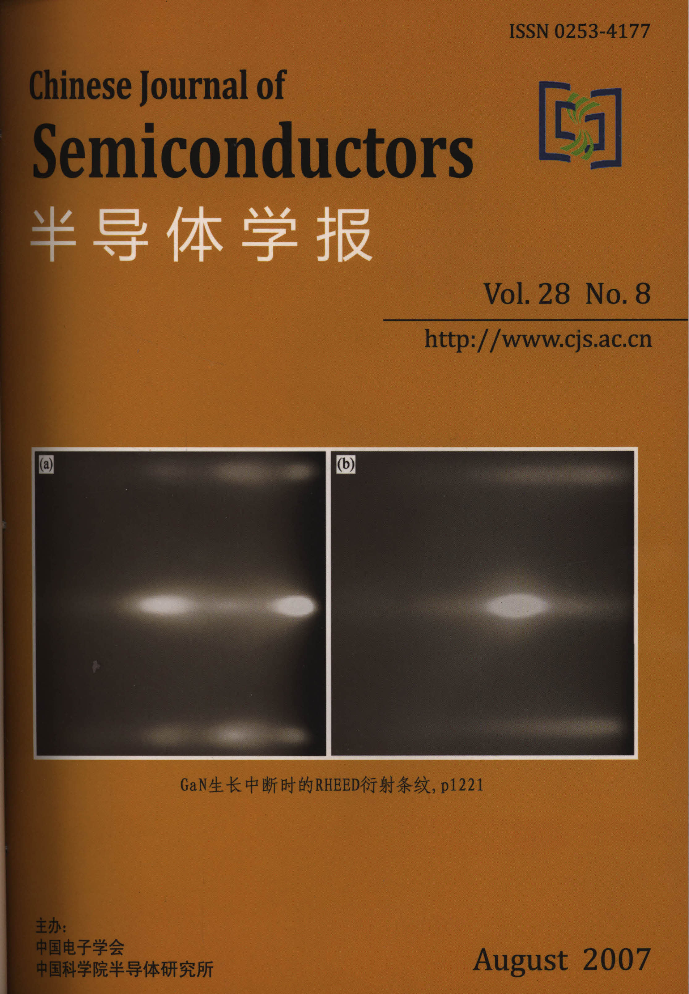
2007, 28(8): 1221-1225
Abstract PDF

GaN layers have been deposited on (0001) sapphire substrates using radio frequency molecular beam epitaxy by In-protected growth interruption modulation.The growth process is monitored by in-situ reflection high-energy electron diffraction.The morphological and structural properties of GaN films are investigated by scanning electron microscopy,atomic force microscopy,and X-ray diffraction (XRD).The results indicate that the density of gallium droplets on the GaN surface is greatly reduced,and the morphology of the GaN films is improved.The RMS is reduced to 0.6nm,while it is 3nm without using this technique.Furthermore,the XRD rocking curves show that the structural quality of the films is superior to that of GaN films formed without using this technique.

GaN layers have been deposited on (0001) sapphire substrates using radio frequency molecular beam epitaxy by In-protected growth interruption modulation.The growth process is monitored by in-situ reflection high-energy electron diffraction.The morphological and structural properties of GaN films are investigated by scanning electron microscopy,atomic force microscopy,and X-ray diffraction (XRD).The results indicate that the density of gallium droplets on the GaN surface is greatly reduced,and the morphology of the GaN films is improved.The RMS is reduced to 0.6nm,while it is 3nm without using this technique.Furthermore,the XRD rocking curves show that the structural quality of the films is superior to that of GaN films formed without using this technique.
Strain and Annealing Effect of SiGe/Si Heterostructure in Limited Area Grown by MBE
Yang Hongbin, Fan Yongliang, Zhang Xiangjiu
Chin. J. Semicond.  2007, 28(8): 1226-1231
Abstract PDF

We report results about the strain and annealing effects for a SiGe/Si structure grown in micron-sized windows by MBE.Experiments show that the strain of the SiGe film in the window is significantly different from that of the film grown on an unpatterned area on the same substrate,the former of which depends not only on the size of the window but also on the stress of the mask material of the window.Experiments also show that the edge effects significantly affect the thermal stability of the Si0.8Ge0.2 film in the window.For Si0.8Ge0.2 film in a window of 3μm×3μm,its strain is relaxed by only less than 4% after the sample is annealed at 950℃ for 30min,which is much less than the strain relaxation of the Si0.8Ge0.2 film grown on the unpatterned area on the same substrate under the same annealing condition.We discuss the possible reasons for these results.

We report results about the strain and annealing effects for a SiGe/Si structure grown in micron-sized windows by MBE.Experiments show that the strain of the SiGe film in the window is significantly different from that of the film grown on an unpatterned area on the same substrate,the former of which depends not only on the size of the window but also on the stress of the mask material of the window.Experiments also show that the edge effects significantly affect the thermal stability of the Si0.8Ge0.2 film in the window.For Si0.8Ge0.2 film in a window of 3μm×3μm,its strain is relaxed by only less than 4% after the sample is annealed at 950℃ for 30min,which is much less than the strain relaxation of the Si0.8Ge0.2 film grown on the unpatterned area on the same substrate under the same annealing condition.We discuss the possible reasons for these results.
Organic Electroluminescent Characteristics of Compound PS∶NPBHole Transporting Layer
Suo Fan, Yu Junsheng, Deng Jing, Lou Shuangling, Jiang Yadong
Chin. J. Semicond.  2007, 28(8): 1232-1236
Abstract PDF

Green organic light-emitting devices with the structure of indium-tin-oxide (ITO)/polystyrene(PS)∶N,N’-bis-(3-naphthyl)-N,N’-biphenyl-(1,1’-biphenyl)-4,4’-diamine (NPB)/tris-(8-hydroxyquinoline)-aluminum (Alq3)/Mg∶Ag were fabricated.A doping system consisting of small-molecular hole transporting material NPB and polymeric matrix polystyrene (PS) was employed as the compound hole transporting layer (HTL),and the thin film preparation was simplified via the spin-coating technique.By adjusting the component ratio of the system,we constructed several devices with different concentration proportions of PS∶NPB.The electroluminescent characteristics of the devices were investigated and discussed.The results demonstrate that the doping concentration of NPB has a remarkable impact on the optoelectric performance of both the HTL and the device.Optimum device performance could be obtained by choosing the best concentration proportion of PS∶NPB to be 1∶1.This contributes to the construction of compound functional layers of OLED devices and to the technical improvement.

Green organic light-emitting devices with the structure of indium-tin-oxide (ITO)/polystyrene(PS)∶N,N’-bis-(3-naphthyl)-N,N’-biphenyl-(1,1’-biphenyl)-4,4’-diamine (NPB)/tris-(8-hydroxyquinoline)-aluminum (Alq3)/Mg∶Ag were fabricated.A doping system consisting of small-molecular hole transporting material NPB and polymeric matrix polystyrene (PS) was employed as the compound hole transporting layer (HTL),and the thin film preparation was simplified via the spin-coating technique.By adjusting the component ratio of the system,we constructed several devices with different concentration proportions of PS∶NPB.The electroluminescent characteristics of the devices were investigated and discussed.The results demonstrate that the doping concentration of NPB has a remarkable impact on the optoelectric performance of both the HTL and the device.Optimum device performance could be obtained by choosing the best concentration proportion of PS∶NPB to be 1∶1.This contributes to the construction of compound functional layers of OLED devices and to the technical improvement.
Preparation of Microcrystalline Silicon Films by Layer-by-Layer Growth Technology and Hydrogen Plasma Treatment on the Stacking Layers in Hot-Wire-Assisted Microwave Electron-Cyclotron-Resonance Chemical Vapor Deposition System
Zeng Tao, Hu Yuehui, Chen Guanghua
Chin. J. Semicond.  2007, 28(8): 1237-1241
Abstract PDF

By introducing layer-by-layer (LBL) growth technology and hydrogen plasma treatment on the stacking layers in a hot-wire-assisted microwave electron-cyclotron-resonance chemical vapor deposition (HW-MWECR CVD) system,we fabricate a series of microcrystalline silicon (μc-Si∶H) films with different thicknesses.It is found that when the thickness of the films is less than 0.55μm,they have the typical characteristics of a-Si∶H films,whose photoconductivity degrades rapidly.But when the film thickness is in the range of 0.60~0.70μm,they have characteristics of both amorphous and microcrystalline silicon films,in which the photoconductivity is very sensitive to changes in thickness,but the decay ratio of the photoconductivity is relatively stable.When the thickness of the films is greater than 0.80μm,they have microcrystalline silicon properties.Moreover,the photoconductivity does not change after simulating illumination for 53.5h.

By introducing layer-by-layer (LBL) growth technology and hydrogen plasma treatment on the stacking layers in a hot-wire-assisted microwave electron-cyclotron-resonance chemical vapor deposition (HW-MWECR CVD) system,we fabricate a series of microcrystalline silicon (μc-Si∶H) films with different thicknesses.It is found that when the thickness of the films is less than 0.55μm,they have the typical characteristics of a-Si∶H films,whose photoconductivity degrades rapidly.But when the film thickness is in the range of 0.60~0.70μm,they have characteristics of both amorphous and microcrystalline silicon films,in which the photoconductivity is very sensitive to changes in thickness,but the decay ratio of the photoconductivity is relatively stable.When the thickness of the films is greater than 0.80μm,they have microcrystalline silicon properties.Moreover,the photoconductivity does not change after simulating illumination for 53.5h.
MSM Ultraviolet Photodetector of Mg0.2Zn0.8O by LMBE
Bi Zhen, Zhang Jingwen, Bian Xuming, Wang Dong, Zhang Xin'+C143an, Hou Xun
Chin. J. Semicond.  2007, 28(8): 1242-1247
Abstract PDF

Mg0.2Zn0.8O films were deposited on the c-plane of sapphire by LMBE with two different structures.The films were all annealed in air at 900℃ for 1h.Then interdigital Al electrodes were evaporated on the films using the standard lift-off technique.A Mg0.2Zn0.8O ultraviolet photodetector was obtained,with a fast rise time of 14.3ns and fall time of 6.5μs.

Mg0.2Zn0.8O films were deposited on the c-plane of sapphire by LMBE with two different structures.The films were all annealed in air at 900℃ for 1h.Then interdigital Al electrodes were evaporated on the films using the standard lift-off technique.A Mg0.2Zn0.8O ultraviolet photodetector was obtained,with a fast rise time of 14.3ns and fall time of 6.5μs.
Effects of Different Collector Current Biases on γ Radiation Response of npn-BJT
Cheng Xinghua, Wang Jian'an, Gong Min, Shi Ruiying, Pu Lin, Liu Luncai, Guo Feng, Yang Chen
Chin. J. Semicond.  2007, 28(8): 1248-1251
Abstract PDF

The total dose effect of γ irradiation at different biased collector currents on Si npn-BJTs was investigated.The experimental results show that the irradiation-induced degradation of an npn-BJT increases with the total dose;however,it decreases with the increase of the collector current at the same total dose.This phenomenon cannot be well explained by the recent space charge model.In this paper,a revised model is presented,in which there are electrically neutral dipoles near the Si-SiO2 interface of the extrinsic base region.By using the new model,all the experimental results have been well interpreted.

The total dose effect of γ irradiation at different biased collector currents on Si npn-BJTs was investigated.The experimental results show that the irradiation-induced degradation of an npn-BJT increases with the total dose;however,it decreases with the increase of the collector current at the same total dose.This phenomenon cannot be well explained by the recent space charge model.In this paper,a revised model is presented,in which there are electrically neutral dipoles near the Si-SiO2 interface of the extrinsic base region.By using the new model,all the experimental results have been well interpreted.
Temperature-Dependent 4H-SiC MOSFET Channel-Electron Mobility Model for Circuit Simulation
Dai Zhenqing, Yang Ruixia, Yang Kewu
Chin. J. Semicond.  2007, 28(8): 1252-1255
Abstract PDF

An improved temperature-dependent 4H-SiC MOSFET channel-electron mobility model for circuit simulation is established.Some factors are introduced,including the effects of temperature on transverse effective electric field and surface roughness scattering,the dependence of the saturation drift velocity of the electron on transverse effective electric field and temperature,and an improved interface trapped charge and fixed oxide charge coulomb scattering model.In addition,the interface state parameters and fixed oxide charge density are extracted by simulation with the experimental temperature-threshold voltage curve.The simulated output characteristic curves with this model agree with experimental results.

An improved temperature-dependent 4H-SiC MOSFET channel-electron mobility model for circuit simulation is established.Some factors are introduced,including the effects of temperature on transverse effective electric field and surface roughness scattering,the dependence of the saturation drift velocity of the electron on transverse effective electric field and temperature,and an improved interface trapped charge and fixed oxide charge coulomb scattering model.In addition,the interface state parameters and fixed oxide charge density are extracted by simulation with the experimental temperature-threshold voltage curve.The simulated output characteristic curves with this model agree with experimental results.
Influence of Gate Voltages on Temperature of LDMOS Under Ultra-High Transient Currents
Li Meizhi, Chen Xingbi
Chin. J. Semicond.  2007, 28(8): 1256-1261
Abstract PDF

The influence of gate voltages on the temperature of LDMOS under ultra-high transient currents is studied.The results show that in comparison with gate-grounded conditions,the temperature in the device rises when the gate voltages are positive,and the temperature falls when the gate voltages are negative.The distributions of the electric fields,conduction currents,and dissipated power densities under different gate voltages are also investigated.It is proved that positive gate voltages weaken the electro-static discharge capability of LDMOS,and negative gate voltages enhance it.These results can be used as a reference for the reliability of power devices.

The influence of gate voltages on the temperature of LDMOS under ultra-high transient currents is studied.The results show that in comparison with gate-grounded conditions,the temperature in the device rises when the gate voltages are positive,and the temperature falls when the gate voltages are negative.The distributions of the electric fields,conduction currents,and dissipated power densities under different gate voltages are also investigated.It is proved that positive gate voltages weaken the electro-static discharge capability of LDMOS,and negative gate voltages enhance it.These results can be used as a reference for the reliability of power devices.
Experiment Results of REBULF LDMOS and Analysis of a Partial n+-Floating Structure
Duan Baoxing, Huang Yongguang, Zhang Bo, Li Zhaoji
Chin. J. Semicond.  2007, 28(8): 1262-1266
Abstract PDF

The results of an experiment on REBULF LDMOS are analyzed.The increased leakage current is due to the n+-floating layer,as proved by the test results of breakdown voltage.However,the breakdown voltage decreases as a result of the leakage current of the n+p junction being exposed to the surface.In order to resolve this problem,a REBULF LDMOS with a partial n+-floating layer is proposed for the first time.An effective REBULF is obtained using this structure,and the large leakage current of Ref.[10] is eliminated by an inner n+p junction around the source.The results show that the breakdown voltage is increased by 60% in comparison with traditional RESURF LDMOS.

The results of an experiment on REBULF LDMOS are analyzed.The increased leakage current is due to the n+-floating layer,as proved by the test results of breakdown voltage.However,the breakdown voltage decreases as a result of the leakage current of the n+p junction being exposed to the surface.In order to resolve this problem,a REBULF LDMOS with a partial n+-floating layer is proposed for the first time.An effective REBULF is obtained using this structure,and the large leakage current of Ref.[10] is eliminated by an inner n+p junction around the source.The results show that the breakdown voltage is increased by 60% in comparison with traditional RESURF LDMOS.
Analytical Model and Optimization of Bulk-Silicon Surface Implanted LDMOS with p Buried Layer
Li Qi, Zhang Bo, Li Zhaoji
Chin. J. Semicond.  2007, 28(8): 1267-1271
Abstract PDF

A novel bulk-silicon surface implanted device with a p buried layer is proposed,and an analytical model for the surface electrical field distributions and breakdown voltage is developed.The on-resistance is decreased as a result of the surface-implanted n+ layer surface,and the p buried layer improves the surface electrical field distribution and increases the optimal drift region doping concentration.Based on the 2D Poisson’s solution,the model gives the closed form solutions of the surface potential and electrical field distributions as functions of the structure parameters and drain bias.The dependence of breakdown voltage on structure parameters is also calculated.Analytical results are well verified by simulation results obtained by MEDICI,showing the validity of the model presented here.BSI structure allowed a significant improvement of breakdown voltage by about 16%,and reduction of on-resistance by about 31%,compared to conventional structures.

A novel bulk-silicon surface implanted device with a p buried layer is proposed,and an analytical model for the surface electrical field distributions and breakdown voltage is developed.The on-resistance is decreased as a result of the surface-implanted n+ layer surface,and the p buried layer improves the surface electrical field distribution and increases the optimal drift region doping concentration.Based on the 2D Poisson’s solution,the model gives the closed form solutions of the surface potential and electrical field distributions as functions of the structure parameters and drain bias.The dependence of breakdown voltage on structure parameters is also calculated.Analytical results are well verified by simulation results obtained by MEDICI,showing the validity of the model presented here.BSI structure allowed a significant improvement of breakdown voltage by about 16%,and reduction of on-resistance by about 31%,compared to conventional structures.
pH Sensor Realized with Standard CMOS Process
Shi Zhaoxia, Zhu Dazhong
Chin. J. Semicond.  2007, 28(8): 1272-1277
Abstract PDF

Based on the conventional sensitive model of an ion-sensitive structure,a threshold voltage model that uses a silicon nitride passivation layer as the sensitive membrane with a multi-floating gate field effect structure has been built.A pH sensor compatible with CMOS is designed according to the 0.6μm CMOS standard process offered by Shanghua.An integrated control circuit keeps the source drain voltage and source drain current of the MFGFET structure in a steady state.Pattern mode noise in the circuit is reduced through a differential output between the ion-sensitive MFGFET and a reference MFGFET.The test result shows the pH sensor has an average sensitivity of 35.8mV/pH from pH 1 to pH 13.

Based on the conventional sensitive model of an ion-sensitive structure,a threshold voltage model that uses a silicon nitride passivation layer as the sensitive membrane with a multi-floating gate field effect structure has been built.A pH sensor compatible with CMOS is designed according to the 0.6μm CMOS standard process offered by Shanghua.An integrated control circuit keeps the source drain voltage and source drain current of the MFGFET structure in a steady state.Pattern mode noise in the circuit is reduced through a differential output between the ion-sensitive MFGFET and a reference MFGFET.The test result shows the pH sensor has an average sensitivity of 35.8mV/pH from pH 1 to pH 13.
A 0.13μm Mixed-Signal CMOS High Speed USB 2.0 Transceiver
Wang Junsong, Zhu Xiaoting, Li Weinan, Hong Zhiliang
Chin. J. Semicond.  2007, 28(8): 1278-1282
Abstract PDF

A USB 2.0 high speed transceiver was designed in 0.13μm mixed-signal CMOS technology.A high-speed current-mode differential comparator,a phase detector with window-enabling logic,and an analog continuously-adjusting CMFB were developed to meet the specifications and 0.13μm technology.The transceiver has been fabricated in SMIC.The transmitter jitter was 53ps,and the bit error rate of the receiver was less than 1e-12.The power consumption was 42.5mW at a power supply of 1.2V, and the chip area was 900μm×700μm.

A USB 2.0 high speed transceiver was designed in 0.13μm mixed-signal CMOS technology.A high-speed current-mode differential comparator,a phase detector with window-enabling logic,and an analog continuously-adjusting CMFB were developed to meet the specifications and 0.13μm technology.The transceiver has been fabricated in SMIC.The transmitter jitter was 53ps,and the bit error rate of the receiver was less than 1e-12.The power consumption was 42.5mW at a power supply of 1.2V, and the chip area was 900μm×700μm.
A Low Voltage Low Power CMOS 5Gb/s Transceiver
Sun Yehui, Jiang Lixin, Qin Shicai
Chin. J. Semicond.  2007, 28(8): 1283-1288
Abstract PDF

A low voltage and low power SerDes transceiver implemented in 0.13μm CMOS is described.The power supply voltage is 1V,and the operating frequency range is from 2.5 to 5GHz.The transmitter includes a 20∶1 serializer and a transmission driver,the latter of which uses pre-emphasis architecture for channel compensation.The receiver employs two 1∶20 deserializer,an input signal pre-amplifier,and a clock and data recovery circuit.The pre-amplifier employs a novel architecture,consisting of a feed-forward equalizer to cancel ISI.The measured transceiver power consumption is 127mW/channel.The RMS jitter of the transmitter output is 4ps.Test results indicate the receiver BER is less than 1e-12 when the input signal amplitude is 150mV differential peak to peak and the eye closure is 0.5UI.

A low voltage and low power SerDes transceiver implemented in 0.13μm CMOS is described.The power supply voltage is 1V,and the operating frequency range is from 2.5 to 5GHz.The transmitter includes a 20∶1 serializer and a transmission driver,the latter of which uses pre-emphasis architecture for channel compensation.The receiver employs two 1∶20 deserializer,an input signal pre-amplifier,and a clock and data recovery circuit.The pre-amplifier employs a novel architecture,consisting of a feed-forward equalizer to cancel ISI.The measured transceiver power consumption is 127mW/channel.The RMS jitter of the transmitter output is 4ps.Test results indicate the receiver BER is less than 1e-12 when the input signal amplitude is 150mV differential peak to peak and the eye closure is 0.5UI.
Research and Design of Wide Input Common-Mode Range Current-Sense Amplifier
Jiang Li, Wu Xiaobo, Yan Xiaolang
Chin. J. Semicond.  2007, 28(8): 1289-1294
Abstract PDF

In order to meet the demand for a wide input common-mode range (ICMR) required by high-side current-sensing amplifiers,input stages whose ICMR can exceed the supply rail were researched and analyzed.Combining the advantages of different circuit structures,a wide ICMR input stage having low input bias current was proposed.With the input stage,a current-sensing amplifier was designed and implemented in a 1.5μm BCD process.It can work at both high and low common mode voltages.The test results show that its ICMR is from 0 to 30V at a 5V supply voltage.Its total output error is below 1.67%.

In order to meet the demand for a wide input common-mode range (ICMR) required by high-side current-sensing amplifiers,input stages whose ICMR can exceed the supply rail were researched and analyzed.Combining the advantages of different circuit structures,a wide ICMR input stage having low input bias current was proposed.With the input stage,a current-sensing amplifier was designed and implemented in a 1.5μm BCD process.It can work at both high and low common mode voltages.The test results show that its ICMR is from 0 to 30V at a 5V supply voltage.Its total output error is below 1.67%.
MEMS Shocking-Acceleration Switch with Threshold Modulating and On-State Latching Function
Jia Mengjun, Li Xinxin, Song Zhaohui, Wang Yuelin
Chin. J. Semicond.  2007, 28(8): 1295-1301
Abstract PDF

Based on the electro-mechanical coupling principle,a shocking-acceleration switch with a threshold adjusting function is presented.The threshold acceleration is set by adjusting the bias voltage.Based on a theoretical analysis for an inertial step-signal,the transient response of the switch in terms of half-sinusoidal,pulsed,and stepped shocking acceleration is simulated using Coventor-Ware.The threshold of the switches ranges from 1000g to 5000g,and the response time is less than 60μs.A fabricated micro-switch array has been tested,resulting in satisfactory switching capability under shocking acceleration,which agrees well with the design.

Based on the electro-mechanical coupling principle,a shocking-acceleration switch with a threshold adjusting function is presented.The threshold acceleration is set by adjusting the bias voltage.Based on a theoretical analysis for an inertial step-signal,the transient response of the switch in terms of half-sinusoidal,pulsed,and stepped shocking acceleration is simulated using Coventor-Ware.The threshold of the switches ranges from 1000g to 5000g,and the response time is less than 60μs.A fabricated micro-switch array has been tested,resulting in satisfactory switching capability under shocking acceleration,which agrees well with the design.
High-Brightness Tapered Diode Lasers Emitting at 980nm with Electrically Separated Ridge Waveguide and Tapered Section
Li Jing, Liu Yuanyuan, Ma Xiaoyu
Chin. J. Semicond.  2007, 28(8): 1302-1306
Abstract PDF

High-brightness tapered diode lasers emitting at 980nm with electrically separated ridge waveguide and tapered section were fabricated.The output power of the tapered section increases with the increase of the ridge waveguide current.An output power of 4.28W,which is the maximum output power with common contacting,is achieved at IRW=150mA.The power-current characteristics remain linear within the studied current range.When the output power of the tapered lasers is 1W,the beam propagation ratio decreases from 3.79 with common contacting to 2.45 with separated contacting.

High-brightness tapered diode lasers emitting at 980nm with electrically separated ridge waveguide and tapered section were fabricated.The output power of the tapered section increases with the increase of the ridge waveguide current.An output power of 4.28W,which is the maximum output power with common contacting,is achieved at IRW=150mA.The power-current characteristics remain linear within the studied current range.When the output power of the tapered lasers is 1W,the beam propagation ratio decreases from 3.79 with common contacting to 2.45 with separated contacting.
Effect of Annealing Temperature on Amorphous Semiconductor As2S8 Film Waveguide
Zou Liner, Chen Baoxue, Du Liping, Liu Xiaoqing, Hamanaka H, Iso M
Chin. J. Semicond.  2007, 28(8): 1307-1311
Abstract PDF

Amorphous semiconductor As2S8 film is shown to undergo structural transformations under thermal machining.Increases in the refractive index and density are found through the application of a prism coupler and Raman spectra.The experimental results demonstrate that the no-full reversible photorefractive phenomenon in the as-deposited and well-illuminated As2S8 film until the annealing temperature reaches 160℃ is found,and depends on the annealing temperature.The full reversible photorefractive phenomenon is observed in annealed As2S8 film after annealing under the glass transition temperature of 130℃.An optical transmission experiment shows that the transmission loss of an amorphous semiconductor As2S8 film after annealing decreases by about 4dB/cm.

Amorphous semiconductor As2S8 film is shown to undergo structural transformations under thermal machining.Increases in the refractive index and density are found through the application of a prism coupler and Raman spectra.The experimental results demonstrate that the no-full reversible photorefractive phenomenon in the as-deposited and well-illuminated As2S8 film until the annealing temperature reaches 160℃ is found,and depends on the annealing temperature.The full reversible photorefractive phenomenon is observed in annealed As2S8 film after annealing under the glass transition temperature of 130℃.An optical transmission experiment shows that the transmission loss of an amorphous semiconductor As2S8 film after annealing decreases by about 4dB/cm.
Influence of ITO Surface Treatment on Performance of Organic Light-Emitting Devices
Wang Jing, Jiang Wenlong, Wang Guangde, Wang Lizhong, Wang Jin, Han Qiang, Ding Guiying, Liu Shiyong
Chin. J. Semicond.  2007, 28(8): 1312-1315
Abstract PDF

ITO anode surfaces are polished with Al2O3.Machine polishing is replaced with an ultrasonic process,which is easier to control to obtain a better ITO anode surface.ITO-coated glass substrates (ITO thickness is 50±10nm,sheet resistance is 40Ω/□) are put into different water-graded Al2O3 polishing solutions with different Al2O3 granularities.Then devices are fabricated with a traditional double-layer structure.The performance of the organic light-emitting diodes (OLEDs) based on the indium tin oxide (ITO) anodes processed ultrasonically in Al2O3 polishing solution is improved.By optimizing the Al2O3 granularity to 0.6μm and the ultrasonic processing time to 10min,the drive voltage falls from 9 to 6V at 100cd/m2 compared with the control device,which underwent no treatment.The luminance of the device is over three times that of the control device,reaching 25880cd/m2 at 15V.The luminous efficiency is 3.82cd/A,which is the best of all the devices.As a result,with an Al2O3 granularity of 0.6μm and ultrasonic processing time of 10min,the electroluminescence performance of the ITO-treated device is improved.The solution-treated sample shows a much smoother surface than the non-treated one,which enhances the hole injection,leading to improved device performance.

ITO anode surfaces are polished with Al2O3.Machine polishing is replaced with an ultrasonic process,which is easier to control to obtain a better ITO anode surface.ITO-coated glass substrates (ITO thickness is 50±10nm,sheet resistance is 40Ω/□) are put into different water-graded Al2O3 polishing solutions with different Al2O3 granularities.Then devices are fabricated with a traditional double-layer structure.The performance of the organic light-emitting diodes (OLEDs) based on the indium tin oxide (ITO) anodes processed ultrasonically in Al2O3 polishing solution is improved.By optimizing the Al2O3 granularity to 0.6μm and the ultrasonic processing time to 10min,the drive voltage falls from 9 to 6V at 100cd/m2 compared with the control device,which underwent no treatment.The luminance of the device is over three times that of the control device,reaching 25880cd/m2 at 15V.The luminous efficiency is 3.82cd/A,which is the best of all the devices.As a result,with an Al2O3 granularity of 0.6μm and ultrasonic processing time of 10min,the electroluminescence performance of the ITO-treated device is improved.The solution-treated sample shows a much smoother surface than the non-treated one,which enhances the hole injection,leading to improved device performance.
A Low Power,Large Dynamic Range 915MHz Passive RFID Tag
Bai Rongrong, Li Yongming, Zhang Chun, Wang Zhihua
Chin. J. Semicond.  2007, 28(8): 1316-1319
Abstract PDF

A 915MHz passive read-only radio frequency identification (RFID) tag compatible with NCITS-256-1999 is presented.This tag has the advantages of low power and large dynamic range.The static current consumption of the analog front-end is 1.6μA under a 1.6V power supply.The minimum RF input power that makes the chip work properly is about 45μW.The tag has been implemented in 0.18μm CMOS technology.Measurement results show that the chip can satisfy the design target well.

A 915MHz passive read-only radio frequency identification (RFID) tag compatible with NCITS-256-1999 is presented.This tag has the advantages of low power and large dynamic range.The static current consumption of the analog front-end is 1.6μA under a 1.6V power supply.The minimum RF input power that makes the chip work properly is about 45μW.The tag has been implemented in 0.18μm CMOS technology.Measurement results show that the chip can satisfy the design target well.
New Modeling and Optimization Method Suitable for UDSM Lithography Simulation
Shen Shanhu, Shi Zheng, Xie Chunlei, Yan Xiaolang
Chin. J. Semicond.  2007, 28(8): 1320-1324
Abstract PDF

This paper presents a novel UDSM lithography process modeling flow using layout contours.The flow mainly includes the following steps:First the transmission cross coefficient matrix standing for the pure optical lithography model is transformed into a much smaller one by circular sampling,while the mask is represented by the same sampling basis;then the resulting system is calibrated half-empirically with the results of a rigorous 3D simulation of the target design layout or the SEM contours.During the model calibration process,novel genetic algorithms are introduced.The experimental results show that the method takes into account new aberration effects,which cannot be simulated well by the traditional method in the UDSM nodes.Due to the fact that the final model is represented using a series of convolution kernels,the constructed model is able to satisfy the speed and accuracy demands of optical proximity correction tasks.

This paper presents a novel UDSM lithography process modeling flow using layout contours.The flow mainly includes the following steps:First the transmission cross coefficient matrix standing for the pure optical lithography model is transformed into a much smaller one by circular sampling,while the mask is represented by the same sampling basis;then the resulting system is calibrated half-empirically with the results of a rigorous 3D simulation of the target design layout or the SEM contours.During the model calibration process,novel genetic algorithms are introduced.The experimental results show that the method takes into account new aberration effects,which cannot be simulated well by the traditional method in the UDSM nodes.Due to the fact that the final model is represented using a series of convolution kernels,the constructed model is able to satisfy the speed and accuracy demands of optical proximity correction tasks.
Kriging Metamodel Based on Genetic Algorithms and Its Application in Analog IC Optimization
You Hailong, Jia Xinzhang, Wang Shaoxi
Chin. J. Semicond.  2007, 28(8): 1325-1329
Abstract PDF

We present a method of constructing the Kriging metamodel of circuits and combining it with genetic algorithms (GA) to optimize a circuit and determine the parameters.Compared with the polynomial regression model,the Kriging model is more suitable to the circuit simulation experiments.Using GA,the problem of the circuit global optimization is solved based on the Kriging metamodel.The method is applied to the optimization design of the band-gap voltage reference,and the result shows that the presented method is effective.

We present a method of constructing the Kriging metamodel of circuits and combining it with genetic algorithms (GA) to optimize a circuit and determine the parameters.Compared with the polynomial regression model,the Kriging model is more suitable to the circuit simulation experiments.Using GA,the problem of the circuit global optimization is solved based on the Kriging metamodel.The method is applied to the optimization design of the band-gap voltage reference,and the result shows that the presented method is effective.