Issue Browser
Volume 29, Issue 12, Dec 2008
Column
LETTERS
Low Noise Distributed Amplifiers Using a Novel Composite-Channel GaN HEMTs
Cheng Zhiqun, Zhou Xiaopeng, Chen J Kevin
J. Semicond.  2008, 29(12): 2297-2300
Abstract PDF

Low noise distributed amplifiers (DAs) using the novel low noise composite-channel Al0.3Ga0.7N/Al0.05Ga0.95N/GaN HEMTs (CC-HEMTs) with 1μm-gate-length are designed and fabricated.Simulated and measured results of the DAs are characterized.The measured results show that the low noise DAs have input and output VSWR (voltage standing wave ratio) of less than 2.0,associated gain of more than 7.0dB and gain ripple of less than 1dB in the frequency range from 2 to 10GHz.Noise figure of the DAs is less than 5dB in the frequency range from 2 to 6GHz,and less than 6.5dB in the frequency range from 2 to 10GHz.The measured results agree well with the simulated ones.

Low noise distributed amplifiers (DAs) using the novel low noise composite-channel Al0.3Ga0.7N/Al0.05Ga0.95N/GaN HEMTs (CC-HEMTs) with 1μm-gate-length are designed and fabricated.Simulated and measured results of the DAs are characterized.The measured results show that the low noise DAs have input and output VSWR (voltage standing wave ratio) of less than 2.0,associated gain of more than 7.0dB and gain ripple of less than 1dB in the frequency range from 2 to 10GHz.Noise figure of the DAs is less than 5dB in the frequency range from 2 to 6GHz,and less than 6.5dB in the frequency range from 2 to 10GHz.The measured results agree well with the simulated ones.
Sampled Grating DBR Lasers with 35nm Quasi-Continuous Tuning Range
Zhang Ruikang, Dong Lei, Wang Dingli, Zhang Jing, Chen Lei, Jiang Shan, Yu Yonglin
J. Semicond.  
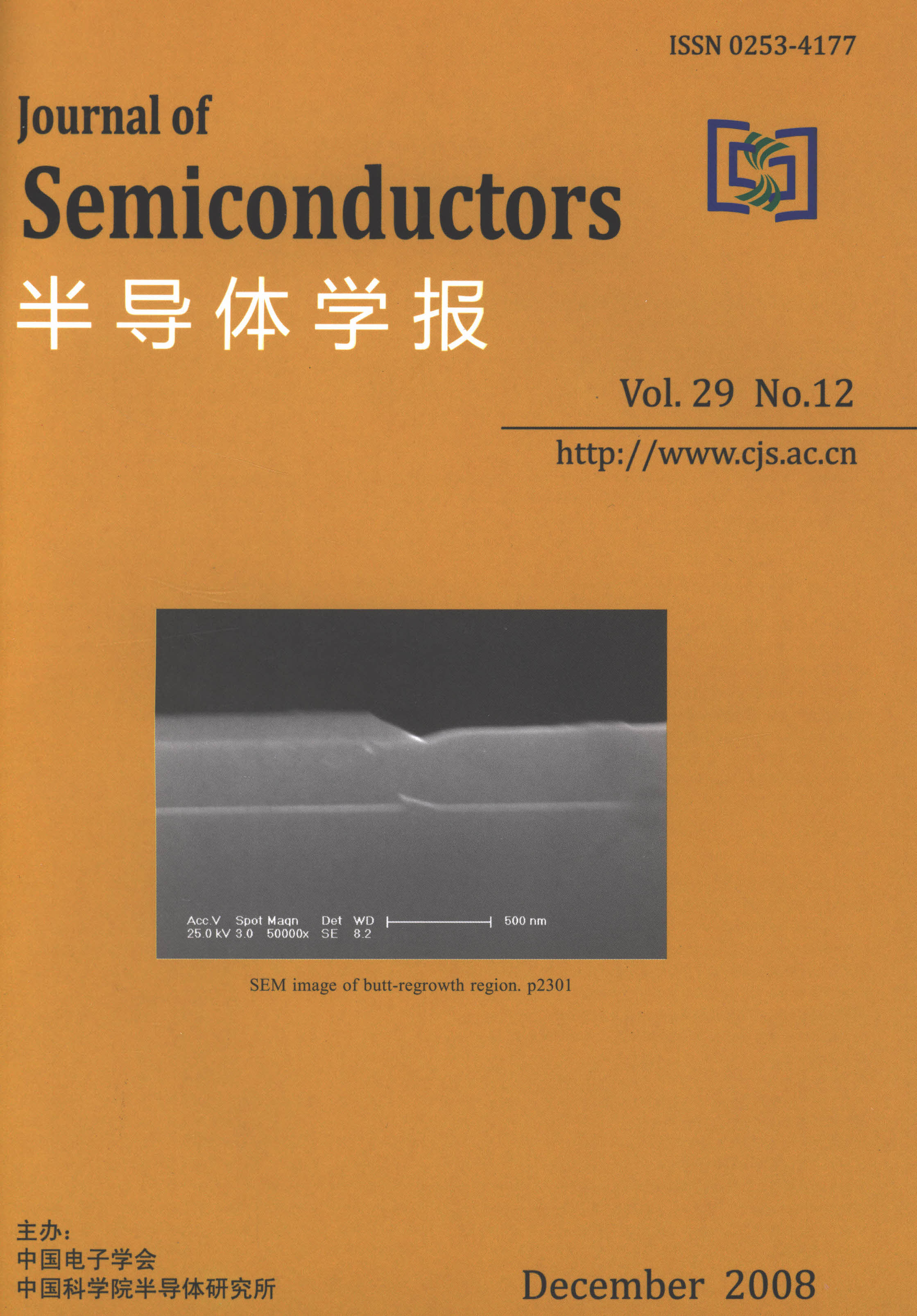
2008, 29(12): 2301-2303
Abstract PDF

We demonstrate a ridge waveguide sampled-grating distributed-feedback laser with quasi-continuous wavelength coverage over a 35nm range.The design is based on a 320nm-thick butt jointed passive waveguide optimized for carrier injection tuning.The butt-joint technology enable optimize the passive waveguide as well as active section.By tuning mirror sections,the laser provides 35nm tuning while maintaining >30dB sidemode suppression ratio.

We demonstrate a ridge waveguide sampled-grating distributed-feedback laser with quasi-continuous wavelength coverage over a 35nm range.The design is based on a 320nm-thick butt jointed passive waveguide optimized for carrier injection tuning.The butt-joint technology enable optimize the passive waveguide as well as active section.By tuning mirror sections,the laser provides 35nm tuning while maintaining >30dB sidemode suppression ratio.
Etching Process of Back-Illuminated ZnO Ultraviolet Focal Plane Array Imagers
Gao Qun, Zhang Jingwen, Hou Xun
J. Semicond.  2008, 29(12): 2304-2306
Abstract PDF

Etching process of back-illuminated ZnO ultraviolet focal plane array imagers was investigated.The etching result of 128×128 array,in which the area of unit cell was 25μm×25μm,was studied.The profile angle was approximately 80°. There was a linear relationship between the etching depth and the etching time.The dependence of etching rate on NH4Cl solution concentration was also studied.The photoresponsivity of the array's unit cells was measured.The UV-to-visible rejection ratio was around 60∶1.

Etching process of back-illuminated ZnO ultraviolet focal plane array imagers was investigated.The etching result of 128×128 array,in which the area of unit cell was 25μm×25μm,was studied.The profile angle was approximately 80°. There was a linear relationship between the etching depth and the etching time.The dependence of etching rate on NH4Cl solution concentration was also studied.The photoresponsivity of the array's unit cells was measured.The UV-to-visible rejection ratio was around 60∶1.
Polymer Arrayed Waveguide Grating with Box-Like Spectral Response
Qin Zhengkun, Ma Chunsheng
J. Semicond.  2008, 29(12): 2307-2310
Abstract PDF

An efficient technique is used to flatten the spectral response of an arrayed waveguide grating (AWG) multiplexer.By subtracting an increment from the core width of odd arrayed waveguides and by adding the same increment to that of even arrayed waveguides,a box-like spectral response can be obtained.A 17×17 polymer AWG multiplexer with box-like spectral response has been made using FPE polymer materials.Measured result for the AWG shows that the box-like spectral response has a 3dB bandwidth of 0.476nm,the crosstalk is about or less than -21dB for every output channel,and the insertion loss is 13~15dB.

An efficient technique is used to flatten the spectral response of an arrayed waveguide grating (AWG) multiplexer.By subtracting an increment from the core width of odd arrayed waveguides and by adding the same increment to that of even arrayed waveguides,a box-like spectral response can be obtained.A 17×17 polymer AWG multiplexer with box-like spectral response has been made using FPE polymer materials.Measured result for the AWG shows that the box-like spectral response has a 3dB bandwidth of 0.476nm,the crosstalk is about or less than -21dB for every output channel,and the insertion loss is 13~15dB.
PAPERS
Structural,Electrical,and Optical Properties of Transparent Conductive Al-Doped ZnO Films Prepared by RF Magnetron Sputtering
Yang Weifeng, Liu Zhuguang, Zhang Feng, Huang Huolin, Wu Zhengyun
J. Semicond.  2008, 29(12): 2311-2315
Abstract PDF

Highly conductive transparent Al-doped zinc oxide (AZO) films with highly (002)-preferred orientation were successfully deposited on glass substrates at room temperature by RF magnetron sputtering.Optimization of deposition parameters was based on sputtering RF power and Ar pressure in the vacuum chamber.AZO films of 180nm with an electrical resistivity as low as 2.68E-3 Ω·cm and an average optical transmission of 90% in the visible range were obtained at RF power of 250W and Ar pressure of 1.2Pa.The effect of chemisorption of oxygen on the grain boundary would capture electrons from conduction band and lead the formation of potential barriers among the crystallites,which will influence the electric property of the AZO thin films.The films have satisfactory properties of low resistance and high transmittance for application as transparent conductive electrodes in light emitting diodes (LEDs) and solar cells.

Highly conductive transparent Al-doped zinc oxide (AZO) films with highly (002)-preferred orientation were successfully deposited on glass substrates at room temperature by RF magnetron sputtering.Optimization of deposition parameters was based on sputtering RF power and Ar pressure in the vacuum chamber.AZO films of 180nm with an electrical resistivity as low as 2.68E-3 Ω·cm and an average optical transmission of 90% in the visible range were obtained at RF power of 250W and Ar pressure of 1.2Pa.The effect of chemisorption of oxygen on the grain boundary would capture electrons from conduction band and lead the formation of potential barriers among the crystallites,which will influence the electric property of the AZO thin films.The films have satisfactory properties of low resistance and high transmittance for application as transparent conductive electrodes in light emitting diodes (LEDs) and solar cells.
Influence of Be-Doping on Electronic Structure and Optical Properties of ZnO
Zheng Yongping, Chen Zhigao, Lu Yu, Wu Qingyun, Weng Zhenzhen, Huang Zhigao
J. Semicond.  2008, 29(12): 2316-2321
Abstract PDF

The electronic structure and optical properties of Zn1-xBexO alloys were studied using first principle calculation based on density functional theory (DTF).The results indicate that the band gap of Zn1-xBexO alloys increases as Be composition increases.The major reason is that the valence band maximum (VBM) of O2p has no obvious shift while the conduction band minimum (CBM) of Zn4s shifts to higher energy as x composition increases.Calculated results of the imaginary part of the dielectric function reveal that the peak heights at 2.0 and 6.76eV decrease as x composition increases,which is attributed to the decrease of the Zn3d states after Be substitutes for Zn.Due to the increasing transition probability from VBM of O2p to CBM of Be2s in wurtzite structure BeO,the peak height at 9.9eV is enhanced and its position shifts toward higher energy.

The electronic structure and optical properties of Zn1-xBexO alloys were studied using first principle calculation based on density functional theory (DTF).The results indicate that the band gap of Zn1-xBexO alloys increases as Be composition increases.The major reason is that the valence band maximum (VBM) of O2p has no obvious shift while the conduction band minimum (CBM) of Zn4s shifts to higher energy as x composition increases.Calculated results of the imaginary part of the dielectric function reveal that the peak heights at 2.0 and 6.76eV decrease as x composition increases,which is attributed to the decrease of the Zn3d states after Be substitutes for Zn.Due to the increasing transition probability from VBM of O2p to CBM of Be2s in wurtzite structure BeO,the peak height at 9.9eV is enhanced and its position shifts toward higher energy.
Preparation of SnS∶Ag Thin Films by Pulse Electrodeposition
Yang Yongli, Cheng Shuying
J. Semicond.  2008, 29(12): 2322-2325
Abstract PDF

SnS:Ag thin films were deposited on ITO by pulse electro-deposition.They were characterized with X-ray diffraction spectroscopy and atomic force microscope.The as-deposited films have a new phase (Ag8SnS6) with good crystallization and big grain size.The conductivity of the films was measured by photoelectrochemical test.It is proved that the SnS:Ag films are p-type of semiconductor.Hall measurement shows that the carrier concentration of the films increases,while their resistivity decreases after Ag-doping.

SnS:Ag thin films were deposited on ITO by pulse electro-deposition.They were characterized with X-ray diffraction spectroscopy and atomic force microscope.The as-deposited films have a new phase (Ag8SnS6) with good crystallization and big grain size.The conductivity of the films was measured by photoelectrochemical test.It is proved that the SnS:Ag films are p-type of semiconductor.Hall measurement shows that the carrier concentration of the films increases,while their resistivity decreases after Ag-doping.
Post-Gate Process Annealing Effects of Recessed AlGaN/GaN HEMTs
Liu Guoguo, Huang Jun, Wei Ke, Liu Xinyu, He Zhijing
J. Semicond.  2008, 29(12): 2326-2330
Abstract PDF

This paper focuses on how to reduce the gate leakage current caused by plasma dry etching.X-ray photoelectron spectroscopy (XPS) is employed to measure the AlGaN surface before and after etching.N vacancies are introduced,which cause that gate currents are not dominated by the thermal electron emission mechanism.N vacancies enhance the tunneling effect and reduce the Schottky barrier height as n-type doped in the etched AlGaN surface.A post-gate process for AlGaN/GaN HEMTs,annealing at 400℃ in a nitrogen ambient for 10min is introduced.After annealing,Ni atoms of gate metal reacted with Ga atoms of AlGaN,and N vacancies were reduced.The reverse leakage decreased by three orders of magnitude,the forward turn-on voltage increased and the ideality factor reduced from 3.07 to 2.08.

This paper focuses on how to reduce the gate leakage current caused by plasma dry etching.X-ray photoelectron spectroscopy (XPS) is employed to measure the AlGaN surface before and after etching.N vacancies are introduced,which cause that gate currents are not dominated by the thermal electron emission mechanism.N vacancies enhance the tunneling effect and reduce the Schottky barrier height as n-type doped in the etched AlGaN surface.A post-gate process for AlGaN/GaN HEMTs,annealing at 400℃ in a nitrogen ambient for 10min is introduced.After annealing,Ni atoms of gate metal reacted with Ga atoms of AlGaN,and N vacancies were reduced.The reverse leakage decreased by three orders of magnitude,the forward turn-on voltage increased and the ideality factor reduced from 3.07 to 2.08.
Power Characteristics of Metamorphic In0.52Al0.48As/In0.6Ga0.4As HEMTs on GaAs Substrates with T-Shaped Gate
Li Ming, Zhang Haiying, Xu Jingbo, Fu Xiaojun
J. Semicond.  2008, 29(12): 2331-2334
Abstract PDF

200nm gate-length power InAlAs/InGaAs MHEMTs with T-shaped gate are characterized for DC,RF,and power performance.The MHEMTs show excellent DC output characteristics with an extrinsic transconductance of 510mS/mm and a threshold voltage of -1.8V.The fT and fmax obtained for the 0.2μm×100μm MHEMTs are 138 and 78GHz,respectively.Power characteristics are obtained under different frequencies.When input power (Pin) is -0.88dBm (or 2.11dBm), the MHEMTs exhibit high power characteristics at 8GHz.Output power (Pout) ,associated gain, power added efficiency (PAE) and density of Pout are 4.05(13.79)dBm,14.9(11.68)dB,67.74(75.1)%,254(239)mW/mm respectively.These promising results are on the path to the application of millimeter wave devices and integrated circuits with improved manufacturability over InP HEMT.

200nm gate-length power InAlAs/InGaAs MHEMTs with T-shaped gate are characterized for DC,RF,and power performance.The MHEMTs show excellent DC output characteristics with an extrinsic transconductance of 510mS/mm and a threshold voltage of -1.8V.The fT and fmax obtained for the 0.2μm×100μm MHEMTs are 138 and 78GHz,respectively.Power characteristics are obtained under different frequencies.When input power (Pin) is -0.88dBm (or 2.11dBm), the MHEMTs exhibit high power characteristics at 8GHz.Output power (Pout) ,associated gain, power added efficiency (PAE) and density of Pout are 4.05(13.79)dBm,14.9(11.68)dB,67.74(75.1)%,254(239)mW/mm respectively.These promising results are on the path to the application of millimeter wave devices and integrated circuits with improved manufacturability over InP HEMT.
259W QCW Al-Free 808nm Linear Laser Diode Arrays
Liu Suping, Zhong Li, Zhang Haiyan, Wang Cuiluan, Feng Xiaoming, Ma Xiaoyu
J. Semicond.  2008, 29(12): 2335-2339
Abstract PDF

Through optimizing the tensile-strained single quantum well (SQW) epitaxial structure and introducing double-channel deep isolation groove etching technologies of linear laser diode arrays,GaAsP/GaInP/AlGaInP SQW separate confinement laser emitting structures are grown by low-pressure metal organic chemical vapor deposition and 1cm-wide laser bars with 50% fill factor are fabricated.The cross sections of the channels are analyzed using scanning electron microscope.Mounted on passively cooled copper heat sinks,the laser bars achieve an output power of 259W in quasi-continuous-wave (200μs pulse width and 2% duty cycles) operation at a driving current of 300A,which is the upper limit of power supply in our measurement setup,and no catastrophically optical mirror damage is observed.A peak power conversion efficiency of 52% is obtained at 104A with 100W output power.At a high-power operation of 100W,the spectrum of the bar has a centric wavelength of 807.8nm and full width at half maximum of 2.4nm.The full angles at half maximum power for fast axis and slow axis are 29.3° and 7.5°,respectively.

Through optimizing the tensile-strained single quantum well (SQW) epitaxial structure and introducing double-channel deep isolation groove etching technologies of linear laser diode arrays,GaAsP/GaInP/AlGaInP SQW separate confinement laser emitting structures are grown by low-pressure metal organic chemical vapor deposition and 1cm-wide laser bars with 50% fill factor are fabricated.The cross sections of the channels are analyzed using scanning electron microscope.Mounted on passively cooled copper heat sinks,the laser bars achieve an output power of 259W in quasi-continuous-wave (200μs pulse width and 2% duty cycles) operation at a driving current of 300A,which is the upper limit of power supply in our measurement setup,and no catastrophically optical mirror damage is observed.A peak power conversion efficiency of 52% is obtained at 104A with 100W output power.At a high-power operation of 100W,the spectrum of the bar has a centric wavelength of 807.8nm and full width at half maximum of 2.4nm.The full angles at half maximum power for fast axis and slow axis are 29.3° and 7.5°,respectively.
Numerical Study of Surface Plasmons Nano-Optical Antenna and Its Array
Guo Baoshan, Song Guofeng, Chen Lianghui
J. Semicond.  2008, 29(12): 2340-2345
Abstract PDF

Nano-rod and bow-tie antennas that are gold nano-antennas on dielectric material and the nano-rod antenna arrays are numerically studied by the finite difference time domain method in three dimensions.The light field that project on the antennas can be confined to a spot with subwavelength width (~λ/11),and the light intensity can be enhanced to 91 times the incident light in the near-field with the bow-tie antenna.The enhancement also exists in the antenna arrays.The highest enhancement of the light intensity at the bow-tie antenna gap can reach about 28000 times,and the localized field can be coupled to a nano-particle near the antenna gap.

Nano-rod and bow-tie antennas that are gold nano-antennas on dielectric material and the nano-rod antenna arrays are numerically studied by the finite difference time domain method in three dimensions.The light field that project on the antennas can be confined to a spot with subwavelength width (~λ/11),and the light intensity can be enhanced to 91 times the incident light in the near-field with the bow-tie antenna.The enhancement also exists in the antenna arrays.The highest enhancement of the light intensity at the bow-tie antenna gap can reach about 28000 times,and the localized field can be coupled to a nano-particle near the antenna gap.
Various Effective Resist Diffusion Lengths Methodology for OPC Model Calibration
Zhu Liang, Wenren Qingqing, Yan Jiang, Gu Yili, Yang Steve
J. Semicond.  2008, 29(12): 2346-2352
Abstract PDF

A various effective resist diffusion lengths methodology for OPC model calibration is proposed,which considers the discrepancy of effective resist diffusion lengths between 1D and 2D patterns.An important step of this methodology is to set up a new calibration flow that lets 1D and 2D patterns have the same optical parameters but different effective diffusion lengths.Furthermore,a design for manufacturing (DFM) interaction is suggested in the calibration flow of the proposed model.From the CD errors of fitting results and the comparison between simulated contours and SEM images,it is found that the various effective resist diffusion lengths model calibration methodology results in a more accurate and stable model.

A various effective resist diffusion lengths methodology for OPC model calibration is proposed,which considers the discrepancy of effective resist diffusion lengths between 1D and 2D patterns.An important step of this methodology is to set up a new calibration flow that lets 1D and 2D patterns have the same optical parameters but different effective diffusion lengths.Furthermore,a design for manufacturing (DFM) interaction is suggested in the calibration flow of the proposed model.From the CD errors of fitting results and the comparison between simulated contours and SEM images,it is found that the various effective resist diffusion lengths model calibration methodology results in a more accurate and stable model.
A Novel High-Speed Equalizer for QAM Signals
Jiang Zhixiang, Zhang Meng, Li Zichuang
J. Semicond.  2008, 29(12): 2353-2358
Abstract PDF

A high-speed equalizer based on a new algorithm:stop-and-go-DD-LMS CMA (SGLMS-CMA) for quadrature amplitude modulation (QAM) signals is presented.It integrates conventional constant modulus algorithm (CMA) and decision-direct least-mean-square (DD-LMS) under stop-and-go principle.Matlab simulations indicate that,compared with conventional CMA,the new algorithm performs five times faster in convergence speed, 3~5dB improved in rudimental mean square error (MSE), 82% decreased in operation complexity and can correct a final phase ambiguity.As to the equalizer block in the system,synthesis results show that the SGLMS-CMA+DD-LMS equalizer's hardware consumption is only 5% greater than the CMA+DD-LMS equalizer's.Finally by using SMIC 0.18μm library to synthesis,the new equalizer is embedded into QAM demodulation chip,and test results show that the new equalizer acts better.

A high-speed equalizer based on a new algorithm:stop-and-go-DD-LMS CMA (SGLMS-CMA) for quadrature amplitude modulation (QAM) signals is presented.It integrates conventional constant modulus algorithm (CMA) and decision-direct least-mean-square (DD-LMS) under stop-and-go principle.Matlab simulations indicate that,compared with conventional CMA,the new algorithm performs five times faster in convergence speed, 3~5dB improved in rudimental mean square error (MSE), 82% decreased in operation complexity and can correct a final phase ambiguity.As to the equalizer block in the system,synthesis results show that the SGLMS-CMA+DD-LMS equalizer's hardware consumption is only 5% greater than the CMA+DD-LMS equalizer's.Finally by using SMIC 0.18μm library to synthesis,the new equalizer is embedded into QAM demodulation chip,and test results show that the new equalizer acts better.
A 10bit 100MS/s Pipelined ADC with an Improved 1.5bit/Stage Architecture
Ye Fan, Shi Yufeng, Guo Yao, Luo Lei, Xu Jun, Ren Junyan
J. Semicond.  2008, 29(12): 2359-2363
Abstract PDF

This paper presents a 10bit 100MS/s CMOS pipelined analog-to-digital converter (ADC) based on an improved 1.5bit/stage architecture.The ADC achieves a peak signal-to-noise-and-distortion ratio (SNDR) of 57dB and maintains 51dB up to 57MHz,the Nyquist frequency for a clock rate of 100Msample/s.The differential non-linearity (DNL) and integral non-linearity (INL) are typically measured as 0.3LSB and 1.0LSB,respectively.The ADC is implemented in a 0.18μm mixed-signal CMOS technology and occupies 0.76mm2.

This paper presents a 10bit 100MS/s CMOS pipelined analog-to-digital converter (ADC) based on an improved 1.5bit/stage architecture.The ADC achieves a peak signal-to-noise-and-distortion ratio (SNDR) of 57dB and maintains 51dB up to 57MHz,the Nyquist frequency for a clock rate of 100Msample/s.The differential non-linearity (DNL) and integral non-linearity (INL) are typically measured as 0.3LSB and 1.0LSB,respectively.The ADC is implemented in a 0.18μm mixed-signal CMOS technology and occupies 0.76mm2.
Temperature and Process Variations Aware Dual Threshold Voltage Footed Domino Circuits Leakage Management
Gong Na, Wang Jinhui, Guo Baozeng, Pang Jiao
J. Semicond.  2008, 29(12): 2364-2371
Abstract PDF

Considering the effect of temperature and process variations, the inputs and clock signals combination sleep state dependent leakage current characteristics is analyzed and the optimal sleep state is examined in sub-65nm dual threshold voltage (Vt) footed domino circuits. HSPICE simulations based on 65nm and 45nm BSIM4 models show that the proposed CLIL state (the clock signal and inputs are all low) is the optimal state to reduce the leakage current of the high fan-in footed domino circuits at high temperature and almost all footed domino circuits at room temperature, as compared to the conventional CHIL state (the clock signal is high and inputs are all low) and the CHIH state (the clock signal and inputs are all high). Further, the influence of the process variations on the leakage current characteristics of the dual Vt footed domino circuits is evaluated. At last, temperature and process variation aware new low leakage current setup guidelines are provided.

Considering the effect of temperature and process variations, the inputs and clock signals combination sleep state dependent leakage current characteristics is analyzed and the optimal sleep state is examined in sub-65nm dual threshold voltage (Vt) footed domino circuits. HSPICE simulations based on 65nm and 45nm BSIM4 models show that the proposed CLIL state (the clock signal and inputs are all low) is the optimal state to reduce the leakage current of the high fan-in footed domino circuits at high temperature and almost all footed domino circuits at room temperature, as compared to the conventional CHIL state (the clock signal is high and inputs are all low) and the CHIH state (the clock signal and inputs are all high). Further, the influence of the process variations on the leakage current characteristics of the dual Vt footed domino circuits is evaluated. At last, temperature and process variation aware new low leakage current setup guidelines are provided.
Preparation and Acetone Sensing Properties of Flower-Like ZnO Nanorods
Liu Li, Feng Yingliang, Yu Lianxiang, Wang Lianyuan, Zhang Tong
J. Semicond.  2008, 29(12): 2372-2375
Abstract PDF

Flower-like ZnO nanorods were prepared with the hydrothermal method and characterized by X-ray diffraction (XRD) and scanning electron microscopy (SEM).The acetone sensing properties of the devices using ZnO films are investigated at different operating temperatures and acetone concentrations.The sensitivity to acetone is the maximum at the operating temperature of 290℃,and the sensor exhibits high sensitivity,rapid response and recovery,excellent stability and reversibility,and prominent selection to common interference gases.

Flower-like ZnO nanorods were prepared with the hydrothermal method and characterized by X-ray diffraction (XRD) and scanning electron microscopy (SEM).The acetone sensing properties of the devices using ZnO films are investigated at different operating temperatures and acetone concentrations.The sensitivity to acetone is the maximum at the operating temperature of 290℃,and the sensor exhibits high sensitivity,rapid response and recovery,excellent stability and reversibility,and prominent selection to common interference gases.
Influences of N2 Flow Rate on the Crystalline Characteristics of GaN Films Deposited on Glass Substrate at Low Temperature
Wang Wenyan, Qin Fuwen, Wu Aimin, Song Shiwei, Liu Ruixian, Jiang Xin, Xu Yin, Gu Biao
J. Semicond.  2008, 29(12): 2376-2380
Abstract PDF

High c-axis oriented GaN films have been deposited on corning 7101 glass substrate by electron cyclotron resonance plasma enhanced metal organic chemical vapor deposition (ECR-PEMOCVD) at low temperature.Influences of N2 flow rate on the crystalline characteristics of the GaN films were investigated by reflection high energy electron diffraction (RHEED) in situ and X-ray diffraction (XRD).And the surface morphology and the optical properties of the GaN film were studied using atomic force microscope (AFM) and room temperature photoluminescence (PL) spectra.The results show that the surface morphology of the GaN film is smooth and its optical peaks are composed of a stronger ultraviolet near band emission and a rather weak green emission.

High c-axis oriented GaN films have been deposited on corning 7101 glass substrate by electron cyclotron resonance plasma enhanced metal organic chemical vapor deposition (ECR-PEMOCVD) at low temperature.Influences of N2 flow rate on the crystalline characteristics of the GaN films were investigated by reflection high energy electron diffraction (RHEED) in situ and X-ray diffraction (XRD).And the surface morphology and the optical properties of the GaN film were studied using atomic force microscope (AFM) and room temperature photoluminescence (PL) spectra.The results show that the surface morphology of the GaN film is smooth and its optical peaks are composed of a stronger ultraviolet near band emission and a rather weak green emission.
Analysis to Microstructure of CuO/SiO2 Composite Thin Films Annealing at Different Atmospheres
Shi Feng, Li Yuguo, Sun Qinjun
J. Semicond.  2008, 29(12): 2381-2384
Abstract PDF

Cu/SiO2 composite thin films were deposited on n-type Si (111) substrates using radio frequency (RF) magnetron co-sputtering method,annealed at high temperature in N2 and NH3 atmosphere,and then cooled and oxidated in the air to form CuO structure.Microstructure of the films was analyzed.The main phase of sample is cubic CuO(200) crystal face and nano-line structure forms with Cu,O elements as the main components to form CuO/SiO2 composite thin films in the sample surface after annealed at 1100℃ in N2 atmosphere.As the annealing temperature increases in NH3 atmosphere,the structure of CuO turns from monoclinic crystal phase to cubic phase and the crystal quality of CuO thin films improves.After annealed at 900 and 1100℃,ordered and scattered micro-particles are formed in samples,and the former is made up of granular clusters with rough surface while the latter is constituted by flake small particles with smooth surface.

Cu/SiO2 composite thin films were deposited on n-type Si (111) substrates using radio frequency (RF) magnetron co-sputtering method,annealed at high temperature in N2 and NH3 atmosphere,and then cooled and oxidated in the air to form CuO structure.Microstructure of the films was analyzed.The main phase of sample is cubic CuO(200) crystal face and nano-line structure forms with Cu,O elements as the main components to form CuO/SiO2 composite thin films in the sample surface after annealed at 1100℃ in N2 atmosphere.As the annealing temperature increases in NH3 atmosphere,the structure of CuO turns from monoclinic crystal phase to cubic phase and the crystal quality of CuO thin films improves.After annealed at 900 and 1100℃,ordered and scattered micro-particles are formed in samples,and the former is made up of granular clusters with rough surface while the latter is constituted by flake small particles with smooth surface.
Effects of NF3 Plasma Treatment Prior to SiN Passivation on the Characteristics of AlGaN/GaN HEMTs
Ren Chunjiang, Chen Tangsheng, Jiao Gang, Chen Gang, Xue Fangshi, Chen Chen
J. Semicond.  2008, 29(12): 2385-2388
Abstract PDF

NF3 plasma surface treatment in inductively coupled plasma (ICP) system prior to SiN passivation on the characteristics of AlGaN/GaN HEMTs has been studied.The results show that current collapse is effectively suppressed while DC and RF performance is not affected for the AlGaN/GaN HEMTs with low power NF3 plasma treated.The AlGaN/GaN HEMT with 6 minutes NF3 plasma treated reaches a power density of 6.15W/mm at 2GHz and 30V operating voltage while the device without NF3 plasma treated only gets an output power density of 1.82W/mm.

NF3 plasma surface treatment in inductively coupled plasma (ICP) system prior to SiN passivation on the characteristics of AlGaN/GaN HEMTs has been studied.The results show that current collapse is effectively suppressed while DC and RF performance is not affected for the AlGaN/GaN HEMTs with low power NF3 plasma treated.The AlGaN/GaN HEMT with 6 minutes NF3 plasma treated reaches a power density of 6.15W/mm at 2GHz and 30V operating voltage while the device without NF3 plasma treated only gets an output power density of 1.82W/mm.
Performance and Design of GaN-Based Transferred-Electron Devices
Shao Xianjie, Lu Hai, Zhang Rong, Zheng Youdou, Li Zhonghui
J. Semicond.  2008, 29(12): 2389-2392
Abstract PDF

Based on the basic transit-time domain operation mode of TEDs,we first calculated the ideal maximum oscillation frequency of GaN-based transferred-electron devices (TEDs),which can be as high as 4.7THz.This value is nearly 8 times as high as that of GaAs-based TEDs,which is about 0.6 THz.Next,we calculated the maximum output power of GaN-based TEDs indicating that GaN-based TEDs are promising for high microwave power applications.We also discussed the two critical conditions in GaN-based design for generating stable Gunn oscillations in transit-time domain mode.Our calculation indicates that the product of electron concentration and the length of active layer should be higher than a critical value of 6.3E12cm-2 ;and the doping lever of the active layer has to be smaller than a critical level of 3.2E17cm-3.This study suggests that GaN-based TEDs have significant advantages for high-frequency and high-power microwave generation,which are perspective for high-power THz signal source applications.

Based on the basic transit-time domain operation mode of TEDs,we first calculated the ideal maximum oscillation frequency of GaN-based transferred-electron devices (TEDs),which can be as high as 4.7THz.This value is nearly 8 times as high as that of GaAs-based TEDs,which is about 0.6 THz.Next,we calculated the maximum output power of GaN-based TEDs indicating that GaN-based TEDs are promising for high microwave power applications.We also discussed the two critical conditions in GaN-based design for generating stable Gunn oscillations in transit-time domain mode.Our calculation indicates that the product of electron concentration and the length of active layer should be higher than a critical value of 6.3E12cm-2 ;and the doping lever of the active layer has to be smaller than a critical level of 3.2E17cm-3.This study suggests that GaN-based TEDs have significant advantages for high-frequency and high-power microwave generation,which are perspective for high-power THz signal source applications.
Poly-Si Film Functional Layer Based AM-OLED Display Panel
Li Yang, Zhao Shuyun, Wu Chunya, Meng Zhiguo, Wang Yi, Xiong Shaozhen
J. Semicond.  2008, 29(12): 2393-2397
Abstract PDF

In the active matrix addressing organic light--emitting diode (AM-OLED) display panel,we modify electricity functional layer-layout of the poly-Si thin film transistor (TFT) and prolong the source and drain electrode as the anode of OLED,forming the micro cavity AM-OLED with a certain quality factor (Q).The slight modification of the layout can not only improve the color saturation of the OLED,which is good to display color image,but also omit the process of deposition and photo lithography of OLED's ITO anode.As a result,p+-MIC poly-Si thin film optic functional layer is formed.The thickness of optic functional layer is optimized;and the electricity characteristic of TFT and the optic characteristic of OLED are compared.When the thickness is 40nm,μFE (cm2/(V·s)),Vth(V),S(V/decade),Ion/Ioff(1E7) at |Vds|=-5V,GIDL (pA/μm ) at Vds=-5V and Vg=5V of TFT are very good, and display device (MOLED) with high EL intensity and high saturation performance could be realized.This not only develops the high performance of red MOLED but also greatly results simplification of the preparation process flow.

In the active matrix addressing organic light--emitting diode (AM-OLED) display panel,we modify electricity functional layer-layout of the poly-Si thin film transistor (TFT) and prolong the source and drain electrode as the anode of OLED,forming the micro cavity AM-OLED with a certain quality factor (Q).The slight modification of the layout can not only improve the color saturation of the OLED,which is good to display color image,but also omit the process of deposition and photo lithography of OLED's ITO anode.As a result,p+-MIC poly-Si thin film optic functional layer is formed.The thickness of optic functional layer is optimized;and the electricity characteristic of TFT and the optic characteristic of OLED are compared.When the thickness is 40nm,μFE (cm2/(V·s)),Vth(V),S(V/decade),Ion/Ioff(1E7) at |Vds|=-5V,GIDL (pA/μm ) at Vds=-5V and Vg=5V of TFT are very good, and display device (MOLED) with high EL intensity and high saturation performance could be realized.This not only develops the high performance of red MOLED but also greatly results simplification of the preparation process flow.
Effect of the Interfacial Nanoparticles on Organic Cross-Point Memory
Sun Yedan, Li Yun, Qiu Danfeng, Cao Liqiang, Pan Lijia, Pu Lin, Shi Yi
J. Semicond.  2008, 29(12): 2398-2402
Abstract PDF

We investigate the electrical performance of cross point bistable memory affected by the nanoparticles formed at the organic/electrode interface.The middle medium is 2-amino-4,5-dicyanoimidazole (AIDCN) film fabricated by vacuum evaporation,and the anode and cathode metals of the device are ITO glass and Al,respectively.The microstructure features of the SnOx nanoparticles,which were formed due to the chemical reaction between the tin oxide in ITO and AIDCN,have been investigated using transition electron microscopy (TEM) and X-ray photoelectron spectrum (XPS),etc.The tin element at the AIDCN/ITO interface mainly arises from the tin segregation layer near the surface of ITO.It is demonstrated that the interface of ITO and AIDCN is of the crucial importance of the electrical behavior.Through this kind of in-situ reaction at an interface,a cross point memory with on-off ratio over 1E11 orders are obtained.

We investigate the electrical performance of cross point bistable memory affected by the nanoparticles formed at the organic/electrode interface.The middle medium is 2-amino-4,5-dicyanoimidazole (AIDCN) film fabricated by vacuum evaporation,and the anode and cathode metals of the device are ITO glass and Al,respectively.The microstructure features of the SnOx nanoparticles,which were formed due to the chemical reaction between the tin oxide in ITO and AIDCN,have been investigated using transition electron microscopy (TEM) and X-ray photoelectron spectrum (XPS),etc.The tin element at the AIDCN/ITO interface mainly arises from the tin segregation layer near the surface of ITO.It is demonstrated that the interface of ITO and AIDCN is of the crucial importance of the electrical behavior.Through this kind of in-situ reaction at an interface,a cross point memory with on-off ratio over 1E11 orders are obtained.
Mechanism of Energy-Injection Damage of Silicon Bipolar Low-Noise Amplifiers
Chai Changchun, Yang Yintang, Zhang Bing, Leng Peng, Yang Yang, Rao Wei
J. Semicond.  2008, 29(12): 2403-2407
Abstract PDF

Experiments of the energy injection into silicon bipolar low-noise amplifiers (LNA) are conducted by introducing pulse-modulated 150MHz radio frequency (RF) signal at LNAs inputs.The results show that the noise figure and the gain characteristic of silicon LNAs are sensitive to the injection energy.The metallization damage between the base and the emitter is correlated with the energy injection from the sample dissection analysis.The noise figure increases due to increased metal-semiconductor contact resistance of the base.The gain of the LNAs also increases with injection energy following the positive drift damage model of hFE for the silicon bipolar devices.Therefore,the traditional way to evaluate the damage effect of devices and circuits simply by the change of the gain is not comprehensive due to the complexity of the energy injection induced damage.

Experiments of the energy injection into silicon bipolar low-noise amplifiers (LNA) are conducted by introducing pulse-modulated 150MHz radio frequency (RF) signal at LNAs inputs.The results show that the noise figure and the gain characteristic of silicon LNAs are sensitive to the injection energy.The metallization damage between the base and the emitter is correlated with the energy injection from the sample dissection analysis.The noise figure increases due to increased metal-semiconductor contact resistance of the base.The gain of the LNAs also increases with injection energy following the positive drift damage model of hFE for the silicon bipolar devices.Therefore,the traditional way to evaluate the damage effect of devices and circuits simply by the change of the gain is not comprehensive due to the complexity of the energy injection induced damage.
Inductively Coupled Plasma via Hole Etching of AlGaN/GaN HEMTs on SiC Substrate
Ren Chunjiang, Chen Tangsheng, Bai Song, Xu Xiaole, Jiao Gang, Chen Chen
J. Semicond.  2008, 29(12): 2408-2411
Abstract PDF

AlGaN/GaN HEMTs on SiC substrate were fabricated and through-wafer via holes up to 50μm deep were etched by inductively coupled plasma (ICP).The SiC substrate was thinned to 50μm,and 3μm thick Ni mask with openings was patterned followed by SF6/O2 gas mixture etching of SiC substrate.Through-wafer via holes with a slightly sloped via sidewall to facilitate subsequent metal coverage to complete the front-to-back electrical connection were finished by Cl2/BCl3 gas mixture based ICP etching of AlGaN/GaN heterostructure.The method exhibited is suitable for AlGaN/GaN HEMTs and MMICs fabrication.

AlGaN/GaN HEMTs on SiC substrate were fabricated and through-wafer via holes up to 50μm deep were etched by inductively coupled plasma (ICP).The SiC substrate was thinned to 50μm,and 3μm thick Ni mask with openings was patterned followed by SF6/O2 gas mixture etching of SiC substrate.Through-wafer via holes with a slightly sloped via sidewall to facilitate subsequent metal coverage to complete the front-to-back electrical connection were finished by Cl2/BCl3 gas mixture based ICP etching of AlGaN/GaN heterostructure.The method exhibited is suitable for AlGaN/GaN HEMTs and MMICs fabrication.
Rule of Oxidation Rate in Vertical Cavity Surface Emitting Lasers
Feng Yuan, Zhong Jingchang, Hao Yongqin, Zhao Yingjie, Hou Lifeng, Yao Yanping
J. Semicond.  2008, 29(12): 2412-2416
Abstract PDF

This research is based on the selective oxidation experiments under different conditions,in which the microstructure pictures and the component contents of the produced oxide in different depths are obtained.The oxidation rate is mainly controlled by diffusion;therefore,the experimental results are analyzed with the kinetics of thermal diffusion.It shows that the results of mathematical derivation are basically in agreement with the experimental results.Thus it is concluded that the concentration of oxidant is exponentially declined as the depth of oxidation in vertical cavity surface emitting lasers increases.

This research is based on the selective oxidation experiments under different conditions,in which the microstructure pictures and the component contents of the produced oxide in different depths are obtained.The oxidation rate is mainly controlled by diffusion;therefore,the experimental results are analyzed with the kinetics of thermal diffusion.It shows that the results of mathematical derivation are basically in agreement with the experimental results.Thus it is concluded that the concentration of oxidant is exponentially declined as the depth of oxidation in vertical cavity surface emitting lasers increases.
Low-Voltage and High Efficiency Tandem White Organic Light Emitting Diodes
Wei Fuxiang, Fang Liang, Jiang Xueyin, Zhang Zhilin
J. Semicond.  2008, 29(12): 2417-2420
Abstract PDF

We report a white tandem organic light-emitting device (TOLED) with high efficiency and low drive voltage using Bphen:Li/WO3 as the interconnecting layer.The TOLED have been fabricated by connecting two low-voltage driving white units with conductive transport layers.The tandem two-unit device produces two higher luminance efficiency than that expected of a single-unit device.A maximum efficiency of 17cd/A is achieved by the tandem device comprised of two white-fluorescent OLEDs.The power efficiency of tandem white organic light-emitting device is enhanced by 53% as compared to the control device.

We report a white tandem organic light-emitting device (TOLED) with high efficiency and low drive voltage using Bphen:Li/WO3 as the interconnecting layer.The TOLED have been fabricated by connecting two low-voltage driving white units with conductive transport layers.The tandem two-unit device produces two higher luminance efficiency than that expected of a single-unit device.A maximum efficiency of 17cd/A is achieved by the tandem device comprised of two white-fluorescent OLEDs.The power efficiency of tandem white organic light-emitting device is enhanced by 53% as compared to the control device.
Experimental Study on Solar Cell Arrays of Trough Concentrating Solar System
Xu Yongfeng, Li Ming, Wang Liuling, He Jianhua, Zhang Xinghua, Wang Yunfeng, Xiang Ming
J. Semicond.  2008, 29(12): 2421-2426
Abstract PDF

A series experiment works have been done with single crystalline silicon solar cell array,polysilicon solar cell array,super cell array and GaAs cell array through the trough concentrating solar system.The experimental results show that the I-V curve of the crystalline silicon,polysilicon and super cell arrays are beeline in the concentrating solar irradiance,which reduce the efficiency and decrease the output power.However the I-V curve of GaAs cell array is very good in the concentrating solar irradiance,the efficiency of GaAs cell array increases from 23.66% to 26.50%,and the output of GaAs magnifies 12 times.So it is considerable to improve the efficiency if the GaAs cell has been adopted in the concentrating PV system.The temperature coefficients of Pm,FF and η of GaAs cell array are -0.12W/K,-0.10%/K,and -0.21%/K.In order to keep better efficiency,the forced cooling must be applied.At the same time,the quantity of heat can been recovered for using.All those work are benefits to further study in improving the efficiency of trough concentrating solar system and cosmically making use of concentrating PV system.

A series experiment works have been done with single crystalline silicon solar cell array,polysilicon solar cell array,super cell array and GaAs cell array through the trough concentrating solar system.The experimental results show that the I-V curve of the crystalline silicon,polysilicon and super cell arrays are beeline in the concentrating solar irradiance,which reduce the efficiency and decrease the output power.However the I-V curve of GaAs cell array is very good in the concentrating solar irradiance,the efficiency of GaAs cell array increases from 23.66% to 26.50%,and the output of GaAs magnifies 12 times.So it is considerable to improve the efficiency if the GaAs cell has been adopted in the concentrating PV system.The temperature coefficients of Pm,FF and η of GaAs cell array are -0.12W/K,-0.10%/K,and -0.21%/K.In order to keep better efficiency,the forced cooling must be applied.At the same time,the quantity of heat can been recovered for using.All those work are benefits to further study in improving the efficiency of trough concentrating solar system and cosmically making use of concentrating PV system.
A Decoupled Silicon Micromachined Gyroscope with Vibration Isolation Frame
Xiao Dingbang, Wu Xuezhong, Li Weidong, Dong Peitao, Hou Zhanqiang, Li Shengyi
J. Semicond.  2008, 29(12): 2427-2431
Abstract PDF

A decoupled silicon micromachined gyroscope with vibration isolation frame is introduced.This structure employs independent suspension beams and inertial masses for the drive and sense modes.The drive and sense structures are separated by the vibration isolation frame,so the cross-coupling between the modes is reduced.The gyroscope is fabricated on the n-type 〈100〉 wafer using TMAH wet-etching and DRIE,and its read-out circuit is designed.Test results show that the frequencies of the drive and sense modes are 2.981 and 2.813kHz,and the quality factors of the drive and sense modes are 800 and 34.The scale factor is measured as 38mV/(°/s) with a nonlinearity of 0.8%.The short-term bias stability of this gyroscope in half an hour is 0.28°/s.

A decoupled silicon micromachined gyroscope with vibration isolation frame is introduced.This structure employs independent suspension beams and inertial masses for the drive and sense modes.The drive and sense structures are separated by the vibration isolation frame,so the cross-coupling between the modes is reduced.The gyroscope is fabricated on the n-type 〈100〉 wafer using TMAH wet-etching and DRIE,and its read-out circuit is designed.Test results show that the frequencies of the drive and sense modes are 2.981 and 2.813kHz,and the quality factors of the drive and sense modes are 800 and 34.The scale factor is measured as 38mV/(°/s) with a nonlinearity of 0.8%.The short-term bias stability of this gyroscope in half an hour is 0.28°/s.
A Nodal Analysis Method for Electrically Actuated Bow-tie Shaped Fixed-Fixed Beams
Li Min, Huang Qing'an, Li Weihua
J. Semicond.  2008, 29(12): 2432-2436
Abstract PDF

In order to perform mixed-domain simulation of electrically actuated bow-tie shaped fixed-fixed beams,the governing equations treatment for trapeziform beam elements under electrostatic load was carried out based on a Galerkin residual method.The nodal model for the trapeziform beam and corresponding equivalent circuit is developed by HSpice.It proves accurate in comparison with FEA results and experiment results given by the Reference.

In order to perform mixed-domain simulation of electrically actuated bow-tie shaped fixed-fixed beams,the governing equations treatment for trapeziform beam elements under electrostatic load was carried out based on a Galerkin residual method.The nodal model for the trapeziform beam and corresponding equivalent circuit is developed by HSpice.It proves accurate in comparison with FEA results and experiment results given by the Reference.
MMIC-Based RF On-Chip LC Passive Filters
Wu Rui, Liao Xiaoping, Zhang Zhiqiang
J. Semicond.  2008, 29(12): 2437-2442
Abstract PDF

The design and fabrication of on-chip LC low/band-pass filters are presented,and the filters are accomplished with MMIC process.Measurement results show that the Q of a 3nH inductor is 13.8 at 6.8GHz and the self-resonant frequency is 15.5GHz.The measured cutoff/center frequencies of low/band-pass filters agree with the design,and the contrast are 2% and 3.3% respectively.The insertion loss of low-pass filters is less than 3dB,and the insertion loss of band-pass filter is 7.2dB at the center frequency.

The design and fabrication of on-chip LC low/band-pass filters are presented,and the filters are accomplished with MMIC process.Measurement results show that the Q of a 3nH inductor is 13.8 at 6.8GHz and the self-resonant frequency is 15.5GHz.The measured cutoff/center frequencies of low/band-pass filters agree with the design,and the contrast are 2% and 3.3% respectively.The insertion loss of low-pass filters is less than 3dB,and the insertion loss of band-pass filter is 7.2dB at the center frequency.
Design of pn Mixed Pull-Down Network Domino XOR Gate in 45nm Technology
Wang Jinhui, Gong Na, Geng Shuqin, Hou Ligang, Wu Wuchen, Dong Limin
J. Semicond.  2008, 29(12): 2443-2448
Abstract PDF

A pn mixed pull-down network technique is proposed, based on the application of pMOS transistor and nMOS transistor in the pull-down network,to lower the power and improve the performance of the domino circuits.First,a domino XOR gate with this technique is designed.Compared to the standard N type domino XOR gate,its static power and dynamic power are reduced by up to 46% and 3%,respectively.Second,using this technique,the dual-threshold voltage techniques and the multiple supply voltages techniques,a novel domino XOR gate is present and its static power and dynamic power are reduced by up to 82% and 21%,as compared to the standard N type domino XOR gate.At last,the minimum static power state of four XOR gates and AC noise margins are analyzed and obtained thoroughly.

A pn mixed pull-down network technique is proposed, based on the application of pMOS transistor and nMOS transistor in the pull-down network,to lower the power and improve the performance of the domino circuits.First,a domino XOR gate with this technique is designed.Compared to the standard N type domino XOR gate,its static power and dynamic power are reduced by up to 46% and 3%,respectively.Second,using this technique,the dual-threshold voltage techniques and the multiple supply voltages techniques,a novel domino XOR gate is present and its static power and dynamic power are reduced by up to 82% and 21%,as compared to the standard N type domino XOR gate.At last,the minimum static power state of four XOR gates and AC noise margins are analyzed and obtained thoroughly.