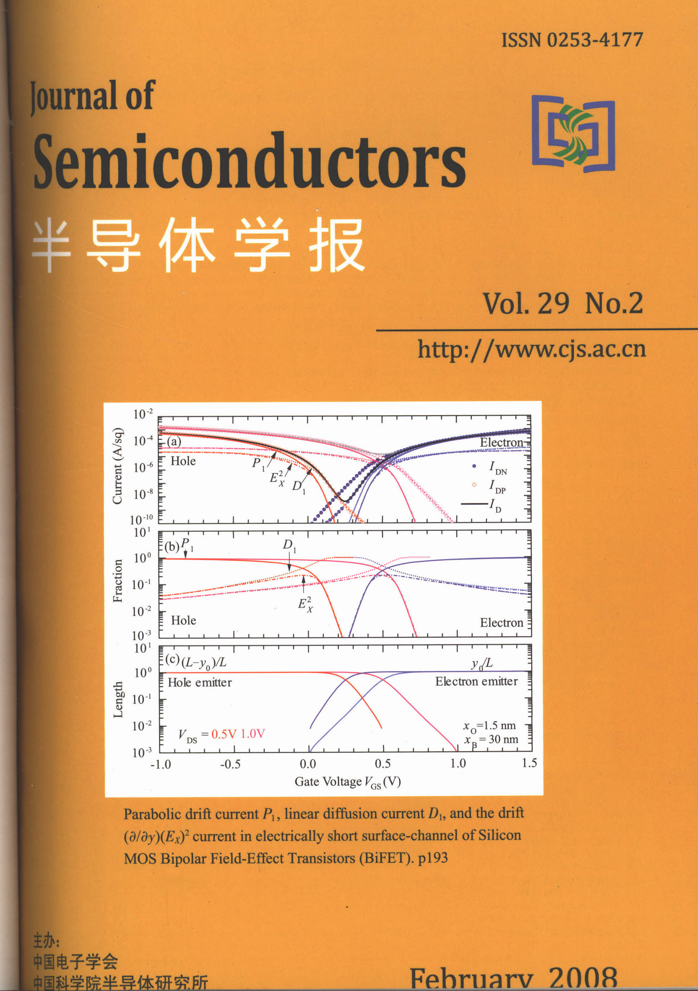
This paper gives the short channel analytical theory of the bipolar field-effect transistor (BiFET) with the drift and diffusion currents separately computed in the analytical theory. As in the last-month paper which represented the drift and diffusion current by the single electrochemical (potential-gradient) current, the two-dimensional transistor is partitioned into two sections, the source and drain sections, each can operate as the electron or hole emitter or collector under specific combinations of applied terminal voltages. Analytical solution is then obtained in the source and drain sections by separating the two-dimensional trap-free Shockley Equations into two one-dimensional equations parametrically coupled via the surface-electric-potential and by using electron current continuity and hole current continuity at the boundary between the emitter and collector sections. Total and the drift and diffusion components of the electron-channel and hole-channel currents and output and transfer conductances, and the electrical lengths of the two sections are computed and presented in graphs as a function of the D.C.terminal voltages for the model transistor with two identical and connected metal-oxide-silicon-gates (MOS-gates) on a thin pure-silicon base over practical ranges of thicknesses of the silicon base and gate oxide. Deviations of the two-section short-channel theory from the one-section long-channel theory are described.
We report a new method for calculating transmission coefficients across arbitrary potential barriers based on the Runge-Kutta method.A numerical solution of the Schrdinger equation is calculated using the Runge-Kutta method, and a new model is established to analyze the numerical results to find the transmission coefficient.This technique is applied to various cases, such as parabolic potential barrier and double-barrier structures.Transmission probability with high precision is obtained and discussed.The tunnelling current density through a MOS structure is also explored and the result coincides with the Fowler-Nordheim model, which indicates the applicability of our method.
A model is presented to describe a compensation mechanism for semi-insulating 6H-SiC grown with the intentional doping of vanadium.Because we found nitrogen to be the principal shallow donor impurity in SiC by secondary ion mass spectroscopy (SIMS) measurements, semi-insulating properties in SiC are achieved by compensating the nitrogen donor with the vanadium deep acceptor level.The presence of different vanadium charge states V3+ and V4+ is detected by electron paramagnetic resonance and optical absorption measurements, which coincides with the results obtained by SIMS measurements.Both optical absorption and low temperature photoluminescence measurements reveal that the vanadium acceptor level is located at 0.62eV below the conduction band in 6H-SiC.
GaN nanorods are successfully synthesized on Si(111) substrates with magnetron sputtering through ammoniating Ga2O3/Co films at 950℃.X-ray diffraction, scanning electron microscopy, high-resolution transmission electron microscopy, and Fourier-transform infrared spectroscopy are used to characterize the samples.The results demonstrate that the nanorods are single-crystal GaN with a hexagonal wurtzite structure and possess relatively smooth surfaces.The growth mechanism of GaN nanorods is also discussed.
The on-resistance degradations of the p-type lateral extended drain MOS transistor (pLEDMOS) with thick gate oxide under different hot carrier stress conditions are different, which has been experimentally investigated.This difference results from the interface trap generation and the hot electron injection, and trapping into the thick gate oxide and field oxide of the pLEDMOS transistor.An improved method to reduce the on-resistance degradations is also presented, which uses the field oxide as the gate oxide instead of the thick gate oxide.The effects are analyzed with a MEDICI simulator.
A novel capacitive biaxial microaccelerometer with a highly symmetrical microstructure is developed.The sensor is composed of a single seismic mass, grid strip, supporting beam, joint beam, and damping adjusting combs.The sensing method of changing capacitance area is used in the design, which depresses the requirement of the DRIE process, and decreases electronic noise by increasing sensing voltage to improve the resolution.The parameters and characteristics of the biaxial microaccelerometer are discussed with the FEM tool ANSYS.The simulated results show that the transverse sensitivity of the sensor is equal to zero.The testing devices based on the slide-film damping effect are fabricated, and the testing quality factor is 514, which shows that the designed structure can improve the resolution and proves the feasibility of the designed process.
A programmable multi-modulus frequency divider is designed and implemented in a 0.35μm CMOS process.The multi-modulus frequency divider is a single chip with two dividers in series, which are divided by 4 or 5 prescaler and by 128~255 multi-modulus frequency divider.In the circuit design, power and speed trade-offs are analyzed for the prescaler, and power optimization techniques are used according to the input frequency of each divider cell for the 128~255 multi-modulus frequency divider.The chip is designed with ESD protected I/O PAD.The dividers chain can work as high as 2.4GHz with a single ended input signal and beyond 2.6GHz with differential input signals.The dual-modulus prescaler consumes 11mA of current while the 128~255 multi-modulus frequency divider consumes 17mA of current with a 3.3V power supply.The core area of the die without PAD is 0.65mm×0.3mm.This programmable multi-modulus frequency divider can be used for 2.4GHz ISM band PLL-based frequency synthesizers.To our knowledge, this is the first reported multi-modulus frequency divider with this structure in China.
A novel macro-model of high-voltage DMOS for power ICs is proposed according to the canonical piecewise-linear model technique.The method describes nonlinear characteristics directly as functions of node voltage.We employ the Powell algorithm, which gives higher accuracy without the convergence problem and with lower analysis time.Finally, a comparison of simulation results and measurement results in application to power ICs is reported.
We investigate the binding energies of excitons in a strained (111)-oriented zinc-blende GaN/Al0.3Ga0.7N quantum well screened by the electron-hole (e-h) gas under hydrostatic pressure by combining a variational method and a self-consistent procedure.A built-in electric field produced by the strain-induced piezoelectric polarization is considered in our calculations.The result indicates that the binding energies of excitons increase nearly linearly with pressure, even though the modification of strain with hydrostatic pressure is considered, and the influence of pressure is more apparent under higher e-h densities.It is also found that as the density of an e-h gas increases, the binding energies first increase slowly to a maximum and then decrease rapidly when the e-h density is larger than about 1e11cm-2.The excitonic binding energies increase obviously as the barrier thickness decreases due to the decrease of the built-in electric field.
Deep level transient Fourier spectroscopy (DLTFS) measurements are used to characterize the deep impurity levels in n-type 4H-SiC by vanadium ions implantation.Two acceptor levels of vanadium at EC-0.81 and EC-1.02eV with the electron capture cross section of 7.0e-16 and 6.0e-16 cm2 are observed, respectively.Low-temperature photoluminescence measurements in the range of 1.4~3.4eV are also performed on the sample, which reveals the formation of two electron traps at 0.80 and 1.16eV below the conduction band.These traps indicate that vanadium doping leads to the formation of two deep acceptor levels in 4H-SiC, with the location of 0.8±0.01 and 1.1±0.08eV below the conduction band.
We study the problem of multiple node upset (MNU) using three-dimensional device simulation.The results show the transient floating node and charge lateral diffusion are the key reasons for MNU.We compare the MNU with multiple bit upset (MBU), and find that their characteristics are different.Methods to avoid MNU are also discussed.
A 4.224GHz quadrature voltage-controlled oscillator (QVCO) applied in MB-OFDM UWB synthesizers is implemented in 0.18μm RF-CMOS technology.An improved structure of the QVCO is presented for better phase noise.A novel configuration of a MOS varactor is designed for good linearity of Kvco, as well as a new digital capacitor controlled array topology with lower parasitic capacitance and lower Ron.Measurement results show a phase noise of -90.4dBc/Hz at 100kHz offset and -116.7dBc/Hz at 1MHz offset from a carrier close to 4.224GHz.The power dissipation is 10.55mW from a 1.8V supply.
A high-resolution, 200kHz signal bandwidth, third-order single-loop single-bit ΣΔ modulator used in low-IF GSM receivers is presented.The modulator is implemented with fully differential switched capacitor circuits in standard 0.6μm 2P2M CMOS technology.The modulator uses two balanced reference voltages of ±1V, and is driven by a single 26MHz clock signal.The measurement results show that, with an oversampling ratio of 64, the modulator achieves an 80.6dB dynamic range, a 71.8dB peak SNDR, and a 73.9dB peak SNR in the signal bandwidth of 200kHz.The modulator dissipates 15mW static power from a single 5V supply.
A 0.5mV high sensitivity, 200Mbps CMOS limiting amplifier (LA) with 72dB ultra wide dynamic range is described.A novel active DC offset cancellation loop is elaborately analyzed and designed to achieve this performance.Using a signal path, a received signal strength indicator (RSSI), based on the piecewise-linear approximation, is realized with a ±2dB logarithmic accuracy in a 60dB indicating range.The architecture of the LA and RSSI employed is determined by the optimal sensitivity and RSSI accuracy for a specified speed, gain, and power consumption.It consumes 60mW from a single 5V supply.The active area is 1.05mm2 using standard 5V 0.6μm CMOS technology.
This paper describes the design and analysis of a fully differential, gain-enhanced CMOS telescopic operational transconductance amplifier (OTA) used in a pipeline analog-to-digital converter (ADC).Specifications of the OTA are derived from the requirements of ADC.Simulation shows that for a 1pF load capacitance, this OTA achieves a high DC gain (approximately 145dB) and a wide unity-gain bandwidth (above 750MHz) at a phase margin 58°.In a configuration where the closed loop-gain is 4, the design spends about 18ns for settling with 0.05% accuracy.Simulations of this design are performed in SMIC CMOS 0.18μm technology.
We present a new hybrid digital pulse-width modulator (DPWM) for digital DC-DC converters that employs a ring-oscillator/counter structure.Based on a temperature/process compensation technique and a novel digital controller, the proposed DPWM can not only offer temperature/process-independent pulse widths, but also operate at a much higher clock frequency than the existing delay-line/counter DPWM structure.Post-simulation results show that with our DPWM, the system clock frequency reaches 156.9MHz while the worst variation, in a temperature range of 0 to 100℃ under all process corners, is only ±9.4%.
To prevent sub-harmonic oscillation and improve the stability and load capacity of the system, a piecewise linear slope compensation circuit is designed.Compared with the traditional design, this circuit provides a compensation signal whose slope varies from different duty cycles at -40~85℃, and reduces the negative effect of slope compensation on the system’s load capacity and transient response.A current mode PWM Boost DC-DC converter employing this slope compensation circuit is implemented in a UMC 0.6μm-BCD process.The results indicate that the circuit works well and effectively, and the load capacity is increased by 20%.The chip area of the piecewise linear slope compensation circuit is 0.01mm2, which consumes only 8μA quiescent current, and the efficiency ranges up to 93%.
A new temperature compensation technique for ring-oscillator-based ADCs is proposed.This technique employs a novel, fixed-number-based algorithm and CTAT current biasing technology to compensate the temperature-dependent variations of the output, thus eliminating the need for digital calibrations.Simulation results prove that, with the proposed technique, the resolution in the temperature range of 0 to 100℃ can reach a 2mV quantization bin size with an input voltage span of 120mV at the sampling frequency of fs=100kHz.
This paper presents a new power generation structure that can provide DC energy for passive UHF RFID with high sensitivity and high efficiency.The structure is designed with 0.18μm standard CMOS technology, including two charge pumps, a current reference, and a group of bias circuits.Low-voltage performance is improved thanks to the bias structure, which eliminates the threshold voltage drop and body-effect of conventional circuits.A 350mV minimum input level is required to generate a 1.5V power supply for a 100kΩ load with power conversion efficiency (PCE) of 22%.PCE up to 29.8% is achieved with a 60kΩ load.Simulation results show that the new circuit is superior to conventional charge pumps.
For an n-variable logic function,the power dissipation and area of the REED-MULLER (RM) circuit corresponding to each polarity are different.Based on the propagation algorithm of signal probability,the decomposition algorithm of a multi-input XOR/AND gate,and the multiple segment algorithm of polarity conversion,this paper successfully applies the whole annealing genetic algorithm (WAGA) to find the best polarity of an RM circuit.Through testing eight large-scale circuits from the Microelectronics Center North Carolina (MCNC) Benchmark,the SYNOPSYS synthesis results show that the RM circuits corresponding to the best polarity found using the proposed algorithm attain average power,area,and max delay savings of 77.2%,62.4%,and 9.2% respectively,compared with those under polarity 0.
Process variations can reduce the accuracy in estimation of interconnect performance.This work presents a process variation based stochastic model and proposes an effective analytical method to estimate interconnect delay.The technique decouples the stochastic interconnect segments by an improved decoupling method.Combined with a polynomial chaos expression (PCE), this paper applies the stochastic Galerkin method (SGM) to analyze the system response.A finite representation of interconnect delay is then obtained with the complex approximation method and the bisection method.Results from the analysis match well with those from SPICE.Moreover, the method shows good computational efficiency, as the running time is much less than the SPICE simulation’s.
We experimentally and theoretically investigate the effect of quantum confinement on the acceptor binding energy in multiple quantum wells.A series of Be delta-doped GaAs/AlAs multiple quantum wells with the doping at the well center are grown by molecular beam epitaxy.The quantum width ranges from 3 to 20nm.The photoluminescence spectra are measured at 4, 20, 40, 80, and 120K, respectively.The two-hole transitions of the acceptor-bound exciton from the ground state, 1s3/2 (Γ6) , to the even-parity excited state, 2s3/2 (Γ6) , are clearly observed and the acceptor binding energy is measured.A variational calculation is presented to obtain the acceptor binding energy as a function of well width.The experimental results agree well with the theory.
Thick Ge epitaxial layers are grown on Si(001) substrates with low temperature buffer layers with ultra-high vacuum chemical vapor deposition systems using Si2H6 and GeH4 as precursors.The deposition process of the Ge layer on Si is investigated in real time by reflection high-energy electron diffraction, and the quality of the Ge layer was evaluated by atomic force microscopy, double crystal X-ray diffraction (XRD), and Raman measurement.The root-mean-square surface roughness of the Ge epilayer with a thickness of 550nm is less than 1nm and the full-width-at-half maximum of the Ge peak of the XRD profile and the Ge-Ge mode of the Raman spectra are about 530" and 5.5cm-1, respectively.These measurements indicate that the Ge epitaxial layer is of good quality.The etch pit density related to threading dislocations is less than 5e5cm-2.This is a promising material for Si-based long wavelength photodetectors and electronic devices
Sm2O3-doped SnO2 nano powders are prepared with chemical deposition and characterized by X-ray diffraction and scanning electron microscopy.The studies reveal that the addition of Sm2O3 improves the C2H2 sensing properties of the SnO2 gas sensor.The best performance of the sensor is obtained at an operating temperature of 180℃.The sensor exhibits high sensitivity (64 to 1000 ppm vol.ratio C2H2) and rapid response and recovery (about 3 and 17s, respectively).The effect of humidity on the sensor’s response to C2H2 is also investigated.
The output characteristics of InGaAs/AlAs resonant tunneling diodes (RTDs) changes as a function of external stress, and this meso-piezoresistive effect can be used to measure stress.In this paper, two RTD-based strategies to measure stress, resonance frequency measurement and RTD-Wheatstone bridge measurement, are discussed.The experimental results show that the piezoresistive sensitivity of the RTD-Wheatstone bridge can be configured within a range of 3 orders with different bias voltages, and the maximum piezoresistive sensitivity is 4.782e-9Pa-1.
A passivation method is developed, and the effects and mechanism of this passivation method on the performance of AlGaN/GaN HEMTs and are investigated.The key aspect of this passivation technique is that AlGaN/GaN HEMTs are pretreated with a mix of hydrochloric acid and hydrofluoric acid (HF∶HCl∶H2O=1∶4∶20) prior to Si3N4 deposition.Compared with devices passivated only with Si3N4 deposition, the devices fabricated with the mixing solution treatment prior to Si3N4 passivation show minimal gate reverse leakage and little current collapse effect induced by DC bias stress.The density of the output power increases to 5.2W/mm, exhibiting good electrical reliability.X-ray photoelectron spectroscopy is employed to measure the AlGaN surface before and after pretreatment.The decrease of the oxygen ratio in the AlGaN surface after surface treatment reduces the concentration of surface states and surface charge traps, which is regarded as the major reason for the performance improvement of AlGaN/GaN HEMTs
Based on the DC model and the self-heating model of SiC MESFETs, the self-heating effect is investigated in detail.The back-gated effect and its influence on high temperature characteristics are studied.The simulation results show that the activation energy of the traps is 1.07eV with a capture cross section of 1e-8cm2.The back-gate potential increases as trap concentration increases, and it reaches ~3V at room temperature.As the drain voltage increases, the back-gate potential decreases.The proposed model is valuable in the design of high-power and high-temperature applications.
A novel fully-depleted SOI device structure with a double-gate and dual-strained channel is presented.The electrical characteristics of this device with the effective gate length scaled down to 25nm are simulated.When the Ge content reaches 30%, by the adoption of a single-gate (SG) control mechanism, the drive currents are improved by 43% and 67%, respectively, for the strained-Si n-MOSFET and the strained-SiGe p-MOSFET over their unstrained counterparts.By adopting double-gate (DG) control mechanisms, the similar enhancements are 31% and 60%, respectively.The simulation results show that the DG MOSFETs exhibit a steeper subthreshold slop, a higher transconductance, and a stronger capacity to restrict short-channel-effects over SG MOSFETs.The new structure can be achieved with today’s semiconductor manufacturing level.
A new LDMOS with a full depletion floating buried layer is proposed.Because of the buried layer, a new electric field peak is induced and this new field modulates the field in the drift region.The modulation reduces the field of the drain side, and meanwhile, the fields of the source side and the middle of the drift are improved (the REBULF effect).The influence of the doping, thickness, and length of bury on the breakdown voltage is discussed.2D numerical simulations using MEDICI show that the breakdown voltage increases from 585.8 to 886.9V.
The performance of a new structural IGBT- an internal transparent collector IGBT (ITC-IGBT) that is proposed recently is simulated.On the foundation of the traditional non-transparent collector IGBT structure, a local high recombination region where the carriers’ lifetime is low enough is introduced just below the collector in the collector region.In this way, a transparent collector is realized in this IGBT.Meanwhile, the technical problem of ultra thin wafer processing during the manufacturing of low voltage transparent collector IGBTs is also avoided.We emphasize the simulation of the temperature and turn-off characteristics of the device, and compare it with the existing PT-IGBT and FS-IGBT.The results demonstrate that by properly coordinating the configuration of the parameters, not only does the internal transparent collector IGBT boast a positive temperature coefficient of saturation voltage, it also possesses a fast turn-off speed, indicating the excellent performance of the transparent collector IGBT.
A flexible air-bridge method is proposed that is useful for high temperature microwave devices.This method makes use of different resists to give several resists as a sacrificial layer.After low temperature baking, a perfect arch sacrificial layer of bridges with a ratio higher than 60% is obtained.An air-bridge inter-connection structure with excellent characteristics and high reliability can be easily fabricated with this method.
The impact of the sampled grating in a distributed Bragg reflector laser on the tuning range, output power, and side-mode suppression ratio (SMSR) are investigated in detail.Design criteria are proposed, and the results are applied practically.The reflection spectrum of the sampled grating in the device is consistent with our design and a 30nm quasi-continuous-wave tuning range with SMSR>30dB is achieved.
A UHF balanced broadband high power amplifier is reported.The balanced structure based on LANGE couplers is fabricated with PCB technology.By adjusting the resonant tanks at the coupling ports and the through ports, some trade-offs between loss and symmetry are made.The LANGE coupler’s performance is improved for the balanced amplifier.In the frequency band of 1.35~1.85GHz, the balanced power amplifier based on the LANGE couplers has a gain of more than 43dB, an output power of more than 20W, and gain flatness of less than ±0.56dB.
A 10bit 40MS/s pipelined ADC for DTMB receivers is proposed, which saves power by scaling the capacitor size and the OPA current.The measured results indicate that the ADC exhibits an effective number of bits (ENOB) of 9.14 for 4.9MHz input frequency at 40MS/s, and a spurious free dynamic range (SFDR) of 72.3dB.The measured differential and integral nonlinearities of the prototype at the full sampling rate are less than 0.38 least significant bits (LSB) and 0.51 LSB, respectively.The ADC was fabricated in a 0.18μm 1P6M CMOS process, consumes 78mW of power, and occupies 1mm2.
A novel, programmable assert threshold loss-of-signal detector is designed and realized for intelligent optical modules with 0.6μm 2P2M CMOS technology.The detector includes a pseudo-log received-signal-strength-indicator (RSSI) which uses a limiting amplifier in the data path of the optical receiver, a hysteresis comparator, a bandgap generator, an op-amp, and two off-chip resistors.With a 155Mbps input pseudo random sequence, this pseudo-log RSSI achieves a 60dB dynamic indicating range with a logarithmic accuracy of less than ±2dB, and a programmable assert threshold of 1~700mV with a 4dB stable hysteresis.It consumes 60mW from a single 5V supply.The chip area, including pads, is 1.1mm2.
After analyzing the disadvantage of the unique masking method (UMM) and its improvements, a new approach combining the logic level with the algorithm level is presented to resist high-order differential power analysis (DPA) attacks, and the semi-custom design flow is also given.The critical circuits are implemented with user-defined constant power consuming logic cells, while the non-critical circuits are implemented with CMOS logic to reduce power consumption and area.The whole circuit is implemented with the UMM self-define the round.Experimental results show that our chip can resist high-order DPA attacks.The operation speed is comparable with that by the present methods, but the resource requirements are lower.
To investigate the influence of electrical overstress (EOS) on the reliability of power MOSFETs, failure analysis is employed to assess the reliability of devices, including defects related to solder void, gate openings, and die cracks.After using finite element analysis, a circuit simulation, and a reliability accelerated test, the root cause of EOS is confirmed.EOS resistance of the devices after optimizing the die attach temperature-time curve is compared with that of the devices before the optimization using unclamped inductive loading test.The volume of solder void is observably decreased and EOS resistance is improved after optimization.
Several kernel CMOS circuits for radial basis function (RBF) networks are proposed, including current type absolute circuit, mean square root circuit, and an adjustable Gaussian circuit.A two-input/one-output RBF network with two hidden nodes composed of these circuits is implemented and verified for the XOR problem.All the circuits were fabricated in HJTC 0.18μm CMOS technology.The chip area is 200μm×150μm and the power consumption is about 100μW.Experimental results show that all the proposed circuits provide simple structures, low power consumption, and high operation capacity.This demonstrates the possibility of a hardware implementation for on-chip learning in an RBF network.