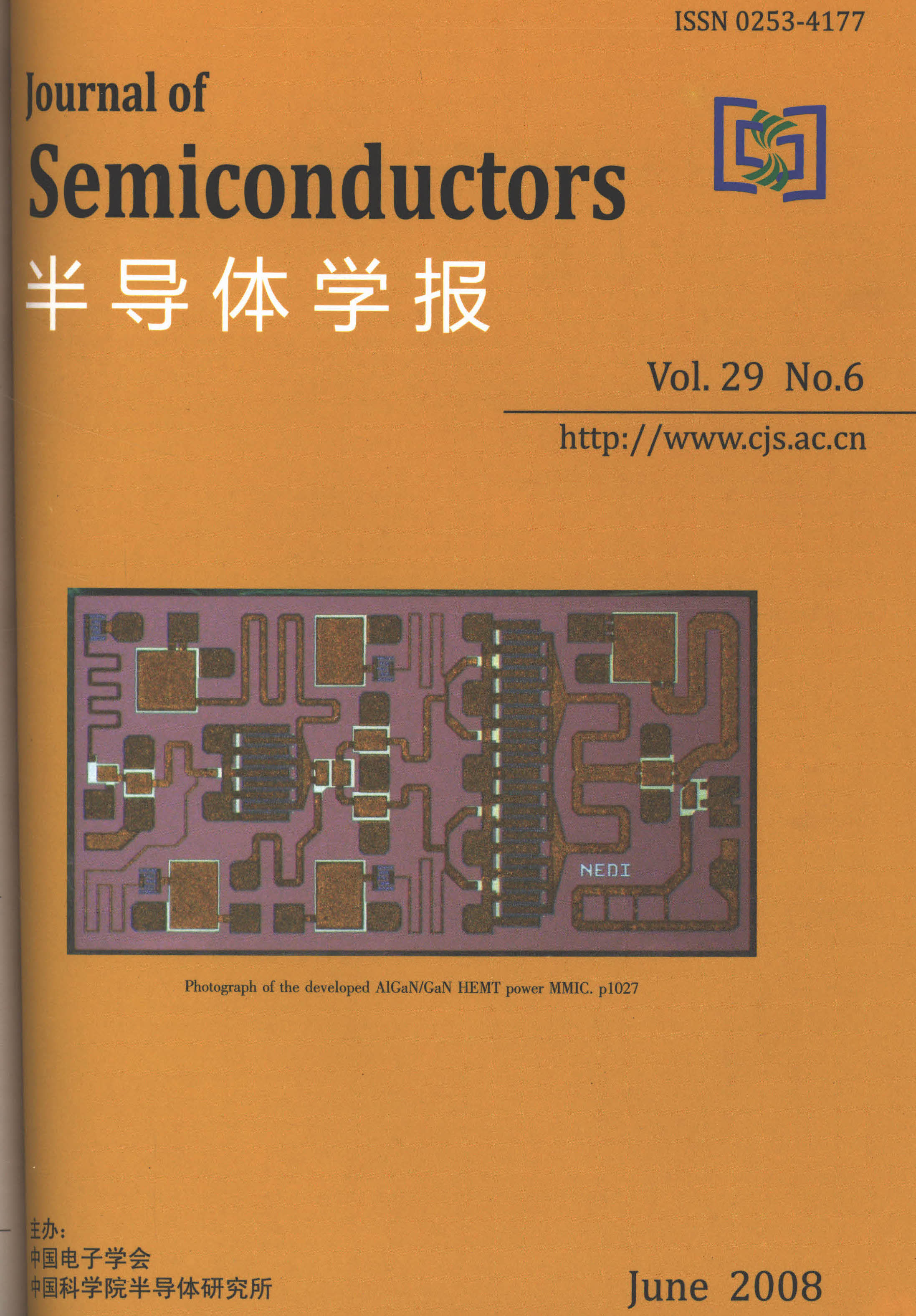
The development of an AlGaN/GaN HEMT power MMIC on SI-SiC designed in microstrip technology is presented.A recessed-gate and a field-plate are used in the device processing to improve the performance of the AlGaN/GaN HEMTs.S-parameter measurements show that the frequency performance of the AlGaN/GaN HEMTs depends significantly on the operating voltage.Higher operating voltage is a key to higher power gain for the AlGaN/GaN HEMTs.The developed 2-stage power MMIC delivers an output power of more than 10W with over 12dB power gain across the band of 9~11GHz at a drain bias of 30V.Peak output power inside the band reaches 14.7W with a power gain of 137dB and a PAE of 23%.The MMIC chip size is only 2.0mm×1.1mm.This work shows superiority over previously reported X-band AlGaN/GaN HEMT power MMICs in output power per millimeter gate width and output power per unit chip size.
We propose a novel all-optical sampling method using nonlinear polarization rotation in a semiconductor optical amplifier.A rate-equation model capable of describing the all-optical sampling mechanism is presented in this paper.Based on this model,we investigate the optimized operating parameters of the proposed system by simulating the output intensity of the probe light as functions of the input polarization angle,the phase induced by the polarization controller,and the orientation of the polarization beam splitter.The simulated results show that we can obtain a good linear slope and a large linear dynamic range,which is suitable for all-optical sampling.The operating power of the pump light can be less than 1mW.The presented all-optical sampling method can potentially operate at a sampling rate up to hundreds GS/s and needs low optical power.
The first domestic total dose hardened 2μm partially depleted silicon-on-insulator (PDSOI) CMOS 3-line to 8-line decoder fabricated in SIMOX is demonstrated.The radiation performance is characterized by transistor threshold voltage shifts,circuit static leakage currents,and I-V curves as a function of total dose up to 3E5rad(Si).The worst case threshold voltage shifts of the front channels are less than 20mV for nMOS transistors at 3E5rad(Si) and follow-up irradiation and less than 70mV for the pMOS transistors.Furthermore,no significant radiation induced leakage currents and functional degeneration are observed.
A multiplexer with a low-distortion high-bandwidth analog switch is presented.The gate-to-source voltage of the switch is set by the combined on-voltage of a pMOS and an nMOS,and the difference between its gate-source voltage and the threshold voltage (VGST) is guaranteed to be constant with input variation.Thus,the body effect is nearly canceled.Implemented in a TSMC 0.18μm CMOS process,results from HSPICE simulation show that the VGST is nearly constant with an input range from 0.3 to 1.7V,and the -3dB bandwidth is larger than 10GHz;the SFDR (spurious free dynamic range) of the output is 67.11dB with 1GHz input frequency;the turn-on time is 2.98ns,and the turn-off time is 1.35ns,which indicates a break-before-make action of the multiplexer.The proposed structure can be applied to high speed signal transmission.
Aiming at the specific protocol of RFID technology,a 915MHz CMOS transmitter front-end for OOK modulation is implemented in a 0.18μm CMOS process.The transmitter incorporates a class-E power amplifier (PA),a modulator,and a control logic unit.The direct-conversion architecture minimizes the required on-and-off-chip components and provides a low-cost and efficient solution.A novel structure is proposed to provide the modulation depth of 100% and 18%,respectively.The PA presents an output 1dB power of 17.6dBm while maintaining a maximum PAE of 35.4%.
Missing via has been a defect in semiconductor manufacturing,especially of foundries. Its solution can be rather attractive in yield improvement for relatively mature technology since each percentage point improvement will mean significant profit margin enhancement. However,the root cause for the missing via defect is not easy to determine since many factors,such as,defocus,material re-deposition,and inadequate development,can lead to missing via defects. Therefore,knowing the exact cause for each defect type is the key.In this paper,we will present the analysis methodology used in our company. In the experiments,we have observed three types of missing vias. The first type consists of large areas,usually circular,of missing patterns,which are primarily located near the wafer edge.The second type consists of isolated sites with single partially opened vias or completely unopened vias.The third type consists of relatively small circular areas,within which the entire via pattern is missing.We have first tried the optimization of the developing recipe and found that the first type of missing via can be largely removed through the tuning of the rinse process,which improves the cleaning efficiency of the developing residue. However,this method does not remove missing via of the second and third type. We found that the second type of missing via is related to local defocus caused by topographical distribution. To resolve the third type of missing via defects,we have performed extensive experiments with different types of developer nozzles and different types of photomasks,and the result is that we have not found any distinct dependence of the defect density on either the nozzle or the mask types. Moreover,we have also studied the defect density from three resists with different resolution capability and found a correlation between the defect density and the resist resolution. It seems that,in general,lower resolution resists also have lower defect density.The results will be presented in the paper.
Cu-excess CuxAlO2 ceramics with delafossite phases were synthesized using sol-gel.In the composition range of 1≤x<1.04,there are no detectable non-delafossite phases.Weak diffraction peaks of CuO are observed when x≥1.04.The room temperature conductivity of the Cu1.04AlO2 sample is improved by nearly an order of magnitude over that of the CuAlO2 sample.The major defect mechanism responsible for the conductivity enhancement is proposed to be substitution defects of CuAl (Cu2+ ions substitute Al3+ ions).The composition formula unit for Cu-excess CuxAlO2 may be expressed as Cu(Al1-yCuy)O.2.
Silicon crystal-facet-dependent nanostructures have been successfully fabricated on a (100)-oriented silicon-on-insulator wafer using electron-beam lithography and the silicon anisotropic wet etching technique.This technique takes advantage of the large difference in etching properties for different crystallographic planes in alkaline solution.The minimum size of the trapezoidal top for those Si nanostructures can be reduced to less than 10nm.Scanning electron microscopy (SEM) and atomic force microscopy (AFM) observations indicate that the etched nanostructures have controllable shapes and smooth surfaces.
A Schottky gate resonant tunneling transistor (SGRTT) is fabricated.Relying on simulation by ATLAS software,we find that the gate voltages can be used to control the current of SGRTT when the emitter terminal is grounded and a positive bias voltage is applied to the collector terminal.When the collector terminal is grounded,the gate voltages can control the peak voltage.As revealed by measurement results,the reason is that the gate voltages and the electric field distribution on emitter and collector terminal change the distribution of the depletion region.
Although outstanding microwave power performance of AlGaN/GaN HEMTs has been reported,drain current collapse is still a problem.In this paper,an experiment was carried out to demonstrate one factor causing the collapse.Two AlGaN/GaN samples were annealed under N2-atmosphere with and without carbon incorporation,and the XPS measurement technique was used to determine that the concentration of carbon impurity in the latter sample was far higher than in the former.From the comparison of two Id-Vds characteristics,we conclude that carbon impurity incorporation is responsible for the severe current collapse.The carbon impurity-induced deep traps under negative gate bias stress can capture the channel carriers,which release slowly from these traps under positive bias stress,thus causing the current collapse.
Asymmetric doping channel (AC) partially depleted (PD) silicon-on-insulator (SOI) devices are simulated using two-dimensional simulation software.The electrical characteristics such as the output characteristics and the breakdown voltage are studied in detail.Through simulations,it is found that the AC PD SOI device can suppress the floating effects and improve the breakdown characteristics over conventional partially depleted silicon-on-insulator devices.Also compared to the reported AC FD SOI device,the performance variation with device parameters is more predictable and operable in industrial applications.The AC FD SOI device has thinner silicon film,which causes parasitical effects such as coupling effects between the front gate and the back gate and hot electron degradation effects.
Temperature characteristics are important for the performance of organic thin film devices.On the basis of the hopping theory of Miller-Abrahams,an analytical model of charge transport for bilayer organic devices under the organic-organic interface limited current conduction is developed.The dependence of current,field,and carrier distribution in bilayer organic devices with the structure of "injection electrode/LayerI/LayerII/collection electrode" on temperature are numerically analyzed.We conclude that,for a given applied voltage,when temperature is raised,the voltage of LayerIwill increase,and the field will be higher.Meanwhile,the voltage of LayerIIwill decrease,the field will become weaker accordingly,and the current of the device will increase.
This paper presents the results of a numerical investigation of micro-sized particle removal by droplet impact.Computational fluid dynamics simulation is used to calculate the flow distribution of droplet impact on a flat surface.The hydrodynamic forces exerted on the particle are then computed.Key factors controlling particle removal are discussed.Both hydrophilic and hydrophobic surfaces are considered.The flow distributions,especially the front edge expanding upon impact at microscale,strongly depend on surface wettability.The associated hydrodynamic forces on the particles vary accordingly.In addition,the impact on a dry surface can produce higher removal efficiency than that on a wet surface.Under the same impact conditions,the drag force exerted on a particle residing on a dry surface can be three orders of magnitudes larger than on a wet surface.Improving droplet impact velocity is more effective than improving droplet size.
This paper experimentally studies the effects of the conductivity of a silicon wafer and the gap height between silicon structures and glass substrate on the footing effect for silicon on glass (SOG) structures in the deep reactive ion etching (DRIE) process.Experiments with gap heights of 5,20,and 50μm were carried out for performance comparison of the footing effect.Also,two kinds of silicon wafers with resistivity of 2~4 and 0.01~0.03Ω·cm were used for the exploration.The results show that structures with resistivity of 0.01~0.03Ω·cm have better topography than those with resistivity of 2~4Ω·cm;and structures with 50μm-high gaps between silicon structures and glass substrate suffer somewhat less of a footing effect than those with 20μm-high gaps,and much less than those with 5μm-high gaps.Our theoretical analysis indicates that either the higher conductivity of the silicon wafer or a larger gap height between silicon structures and glass substrate can suppress footing effects.The results can contribute to the choice of silicon type and optimum design for many microsensors.
HF etching of sacrificial layers with different structures,namely channel,bubble,and joint-channel,is studied.The existing model cannot fit the experimental data well.The error of etching rate between the existing model and the experimental data increases with etching time.A modified model considering the diffusion coefficient as a function of HF concentration and temperature is proposed.The etching rate coefficient as a function of temperature and the effect of reaction production are also considered in the modified model.For the joint-channel structure,a new mathematical model for the etching profile is also adopted.Experimental data obtained with channel,bubble,and joint-channel structures are compared with the modified model and the previous model.The results show that the modified model matches the experiments well.
The monolithic integrated micro sensor is an important direction in the fields of integrated circuits and micro sensors.In this paper,a monolithic themral vacuum sensor based on a micro-hotplate (MHP) and operating under constant bias voltage conditions was designed.A new monolithic integrating mode was proposed,in which the dielectric and passivation layers in standard CMOS processes were used as sensor structure layers,gate polysilicon as the sacrificial layer,and the second polysilicon layer as the sensor heating resistor.Then, the fabricating processes were designed and the monolithic thermal vacuum sensor was fabricated with a 0.6μm mixed signal CMOS process followed by sacrificial layer etching technology.The measurement results show that the fabricated monolithic vacuum sensor can measure the pressure range of 2~1E5Pa and the output voltage is adjustable.
The transient resistance,voltage,and power of a nonlinear GaAs photoconductive semiconductor switch (PCSS) are presented by the finite difference formula to deal with the experiment data,based on the conversation of energy in the switch circuit.This method resolves the problem of directly measuring the transient characteristics of PCSS in nonlinear mode.The curve of transient voltage shows that the average electric field of PCSS in the lock-on period is always higher than the Gunn threshold,and increases monotonically.By comparing the transient power curves of the PCSS and the electrical source,it is demonstrated directly that the power shortage leads to the PCSS from the lock-on state into the self-turnoff state,so a controllable turnoff of the PCSS in lock-on by changing the distribution of the circuit power is predicted.
This paper introduces a new technology to fabricate a micro electromagnetic actuator with high energy density without an enclosed magnetic circuit.This technology includes fabricating multi-turns planar micro coils and fabricating the thick magnetic (NiFe) core on the silicon wafer.The multi-turns planar micro coils are fabricated by the electroplating method from the surface along the line and by dynamically controlling the current density of the copper electrolytes.In order to fabricate thick NiFe plating,the adhesion properties between the NiFe plating and the silicon substrates are improved by changing the surface roughness of the silicon substrates and increasing the thickness of the seed layer.Furthermore,the micro electromagnetic actuator is tested and the energy density of the actuator is evaluated by force testing.The experiments show that the microactuator is efficient in producing high magnetic energy density and high magnetic force.
A DC-10Mb/s laser diode driver,compatible with TTL and CMOS levels,is presented.The optical power corresponding to ‘1’ and ‘0’ can be set independently with resistors off-chip and stabilized with a closed loop.A novel peak-to-peak optical power monitor and stabilization mechanism is introduced.The circuit,fabricated in a CSMC 0.5μm mixed signal CMOS process,can provide 120mA maximum drive current and 0.6dB extinction ration fluctuation over -20~+80℃,which is independent of input pattern.
A novel charge exchanging compensation (CEC) technique is proposed for a wideband sample-and-hold (S/H) circuit applied in an IF sampling ADC.The CEC technique compensates the sampling bandwidth by eliminating the impact from finite on-resistance of the sampling switch,and avoids increasing clock feedthrough and charge injection.Meanwhile,a low power two stage OTA with a class AB output stage is designed to provide the S/H a 3Vp-p input range under 1.8V power.The S/H achieves a 94dB spurious-free dynamic range for a 200MHz input signal at a 100Ms/s sample rate and consumes only 26mW with a 5.5pF load.
A quadrature mixer with a shared transconductor stage is analyzed,including voltage conversion gain,linearity,noise figure,and image rejection.The analysis indicates it has better performance than a conventional Gilbert mixer pair in commutating mode.A quadrature down-conversion mixer based on this topology is designed and optimized for an ultra high frequency RFID reader.Operating in the 915MHz ISM band,the presented quadrature mixer measures a conversion gain of 12.5dB,an IIP3 of 10dBm,an IIP2 of 58dBm,and an SSB noise figure of 17.6dB.The chip was fabricated in a 0.18μm 1P6M RF CMOS process and consumes only 3mA of current from a 1.8V power supply.
Texture and grain boundary character distribution of Cu interconnects with different line width for as-deposited and annealed conditions were measured by EBSD.All specimens appear mixed texture and (111) texture is the dominate component.As-deposited interconnects undergo the phenomenon of self-annealing at RT,in which some abnormally large grains are found.Lower aspect ratio of lines and anneal treatment procured larger grains and stronger (111) texture.Meanwhile,the intensity proportion of other textures with lower strain energy to (111) texture is decreased.As-deposited specimens reveal (111)〈112〉 and (111)〈231〉 components.(111)〈110〉 component appeared and (111)〈112〉 and (111)〈231〉 components were developed during the annealing process.High angle boundaries are dominant in all specimens,boundaries with a misorientation of 55°~60° and Σ3 ones in higher proportion,followed by lower boundaries with a misorientation of 35°~40° and Σ9 boundaries.As the aspect ratio of lines and anneal treatment increase,there is a gradual increment in Σ3 boundaries and a decrease in Σ9 boundaries.
The electronic structure and optical properties of impurity (Mn,Cr,Co,Ni)-doped β-FeSi2 have been studied using the first principle plane-wave pseudo-potential based on the density function theory.The calculated results show that Mn prefers the FeI site,whereas Cr,Co,and Ni prefer the FeII site.The change about the volume and the atom position of the β-FeSi2 cell depends strongly on the species of dopants and the doped atom’s sites.The Fermi surface moves to the valence band with impurity from Mn or Cr and the β-FeSi2 becomes a p-type semiconductor while the Fermi surface moves to the conduction band with impurity from Co or Ni and the β-FeSi2 becomes a n-type semiconductor.The dopants can provide large numbers of carriers near the Fermi energy and change the properties of the interband transition of electrons.
The paper elaborates on the characteristics of the transmission coefficient and the shot noise of a ferromagnetic/semiconductor/ferromagnetic heterojunction with double δ tunnel barrier in the existing external magnetic field.The effects of the quantum size and Rashba spin-orbit coupling are discussed.The results show that the transmission coefficient and the shot noise continuously oscillate as the length of the semi-conductor changes when the spin-dependent electron tunnels through the hetero-junction.The frequency of the transmission coefficient and the shot noise increase as the Rashba spin-orbit coupling and the external magnetic increase.The frequency of the shot noise will change as the angle of the external magnetic changes.The existence of the double δ tunnel barrier increases the swing of the transmission coefficient of the spin-electron
Diamond films were prepared by an electron assisted chemical vapor deposition system (EA-CVD) in an atmosphere with a nitrogen addition.SEM,Raman spectroscopy,and EPR were employed to study the influence of nitrogen on the films’ quality and the characteristics of nitrogen doping.The results show that for the films deposited at 950℃,the morphology changes to cauliflower-like structures,the content of non-diamond carbon increases,and the quality drops after adding nitrogen into the atmosphere.For the films deposited at 800℃,the addition of nitrogen reduces the twins and secondary nucleation,and improves the films' morphology.EPR and Raman spectra indicate that nitrogen impurities in the films mainly exist in the forms of Ns0,[N-V]0,and [N-V]-1.Along with the increase of nitrogen flow rate,the content of Ns0 increases,the content of [N-V]0 decreases,and the content of [N-V]-1 does not change obviously.
High-pressure and high-temperature are used to treat a series of Co doped ZnO samples synthesized by Sol-gel method.Structure and composition analyses suggest that CoO is formed after increasing the Co concentration under the high-pressure condition.The results of magnetism measurements by SQUID show that all the samples have room-temperature ferromagnetism and the ferromagnetism increases as the Co doping concentration increases,despite the formation of antiferromagnetic CoO under the high pressure condition.Thus,we argue that the ferromagnetism of ZnCoO is intrinsic.
μc-Si:H films were deposited under different power density by VHF-PECVD.The microstructure of the films was investigated.The effect of power density on the deposition rate and crystallization of μc-Si:H was studied extensively.This study shows that as the power density increased,the deposition rate first increased gradually and then saturated.The thickness of the incubation layer and the nucleation density varied with power density.
Based on the growth requirement in MOCVD processes,the five optimum transport conditions are summarized as:uniform concentration boundary layer,uniform velocity boundary layer,uniform temperature boundary layer,reactants mixed uniformly before entering the reaction zone,and the exhaust gas expelled quickly without remixing with the reactants.Compared with the optimum conditions,the current MOCVD reactors of horizontal,vertical,planetary,showerhead,and RDR types are discussed.The main problems in horizontal reactors are reactant depletion,thermal convection,and reactor side effects.Using injection from showerheads and high speed susceptor rotation,the vertical reactors can obtain much more uniform boundary layers.The main problems in vertical reactors are the difficulty in expelling the exhaust gas without remixing with reactants and the difficulty in further enlarging the diameter of the rotating susceptor.
Boron-doped solution-based metal induced crystallized poly-Si thin film has good electrical characteristics and optical characteristics with semi-transparent and semi-reflective functions.It can be used as an LCD electrode that is both transparent and reflective.However,the transmission and reflection character of the MIC poly-Si thin film is different among the red,green,and blue (R,G,B) color regions,resulting in the "aberrance" of the composing white light.Accordingly,high reflectivity Al with different area was etched and adopted to compensate and balance the three essential color light permeating and reflecting from the MIC p-Si electrode when TFT source and drain metal Al electrodes were being prepared.The experimental results indicate that in the range of visible light,the reflectivity and transmissivity of red,green,and blue light basically meet the requirement of white light balance.Consequently,using this technique,an LCD panel that has both transparent and reflective functions has been obtained.
An InGaAsP waveguide is integrated laterally to MQW using LP-MOCVD butt-joint technology. High quality for the regrowth interface and material is achieved.The loss of the butt-jointed waveguide is 7cm-1.This demonstrates the applicability of butt-joint technology in fabricating high quality future photonic integrated circuits.
This paper first establishes a 3D molecular dynamics simulation model for abrasive wear.The Einstein model in solid-state physics is introduced for the conversion between the kinetic energy and temperature of the diamond atom.Then,a 3D MD program is made and executed.The results that the abrasion occurs in the early of period of the grinding.With the advance of the grinding,this kind of wear is no longer seen and the grinding comes into a steady state.In addition,the abrasive wear only can be found in the bottom of the abrasive and the surface effect has a close relation with the abrasion.The surface effect causes the shortage of configuration of atoms in the bottom of the abrasive.Thus,there are defects on the surface of the abrasive,especially at the bottom of the abrasive where the atoms have strong activity and are in an unstable condition.According to the least-energy principle,these atoms will release the energy spontaneously through plastic deformation and amorphous phase transformation,producing the wear.
The optical properties of several typical III-nitride semiconductors were investigated by cathodoluminescence (CL) unitized systems.The CL unitized systems are combined with a thermal field-emission scanning electron microscopy (JEOL JSM-7000F) and a high performance CL spectroscopy (Gatan Mono CL3) equipped LN-cooling stage.Two aspects can be obtained from the measurements: (1) CL spectrum.Using a UV-visible CL spectrum system,the optical properties of unintentionally-doped and Mg-doped AlxGa1-xN films grown on c-plane sapphire are analyzed.This analysis indicates that the peak intensity of near band edge emission at 4.6eV increases proportionally with excitation power density.However,that the intensity of the 3.9eV band originated from a Mg-doped impurity-level shows saturation independence with excitation power density.Furthermore,the CL from InN films is measured with a near infrared (NIR) CL system,which proves that the optical band gap of InN locates at 0.77eV. (2) CL mapping.The CL unitized systems can give the luminescence area at different wavelength in the UV-visible range.The free-standing GaN substrates grown by hydride vapor phase epitaxy are analyzed combining SEM and CL mapping methods.The edge type dislocations are observed under the surface using CL mapping instead of SEM.The type,distribution,and luminescence properties of dislocations are studied.
The photosensitive Pb0.91La0.09(Zr0.65Ti0.35)O.3 (PLZT) precursor sols are prepared by a modified sol-gel process with benzoylacetone as chemical modification to form a coordination chelate structure of metal-salt with PVP as an addition agent for suppressing film cracks.The patterns of PLZT gel films are prepared by direct patterning process and single dip-coating,and the PLZT film patterns with perovskite structure on Pt/TiO2/SiO2/Si substrate are obtained after heat-treatment.The PLZT film’s pattern thickness is about 260nm,of which the remnant polarization,coercive field,and fatigue behavior are about 6.7μC/cm2,77kV/cm,and 1E7 respectively.The dielectric loss and dielectric constant are 0.02 and 356 at 10kHz,respectively.
Selective dry etching of GaAs/AlAs with SiCl4/SF6 mixtures by inductively coupled plasma (ICP) is reported.With different SiCl4/SF6 ratios,chamber pressure,and RF chuck power,the average etch rates of GaAs,AlAs,and their selectivity are studied.Proper gases ratios of SiCl4/SF6(15/5sccm),lower RF chuck power,and higher chamber pressure enhance the formation of AlF3 nonviolent produce and encourage to the selectivity of GaAs/AlAs.When the gases ratios of SiCl4/SF6 are at 15/5sccm,RF chuck power is 10W,source power is 500W,and chamber pressure is 2Pa,the selectivity of GaAs/AlAs reaches at least 1500.The plasma damage of etched GaAs substrate is conducted by Raman spectroscope under different RF chuck power and chamber pressure,atomic force microscope (AFM),and scanning electron microscope (SEM) also have been applied to view the surface morphology and sidewall,respectively.
A novel control structure for a DC-DC converter is presented.At light loads,the chip enters power save mode automatically and works in fixed peak current mode with standby intervals by detecting the feedback voltage.It reduces the average quiescent and switching power loss greatly,which increases efficiency at light loads and extends battery life in portable systems.Internal synchronous rectification eliminates the need for a Schottky diode and increases efficiency further.A DC-DC buck converter with the proposed structure has been fabricated with a 0.5μm CMOS process for validation.Under the condition of 3.6V input and 1.8V output,the quiescent current in the standby state is only 25μA.The measured efficiency for a 0.1mA load current is up to 62% and the maximum efficiency is 96%.
An RF front-end circuit for a fully integrated CMOS DTV tuner is presented in this paper,where double-conversion low IF architecture is employed.The chip is implemented in a 0.18μm CMOS process,which includes a wideband low noise amplifier,and upconversion and downconversion mixers.The measurement results show the front-end has good input matching and a 20dB variable gain range.In the maximum gain mode,the gain is +33dB,the single sideband noise figure (SSB NF) is 9.6dB,and the input referred third-order intercept point (IIP3) is -6dBm;In the minimum gain mode,the gain is +14dB,the SSB NF is 28dB,and the IIP3 is +8dBm.The RF front-end drains 30mA current from a 1.8V supply and the die area is about 1.04mm×0.98mm.
A soft-start circuit based on DAC (digital-to-analog converter) control for DC-DC switching regulator is presented.Using the techniques of DAC control and soft-start voltage sense,the rush current and overshoot of the output voltage during start-up are eliminated effectively,allowing for a smooth output voltage ramp from zero to regulation.At the end of start-up,the biased current of the soft-start circuit is cut off completely. Consequently,it is power-efficient.The circuit is designed using CMOS devices without the need of any external components,so it is suitable for integration in DC-DC switching regulators.The proposed soft-start circuit has been applied to a Buck PWM controller successfully.The experimental results show that in the entire load range the output of the system can start up smoothly,the inductor current remains stable,the output voltage rises smoothly without overshot,and the soft-start time is about 1.2ms.
A band III PLL Frequency Synthesizer is integrated in a 0.18μm 1.8V CMOS process,except for the tuned inductor and loop filter.Some functions such as selecting the sub-band of the VCO,configuring the currents of the charge pump and VCO etc,can be performed by using the SPI bus.An improved band-switching circuit is adopted to save band-switching time.As the measurement results show,the total power of the frequency synthesizer is 34mW;the frequency range of frequency synthesizer’s output is 143~271Mhz.The phase noise in band III can reach -83dBc/Hz@10kHz,-104dBc/Hz@100kHz and the reference spur is less than -70dBc.This new band-switching circuit can save band-switching time in comparison with the normal one.