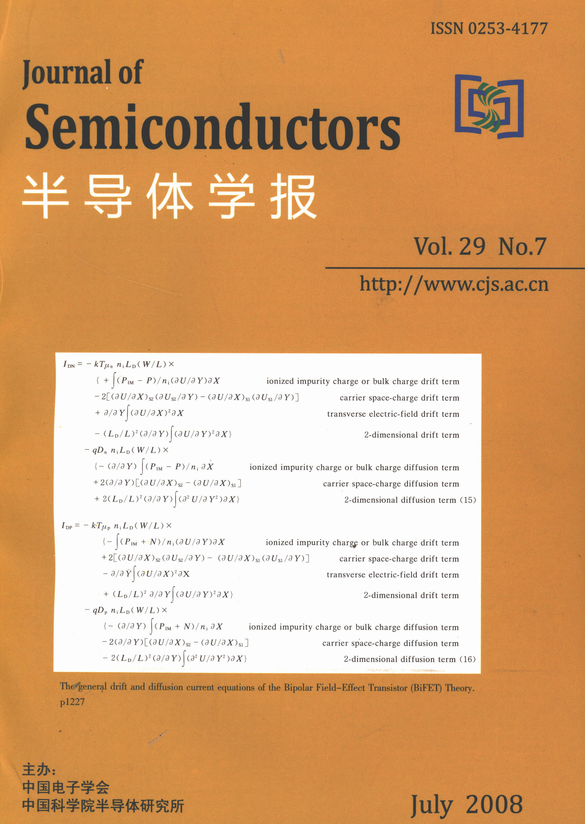
The previous report (XI) gave the electrochemical-potential theory of the Bipolar Field-Effect Transistors.This report (XII) gives the drift-diffusion theory.Both treat 1-gate and 2-gate,pure-base and impure-base,and thin and thick base.Both utilize the surface and bulk potentials as the parametric variables to couple the voltage and current equations.In the present drift-diffusion theory,the very many current terms are identified by their mobility multiplier for the components of drift current,and the diffusivity multiplier for the components of the diffusion current.Complete analytical drift-diffusion equations are presented to give the DC current-voltage characteristics of four common MOS transistor structures.The drift current consists of four terms:1-D (One-Dimensional) bulk charge drift term,1-D carrier space-charge drift term,1-D E2X(transverse electric field) drift term,2-D drift term.The diffusion current consists of three terms:1-D bulk charge diffusion term,1-D carrier space-charge diffusion term,and 2-D diffusion term.The 1-D E2X drift term was missed by all the existing transistor theories,and contributes significantly,as much as 25% of the total current when the base layer is nearly pure.The 2-D terms come from longitudinal gradient of the longitudinal electric field,which scales as the square of the Debye to Channel length ratio, at 25nm channel length with nearly pure base,(LD/L)2=1E6,but with impurity concentration of 1E18cm-3,(LD/L)2=1E-2.
High-resolution X-ray diffraction has been employed to investigate the diffuse scattering in a (0001) oriented GaN epitaxial film grown on sapphire substrate.The analysis reveals that defect clusters are present in GaN films and their concentration increases as the density of threading dislocations increases.Meanwhile,the mean radius of these defect clusters shows a reverse tendency.This result is explained by the effect of clusters preferentially forming around dislocations,which act as effective sinks for the segregation of point defects.The electric mobility is found to decrease as the cluster concentration increases.
Tantalum nitride (TaN) and nichrome (NiCr) are the two most common materials used as thin film resistors (TFR) for monolithic microwave integrated circuits (MMIC) based on AlGaN/GaN high electron mobility transistors (HEMTs).In this study,we compare the reliability of the two materials used as TFRs on a semi-insulation 4H SiC substrate.Through the comparison between NiCr and TaN thin-film resistor materials,we find the square resistor (Rs) of TaN TFR increases as the annealing temperature increases.However,the Rs of NiCr TFR shows the opposite trend.We also find the change of the TaN Rs and contacted resistor (RC) is smaller than the NiCr.After O.2 plasma exposure in RIE,the TaN Rs only decreases 0.7Ω,or about 2.56%,and RC increases 0.1Ω,or about 6.6%,at an annealing temperature of 400℃.In contrast,the NiCr Rs and RC show large changes at different annealing temperatures after O.2 plasma exposure.In conclusion,TaN is more stable during plasma exposure after 400℃ annealing in N2 ambient.
A novel CMOS bandgap reference is presented.The output reference of this new current mode structure can be set to an arbitrary value above the bandgap voltage of silicon,avoiding offset in application.It also overcomes the systematic mismatch of conventional current mode bandgap references.The proposed bandgap reference has been implemented in UMC 0.18μm mixed mode technology.Under the supply voltage of 1.6V,the proposed bandgap reference provides an output reference of 1.45V and consumes 27μA of supply current.Using no curvature compensation,it can reach a temperature coefficient of 23ppm/℃ from 30 to 150℃ with a line regulation of 2.1mV/V from 1.6 to 3V and a PSRR of 40dB at DC frequency.The chip area of the bandgap reference (without pad) is 0.088mm2.
Heteroepitaxial growth of 3C-SiC on patterned Si substrates by low pressure chemical vapor deposition (LPCVD) has been investigated to improve the crystal quality of 3C-SiC films.Si substrates were patterned with parallel lines,1 to 10μm wide and spaced 1 to 10μm apart,which was carried out by photolithography and reactive ion etching.Growth behavior on the patterned substrates was systematically studied by scanning electron microscopy (SEM).An air-gap structure and a spherical shape were formed on the patterned Si substrates with different dimensions.The air gap formed after coalescence reduced the stress in the 3C-SiC films,solving the wafer warp and making it possible to grow thicker films.XRD patterns indicated that the films grown on the maskless patterned Si substrates were mainly composed of crystal planes with (111) orientation.
Lattice matched Ga1-xInxAsySb1-y quaternary alloy films for thermophotovoltaic cells were successfully grown on n-type GaSb substrates by liquid phase epitaxy.Mirror-like surfaces for the epitaxial layers were achieved and evaluated by atomic force microscopy.The composition of the Ga1-xInxAsySb1-y layer was characterized by energy dispersive X-ray analysis with the result that x=0.2,y=0.17.The absorption edges of the Ga1-xInxAsySb1-y films were determined to be 2.256μm at room temperature by Fourier transform infrared transmission spectrum analysis,corresponding to an energy gap of 0.55eV.Hall measurements show that the highest obtained electron mobility in the undoped p-type samples is 512cm2/(V·s) and the carrier density is 6.1E16 cm-3 at room temperature.Finally,GaInAsSb based thermophotovoltaic cells in different structures with quantum efficiency values of around 60% were fabricated and the spectrum response characteristics of the cells are discussed.
The 1/fγ noise characteristic parameterSfγ model in an n-MOSFET under DC hot carrier stress is studied.A method characterizing the MOSFET abilities of an anti-hot carrier with noise parameter Sfγ is presented.The hot carrier degradation effect of n-MOSFET in high-,mid-,and low gate stresses and its 1/fγ noise feature are studied.Experimental results agree well with the developed model.
There is growing interest in developing high-voltage MOSFET devices that can be integrated with low-voltage CMOS digital and analog circuits.In this paper,high-voltage n- and p-type MOSFETs are fabricated in a commercial 3.3/5V 0.5μm n-well CMOS process without adding any process steps using n-well and p-channel stops.High current and high-voltage transistors with breakdown voltages between 23 and 35V for the nMOS transistors with different layout parameters and 19V for the pMOS transistors are achieved.This paper also presents the insulation technology and characterization results for these high-voltage devices.
We solve the single mode coupled rate equations by computer,simulate the behavior of a gain switch of an AlGaInP red light semiconductor laser diode,and find the characteristic of FWHM of pulses changing with the amplitude of modulation signal,the bias current,and the modulated frequency.On this basis,we conduct experiments.The experiment results accord with the simulations well.
An InP-based one-dimensional photonic crystal quantum cascade laser is realized.With photo lithography instead of electron beam lithography and using inductively coupled plasma etching,four-period air-semiconductor couples are defined as Bragg reflectors at one end of the resonator.The spectral measurement at 80K shows the quasi-continuous-wave operation with the wavelength of 5.36μm for a 22μm-wide and 2mm-long epilayer-up bonded device.
A resistivity distribution with a space of 3mm between test points was measured on a slice-of-silicon monocrystal (diameter 75mm) using an inclined four-point probe.This paper has determined the number of resistivity divisions and their separations by statistical methods and introduced fuzzy mathematics to place the data into different fuzzy sets,after choosing the exponent function as a membership function for fuzzy sets and suitable values of thresholds.One fuzzy set corresponds to one resistivity isocontour.Then,the resistivity isocontours can be drawn with a definite separation and finally shown in a map with MATLAB.The deviation of resistivity data on an isocontour is small and there are few residual test points without connections.So,the connection of the isocontours are high-quality and useful in application for instructing practical production.
Through different dose-rate switching evaluation methods,the radiation-response rules of operational amplifiers are studied when the irradiation dose rate is switched from high to low under different radiation temperatures and total doses.The experimental results indicate that the response characteristics could be affected by the switching total doses,irradiation temperatures,and dose rates individually or together.Accelerated evaluation on the ELDRS can be realized by adopting a proper dose-rate switching method.Meanwhile,the irradiation time can also be reduced.Finally,the mechanisms of the difference between various radiation responses are analyzed.
A novel edge-triggered D-flip-flop based on a resonant tunneling diode (RTD) is proposed and used to construct a binary frequency divider.The design is discussed in detail and the performance of the circuit is verified using SPICE.Relying on the nonlinear characteristics of RTD,we reduced the number of components used in our DFF circuit to only half of that required using conventional CMOS SCFL technology.
A fractional-Nfrequency synthesizer for 433/868MHz SRD applications is implemented in a 0.35μm CMOS process.A wide-band VCO and an AFC are used to cover the desired bands.A 3bit third order sigma-delta modulator is adopted to reduce the out-band phase noise.The measurements show a VCO tuning range from 1.31 to 1.88GHz with AFC working correctly,an out-band phase noise of -139dBc/Hz at 3MHz offset frequency,and a fractional spur of less than -60dBc.The chip area is 1.5mm×1.2mm and the total current dissipation including LO buffers is 19mA from a single 3.0V supply voltage.
To meet the demands for different supply voltage levels on SOC required by digital modules like CPU core and analog modules,a novel dual-output charge pump is proposed.The charge pump can output a step-up and a step-down voltage simultaneously with a high driving capability.The multiple gain pair technique was introduced to enhance its efficiency.The proposed co-use technology for capacitors and switch arrays reduced its cost.The charge pump was designed and fabricated in a TSMC 0.35μm mixed-signal CMOS process.A group of analytical equations were derived to model its static characteristics.A state-space model was derived to describe its small-signal dynamic behavior.Analytical predictions were verified by Spectre simulation and testing.The consistency of simulated results as well as test results with analytical predictions demonstrated the high precision of the derived analytical equations and the developed models.
For performance optimization such as placement,interconnect synthesis,and routing,an efficient and accurate interconnect delay metric is critical,even in design tools development like design for yield (DFY) and design for manufacture (DFM).In the nanometer regime,the recently proposed delay models for RLC interconnects based on statistical probability density function (PDF) interpretation such as PRIMO,H-gamma,WED and RLD bridge the gap between accuracy and efficiency.However,these models always require table look-up when operating.In this paper,a novel delay model based on the Birnbaum-Saunders distribution (BSD) is presented.BSD can accomplish interconnect delay estimation fast and accurately without table look-up operations.Furthermore,it only needs the first two moments to match.Experimental results in 90nm technology show that BSD is robust,easy to implement,efficient,and accurate.
The influences of lattice vibration and polaron effects on the ground state and the excited state of the system,for which the exciton is strongly coupled with interface-optical (IO) phonons but weakly or intermediately coupled with bulk-longitudinal-optical (LO) phonons in a quantum well,are studied using the linear-combination operator and the LLP variational method.The expressions for the ground state energy shift and the first internal excited state energy shift of the exciton as a function of the well width and temperature are derived.Numerical calculations for an AgCl/AgBr/AgCl QW,for example,are performed.The results indicate that the ground state energy shift and the first internal excited state energy shift increases with the temperature for strong exciton-IO-phonon coupling but decreases with the temperature for weak exciton-LO-phonon coupling.
The generation,relaxation,and recombination of hot carriers in ZnSeTe/ZnTe type II multiple quantum well (MQW) structures are investigated using photoluminescence (PL) spectra and the femtosecond pulse pump-probe technique.The generation of hot carriers in barrier layers and well layers is observed by time-resolved differential transmission spectra.The cooling time of hot carriers in ZnTe layers is about 10ps.Carrier capturing from the ZnTe barrier layer to the ZnSeTe well layer is also in the time scale of 10ps.
Nitrogen-doped ZnO (ZnO:N) films are prepared by thermal oxidation of sputtered Zn3N2 layers on Al2O3 substrate.The dependence of the structural and optical properties of the ZnO:N films on annealing temperature is investigated.X-ray Diffraction (XRD) results illustrate that the as-sputtered Zn3N2 films can be transformed into ZnO:N films after annealing at 600℃ and above.X-ray photoelectron spectroscopy (XPS) reveals that nitrogen has two chemical states in the ZnO:N films:(N2)o and No,which denote substitution of molecular N for O and atomic N for O,respectively.Hall effect measurements illustrate that the hole concentration in ZnO:N films annealed at 700℃ is the highest.The FA and DAP transition peaks are observed in low temperature photoluminescence spectra,from which the nitrogen acceptor binding energy can be obtained.
High quality ZnO film of about 10μm thick has been successfully grown on a ZnAl2O4 buffer layer via metal vapor phase epitaxy (MVPE).The ZnAl2O4 buffer layer was prepared by high temperature annealing ZnO thin film grown by the sol-gel method.Double crystal x-ray diffraction (DCXRD) analysis indicates that unwanted orientations in the film are eliminated using the buffer layer and that the full width at half maximum (FWHM) of the (0002) rocking curve dramatically drops from 1371" to 342" .To our knowledge,this is the first report that a ZnAl2O4 buffer layer can enhance the quality of ZnO film grown by metal vapor phase epitaxy.
A MgZnO/ZnO p-n heterojunction was grown on GaAs substrate by metal-organic chemical vapor deposition.The I-Vcharacteristics showed a diode characteristic between the n-ZnO and p-MgZnO layers with a threshold voltage of 3.6V.When the injection current attained 50 mA,the emission was visible to the naked eye in the dark.Room temperature measurements,such as the HALL,XRD,PL,and EL spectra were carried out.The PL spectra of the n-ZnO and p-MgZnO layers both showed strong NBE peaks and weak broad DLE peaks.The EL spectra of the junction under different injection current all showed strong broad DLE peaks from 450 to 550nm,attributed to the deep-level transition.
The HgCdTe epilayers reported here were double-layers compositional heterojunctions grown by Te-rich liquid phase epitaxy in a horizontal slider system.The substrates adopted were (111) oriented CdZnTe with about 4% Zn.The epilayers were evaluated by the chemical staining method and infrared transmission spectra measurements.A phenomenological model was also established to characterize the profile of the Cd composition along the growth direction in the HgCdTe epilayer.The results of the electrical measurements showed that the carrier mobility of the long-wave layer beneath the double-layer sample was slightly higher than that of the single-layer sample grown with almost the same conditions.The reason for the increase of the mobility can be ascribed to the passive effect of the middle-wave cap layer.
4H-SiC films were grown on 75mm Si-face n-type substrates 4° off-oriented towards the 〈1120〉 direction using a horizontal hot-wall CVD system.Optical and atomic force microscopy results revealed the main defects observed were typical 4° off-large carrots,triangles,and a few down-falls.The most observable feature was the step bunching.By optimizing the process conditions,a low sigma/mean(σ/mean) value of 4.37% and 1.81% in doping concentration and thickness uniformity were obtained on the epitaxy films,respectively.
On the basis of combining the advantages of low dose separation by implanted oxygen (SIMOX) technology and bonding technology,a new technology named SIMOX wafer bonding (SWB) for fabricating a thin film(thin top silicon layer)/thick buried oxide (BOX) SOI was investigated.A thin film/thick BOX SOI with SOI layer thickness of 130nm,BOX thickness of 1μm,and SOI layer thickness uniformity of ±2% was fabricated with SWB technology.The surface morphology and structure of the thin film/thick BOX SOI were characterized using cross-sectional transmission electron microscopy (XTEM) and atomic force microscopy (AFM),respectively.The results suggest that the SOI layer of SWB can maintain the thickness uniformity of SIMOX and SWB SOI have an atomic scale SOI layer/BOX interface.Therefore,SWB is a promising technology for fabricating SOI material.
AlGaN/GaN HEMTs at the X band based on homemade SiC substrates and homemade epi-layers are first reported.A 0.35μm gate length,1mm gate width microwave power device is produced with a gate-connected field plate.The power device exhibits a maximum drain current density as high as 0.83A/mm and a peak extrinsic transconductance of 236mS/mm.A unity current gain cutoff frequency(fT) of 30GHz and a power gain cutoff frequency of 31GHz are obtained.The device biased at a drain voltage of 40V demonstrates a continuous wave saturated output power of 8W with a gain of 4.9dB and a power-added efficiency of 45% at 8GHz.
When a high-electron mobility transistor (HEMT) is driven by a terahertz (THz) field and magnetic field,plasma oscillation appears in the channel of the HEMT.We have investigated the effect of the THz field and magnetic field on the current characteristics of the HEMTs.The results show that the peaks of the responsivities of the HEMT exhibit blueshift as the magnetic field increases.We may tune the frequencies of the plasma oscillation by changing the magnetic field.
Based on metal-oxide-semiconductor field effect transistor (MOSFET) noise theory of carrier number fluctuation and mobility fluctuation,a forecast model of radiation-resistant capability is established.This model can preferably forecast post-irradiation threshold voltage drift due to oxide traps and interface traps through the pre-irradiation 1/f noise parameter.The simulation results of the model agree well with the measurement results.The forecast model is validated.The model provides a forecast technique for radiation-resistant capability on MOSFETs for engineering applications.
This paper will discuss the influence of the surface texture on the optical properties of LEDs by using the Monte Carlo method to simulate two dimensional red LEDs.The surface texture,which has a 4μm etching depth,2μm etching width,40 degree obliquity,and 2μm cycle,is formed by chemical etching.The experimental result indicates that the light-intensity increased by 20.56%.After analyzing the result of this simulation and experiment,we conclude that this method of introducing the surface texture has an effective impact on the light-intensity of LEDs
Wafer direct bonding technology has extensive application and broad prospects.UV activation combined with wet chemical cleaning in wafer direct bonding is investigated.An IR detection system,single tensile machine,and FSEM are employed to evaluate the bonding quality.The constant temperature and humility experiment,and the high and low temperature cycle experiment are also performed.It has been demonstrated that this approach can realize wafer direct bonding and enhance the bonding strength.A higher strength can be obtained by controlling the UV exposure time.The bonded wafer treated by constant temperature and humility and high and low temperature cycle can retain a higher bonding strength.Therefore,the process is effective for the wafer direct bonding and has great potential for application.
A wideband low noise amplifier (LNA) MMIC was designed and fabricated with 0.15μm GaAs pHEMT process.It obtains high gain by means of adopting four stages topology.The chip size is 2mm×1mm.Covering 45~65GHz,it achieves a maximum 20.5dB gain and low VSWR.It has the advantages of higher gain,wider bandwidth and lower power consuming.This chip can be widely applied in 60GHz wideband wireless communication system.
A grating moving light modulator (GMLM) modulates light energy by changing the distance of the movable grating and the underlying fixed reflector.The dielectric material SiO2 provides trap sites for charges both in the volume and the surface in high electric field,which will affect GMLM driving characteristic.With Gauss theory,the electrodynamic model is set up.The distribution of trapped charges and the relationship between the displacement of movable grating and applied voltage are analyzed in detail An experimental scheme is designed.The experiment indicates that increasing the applied voltage achieves the same displacement due to the influence of trapped charges,a longer charge time,and a bigger offset voltage,which is consistent with theoretical analysis.
Two types of variable-area photovoltaic detectors passivated by single ZnS layer and dual (CdTe/ZnS) layers have been fabricated on the same HgCdTe wafer.Through analyzing the current-voltage curves,the relation between the product of zero-bias resistance and area (R0A),and the ratio of perimeter and area (p/A) of the two types of detectors,it was found that the detectors passivated by ZnS had a significant surface leakage current.Through analyzing the relation of current noise and dark current,it was found the noise of detectors passivated by ZnS was close to shot noise,and the detectors passivated by CdTe/ZnS showed an obvious basic 1/f noise characterization,which caused lower noise than detectors passivated by ZnS.
This paper reports gas sensors based on an AlGaN/GaN structure for CO detection.The devices have been fabricated and showed remarkable sensitivity at measured temperatures.Response characteristics of the devices have been measured under different CO concentrations (1%,9000ppm,8000ppm,5000ppm,1000ppm) at 50℃.For the sake of comparison,the response of the device induced by 1% CO at 100℃ has also been measured.The sensitivity and variation of Schottky barrier height induced by 1% CO have been calculated at 50℃ and 100℃,respectively.Finally,the sensitivity strongly depends on the temperature and the CO concentration and increased as the temperature and concentration increased.
Based on probability and statistical theory,pulse and step acceleration signal response models of capacitive micro-accelerometer with single-sided driving mode and double-sided driving mode are investigated,respectively,which are established on the assumption that the comb gaps conform to the uniform distribution within a given scope induced by the MEMS processing non-ideality.The precision of the models has been verified by the FEA and monte carlo methods with ANSYS software.The deviation between them is less than 10%.The models suggest that the reliable operation ranges of the accelerometers will decrease 10%~15% when the comb gaps deviate 0~20% from the ideal value.The models can be used in the estimation of the reliable operation ranges of capacitive accelerometers.
A buck DC-DC controller based on adaptive on-time (AOT) control is presented in this paper.The adaptive on-time is achieved by input voltage feedforward and output voltage feedback,and the linearity of the on-time is corrected by the novel charging current compensation and charging time ahead circuits.The designed controller can operate at fixed frequency without an internal oscillator,which has better output voltage ripple.Simultaneously,the AOT controller will operate at the minimum off-time cycle or continuous shutoff when load steps,which greatly enhances the transient response speed of the system.In addition,the auto-skip PFM (pulse frequency modulation) mode boosts conversion efficiency during light load operation.The controller has been successfully fabricated with a UMC 0.6μm BCD process,and the detailed experimental results are shown at the end of the article.
This paper presents a modulator and a demodulator designed for UHF RFID readers.The proposed circuits are designed and implemented in a 0.18μm CMOS technology and measurement shows that the modulator has an input 1dB compression point of 14dBm,insertion loss of 1.17dB,and isolation of 33dB.The demodulator has an input 1dB compression point of 5dBm,noise figure of 9dB,and voltage conversion gain of 4.9dB,which is negative in the conventional structure.Neither dissipates DC power.
Using mixed-mode simulation,the temperature dependence of digital single event transient (DSET)in an inverter chain has been studied.It was found that the temperature dependence of DSET is much more serious than that of SEU.When the temperature rises from -55 to 125℃,the width of DSET increases about 58.8%.
A charge self-compensation technology is proposed in this paper to lower the active power and improve the performance of domino circuits.Domino circuits with different structures of pull-up network (PUN) and pull-down network (PND) are designed using charge self-compensation technology and are simulated based on 65,45,and 32nm BSIM4 SPICE models by the HSPICE tools.The simulation results show that this technology is effective for high performance and low power operation.The power-delay product (PDP) is reduced by up to 42.37% compared to standard domino circuits.Moreover,a novel method for power distribution is introduced.With this method,taking a Zipper CMOS full-adder in 45nm technology as an example,the paths for charge self-compensation is optimized to minimize the power.Finally,the influence of W/L of nMOS and pMOS in the path for charge self-compensation and input of the circuits on this technology is analyzed thoroughly.
A novel clock and data recovery circuit has been designed to implement a digital visual interface (DVI) receiver.A flexible buffer was placed between the over-sampler and DPLL.Not only was 10bits data recovery implemented,but also the frequency of sampling clock was reduced to 2.5 times of the data frequency.The phase verification for 10bit parallel data by DPLL increases the accuracy rate of judgment and improves the bit error rate.The receiver has been fabricated with an SMIC 0.18μm CMOS process.The testing results show that the maximum peak-peak and RMS jitters of the output system clock are 183ps and 24ps,respectively,under the measuring condition that the data rate is 1.65Gbps/ch for inputting a UXGA pixel data signal with 2m cable.
optical proximity correction (OPC) is a key step in nanometer scale lithography technology.Currently,dissection in OPC is recipe-based.However,as the critical features shrink and the layout becomes more complicated,it is hard to debug and handle all possible cases in the layout;Incomplete recipe-based dissection will introduce or worsen the effects of ripple,breaking,bridging,and line-end shortening.This paper presents a new dissection method,which is lithographic model-based and can dynamically change the dissection and sampling point positions during OPC correction loops.According to experiments on 90nm designs,the new dissection method can reduce 10%~15% of segments,save considerable time during recipe debugging,improve OPC quality,and reduce hot spot errors rates by 35%.