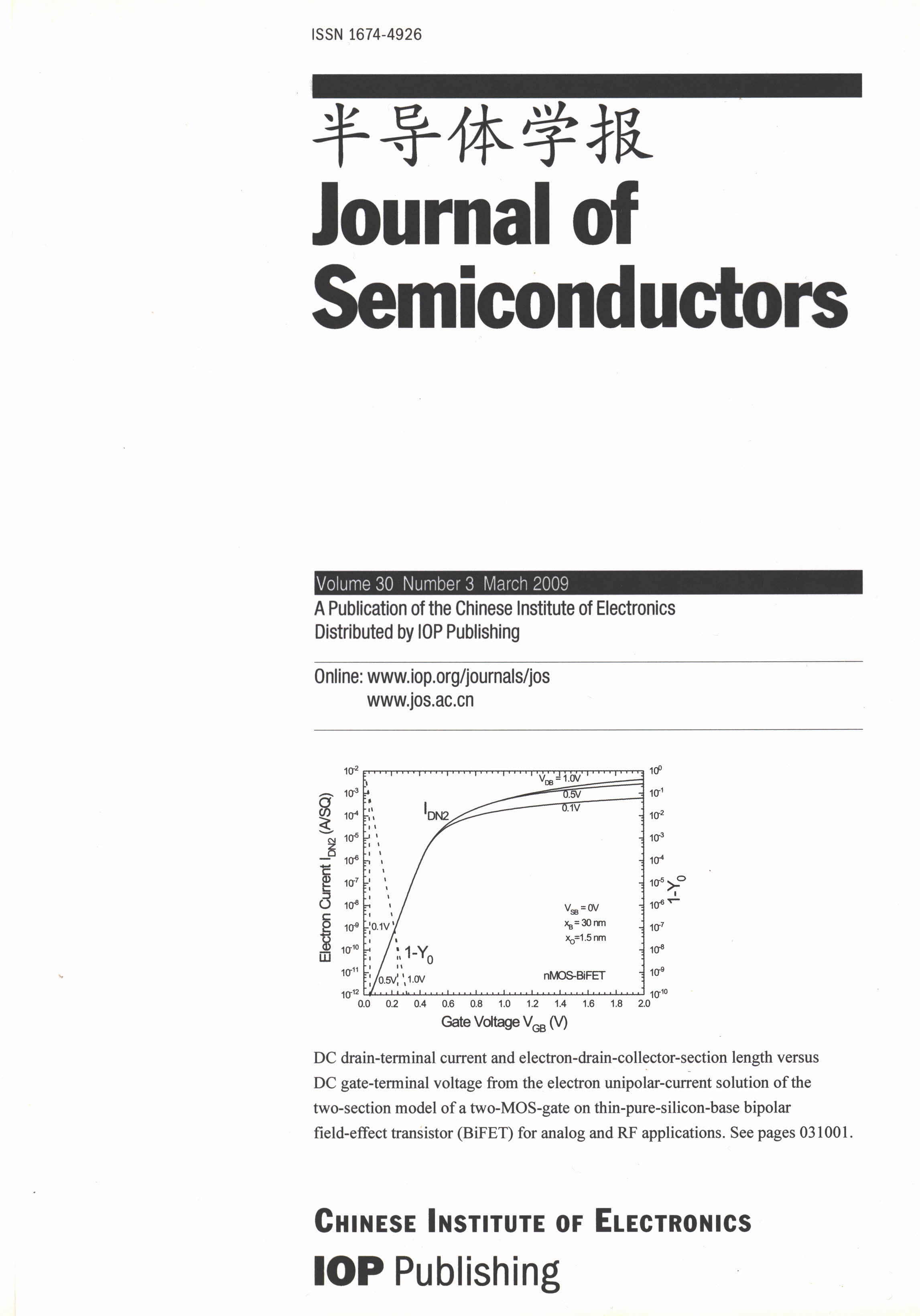
This paper reports the DC steady-state current–voltage and conductance–voltage characteristics of a Bipolar Field-Effect Transistor (BiFET) under the unipolar (electron) current mode of operation, with bipolar (electron and hole) charge distributions considered. The model BiFET example presented has two MOS-gates on the two surfaces of a thin pure silicon base layer with electron and hole contacts on both edges of the thin base. The hole contacts on both edges of the thin pure base layer are grounded to give zero hole current. This 1-transistor analog-RF Basic Building Block nMOS amplifier circuit, operated in the unipolar current mode, complements the 1-transistor digital Basic Build Block CMOS voltage inverter circuit, operated in the bipolar-current mode just presented by us.
The properties of interface polarons in a strained (111)-oriented zinc-blende GaN/AlxGa1-xN heterojunction at finite temperature under hydrostatic pressure are investigated by adopting a modified LLP variational method and a simplified coherent potential approximation. Considering the effect of hydrostatic pressure on the bulk longitudinal optical phonon mode, two branches interface-optical phonon modes and strain, respectively, we calculated the polaronic self-trapping energy and effective mass as functions of temperature, pressure and areal electron density. The numerical result shows that both of them near linearly increase with pressure but the self-trapping energies are nonlinear monotone increasing with increasing of the areal electron density. They are near constants below a range of temperature whereas decrease dramatically with increasing temperature beyond the range. The contributions from the bulk longitudinal optical phonon mode and one branch of interface optical phonon mode with higher frequency are important whereas the contribution from another branch of interface optical phonon mode with lower frequency is extremely small so that it can be neglected in the further discussion.
Using NH3 as nitrogen source gas, N-doped ZnO (ZnO:N) thin films in c-axis orientation were deposited on glass substrates by radio frequency magnetron sputtering at room temperature. The ZnO:N thin films display significant increase of resistivity and decrease of photoluminescence intensity. As-grown ZnO:N material was used as active channel layer and Si3N4 was used as gate insulator to fabricate thin-film transistor. The fabricated devices on glasses demonstrate typical field effect transistor characteristics.
Double-layered, low-voltage ZnO varistors have been fabricated by feeding two kinds of ZnO powders into a die using dry extrusion molding. Compared with ZnO varistors fabricated by the conventional route, the layered ZnO varistors have larger non-linear coefficients, lower breakdown electric fields, and lower leakage current densities. The improvement in electrical performance of the layered low-voltage ZnO varistors is attributed to the asymmetric band structure at grain boundary between the two layers.
Unintentionally doped 4H-SiC homoepitaxial layers grown by hot-wall chemical vapor deposition (HWCVD) have been studied using photoluminescence (PL) technique in the temperature range of 10 to 240 K. A broadband green luminescence has been observed. Vacancies of carbon (VC) are revealed by electron spin resonance (ESR) technique at 110 K. The results strongly suggest that the green band luminescence, as shallow donor-deep accepter emission, is attributed to the vacancies of C and the extended defects. The broadband green luminescence spectrum can be fitted by the two Gauss-type spectra using nonlinear optimization technique. It shows that the broad-band green luminescence originates from the combination of two independent radiative transitions. The centers of two energy levels are located 2.378 and 2.130 eV below the conduction band, respectively, and the ends of two energy levels are expanded and superimposed each other.
We report optical and electrical properties of polycrystalline GaSb thin films which were successfully grown by co-evaporation on soda-lime glass substrates. The thin films have preferential orientation of the (111) direction. SEM results indicate that the average grain size of GaSb thin film is 500 nm with the substrate temperature of 560 ℃. The average reflectance of GaSb thin film is about 30% and the absorption coefficient is of the order of 104 cm-1. The optical bandgap of GaSb thin film is 0.726 eV. The hole concentration shows a clear increasing trend as the Ga-evaporation-temperature/ Sb-evaporation-temperature (TGa/TSb) ratio increases. When the Ga crucible temperature is 810 ℃ and the antinomy crucible temperature is 415 ℃, the hole concentration of polycrystalline GaSb is 2 × 1017 cm-3 and the hole mobility is 130 cm2/(V·s). These results suggest that polycrystalline GaSb thin film is a good candidate for the use as a cheap material in TPV cells.
The CF2 density and etch rate of SiO2, Si3N4 and Si are investigated as a function of gas pressure and O2 flow rate in fluorocarbon plasma. As the pressure increases, the self-bias voltage decreases whereas the SiO2 etch rate increases. Previous study has shown that SiO2 etch rate is proportional to the self-bias voltage. This result indicates that other etching parameters contribute to the SiO2 etching. Generally, the CF2radical is considered as a precursor for fluorocarbon layer formation. At a given power, defluorination of fluorocarbon under high-energy ion bombardment is a main source of fluorine for SiO2 etching. When more CF2 radical in plasma, SiO2 etch rate is increased because more fluorine can be provided. In this case, CF2 is considered as a reactant for SiO2 etching. The etch rate of Si3N4 and Si is mainly determined by the polymer thickness formed on its surface which is dominated by the CF2 density in plasma. Etching results obtained by varying O2 flow rate also support the proposition.
Electromigration (EM) behavior of Cu/Sn3:5Ag/Cu solder reaction couple was investigated with a high current density of 5 × 10³ A/cm2 at room temperature. One dimensional structure, copper wire/solder ball/copper wire SRC was designed and fabricated to dissipate the Joule heating induced by the current flow. In addition, thermomigration effect was excluded due to the symmetrical structure of the SRC. The experimental results indicated that micro-cracks initially appeared near the cathode interface between solder matrix and copper substrate after 474 h current stressing. With current stressing time increased, the cracks propagated and extended along the cathode interface. It should be noted that the continuous Cu6Sn5 intermetallic compounds (IMCs) layer both at the anode and at the cathode remained their sizes. Interestingly, tiny cracks appeared at the root of some long column-type Cu6Sn5 at the cathode interface due to the thermal stress.
High-temperature characteristics of the metal/AlxGa1–xN
This paper investigates the capacitance–voltage (C–V) measurement on fully silicided (FUSI) gated metal-oxide-semiconductor (MOS) capacitors and the applicability of MOS capacitor models. When the oxide leakage current of an MOS capacitor is large, two-element parallel or series model cannot be used to obtain its real C–V characteristic. A three-element model simultaneously consisting of parallel conductance and series resistance or a four-element model with further consideration of a series inductance should be used. We employed the three-element and the four-element models with the help of two-frequency technique to measure the Ni FUSI gated MOS capacitors. The results indicate that the capacitance of the MOS capacitors extracted by the three-element model still shows some frequency dispersion, while that extracted by the four-element model is close to the real capacitance, showing little frequency dispersion. The obtained capacitance can be used to calculate the dielectric thickness with quantum effect correction by NCSUC–V program. We also investigated the influence of MOS capacitor's area on the measurement accuracy. The results indicate that the decrease of capacitor area can reduce the dissipation factor and improve the measurement accuracy. As a result, the frequency dispersion of the measured capacitance is significantly reduced, and real C–V characteristic can be obtained directly by the series model. In addition, this paper investigates the quasi-static C–V measurement and the photonic high-frequency C–V measurement on Ni FUSI metal gated MOS capacitor with a thin leaky oxide. The results indicate that the large tunneling current through the gate oxide significantly perturbs the accurate measurement of the displacement current, which is essential for the quasi-static C–V measurement. On the other hand, the photonic high-frequency C–V measurement can bypass the leakage problem, and get reliable low-frequency C–V characteristic, which can be used to evaluate whether the full silicidation has completed or not, and to extract the interface trap density of the SiO2/Si interface.
Silicide-block-film effects on drain-extended MOS (DEMOS) transistors were comparatively investigated, by means of different film stack stoichiometric SiO2 and silicon-rich oxide (SRO). The electrical properties of the as-deposited films were evaluated by extracting source/drain series resistance. It was found that the block film plays a role like a field plate, which has significant influence on the electric field beneath. Similar to hot-carrier-injection (HCI) induced degradation for devices, the block film initially charged in fabrication process also strongly affects the device characteristics and limits the safe operating area.
Two layout and process key parameters for improving high voltage nLEDMOS (n-type lateral extended drain MOS) transistor hot carrier performance have been identified. Increasing the space between Hv-pwell and n-drift region and reducing the n-drift implant dose can dramatically reduce the device hot carrier degradations, for the maximum impact ionization rate near the Bird Beak decreases or its location moves away from the Si/SiO2 interface. This conclusion has been analyzed in detail by using the MEDICI simulator and it is also confirmed by the test results.
A new quite simple analytical model based on the charge allocating approach has been proposed to describe the breakdown property of the RESURF (reduced surface field) structure. It agrees well with the results of numerical simulation on predicting the breakdown voltage. Compared with the latest published analytical model, this model has a better accuracy according to the numerical simulation with simpler form. The optimal doping concentration (per unit area) of the epi-layer of the RESURF structures with different structure parameters has been calculated based on this model and the results show no significant discrepancy to the data gained by others.Additionally the physical mechanism of how the surface field is reduced is clearly illustrated by this model.
This paper presents the benchmark test results on the symmetry and continuity characteristics between BSIM4 from Berkeley and ULTRA-BULK from Peking University. It is shown that the industry standard model BSIM4 has a series of the shortcomings of the continuity and symmetry, such as the charge, high-order current derivatives, and the trans-capacitances while the latest advanced surface-potential based MOSFET compact model, ULTRA-BULK, demonstrates all necessary continuity and symmetry characteristics, which are very important for analog and RF circuit design.
Hydrogenated microcrystalline silicon ( c-Si:H) intrinsic films and solar cells with n–i–p configuration were prepared by plasma enhanced chemical vapor deposition (PECVD). The influence of n/i and i/p buffer layers on the c-Si:H cell performance was studied in detail. The experimental results demonstrated that the efficiency is much improved when there is a higher crystallinity at n/i interface and an optimized a-Si:H buffer layer at i/p interface. By combining the above methods, the performance of c-Si:H single-junction and a-Si:H/ c-Si:H tandem solar cells has been significantly improved.
The comb capacitances fabricated by deep reactive ion etching (RIE) process have high aspect ratio which is usually smaller than 30 : 1 for the complicated process factors, and the combs are usually not parallel due to the well-known micro-loading effect and other process factors, which restricts the increase of the seismic mass by increasing the thickness of comb to reduce the thermal mechanical noise and the decrease of the gap of the comb capacitances for increasing the sensitive capacitance to reduce the electrical noise. Aiming at the disadvantage of the deep RIE, a novel capacitive micro-accelerometer with grid strip capacitances and sensing gap alterable capacitances is developed. One part of sensing of inertial signal of the micro-accelerometer is by the grid strip capacitances whose overlapping area is variable and which do not have the non-parallel plate's effect caused by the deep RIE process. Another part is by the sensing gap alterable capacitances whose gap between combs can be reduced by the actuators. The designed initial gap of the alterable comb capacitances is relatively large to depress the effect of the maximum aspect ratio (30 : 1) of deep RIE process. The initial gap of the capacitance of the actuator is smaller than the one of the comb capacitances. The difference between the two gaps is the initial gap of the sensitive capacitor. The designed structure depresses greatly the requirement of deep RIE process. The effects of non-parallel combs on the accelerometer are also analyzed. The characteristics of the micro-accelerometer are discussed by field emission microscopy (FEM) tool ANSYS. The tested devices based on slide-film damping effect are fabricated, and the tested quality factor is 514, which shows that grid strip capacitance design can partly improve the resolution and also prove the feasibility of the designed silicon-glass anodically bonding process.
Due to the difficulty in synthesizing perhalogenated metallophthalocyanine, the method of ammonium molybdate solid phase catalysis was introduced, and by using tetrachlorophthalic anhydride and urea as the raw materials, hexadecachloro zinc phthalocyanine (ZnPcCl16) was synthesized. Components of the composite were analyzed by energy spectrum, and its functional group structures and absorption peaks were characterized by IR and UV-vis spectroscopy. The thin films of gas sensors were prepared in a vacuum evaporation system and evaporated onto SiO2 substrates, where sensing electrodes were made by MEMS micromachining. The optimal conditions for the films are: substrate temperature of 150 ℃ evaporation current of 95 A and film thickness of 50 nm. The result showed that the sensors were ideally sensitive to Cl2 gas and could detect the minimum concentration of 0.3 ppm.
Aiming at detecting Cl2 gas, this study was made on how to make In-based compound semiconductor oxide gas sensor. The micro-property and sensitivity of In-based gas sensing material were analyzed and its gas sensitive mechanism was also discussed. Adopting constant temperature chemical coprecipitation, the compound oxides such as In–Nb, In–Cd and In–Mg were synthesized, respectively. The products were sintered at 600 ℃ and characterized by the Scanning Electron Microscope (SEM), showing the grain size almost about 50–60 nm. The test results show that the sensitivities of In–Nb, In–Cd and In–Mg materials under the concentration of 50 × 10-6 in Cl2 gas are above 100 times, 4 times and 10 times, respectively. The response time of In–Nb, In–Cd and In–Mg materials is about 30, 60 and 30 s, and the recovery time less than 2, 10 and 2 min, respectively. Among them, the In–Nb material was found to have a relatively high conductivity and ideal sensitivity to Cl2 gas, which showed rather good selectivity and stability, and could detect the minimum concentration of 0.5 × 10⁻⁶ with the sensitivity of 2.2, and the upper limit concentration of 500 × 10-6. The power loss of the device is around 220 mW under the heating voltage of 3 V.
A voltage-controlled ring oscillator (VCO) based on a full enhancement-mode InAlAs/InGaAs/InP high electron mobility transistor (HEMT) logic is proposed. An enhancement-mode HEMT (E-HEMT) is fabricated, whose threshold is demonstrated to be 10 mV. The model of the E-HEMT is established and used in the SPICE simulation of the VCO. The result proves that the full E-HEMT logic technology can be applied to the VCO. And compared with the HEMT DCFL technology, the complexity of our fabrication process is reduced and the reliability is improved.
A broadband CMOS intermediate frequency (IF) variable-gain amplifier (VGA) for DRM/DAB tuners is presented. The VGA comprises two cascaded stages: one is for noise-canceling and another is for signal-summing. The chip is fabricated in a standard 0.18 μm 1P6M RF CMOS process of SMIC. Measured results show a good linear-in-dB gain characteristic in 28 dB dynamic gain range of –10 to 18 dB. It can operate in the frequency range of 30–700 MHz and consumes 27 mW at 1.8 V supply with the on-chip test buffer. The minimum noise figure is only 3.1 dB at maximum gain and the input-referred 1 dB gain compression point at the minimum gain is –3.9 dBm.
A receiver for SRDs implemented by the 0.35 μm CMOS process is presented. The receiver, together with the ADC, power amplifier (PA), frequency synthesizer and digital baseband has been integrated into a single chip solution. Low cost and low power requirements are met by optimizing the receiver architecture and circuit topology. A simple mixed-signal mode I/Q imbalance calibration circuit is proposed to enhance the IRR (image rejection ratio) so as to raise the BER. From a single 3 V power supply, the receiver consumes 5.9 mA. The measurement result shows that the receiver achieves reference sensitivity of –60 dBm and a control gain of 60 dB. The S11 reaches –20 dB at 433 MHz and –10 dB at 868 MHz without off-chip impedance match network. The die area is only 2 mm2 including the bias circuit.
An on-chip microelectromechanical system was fabricated in a 0.5 μm standard CMOS process for gas pressure detection. The sensor was based on a micro-hotplate (MHP) and had been integrated with a rail to rail operational amplifier and an 8-bit successive approximation register (SAR) A/D converter. A tungsten resistor was manufactured on the MHP as the sensing element, and the sacrificial layer of the sensor was made from polysilicon and etched by surface-micromachining technology. The operational amplifier was configured to make the sensor operate in constant current mode. A digital bit stream was provided as the system output. The measurement results demonstrate that the gas pressure sensitive range of the vacuum sensor extends from 1 to 105 Pa. In the gas pressure range from 1 to 100 Pa, the sensitivity of the sensor is 0.23 mV/ Pa, the linearity is 4.95%, and the hysteresis is 8.69%. The operational amplifier can drive 200 Ω resistors distortionlessly, and the SAR A/D converter achieves a resolution of 7.4 bit with 100 kHz sample rate. The performance of the operational amplifier and the SAR A/D converter meets the requirements of the sensor system.
A novel low power RF receiver front-end for 3–5 GHz UWB is presented. Designed in the 0.13 μm CMOS process, the direct conversion receiver features a wideband balun-coupled noise cancelling transconductance input stage, followed by quadrature passive mixers and transimpedance loading amplifiers. Measurement results show that the receiver achieves an input return loss below 8.5 dB across the 3.1–4.7 GHz frequency range, max-imum voltage conversion gain of 27 dB, minimum noise figure of 4 dB, IIP3 of –11.5 dBm, and IIP2 of 33 dBm. Working under 1.2 V supply voltage, the receiver consumes total current of 18 mA including 10 mA by on-chip quadrature LO signal generation and buffer circuits. The chip area with pads is 1.1 × 1.5 mm2.
A new low-voltage CMOS bandgap reference (BGR) that achieves high temperature stability is proposed. It feeds back the output voltage to the curvature compensation circuit that constitutes a closed loop circuit to cancel the logarithmic term of voltage VBE. Meanwhile a low voltage amplifier with the 0.5 μm low threshold technology is designed for the BGR. A high temperature stability BGR circuit is fabricated in the CSMC 0.5 μm CMOS technology. The measured result shows that the BGR can operate down to 1 V, while the temperature coefficient and line regulation are only 9 ppm/℃ and 1.2 mV/V, respectively.
Due to aggressive technology scaling, radiation-induced soft errors have become a serious reliability concern in VLSI chip design. This paper presents a novel radiation hardened by design latch with high single-event-upset (SEU) immunity. The proposed latch can effectively mitigate SEU by internal dual interlocked scheme. The propagation delay, power dissipation and power delay product of the presented latch are evaluated by detailed SPICE simulations. Compared with previous SEU-hardening solutions such as TMR-Latch, the presented latch is more area efficient, delay and power efficient. Fault injection simulations also demonstrate the robustness of the presented latch even under high energy particle strikes.
A novel power supply transform technique for high voltage IC based on the TSMC 0.6 μm BCD process is achieved. An adjustable bandgap voltage reference is presented which is different from the traditional power supply transform technique. It can be used as an internal power supply for high voltage IC by using the push-pull output stage to enhance its load capability. High-order temperature compensated circuit is designed to ensure the precision of the reference. Only 0.01 mm2 area is occupied using this novel power supply technique. Compared with traditional technique, 50% of the area is saved, 40% quiescent power loss is decreased, and the temperature coefficient of the reference is only 4.48 ppm/℃. Compared with the traditional LDO (low dropout) regulator, this power conversion architecture does not need external output capacitance and decreases the chip-pin and external components, so the PCB area and design cost are also decreased. The testing results show that this circuit works well.