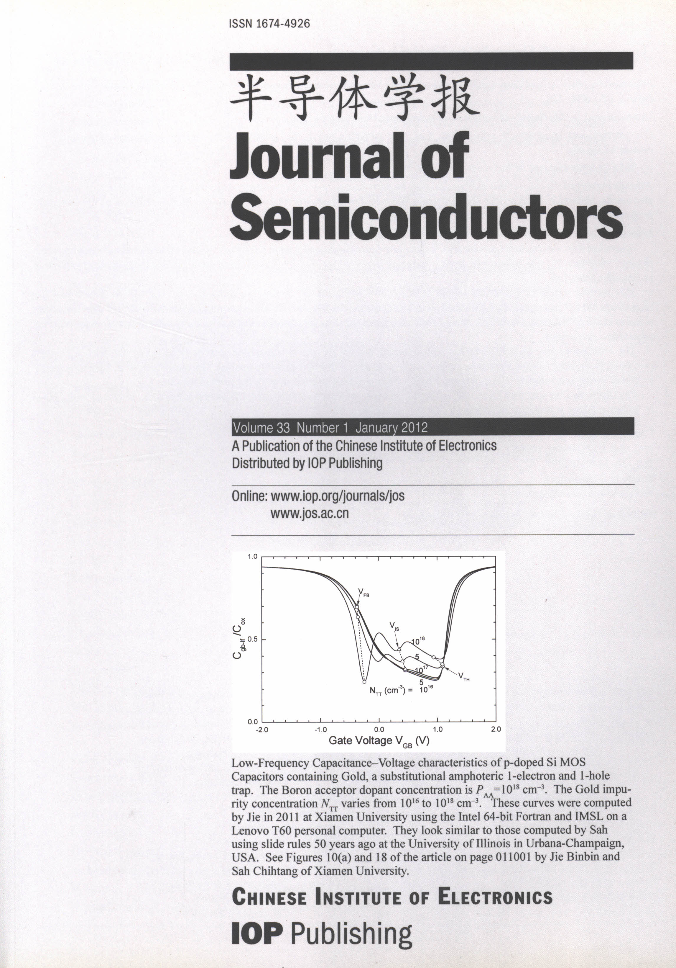
Metal-Oxide-Semiconductor Capacitance-Voltage (MOSCV) characteristics containing giant carrier trapping capacitances from 3-charge-state or 2-energy-level impurities are presented for not-doped, n-doped, p-doped and compensated silicon containing the double-donor sulfur and iron, the double-acceptor zinc, and the amphoteric or one-donor and one-acceptor gold and silver impurities. These impurities provide giant trapping capacitances at trapping energies from 200 to 800 meV (50 to 200 THz and 6 to 1.5 μm), which suggest potential sub-millimeter, far-infrared and spin electronics applications.
Issue Browser
Volume 33, Issue 1,
Jan 2012
J. Semicond.
2012, 33(1): 012001 doi: 10.1088/1674-4926/33/1/012001
Effect of rhenium doping is examined in single crystals of MoSe2 viz. MoRe0.005Se1.995, MoRe0.001Se1.999 and Mo0.995Re0.005Se2, which is grown by using the direct vapor transport (DVT) technique. The grown crystals are structurally characterized by X-ray diffraction, by determining their lattice parameters a and c, and X-ray density. Also, the Hall effect and thermoelectric power (TEP) measurements show that the single crystals exhibit a p-type semiconducting nature. The direct and indirect band gap measurements are also undertaken on these semiconducting materials.
J. Semicond.
2012, 33(1): 012002 doi: 10.1088/1674-4926/33/1/012002
Crystal structures and electronic structures of hafnium doping anatase TiO2 were calculated by first principles with the plane-wave ultrasoft pseudopotential method based on the density functional theory within the generalized gradient approximation. The calculated results show that the lattice parameters a and c of Hf-doped anatase TiO2 are larger than those of intrinsic TiO2 under the same calculated condition. The calculated band structure and density of states show that the conduction band width of Hf-doped TiO2 is broadened which results in the band gap of Hf-doped being smaller than the band gap of TiO2.
J. Semicond.
2012, 33(1): 013001 doi: 10.1088/1674-4926/33/1/013001
The Fe-doped CuO nanopowder was synthesized by following the standard solid-state reaction method. The structure and magnetic properties of the Fe-doped CuO nanopowder were investigated. X-ray diffraction spectra confirmed the monoclinic structure of CuO and no secondary phase was detected, indicating that the Fe ions were incorporated into CuO. The ferromagnetism in Fe-doped CuO was studied and is believed to originate from the interaction between Fe ions and Cu ions via a super-exchange interaction or F-center mediated exchange interaction.
Effect of substrate temperature on the properties of deep ultraviolet transparent conductive ITO/Ga2
J. Semicond.
2012, 33(1): 013002 doi: 10.1088/1674-4926/33/1/013002
ITO/Ga2O3 bi-layer films were deposited on quartz glass substrates by magnetron sputtering. The effect of substrate temperature on the structure, surface morphology, optical and electrical properties of ITO/Ga2O3 films was investigated by an X-ray diffractometer, a scanning electron microscope, a double beam spectrophotometer and the Hall system, respectively. The structural characteristics showed a dependence on substrate temperature. The resistivity of the films varied from 6.71 × 10⁻³ to 1.91 × 10⁻³ Ω·cm as the substrate temperature increased from 100 to 350 ℃. ITO (22 nm)/Ga2O3 (50 nm) films deposited at 300 ℃ exhibited a low sheet resistance of 373.3 Ω/□ and high deep ultraviolet transmittance of 78.97% at the wavelength of 300 nm.
J. Semicond.
2012, 33(1): 013003 doi: 10.1088/1674-4926/33/1/013003
We report Al/MoO3 thin film used as a complex anode in high-performance OLEDs. The unique efficacy of the device was found to result from the enhanced injection of holes into the commonly used hole-transporting molecules due to a large reduction in the interface dipole at the anode/organic interface. The superior optical characteristics are attributed to a strong cavity effect, Due to the ease of processing Al/MoO3 we successfully demonstrated large-area flexible OLEDs on plastic substrates with uniform emission.
J. Semicond.
2012, 33(1): 014001 doi: 10.1088/1674-4926/33/1/014001
We have studied the influence of hot-carrier degradation effects on the drain current of a gate-stack double-gate (GS DG) MOSFET device. Our analysis is carried out by using an accurate continuous current-voltage (I-V) model, derived based on both Poisson's and continuity equations without the need of charge-sheet approximation. The developed model offers the possibility to describe the entire range of different regions (subthreshold, linear and saturation) through a unique continuous expression. Therefore, the proposed approach can bring considerable enhancement at the level of multi-gate compact modeling including hot-carrier degradation effects.
J. Semicond.
2012, 33(1): 014002 doi: 10.1088/1674-4926/33/1/014002
We studied the performance of AlGaN/GaN double heterojunction high electron mobility transistors (DH-HEMTs) with an AlGaN buffer layer, which leads to a higher potential barrier at the backside of the two-dimensional electron gas channel and better carrier confinement. This, remarkably, reduces the drain leakage current and improves the device breakdown voltage. The breakdown voltage of AlGaN/GaN double heterojunction HEMTs (~ 100 V) was significantly improved compared to that of conventional AlGaN/GaN HEMTs (~ 50 V) for the device with gate dimensions of 0.5 × 100 μ m and a gate-drain distance of 1 μ m. The DH-HEMTs also demonstrated a maximum output power of 7.78 W/mm, a maximum power-added efficiency of 62.3% and a linear gain of 23 dB at the drain supply voltage of 35 V at 4 GHz.
J. Semicond.
2012, 33(1): 014003 doi: 10.1088/1674-4926/33/1/014003
We report a high power Ku band internally matched power amplifier (IMPA) with high power added efficiency (PAE) using 0.3 μm AlGaN/GaN high electron mobility transistors (HEMTs) on 6H-SiC substrate. The internal matching circuit is designed to achieve high power output for the developed devices with a gate width of 4 mm. To improve the bandwidth of the amplifier, a T type pre-matching network is used at the input and output circuits, respectively. After optimization by a three-dimensional electromagnetic (3D-EM) simulator, the amplifier demonstrates a maximum output power of 42.5 dBm (17.8 W), PAE of 30% to 36.4% and linear gain of 7 to 9.3 dB over 13.8-14.3 GHz under a 10% duty cycle pulse condition when operated at Vds = 30 V and Vgs = -4 V. At such a power level and PAE, the amplifier exhibits a power density of 4.45 W/mm.
J. Semicond.
2012, 33(1): 014004 doi: 10.1088/1674-4926/33/1/014004
An InGaAs/InP DHBT with an InGaAsP composite collector is designed and fabricated using triple mesa structural and planarization technology. All processes are on 3-inch wafers. The DHBT with an emitter area of 1 × 15 μm2 exhibits a current cutoff frequency ft = 170 GHz and a maximum oscillation frequency fmax = 256 GHz. The breakdown voltage is 8.3 V, which is to our knowledge the highest BV_CEO ever reported for InGaAs/InP DHBTs in China with comparable high frequency performances. The high speed InGaAs/InP DHBTs with high breakdown voltage are promising for voltage-controlled oscillator and mixer applications at W band or even higher frequencies.
J. Semicond.
2012, 33(1): 014005 doi: 10.1088/1674-4926/33/1/014005
The impacts of substrate parasitic resistance and drain ballast resistance on electrostatic discharge (ESD) robustness of LDMOS are analyzed. By increasing the two parasitic resistances, the ESD robustness of LDMOS are significantly improved. The proposed structures have been successfully verified in a 0.35 μm BCD process without using additional process steps. Experimental results show that the second breakdown current of the optimal structure increases to 3.5 A, which is about 367% of the original device.
J. Semicond.
2012, 33(1): 014006 doi: 10.1088/1674-4926/33/1/014006
Total dose irradiation and the hot-carrier effects of sub-micro NMOSFETs are studied. The results show that the manifestations of damage caused by these two effects are quite different, though the principles of damage formation are somewhat similar. For the total dose irradiation effect, the most notable damage lies in the great increase of the off-state leakage current. As to the hot-carrier effect, most changes come from the decrease of the output characteristics curves as well as the decrease of trans-conductance. It is considered that the oxide-trapped and interface-trapped charges related to STI increase the current during irradiation, while the negative charges generated in the gate oxide, as well as the interface-trapped charges at the gate interface, cause the degradation of the hot-carrier effect. Different aspects should be considered when the device is generally hardened against these two effects.
J. Semicond.
2012, 33(1): 014007 doi: 10.1088/1674-4926/33/1/014007
A novel broad area slotted Fabry-Perot diode laser is designed and fabricated. Using a new semi-analytical method, we introduce effective refractive index perturbations in the form of etched slot features into a conventional 980 nm broad area Fabry-Perot cavity, and the spectral characteristics of the device are expected to be noticeably improved. A low density of slot features is formed by using standard optical lithography and inductively coupled plasma dry etching. The experimental results show that the full spectral width at half-maximum is less than 0.4 nm, meanwhile, the thermal shift of the emission spectrum is decreased from 0.26 to 0.07 nm/℃ over a temperature range of 10 to 60 ℃. The improved spectral characteristics of the device are proved to be attributed to such slotted Fabry-Perot laser structures.
J. Semicond.
2012, 33(1): 014008 doi: 10.1088/1674-4926/33/1/014008
This paper presents single event upset (SEU) and single event latch-up (SEL) characteristics of small feature size devices by laser backside testing method, which is dedicated to dealing with the increasing metal layers on the front side of integrated circuits. The influence of test data pattern on SEU threshold and cross-section is investigated. The supply current state of micro latch-up for deep sub-micron SRAM is described. The laser energy thresholds were correlated to heavy ion thresholds LET to determine an empirical relationship between laser energy threshold and heavy ion LET. This empirical relationship was used to estimate the equivalent laser LETs for devices fabricated in small feature sizes. Moreover, the SEU of a Power PC CPU fabricated with 90 nm SOI CMOS process has been tested, which indicates that the laser backside method could be used to evaluate SOI small feature size devices.
J. Semicond.
2012, 33(1): 014009 doi: 10.1088/1674-4926/33/1/014009
The extinction ratio (ER) of a Mach-Zehnder-interference (MZI) based silicon optical modulator can be strongly influenced by carrier absorption. Moreover, different doping positions can induce different distributions of injected carriers, leading to different ERs. This effect has been experimentally investigated based on the devices fabricated on silicon-on-insulator (SOI) by using a 0.18 μm CMOS process. Our experiments indicate that a device with a doping position of about 0.5 μm away from the edge of the rib waveguide has optimal ER.
J. Semicond.
2012, 33(1): 015001 doi: 10.1088/1674-4926/33/1/015001
A low-phase-noise Σ-Δ fractional-N frequency synthesizer for GSM/PCS/DCS/WCDMA transceivers is presented. The voltage controlled oscillator is designed with a modified digital controlled capacitor array to extend the tuning range and minimize phase noise. A high-resolution adaptive frequency calibration technique is introduced to automatically choose frequency bands and increase phase-noise immunity. A prototype is implemented in 0.13 μm CMOS technology. The experimental results show that the designed 1.2 V wideband frequency synthesizer is locked from 3.05 to 5.17 GHz within 30 μs, which covers all five required frequency bands. The measured in-band phase noise are -89, -95.5 and -101 dBc/Hz for 3.8 GHz, 2 GHz and 948 MHz carriers, respectively, and accordingly the out-of-band phase noise are -121, -123 and -132 dBc/Hz at 1 MHz offset, which meet the phase-noise-mask requirements of the above-mentioned standards.
J. Semicond.
2012, 33(1): 015002 doi: 10.1088/1674-4926/33/1/015002
A 1500 mA,10 MHz self-adaptive on-time (SOT) controlled buck DC-DC converter is presented. Both a low-cost ripple compensation scheme (RCS) and a self-adaptive on-time generator (SAOTG) are proposed to solve the system stability and frequency variation problem. Meanwhile a self-adaptive power transistor sizing (SAPTS) technique is used to optimize the efficiency especially with a heavy load. The circuit is implemented in a 2P4M 0.35 μ m CMOS process. A small external inductor of 0.47 μ H and a capacitor of 4.7 μ F are used to lower the cost of the converter and keep the output ripple to less than 10 mV. The measurement results show that the overshoot of the load transient response is 8 mV @ 200 mA step and the dynamic voltage scaling (DVS) performance is a rise of 16 μ s/V and a fall of 20 μ s/V. With a SAPTS technique and PFM control, the efficiency is maintained at more than 81% for a load range of 20 to 1500 mA and the peak efficiency reaches 88.43%.
J. Semicond.
2012, 33(1): 015003 doi: 10.1088/1674-4926/33/1/015003
This paper presents a wideband low noise amplifier (LNA) for multi-standard radio applications. The low noise characteristic is achieved by the noise-canceling technique while the bandwidth is enhanced by gate-inductive-peaking technique. High-frequency noise performance is consequently improved by the flattened gain over the entire operating frequency band. Fabricated in 0.18 μm CMOS process, the LNA achieves 2.5 GHz of -3 dB bandwidth and 16 dB of gain. The gain variation is within ± 0.8 dB from 300 MHz to 2.2 GHz. The measured noise figure (NF) and average IIP3 are 3.4 dB and -2 dBm, respectively. The proposed LNA occupies 0.39 mm2 core chip area. Operating at 1.8 V, the LNA drains a current of 11.7 mA.
J. Semicond.
2012, 33(1): 015004 doi: 10.1088/1674-4926/33/1/015004
A power-configurable high performance preamplifier was implemented in standard 180-nm CMOS technology for 12 × 10 Gb/s high-density ultra-high speed parallel optical communication system. With critical limitations on power consumption, area and fabrication cost, the preamplifier achieves high performance, e.g. high bandwidth, high trans-impedance gain, low noise and high stability. A novel feed-forward common gate (FCG) stage is adopted to alleviate contradictions on trans-impedance gain and bandwidth by using a low headroom consuming approach to isolate a large input capacitance and using complex pole peaking techniques to substitute inductors to achieve bandwidth extension. A multi-supply power-configurable scheme was employed to avoid wasteful power caused by a pessimistic estimation of process-voltage-temperature (PVT) variation. Two representative samples provide a trans-impedance gain of 53.9 dBΩ, a 3-dB bandwidth of 6.8 GHz, a power dissipation of 6.26 mW without power-configuration and a trans-impedance gain of 52.1 dBΩ, a 3-dB bandwidth of 8.1 GHz, a power dissipation of 6.35 mW with power-configuration, respectively. The measured average input-referred noise-current spectral density is no more than 28 pA/Hz. The chip area is only 0.08 ? 0.08 mm2.
J. Semicond.
2012, 33(1): 015005 doi: 10.1088/1674-4926/33/1/015005
A design of \,high dynamic range linear radio frequency power detector (PD), aimed for transmitter carrier leakage suppression is presented in this paper. Based on the logarithmic amplifier principle, this detector utilizes the successive detection method to achieve a high dynamic range in the radio frequency band. In order to increase sensitivity, a low noise amplifier (LNA) is placed in the front of this detector. DC coupling is adopted in this architecture to reduce parasitics and save area, but this will unavoidably cause DC offsets in the circuit which are detrimental to the dynamic range. So a DC offset cancelling (DCOC) technique is proposed to solve the problem. Finally, this detector was fabricated in the SMIC 0.13 μm CMOS process. The measured results show that it achieves a wide dynamic range of 50 dB/40 dB with log errors in ±1 dB at 900 MHz/2 GHz, while draws 16 mA from a 1.5 V power supply. The active chip area is 0.27 × 0.67 mm2.
J. Semicond.
2012, 33(1): 015006 doi: 10.1088/1674-4926/33/1/015006
This paper presents the design of 0.5 V multi-gigahertz cascode CMOS LNA for low power wireless communication. By splitting the direct current through conventional cascode topology, the constraint of stacking-MOS structure for supply voltage has been removed and based on forward-body-bias technology, the circuit can operate at 0.5 V supply voltage. Design details and RF characteristics have been investigated in this paper. To verify the investigation, a 0.5 V 5.4 GHz LNA has been fabricated through 0.18 μm CMOS technology and measured. Measured results show that it obtains 9.1 dB gain, 3 dB NF with 0.5 V voltage and 2.5 mW power dissipation. The measured IIP3 is -3.5 dBm. Compared with previously published cascode LNA, it achieves the lowest supply voltage and lowest power dissipation with competitive RF performances.
J. Semicond.
2012, 33(1): 015007 doi: 10.1088/1674-4926/33/1/015007
A fourth-order continuous-time sigma delta modulator with 20-MHz bandwidth, implemented in 130-nm CMOS technology is presented. The modulator is comprised of an active-RC operational-amplifier based loop filter, a 4-bit internal quantizer and three current steering feedback DACs. A three-stage amplifier with low power is designed to satisfy the requirement of high dc gain and high gain-bandwidth product of the loop filter. Non-return-to-zero DAC pulse shaping is utilized to reduce clock jitter sensitivity. A special layout technique guarantees that the main feedback DAC reaches 12-bit match accuracy, avoiding the use of a dynamic element matching algorithm to induce excess loop delay. The experimental results demonstrate a 64.6-dB peak signal-to-noise ratio, and 66-dB dynamic range over a 20-MHz signal bandwidth when clocked at 480 MHz with 18-mW power consumption from a 1.2-V supply.
J. Semicond.
2012, 33(1): 015008 doi: 10.1088/1674-4926/33/1/015008
This paper presents a detailed description of a high-performance direct digital frequency synthesizer (DDFS) using optimized quarter ROMs. To improve the working frequency and spectral purity, an original quarter ROMs structure in 0.13 μm CMOS is brought forward and implemented. The working frequency is increased by 40% compared with Yuan Ling's method[1] of implementing a segmented DAC based DDFS. It has been implemented in 0.13 μm CMOS technology. The DDFS has a resolution of 10 bits with a measured SFDR 54 dBc. Its maximum operating frequency is 1.2 GHz by using six pipelining stages. Analytical investigation of improving spectral performances by using dual-slope approximation and pipeline is also presented.
J. Semicond.
2012, 33(1): 015009 doi: 10.1088/1674-4926/33/1/015009
A wideband variable gain amplifier (VGA) implemented in 0.13 μm CMOS technology is presented. To optimize noise performance, an active feedback amplifier with 15 dB fixed gain is put in the front, followed by modified Cherry-Hooper amplifiers in cascade providing variable gain, which adopt dual loop feedback for bandwidth extension. Negative capacitive neutralization and capacitive source degeneration are employed for Miller effect compensation and DC offset cancellation, respectively. Measurement results show that the proposed VGA achieves a 35 dB gain tuning range with an upper 3-dB bandwidth larger than 3 GHz and the input 1 dB compression point of -29 dBm at the lowest gain state, while the minimum noise figure is 9 dB at the highest gain state. The core VGA (without test buffer) consumes 32 mW from 1.2 V power supply and occupies 0.48 mm2 area.
J. Semicond.
2012, 33(1): 015010 doi: 10.1088/1674-4926/33/1/015010
We present an input/output block (IOB) array used in the radiation-hardened SRAM-based field-programmable gate array (FPGA) VS1000, which is designed and fabricated with a 0.5 μ m partially depleted silicon-on-insulator (SOI) logic process at the CETC 58th Institute. Corresponding with the characteristics of the FPGA, each IOB includes a local routing pool and two IO cells composed of a signal path circuit, configurable input/output buffers and an ESD protection network. A boundary-scan path circuit can be used between the programmable buffers and the input/output circuit or as a transparent circuit when the IOB is applied in different modes. Programmable IO buffers can be used at TTL/CMOS standard levels. The local routing pool enhances the flexibility and routability of the connection between the IOB array and the core logic. Radiation-hardened designs, including A-type and H-type body-tied transistors and special D-type registers, improve the anti-radiation performance. The ESD protection network, which provides a high-impulse discharge path on a pad, prevents the breakdown of the core logic caused by the immense current. These design strategies facilitate the design of FPGAs with different capacities or architectures to form a series of FPGAs. The functionality and performance of the IOB array is proved after a functional test. The radiation test indicates that the proposed VS1000 chip with an IOB array has a total dose tolerance of 100 krad(Si), a dose survivability rate of 1.5 × 10¹¹ rad(Si)/s, and a neutron fluence immunity of 1 × 10¹⁴ n/cm2.
J. Semicond.
2012, 33(1): 015011 doi: 10.1088/1674-4926/33/1/015011
An offset cancellation technique for a SAR (successive approximation register) ADC switched-capacitor comparator is described. The comparator is designed with a pre-amplifying and regenerative latching structure and realized in 0.18 μm CMOS. With the first stage preamplifier offset cancellation and low offset regenerative latching approach, the equivalent offset of the comparator is reduced to < 0.55 mV. By using the pre-amplifying and regenerative latching comparison mode the comparator exhibits low power dissipation. Under a 1.8 V power supply, with a 200 kS/s ADC sampling rate and 3 MHz clock frequency, a 13-bit comparison resolution is reached and less than 0.09 mW power dissipation is consumed. The superiority of this comparator is discussed and proved by the post-simulation and application to a 10 bit 200 kS/s touch screen SAR A/D converter.
J. Semicond.
2012, 33(1): 015012 doi: 10.1088/1674-4926/33/1/015012
This paper compares model differences of transformers measured in 4-port and 2-port configurations. Although 2-port configuration is more appropriate for measurement and application, it brings tremendous difficulties to the model's parameter extraction. In this paper, a physics-based equivalent circuit model and its corresponding direct extraction procedure are proposed for on-chip transformers. The extraction is based on the measurement of 2-port configuration instead of the 4-port type, and it can capture the model parameters without any optimization. In this procedure, a new method has been developed for the parameter extraction of the ladder circuit, which is commonly used to represent the skin effect. Thus, this method can be transferred to the modeling of other passive devices, such as on-chip transmission lines, inductors, baluns, etc. In order to verify the procedure's efficiency and accuracy, an on-chip interleaved transformer in a 90 nm 1P9M CMOS process has been fabricated. We compare the modeled and measured self-inductance, the quality factor, mutual reactive and resistive coupling coefficients. Excellent agreement has been found over a broad frequency range.