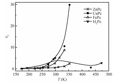
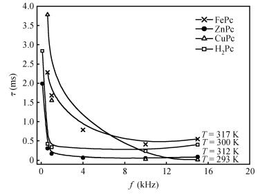
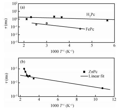
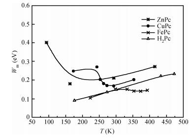
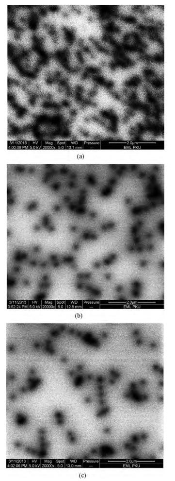
The AC-electronic and dielectric properties of different phthalocyanine films (ZnPc, CuPc, FePc, and H2Pc) were investigated over a wide range of temperature. Both real and imaginary parts of the dielectric constant (ε=ε1-iε2) were found to be influenced by temperature and frequency. Qualitatively the behavior was the same for those compounds; however, the central atom, film thickness, and the electrode type play an important role in the variation of their values.The relaxation time, τ, was strongly frequency-dependent at all temperatures and low frequencies, while a weak dependency is observed at higher frequencies. The relaxation activation energy was derived from the slopes of the fitted lines of ln τ and the reciprocal of the temperature (1/T). The values of the activation energy were accounted for the hopping process at low temperatures, while a thermally activated conduction process was dominant at higher temperatures.The maximum barrier height, Wm, was found to be temperature and frequency dependent for all phthalocyanine compounds. The value Wm depends greatly on the nature of the central atom and electrode material type. The correlated barrier hopping model was found to be the appropriate mechanism to describe the charge carrier's transport in phthalocyanine films.

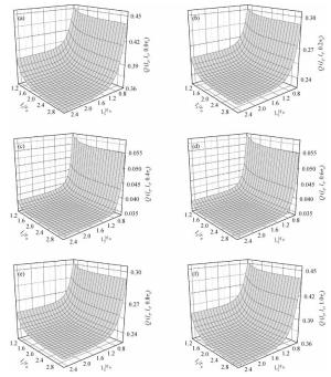
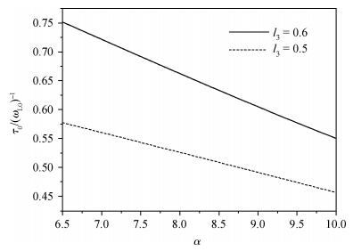
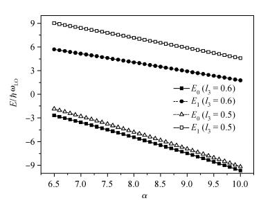
To study the influence of an anisotropic parabolic potential (APP) on the properties of a quantum dot (QD) qubit, we obtain the eigenenergies and eigenfunctions of the ground and first excited state of an electron, which is strongly coupled to the bulk longitudinal optical (LO) phonons, in a QD under the influence of an APP by the celebrated Lee-Low-Pines (LLP) unitary transformation and the Pekar type variational (PTV) methods. Then, this kind of two-level quantum system can be excogitated to constitute a single qubit. When the electron locates at the superposition state of its related eigenfunctions, we get the time evolution of the electron's probability density. Finally, the influence of an APP on the QD qubit is investigated. The numerical calculations indicate that the probability density will oscillate periodically and it is a decreasing function of the effective confinement lengths of the APP in different directions. Whereas its oscillatory period is an increasing one and will diminish with enhancing the electron-phonon (EP) coupling strength.

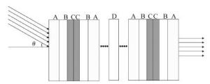
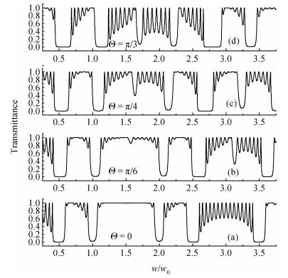
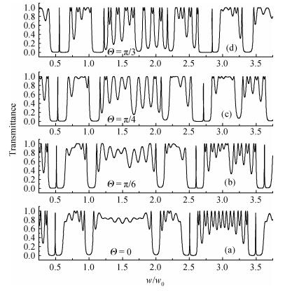
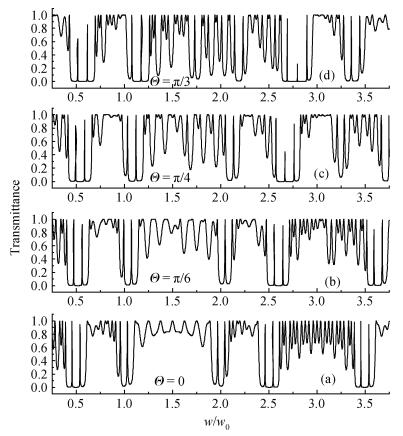
By means of a transfer matrix method, this paper deduces the transmittance calculation equation of light travelling in locally doped (including one defect layer) mirror heterostructure (ABCCBA)PD(ABCCBA)Q photonic crystals. In the cases of defect layers being either introduced or not introduced, an ORIGIN simulation shows the influence of incident angle change on the number of photon band gap, bandwidth and defect mode numbers. Studies indicate that when such photonic crystals have 8 mirror cycles and the thickness of defect layer D meets nDdD=λ 0/2 or nD dD=4λ 0, the photonic crystal defect mode transmission peak changes significantly. Also, with the change of incident angle, the number of defect mode transmission peaks changes. By altering incident angle and defect layer thickness, we can get photon band gaps and defect mode transmission peaks at different frequency domains and different relative angular frequencies. This provides theoretical reference for achieving light wave multi-channel filtering and tunable filtering.

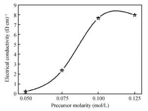
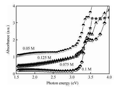
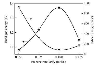
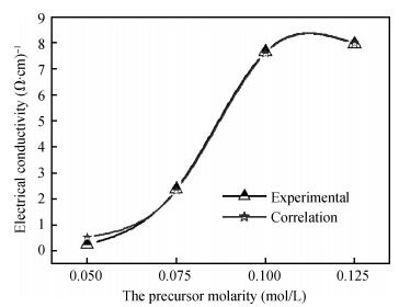
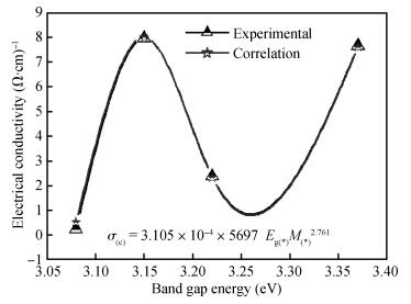
ZnO thin films were deposited using the simple, flexible and cost-effective spray ultrasonic technique at different precursor molarities values. The films were deposited on a glass substrate at 350℃. This paper is to present a new approach to the description of correlation between electrical conductivity and optical gap energy with precursor molarity of ZnO thin films. The ZnO films exhibit higher electrical n-type semiconductors, whose band gap energy increased from 3.08 to 3.37 eV with an increasing of precursor molarity of 0.05 to 0.1 M. The maximum value of electrical conductivity of the films is 7.96 (Ω·cm)-1 obtained in the ZnO thin film for precursor molarity 0.125 M. The correlation between the electrical and the optical properties with the precursor molarity suggests that the electrical conductivity of the films is predominantly influenced by the band gap energy and the precursor molarity. The measurement of the electrical conductivity of the films with correlation is equal to the experimental with the error is about 1% in the higher conductivity.

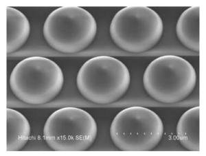
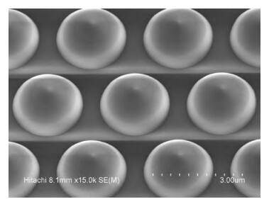
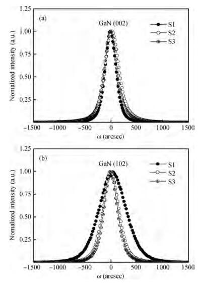
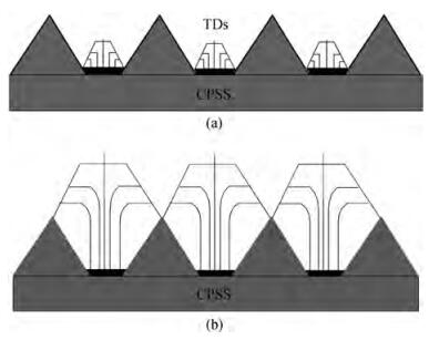
GaN films are grown on cone-shaped patterned sapphire substrates (CPSSs) by metal-organic chemical vapor deposition, and the influence of the temperature during the middle stage of GaN growth on the threading dislocation (TD) density of GaN is investigated. High-resolution X-ray diffraction (XRD) and cathode-luminescence (CL) were used to characterize the GaN films. The XRD results showed that the edge-type dislocation density of GaN grown on CPSS is remarkably reduced compared to that of GaN grown on conventional sapphire substrates (CSSs). Furthermore, when the growth temperature in the middle stage of GaN grown on CPSS decreases, the full width at half maximum of the asymmetry (102) plane of GaN is reduced. This reduction is attributed to the enhancement of vertical growth in the middle stage with a more triangular-like shape and the bending of TDs. The CL intensity spatial mapping results also showed the superior optical properties of GaN grown on CPSS to those of GaN on CSS, and that the density of dark spots of GaN grown on CPSS induced by nonradiative recombination is reduced when the growth temperature in the middle stage decreases.


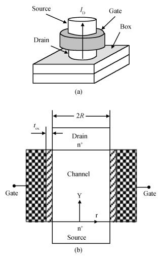
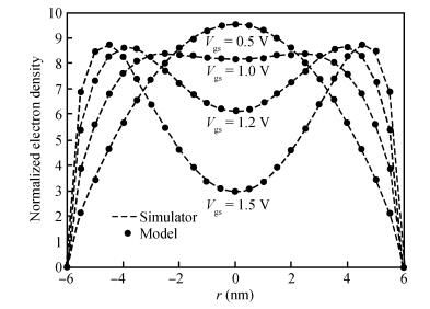
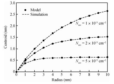
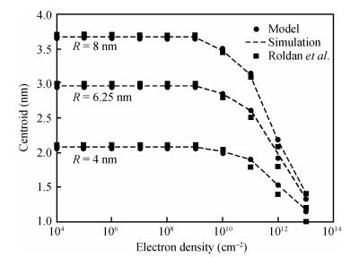
An analytical model for surrounding gate metal-oxide-semiconductor field effect transistors (MOSFETs) considering quantum effects is presented. To achieve this goal, we have used a variational approach for solving the Poission and Schrodinger equations. This model is developed to provide an analytical expression for the inversion charge distribution function for all regions of the device operation. This expression is used to calculate the other important parameters like the inversion charge centroid, threshold voltage and inversion charge density. The calculated expressions for the above parameters are simple and accurate. The validity of this model was checked for the devices with different device dimensions and bias voltages. The calculated results are compared with the simulation results and they show good agreement.


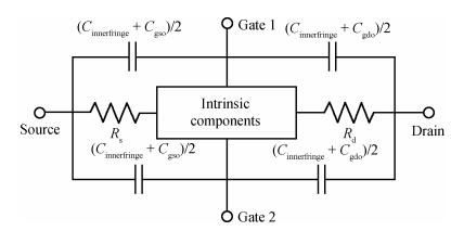
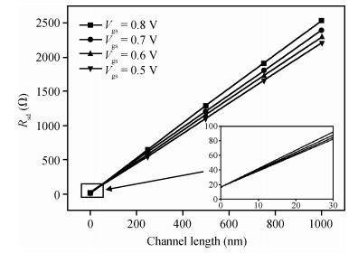
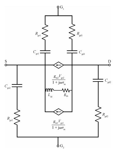
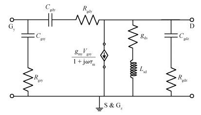
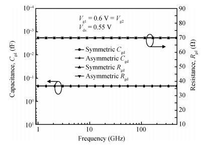
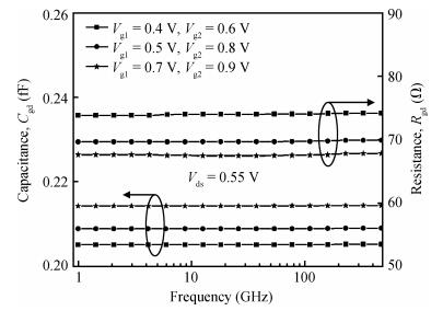
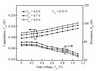
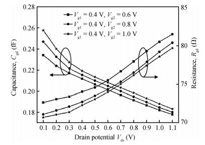
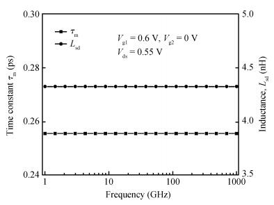
In analog circuit design an important parameter, from the perspective of superior device performance, is linearity. The DG MOSFET in asymmetric mode operation has been found to present a better linearity. In addition to that it provides, at the discretion of analog circuit designer, an additional degree of freedom, by providing independent bias control for the front and the back gates. Here a non-quasi-static (NQS) small signal model for DGMOSFET with asymmetric gate bias is proposed for extracting the parameters of the device using TCAD simulations. The parameters extracted here for analysis are the intrinsic front and back gate to drain capacitance, Cgd1 and Cgd2, the intrinsic front and back distributed channel resistance, Rgd1 and Rgd2 respectively, the transport delay, τm, and the inductance, Lsd. The parameter extraction model for an asymmetric DG MOSFET is validated with pre-established extracted parameter data, for symmetric DG MOSFET devices, from the available literature. The device simulation is performed with respect to frequency up to 100 GHz.
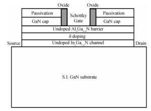
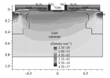
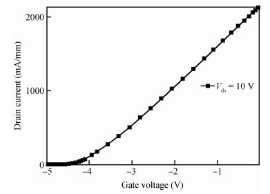
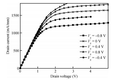
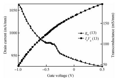
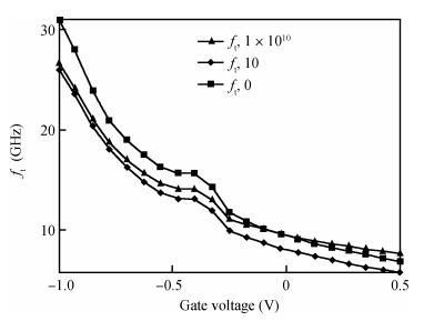
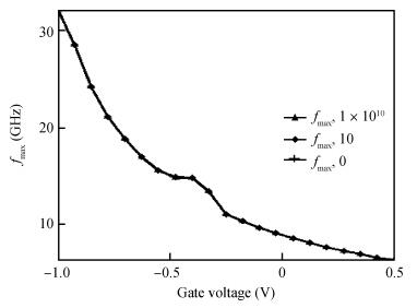
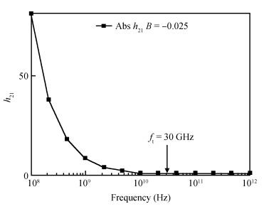
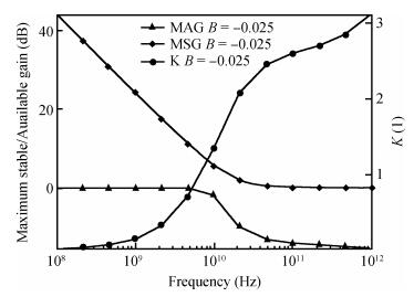
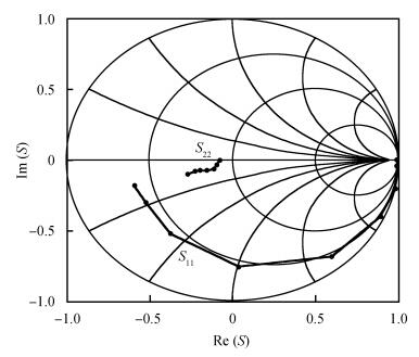
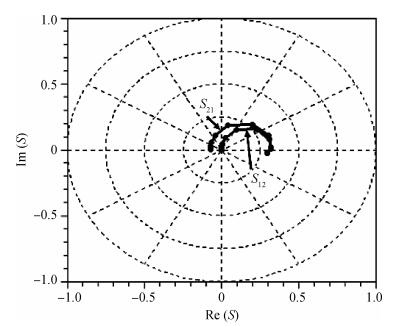
A new depletion-mode gate recessed AlGaN/InGaN/GaN-high electron mobility transistor (HEMT) with 10 nm thickness of InGaN-channel is proposed. A growth of AlGaN over GaN leads to the formation of two-dimensional electron gas (2DEG) at the heterointerface. High 2DEG density (ns) is achieved at the heterointerface due to a strain induced piezoelectric effect between AlGaN and GaN layers. The electrons are confined in the InGaN-channel without spilling over into the buffer layer, which also reduces the buffer leakage current. From the input transfer characteristics the threshold voltage is obtained as -4.5 V and the device conducts a current of 2 A/mm at a drain voltage of 10 V. The device also shows a maximum output current density of 1.8 A/mm at Vds of 3 V. The microwave characteristics like transconductance, cut-off frequency, max frequency of oscillation and Mason's Unilateral Gain of the device are studied by AC small-signal analysis using a two-port network. The stability and power performance of the device are analyzed by the Smith chart and polar plots respectively. To our knowledge this proposed InGaN-channel HEMT structure is the first of its kind.

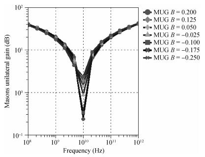

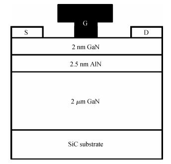
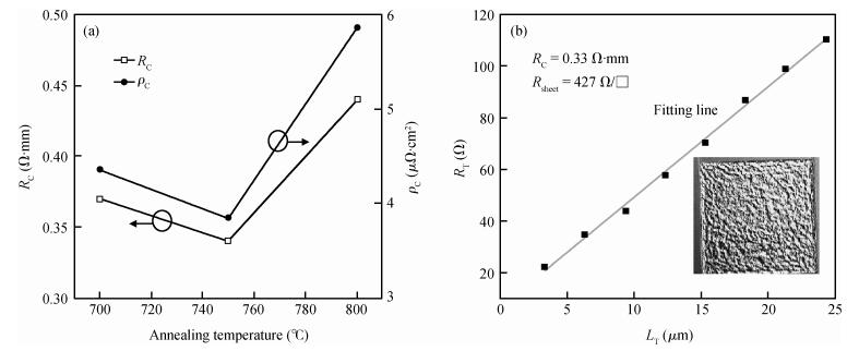
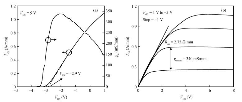
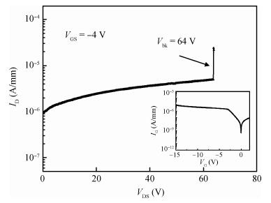
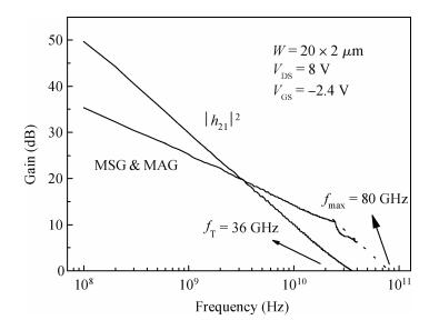
AlN/GaN high-electron-mobility transistors (HEMTs) on SiC substrates were fabricated by metal-organic chemical vapor deposition (MOCVD) and then characterized. An Si/Ti/Al/Ni/Au stack was used to reduce ohmic contact resistance (0.33 Ω· mm) at a low annealing temperature. The fabricated devices exhibited a maximum drain current density of 1.07 A/mm (VGS=1 V) and a maximum peak extrinsic transconductance of 340 mS/mm. The off-state breakdown voltage of the device was 64 V with a gate-drain distance of 1.9 μm. The current gain extrinsic cutoff frequency fT and the maximum oscillation frequency fmax were 36 and 80 GHz with a 0.25 μm gate length, respectively.
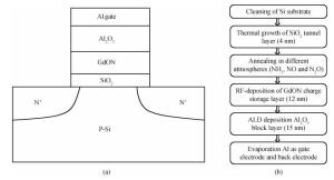
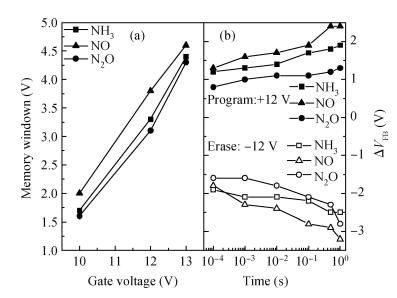
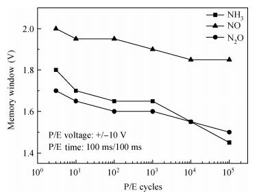
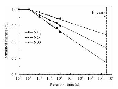
Metal-oxide-nitride-oxide-silicon (MONOS) capacitors with thermally grown SiO2 as the tunnel layer are fabricated, and the effects of different ambient nitridation (NH3, NO and N2O) on the characteristics of the memory capacitors are investigated. The experimental results indicate that the device with tunnel oxide annealed in NO ambient exhibits excellent memory characteristics, i.e. a large memory window, high program/erase speed, and good endurance and retention performance (the charge loss rate is 14.5% after 10 years). The mechanism involved is that much more nitrogen is incorporated into the tunnel oxide during NO annealing, resulting in a lower tunneling barrier height and smaller interface state density. Thus, there is a higher tunneling rate under a high electric field and a lower probability of trap-assisted tunneling during retention, as compared to N2O annealing. Furthermore, compared with the NH3-annealed device, no weak Si-H bonds and electron traps related to the hydrogen are introduced for the NO-annealed devices, giving a high-quality and high-reliability SiON tunneling layer and SiON/Si interface due to the suitable nitridation and oxidation roles of NO.

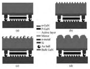
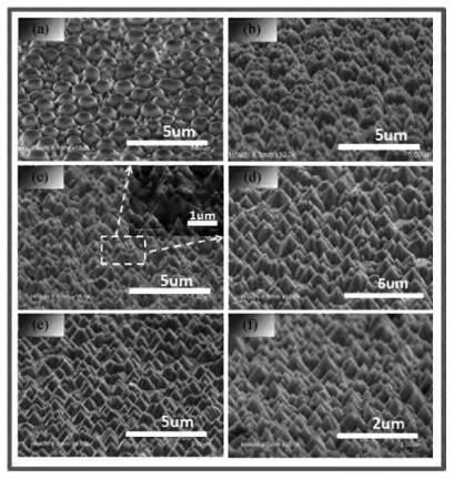
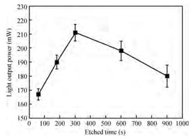
The light extraction enhancement of freestanding GaN-based flip-chip light-emitting diodes (FS-FCLEDs) using two-step roughening methods is investigated. The output power of LEDs fabricated by using one-step and two-step roughening methods are compared. The results indicate that two-step roughening methods show more potential for light extraction. Compared with flat FS-FCLEDs, the output power of FS-FCLEDs with a nanotextured hemisphere surface shows an enhancement of 90.7%.

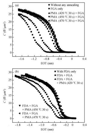
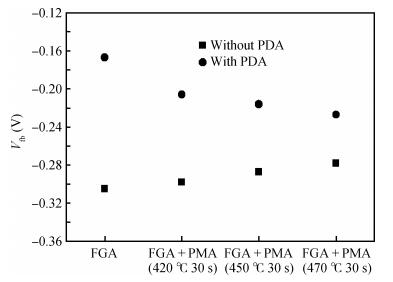
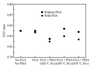
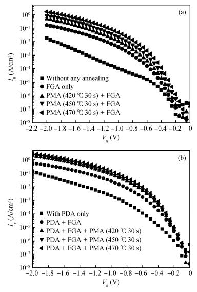
The effects of low temperature annealing, such as post high-k dielectric deposition annealing (PDA), post metal annealing (PMA) and forming gas annealing (FGA) on the electrical characteristics of a metal-oxide-semiconductor (MOS) capacitor with a TiN metal gate and a HfO2 dielectric are systematically investigated. It can be found that the low temperature annealing can improve the capacitance-voltage hysteresis performance significantly at the cost of increasing gate leakage current. Moreover, FGA could effectively decrease the interfacial state density and oxygen vacancy density, and PDA could make the flat band positively shift which is suitable for P-type MOSs.


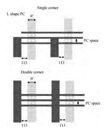
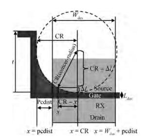
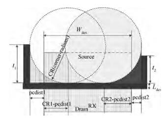
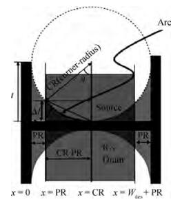
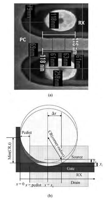
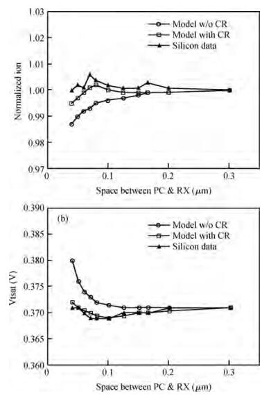
This paper presents a novel poly (PC) and active (RX) corner rounding modeling approach to SPICE simulations. A set of specially designed structures was used for measurement data collection. PC and RX corner rounding equations have been derived based on an assumption that the corner rounding area is a fragment of a circle. The equations were modified to reflect the gouging effect of physical silicon wafers. The modified general equations were implemented in the SPICE model to enable the model to describe the corner rounding effect. The good fittings between the SPICE model simulation results and the silicon data demonstrated in this paper proved that the designed corner rounding model is practical and accurate.

Based on the Arrhenius model, a rapid evaluation method for an infrared diode's normal lifetime is proposed, and the theoretical model is constructed. Accelerated life testing of an infrared light-emitting diode (IRLED), which takes less time than usual, is carried out under temperature and electric current stress. Using this method, the activation energy and the IRLED's normal lifetime are calculated and analyzed.


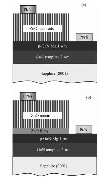
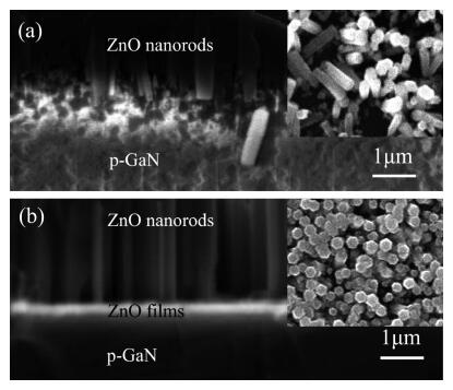
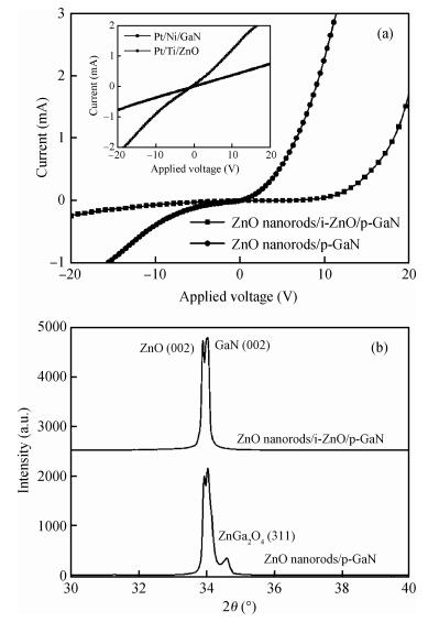
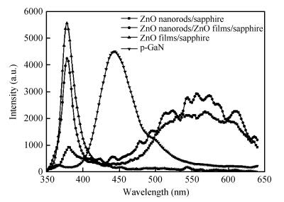
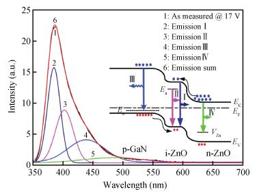
Heterostructure light-emitting diodes (LEDs) were fabricated by growing ZnO nanorods and undoped ZnO films on p-GaN templates. The heterojunction showed a diode-like I-V characteristic and emitted electroluminescence (EL) peaks at 383 nm, 402 nm, 438 nm, and 507 nm under forward bias. Since the electrons from ZnO nanorods and the holes from p-GaN could be injected into ZnO films with a relatively low carrier concentration and mobility, the radiative recombination was mainly confined in the ZnO film region. As a result, the ZnO nanorods/i-ZnO/p-GaN light emitting diode exhibits a stronger ultraviolet-violet emission peak.


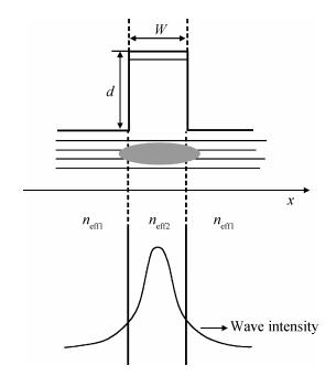
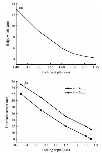
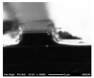
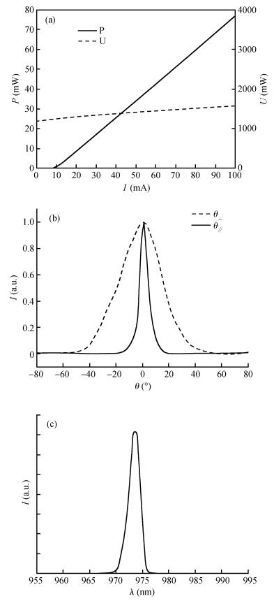
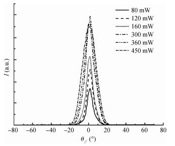
To achieve low threshold current as well as high single mode output power, a graded index separate confinement heterostructure (GRIN-SCH) AlGaInAs/AlGaAs quantum well laser with an optimized ridge waveguide was fabricated. The threshold current was reduced to 8 mA. An output power of 76 mW was achieved at 100 mA current at room temperature, with a slope efficiency of 0.83 W/A and a horizon divergent angle of 6.3°. The maximum single mode output power of the device reached as high as 450 mW.

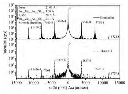
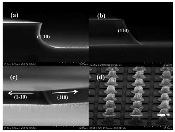
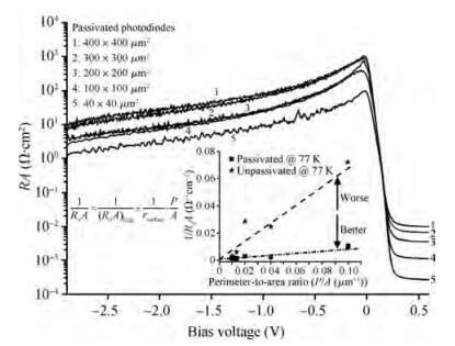
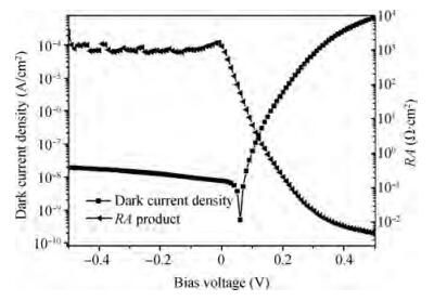
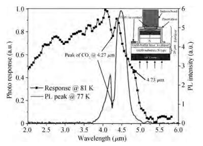
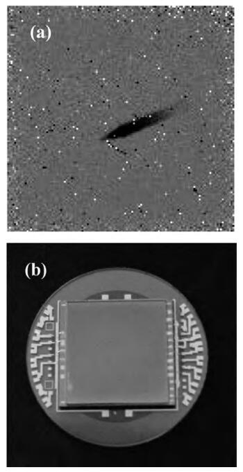
We present the fabrication of a mid-wavelength infrared focal plane array (FPA) based on type-Ⅱ InAs/GaSb strain layer superlattices (SLs). The detectors contain a 400-period 8 ML InAs/8 ML GaSb SL active layer, which is grown by solid source molecular beam epitaxy on GaSb (100) N type substrates. Lattice mismatch between the superlattices and GaSb substrate achieves 148.9 ppm. The full width at half maximum of the first order satellite peak from X-ray diffraction was 28 arcsec. Single element detectors and FPA with a 128×128 pixels were fabricated using citric acid based solution wet chemical etching. Chemical and physical passivation effectively reduces the surface leakage and this process was characterized by Ⅰ-Ⅴ measurement. The devices showed a 50% cut-off wavelength of 4.73 μm at 77 K. The photodiode exhibited an R0A of 103 Ω· cm2. The FPA was characterized with an integration time of 0.5 ms and F/2.0 optics at 77 K and the average blackbody detectivity of the detectors is 2.01×109 cm·Hz1/2/W.

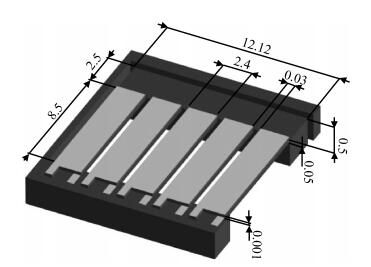
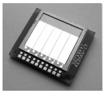
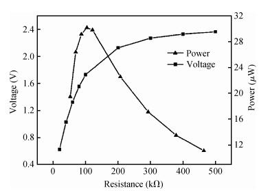
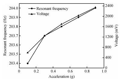
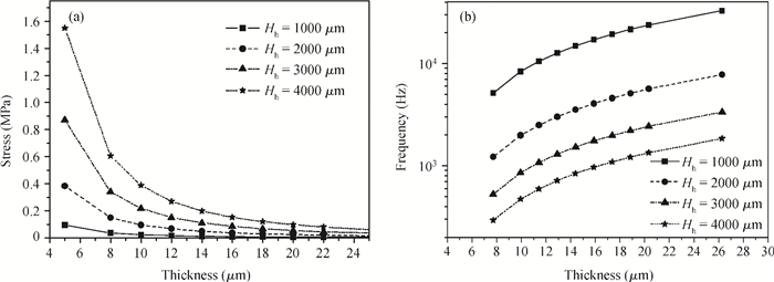
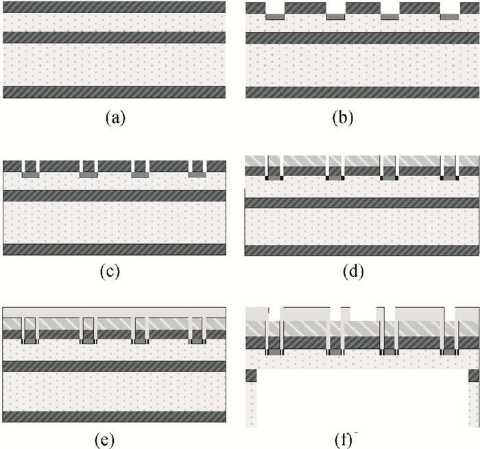
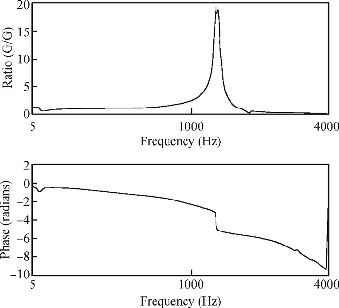
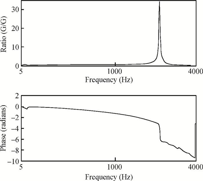
The fabrication and measurement results of the vibration energy harvester arrays based on the piezoelectric aluminum nitride (AlN) film are presented. The structure design and fabrication process of the device are introduced. The key material, the AlN film with crystal orientation (002), was deposited by pulsed-DC magnetron sputtering and characterized by X-ray diffraction (XRD). The resonant frequency, power out, and the open circuit voltage of the device are detected. The optimized load of 80 kΩ and a remarkable maximum power out of 30.4 μW are obtained when the acceleration of 0.9g (g is standard gravity acceleration) is applied.

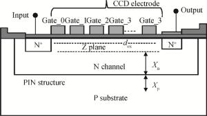
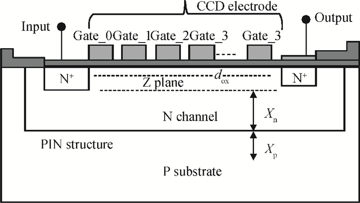
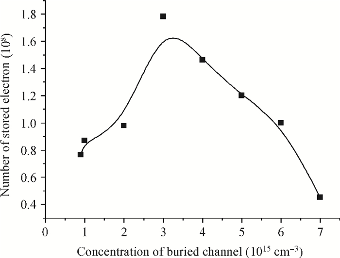
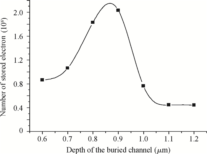
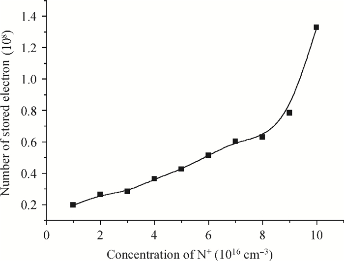
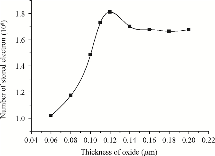
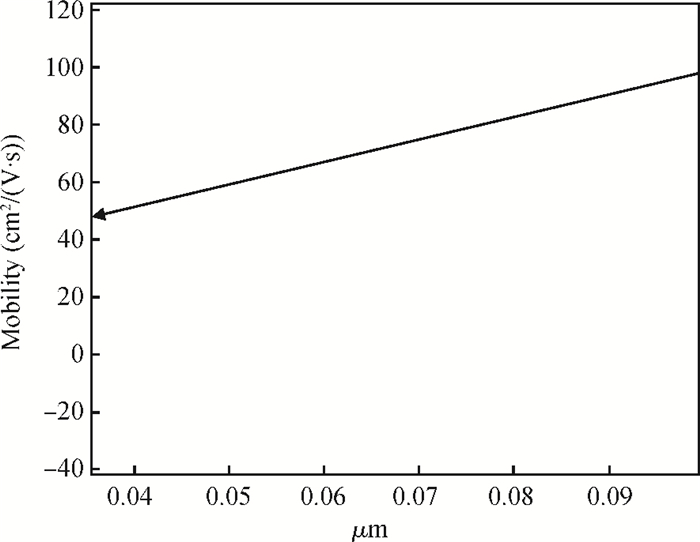
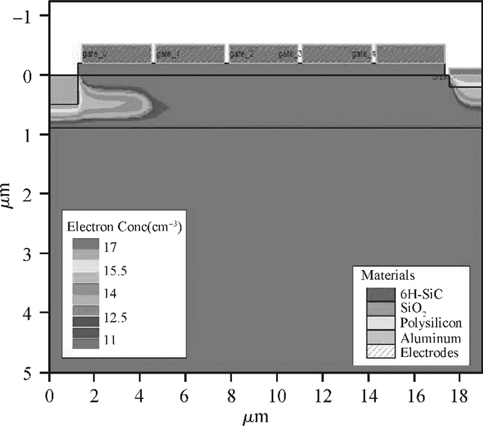
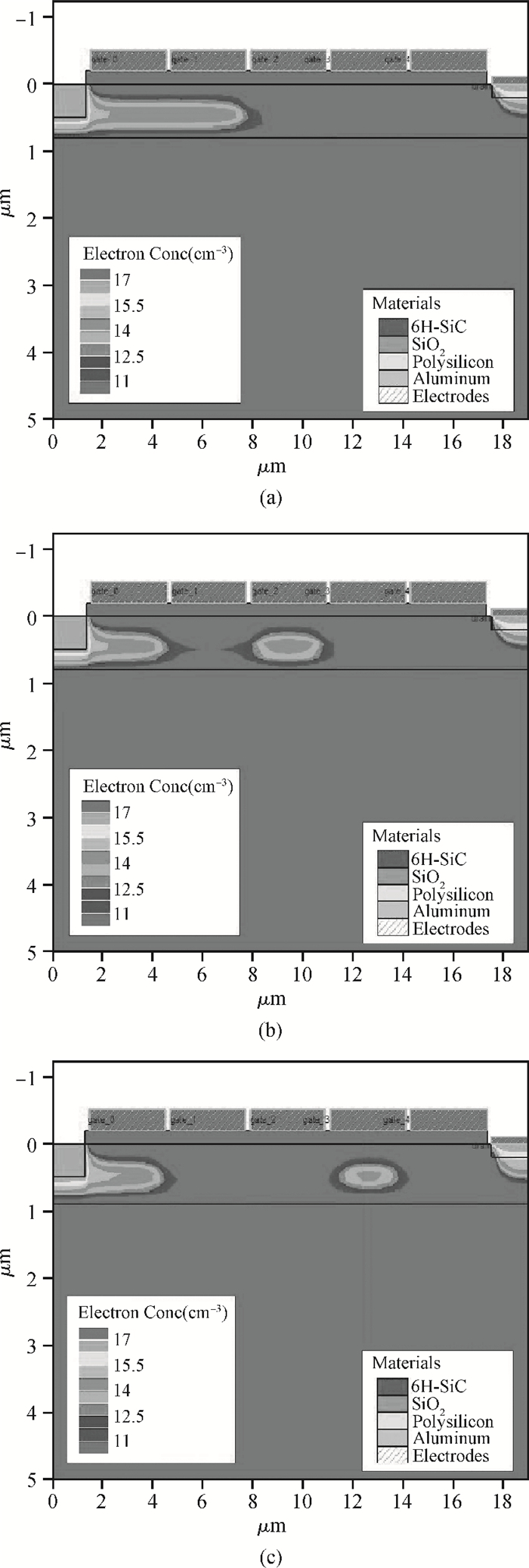
An SiC optoinjected charge-coupled device with buried channels (BCCD) is designed for the detection of ultraviolet light (UV), and its feasibility is studied by means of Silvaco numerical siumlation software. Charge storage and transfer characteristics of the BCCD can be conformed by sitimeslation results. The buried channel design is a key point to realize the high sensitivity of the device. The channel mobility of electrons in the 6H-SiC BCCD can be changed from 47 to 200 cm2/(V· s) when the channel is replaced from surface to the subsurface of 0.2 μm. With the optimized device parameters, the density of stored electrons can reach up to 1.062×1011 cm-2 and the number of stored electrons is up to 1.826×10⁸ for UV light with wavelengths from 200 to 380 nm and an intensity of 0.1 W/cm2 under a driving voltage of 15 V at room temperature.


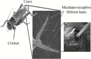
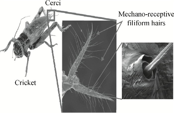
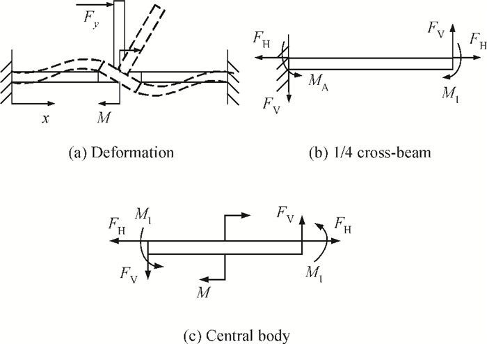
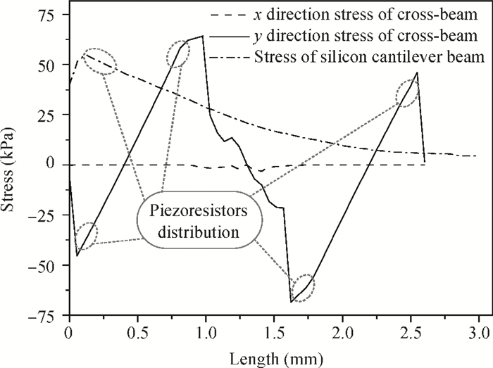
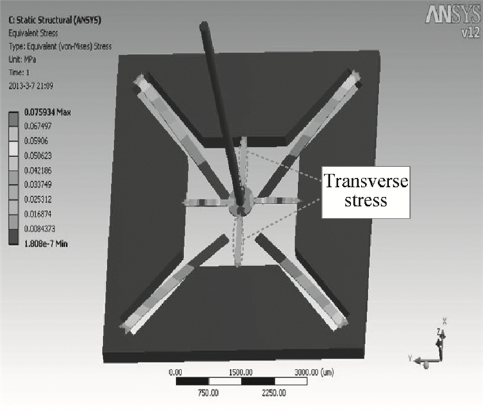
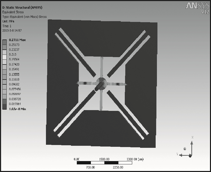
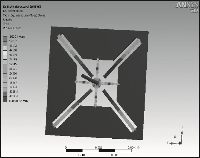
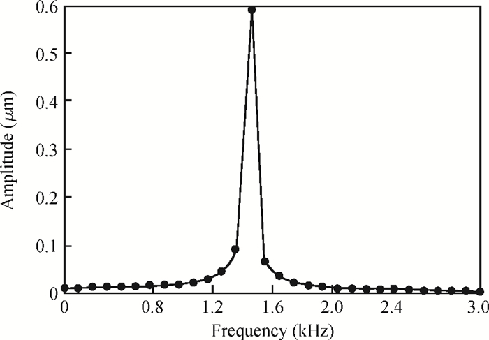
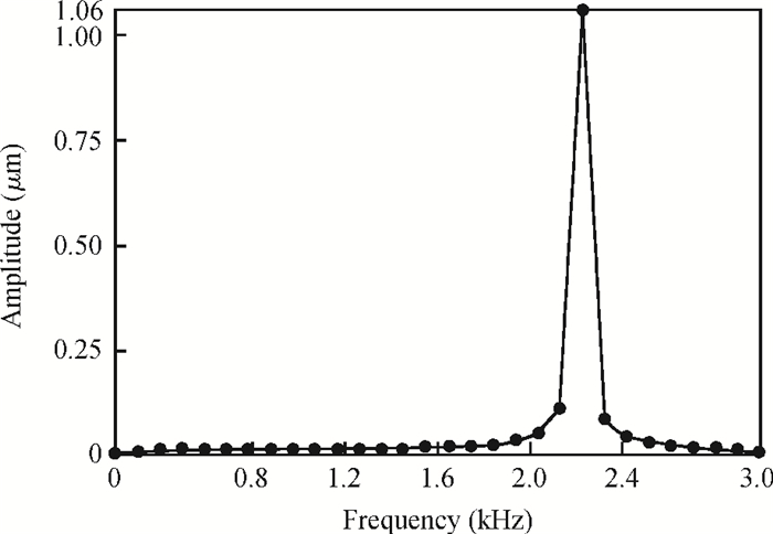
A biomimetic three-dimensional piezoresistive vibration sensor based on MEMS technology is reported. The mechanical properties of the sensor are analyzed and the static and dynamic characteristics of the sensor are simulated by ANSYS Workbench12.0. The structure was made by MEMS processes including lithography, ion implantation, PECVD, etching, etc. Finally, the sensor is tested by using a TV5220 sensor auto calibration system. The results show that the lowest sensitivity of the sensor is 394.7 μ V/g and can reach up to 460.2 μ V/g, and the dimension coupling is less than 0.6152%, and the working frequency range is 0-1000 Hz.


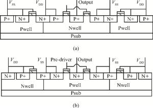
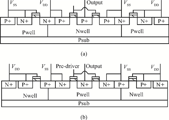
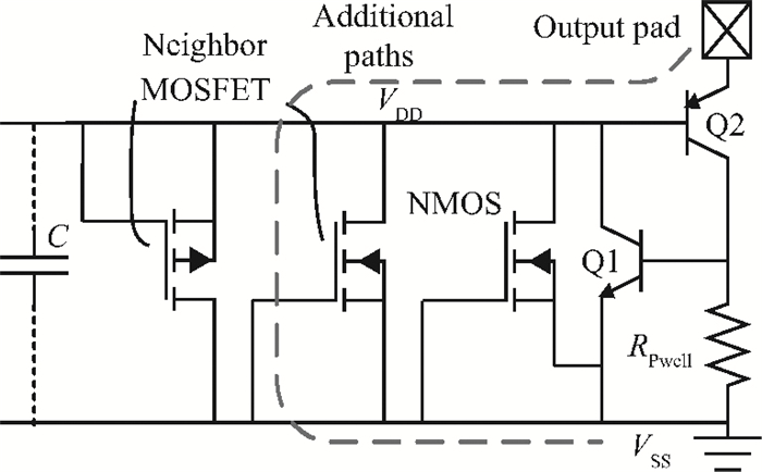
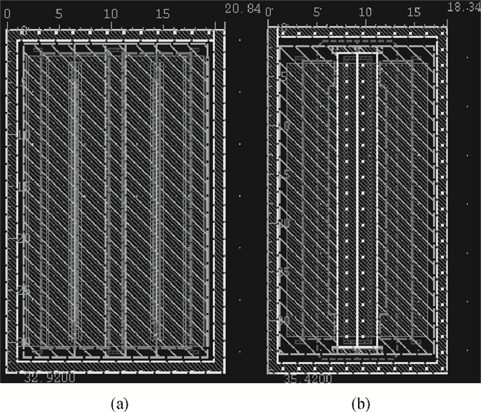
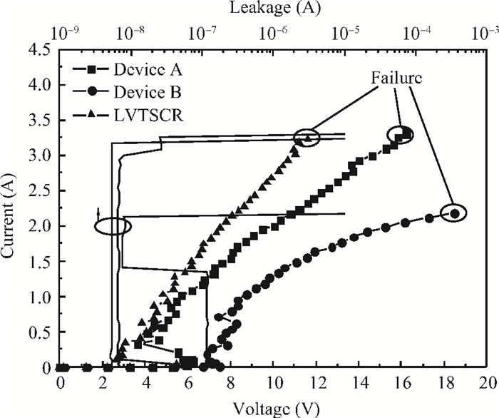
Electro-static discharge (ESD) is always a serious threat to integrated circuits. To achieve higher robustness and a smaller die area at the same time, a novel protection structure for the output pad is proposed. The complementary SCR devices in this structure can protect not only the output under positive or negative stresses versus VDD or VSS, respectively, but also the power rails at the cost of almost no extra area. The robustness of the proposed structure is about three times higher than the conventional four-finger GGNMOS/GDPMOS structure in the same area condition.


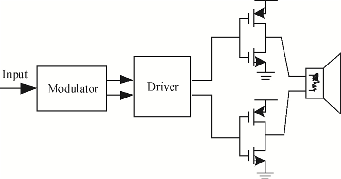
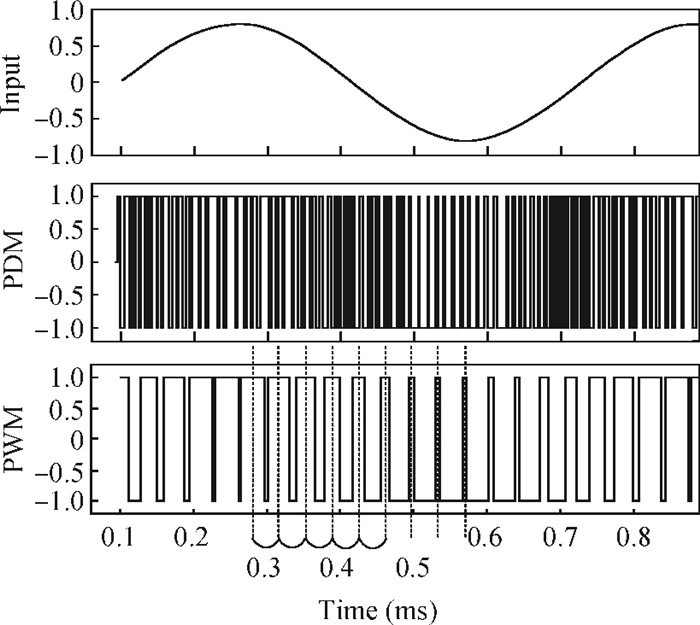
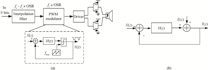
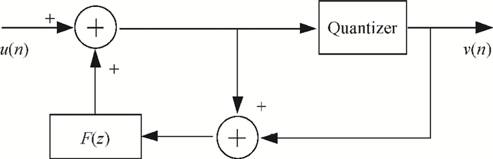
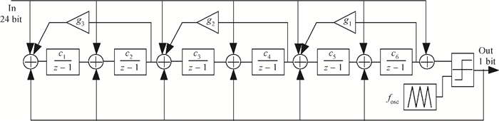
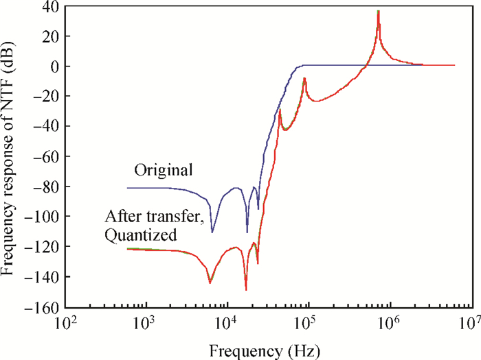
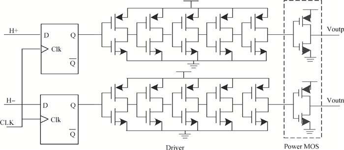
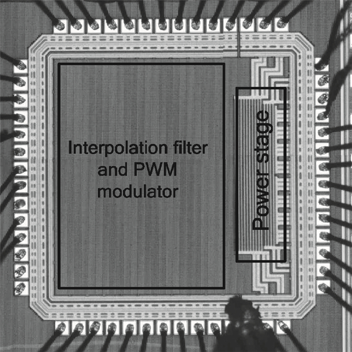
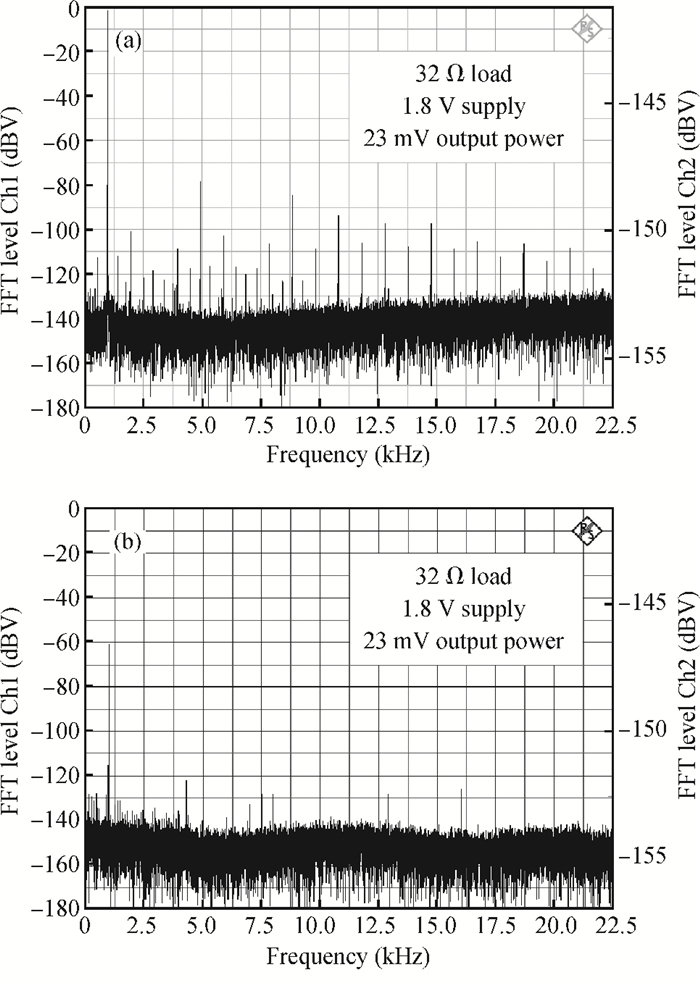
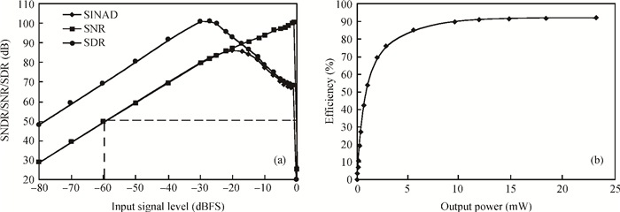
A digital input class-D audio amplifier with a sixth-order pulse-width modulation (PWM) modulator is presented. This modulator moves the PWM generator into the closed sigma-delta modulator loop. The noise and distortions generated at the PWM generator module are suppressed by the high gain of the forward loop of the sigma-delta modulator. Therefore, at the output of the modulator, a very clean PWM signal is acquired for driving the power stage of the class-D amplifier. A sixth-order modulator is designed to balance the performance and the system clock speed. Fabricated in standard 0.18 μm CMOS technology, this class-D amplifier achieves 110 dB dynamic range, 100 dB signal-to-noise rate, and 0.0056% total harmonic distortion plus noise.


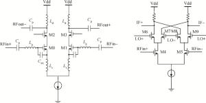
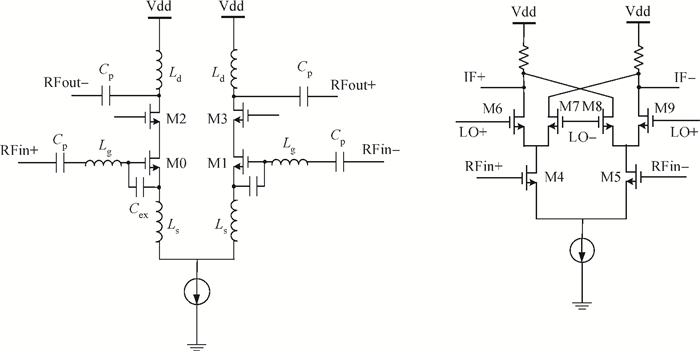
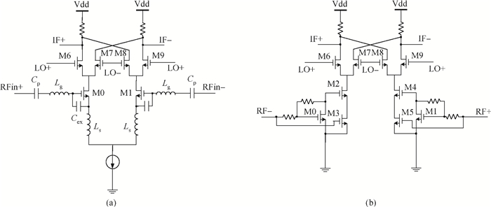
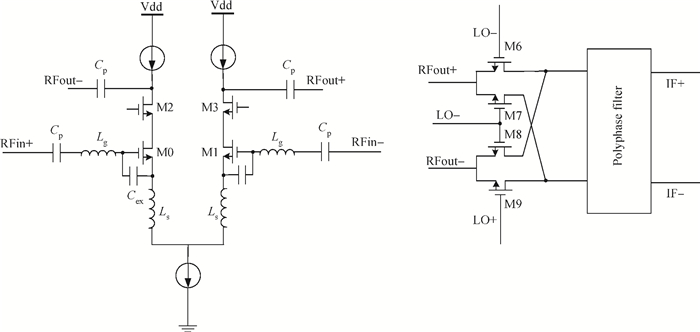
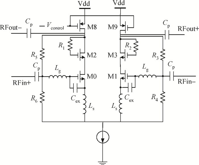
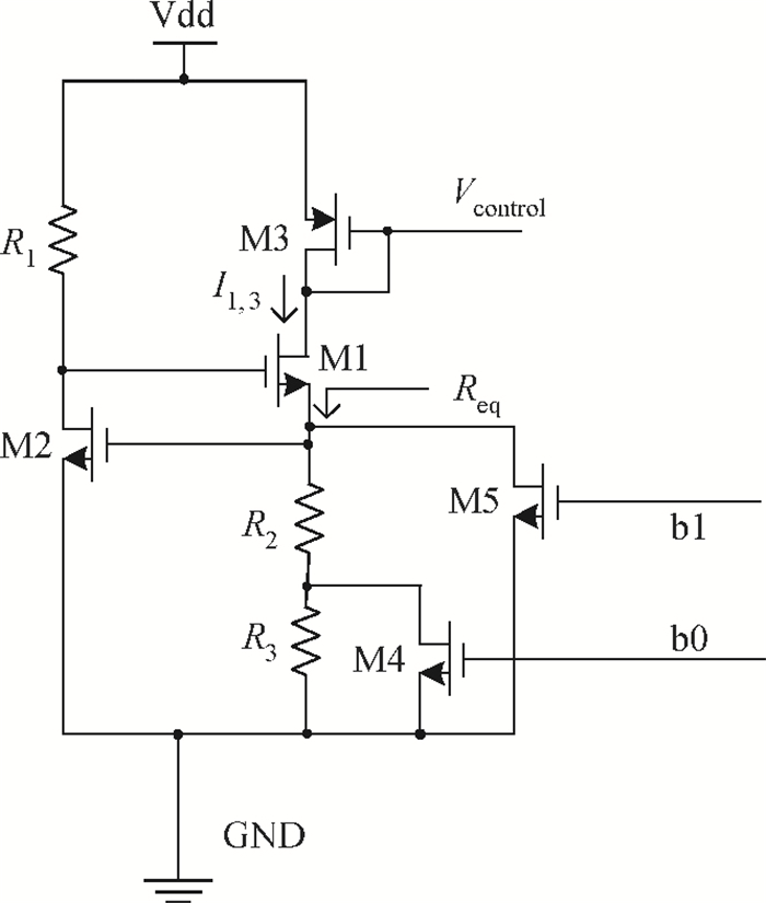
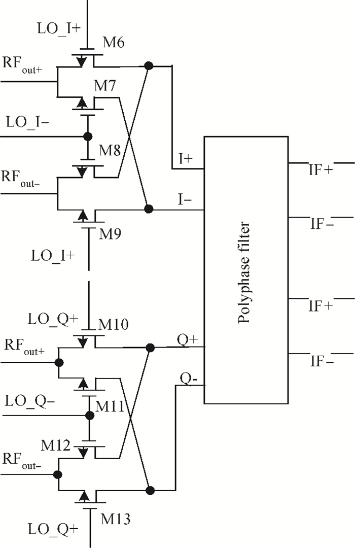
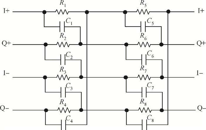
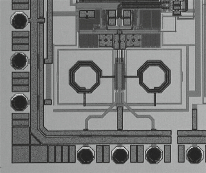
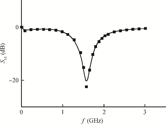
A low power high gain gain-controlled LNA + mixer for GNSS receivers is reported. The high gain LNA is realized with a current source load. Its gain-controlled ability is achieved using a programmable bias circuit. Taking advantage of the high gain LNA, a high noise figure passive mixer is adopted. With the passive mixer, low power consumption and high voltage gain of the LNA + mixer are achieved. To fully investigate the performance of this circuit, comparisons between a conventional LNA + mixer, a previous low power LNA + mixer, and the proposed LNA + mixer are presented. The circuit is implemented in 0.18 μm mixed-signal CMOS technology. A 3.8 dB noise figure, an overall 45 dB converge gain and a 10 dB controlled gain range of the two stages are measured. The chip occupies 0.24 mm2 and consumes 2 mA current under 1.8 V supply.


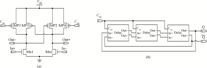
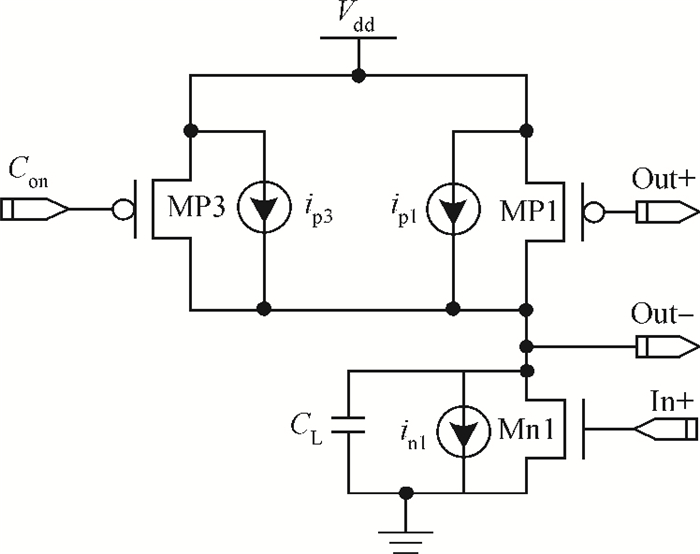
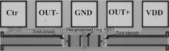
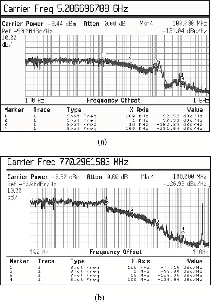
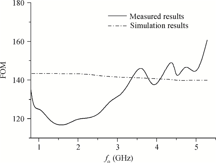
This paper describes a large tuning range low phase noise voltage-controlled ring oscillator (ring VCO) based on a different cascade voltage logic delay cell with current-source load to change the current of output node. The method for optimization is presented. Furthermore, the analysis of performance of the proposed ring VCO is confirmed by the measurement results. The three-stage proposed ring VCO was fabricated in the 180-nm CMOS process of SMIC. The measurement results show that the oscillator frequency of the ring VCO is from 0.770 to 5.286 GHz and the phase noise is 97.93 dBc/Hz at an offset of 1 MHz from 5.268 GHz with a total power of 15.1 mW from a 1.8 V supply while occupying only 0.00175 mm2 of the core die area.


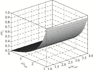
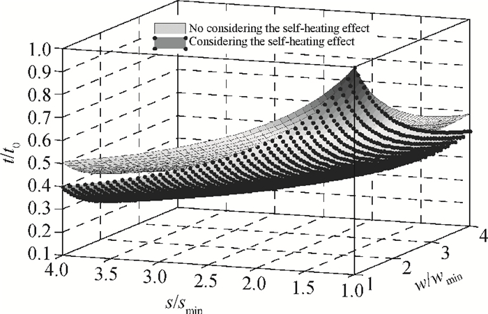
Considering the self-heating effect, an accurate expression for the global interconnection resistance per unit length in terms of interconnection wire width and spacing is presented. Based on the proposed resistance model and according to the trade-off theory, a novel optimization analytical model of delay, power dissipation and bandwidth is derived. The proposed optimal model is verified and compared based on 90 nm, 65 nm and 40 nm CMOS technologies. It can be found that more optimum results can be easily obtained by the proposed model. This optimization model is more accurate and realistic than the conventional optimization models, and can be integrated into the global interconnection design of nano-scale integrated circuits.


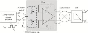
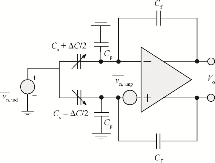
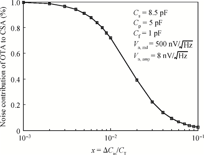
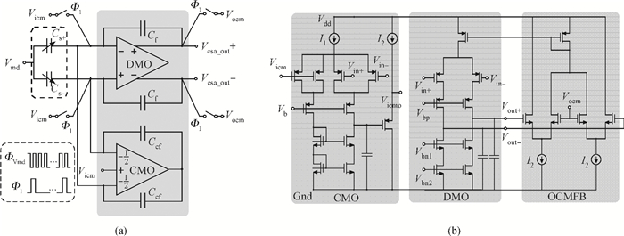
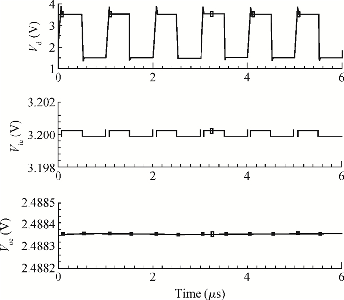
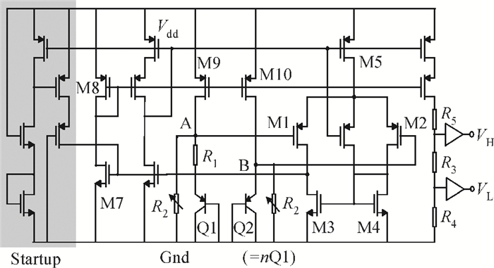
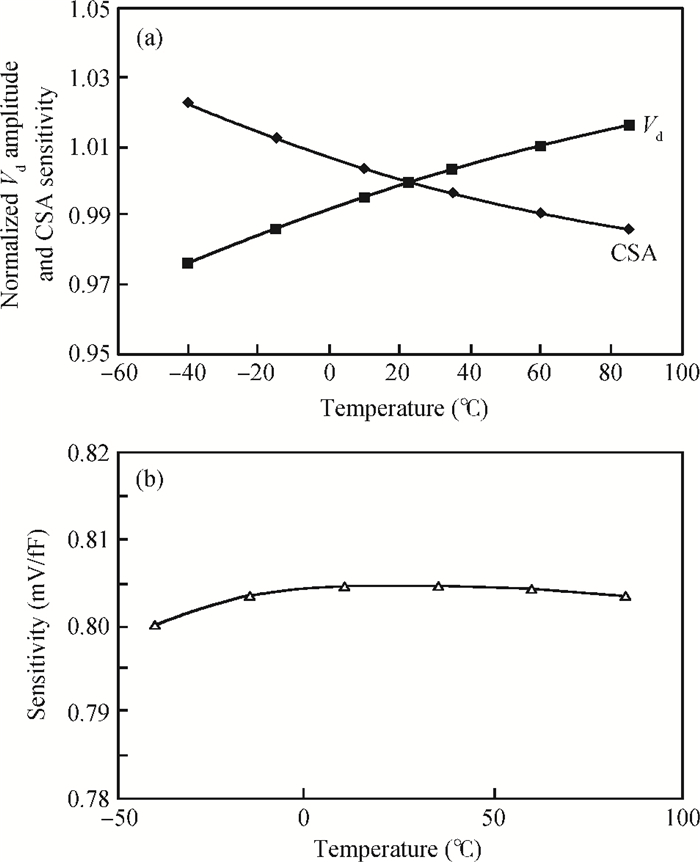
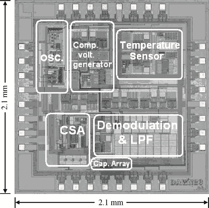
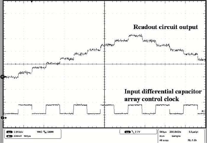
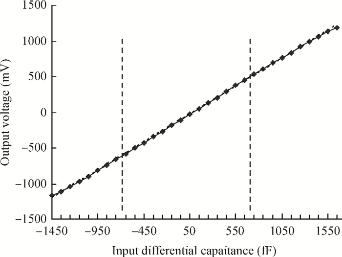
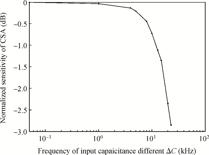
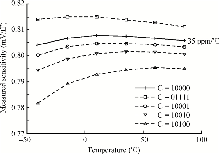
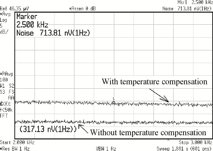
This paper presents a charge-sensitive-amplifier (CSA) based readout circuit for capacitive micro-electro-mechanical-system (MEMS) sensors. A continuous-time (CT) readout structure using the chopper technique is adopted to cancel the low frequency noise and improve the resolution of the readout circuits. An operational trans-conductance amplifier (OTA) structure with an auxiliary common-mode-feedback-OTA is proposed in the fully differential CSA to suppress the chopper modulation induced disturbance at the OTA input terminal. An analog temperature compensation method is proposed, which adjusts the chopper signal amplitude with temperature variation to compensate the temperature drift of the CSA readout sensitivity. The chip is designed and implemented in a 0.35 μm CMOS process and is 2.1×2.1 mm2 in area. The measurement shows that the readout circuit achieves 0.9 aF/$\sqrt {{\rm{Hz}}}$ capacitive resolution, 97 dB dynamic range in 100 Hz signal bandwidth, and 0.8 mV/fF sensitivity with a temperature drift of 35 ppm/℃ after optimized compensation.


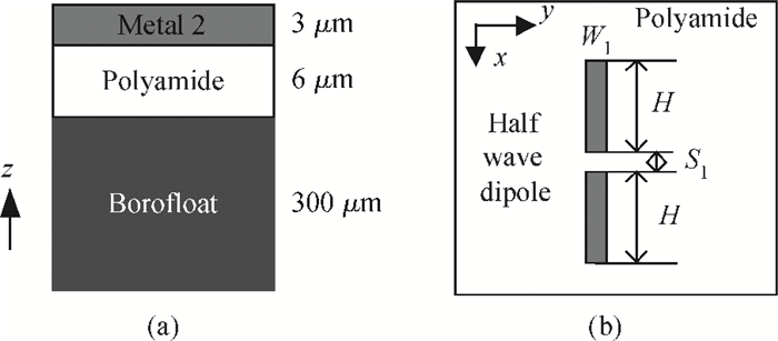
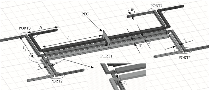
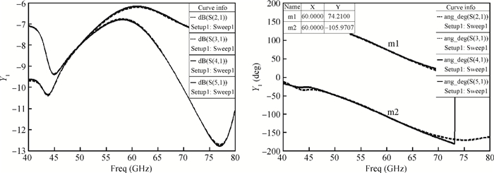
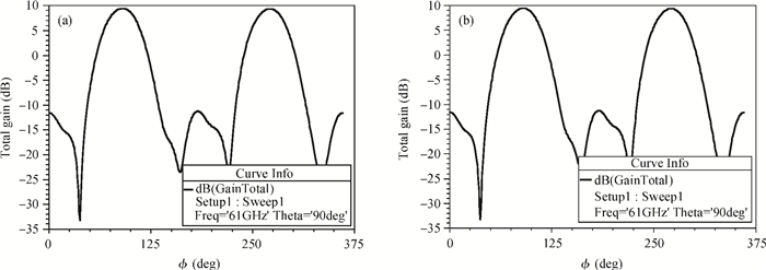
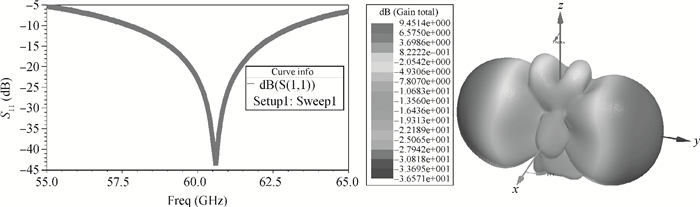
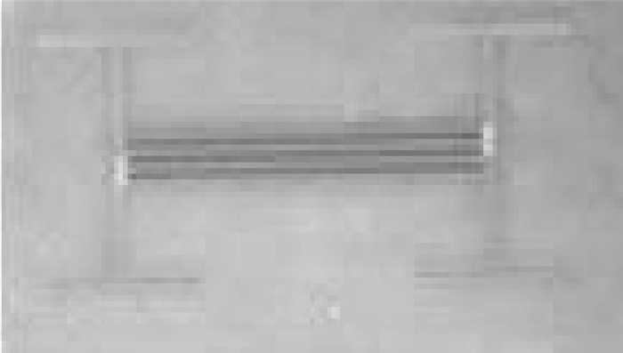
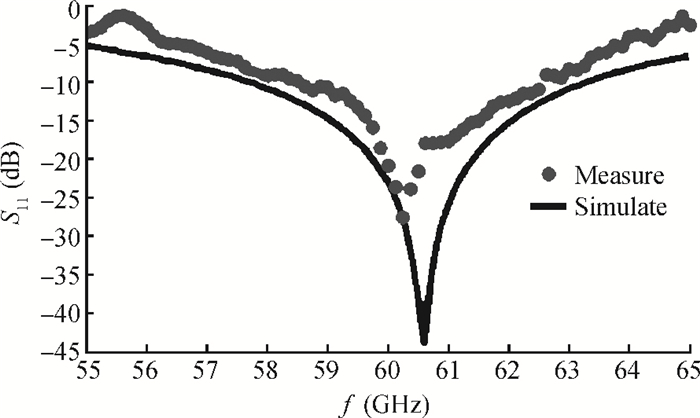
This design is presented of a 2X2 planar array, with a half-wave dipole antenna to be its element, on a new substrate material, Schott Borofloat, with CMOS technology in the 60 GHz band. In the proposed structure, all the designs are based on the CMOS technology and similar performance could be achieved with the same size in contrast to the design on low-temperature co-fired ceramic (LTCC). This could lead to the improving of the compatibility with the CMOS IC process, the design cost and the design precision which is restricted in the LTCC process. The simulated -10 dB bandwidth of the array is from 58 to 64 GHz. A peak gain of 9.4 dBi is achieved. Good agreement on return loss is achieved between simulations and measurements.

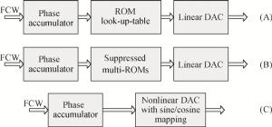
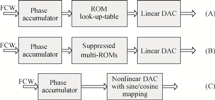
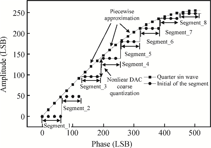
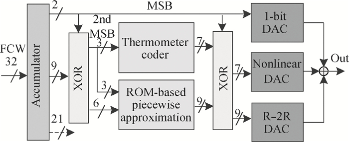
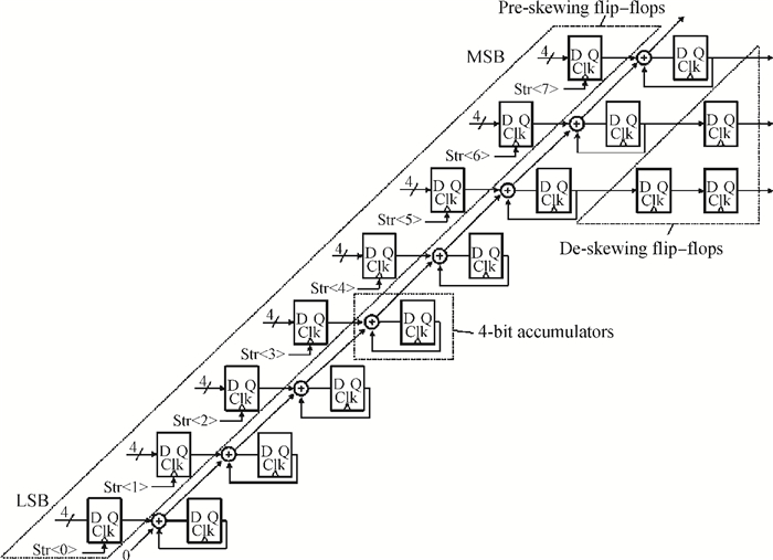
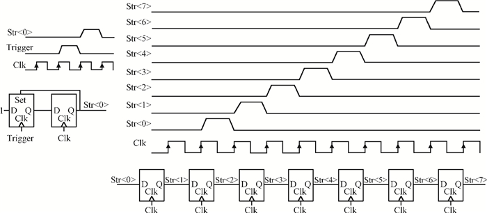
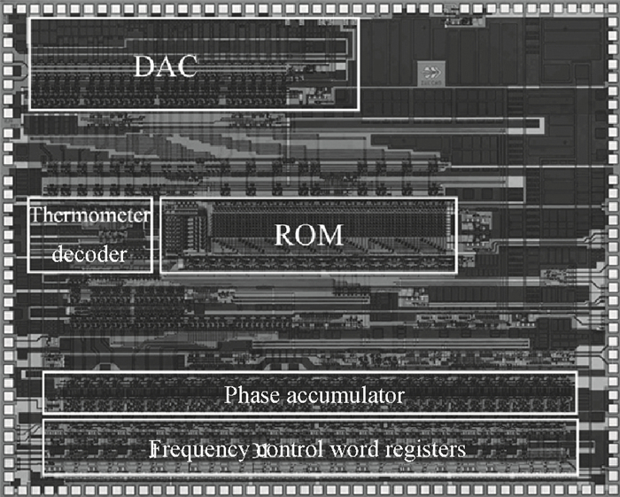
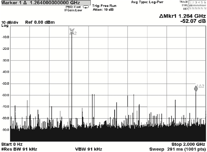
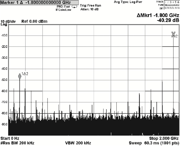
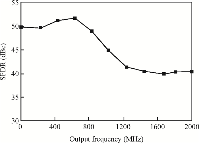
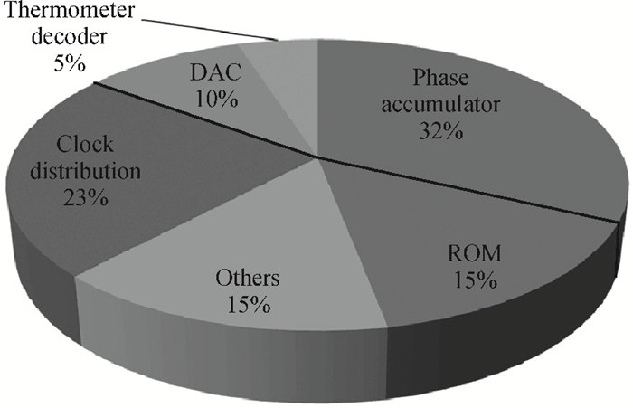
This paper presents a novel direct digital frequency synthesizer (DDFS) architecture based on nonlinear DAC coarse quantization and the ROM-based piecewise approximation method, which has the advantages of high speed, low power and low hardware resources. By subdividing the sinusoid into a collection of phase segments, the same initial value of each segment is realized by a nonlinear DAC. The ROM is decomposed with a coarse ROM and fine ROM using the piecewise approximation method. Then, the coarse ROM stores the offsets between the initial value of the common segment and the initial value of each line in the same segment. Meanwhile, the fine ROM stores the differences between the line values and the initial value of each line. A ROM compression ratio of 32 can be achieved in the case of 11 bit phase and 9 bit amplitude. Based on the above method, a prototype chip was fabricated using 1.4 μm GaAs HBT technology. The measurement shows an average spurious-free dynamic range (SFDR) of 45 dBc, with the worst SFDR only 40.07 dBc at a 4.0 GHz clock. The chip area is 4.6×3.7 mm2 and it consumes 7 W from a -4.9 V power supply.