Based on first-principle calculations, the electronic structures and optical properties of a single-walled (7, 0) SiC nanotube (SiCNT) with a carbon vacancy defect or a silicon vacancy defect are investigated. In the three silicon atoms around the carbon vacancy, two atoms form a stable bond and the other is a dangling bond. A similar structure is found in the nanotube with a silicon vacancy. A carbon vacancy results in a defect level near the top of the valence band, while a silicon vacancy leads to the formation of three defect levels in the band gap of the nanotube. Transitions between defect levels and energy levels near the bottom of the conduction band have a close relationship with the formation of the novel dielectric peaks in the lower energy range of the dielectric function.


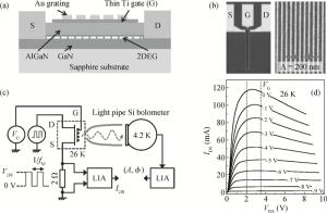
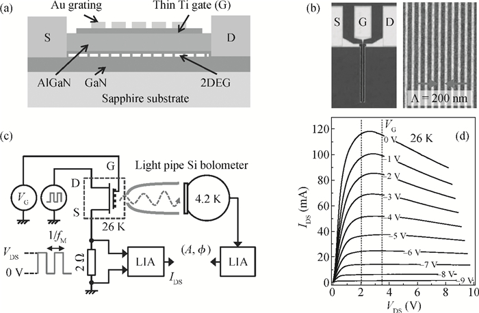
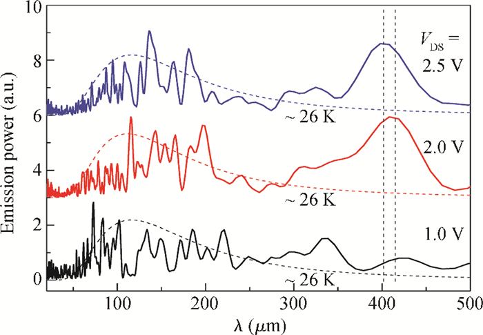
In a grating-coupled high-electron-mobility transistor, weak terahertz emission with wavelength around 400 μm was observed by using a Fourier-transform spectrometer. The absolute terahertz emission power was extracted from a strong background blackbody emission by using a modulation technique. The power of terahertz emission is proportional to the drain-source current, while the power of blackbody emission has a distinct relation with the electrical power. The dependence on the drain-source bias and the gate voltage suggests that the terahertz emission is induced by accelerated electrons interacting with the grating.


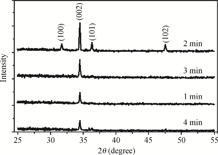
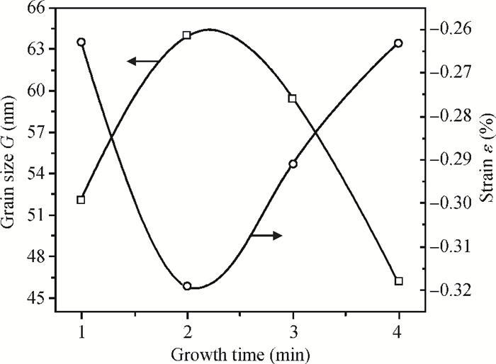
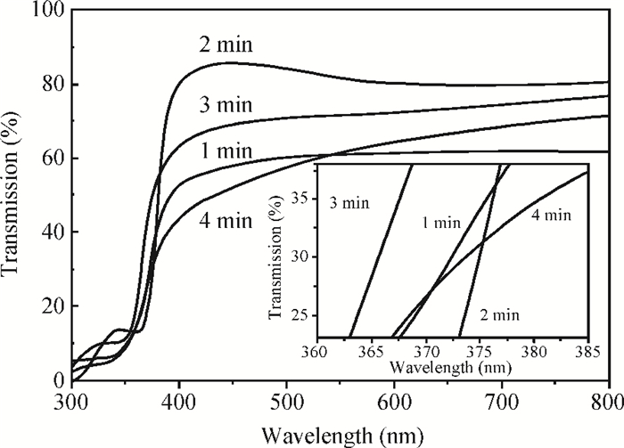
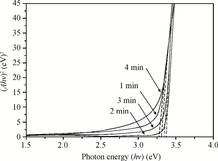
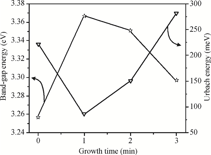
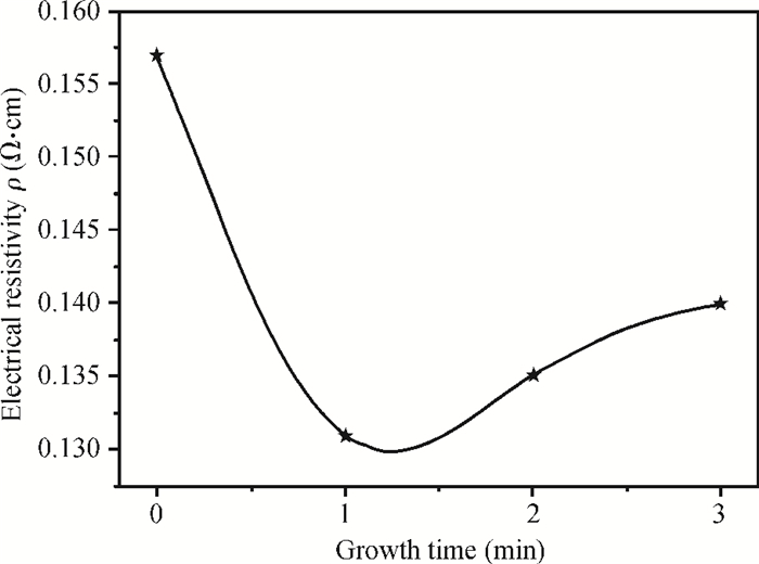
This paper examines the growth of ZnO thin films on glass substrate at 350℃ using an ultrasonic spray technique. We have investigated the influence of growth time ranging from 1 to 4 min on structural, optical and electrical properties of ZnO thin films. The as-grown films exhibit a hexagonal structure wurtzite and are (002) oriented. The maximum value of grain size G=63.99 nm is attained for ZnO films grown at 2 min. The average transmittance is about 80%, thus the films are transparent in the visible region. The optical gap energy is found to increase from 3.26 to 3.37 eV with growth time increased from 1 to 2 min. The minimum value of electrical resistivity of the films is 0.13 Ω·cm obtained at 2 min. A systematic study on the influence of growth time on the properties of ZnO thin films deposited by ultrasonic spray at 350℃ has been reported.
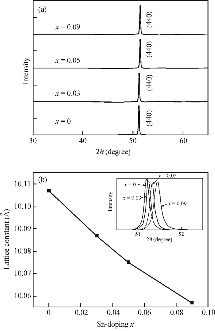
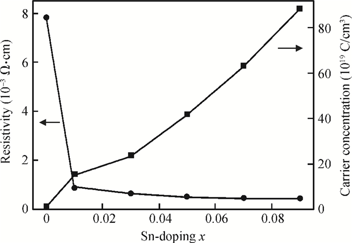
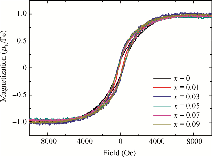
Room-temperature ferromagnetism was observed in (In0.95-xSnxFe0.05)2O3 (x=0-0.09) films deposited by pulsed laser deposition. XRD results give a direct proof that both Sn and Fe ions have been incorporated into the In2O3 lattice. The carrier concentration in the films is obviously increased by the Sn-doping, while the ferromagnetic properties are rarely changed. We think that in our Fe-doped In2O3 films, the oxygen vacancy-related bound magnetic polaron model, rather than the carrier-mediated RKKY coupling, is the main mechanism for the observed ferromagnetism.
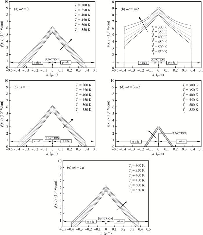
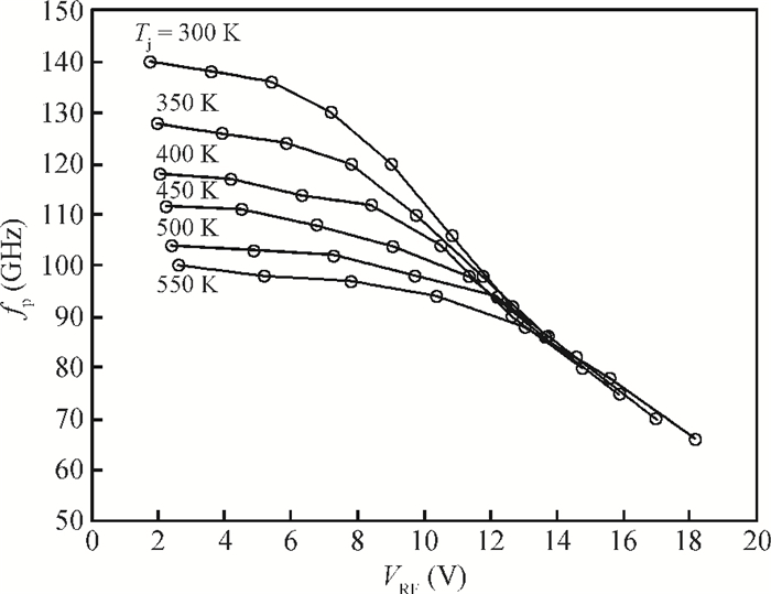
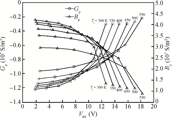
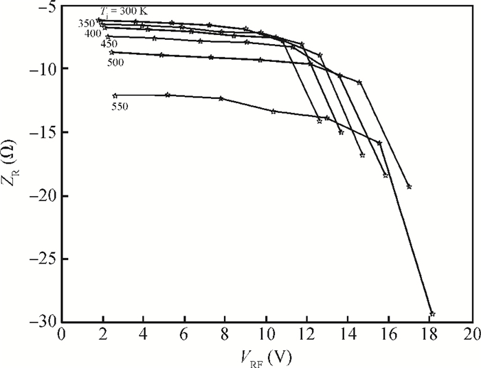
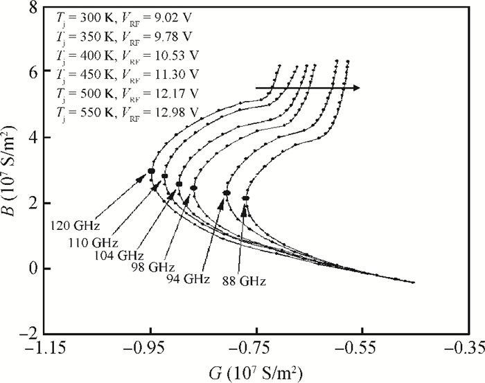
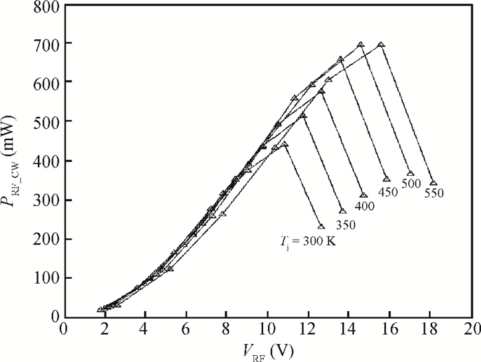
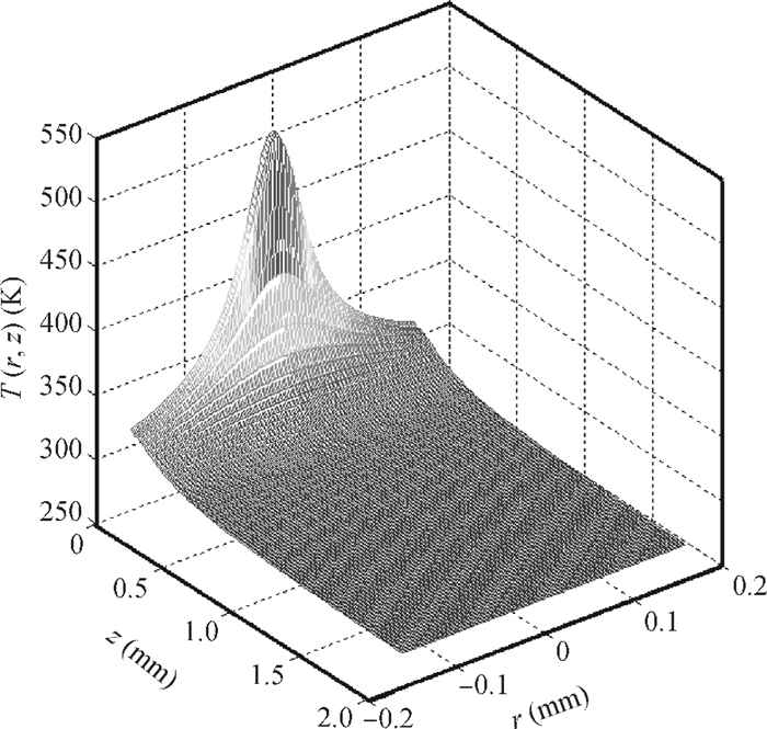
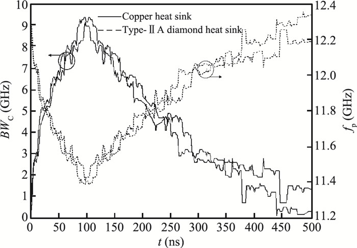
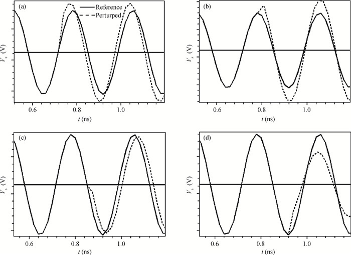
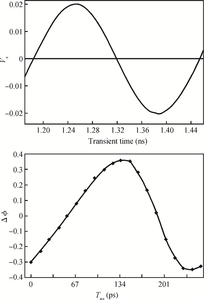
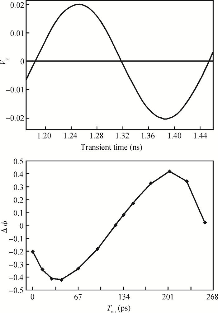
The authors have developed a large-signal simulation technique extending an in-house small-signal simulation code for analyzing a 94 GHz double-drift region impact avalanche transit time device based on silicon with a non-sinusoidal voltage excitation and studied the effect of junction temperature between 300 and 550 K on the large-signal characteristics of the device for both continuous wave (CW) and pulsed modes of operation. Results show that the large-signal RF power output of the device in both CW and pulsed modes increases with the increase of voltage modulation factor up to 60%, but decreases sharply with further increase of voltage modulation factor for a particular junction temperature; while the same parameter increases with the increase of junction temperature for a particular voltage modulation factor. Heat sinks made of copper and type-ⅡA diamond are designed to carry out the steady-state and transient thermal analysis of the device operating in CW and pulsed modes respectively. Authors have adopted Olson's method to carry out the transient analysis of the device, which clearly establishes the superiority of type-ⅡA diamond over copper as the heat sink material of the device from the standpoint of the undesirable effect of frequency chirping due to thermal transients in the pulsed mode.


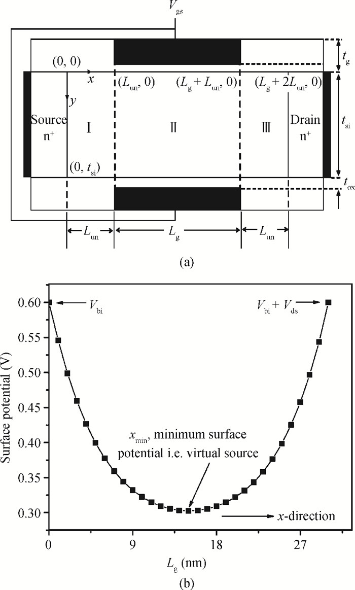
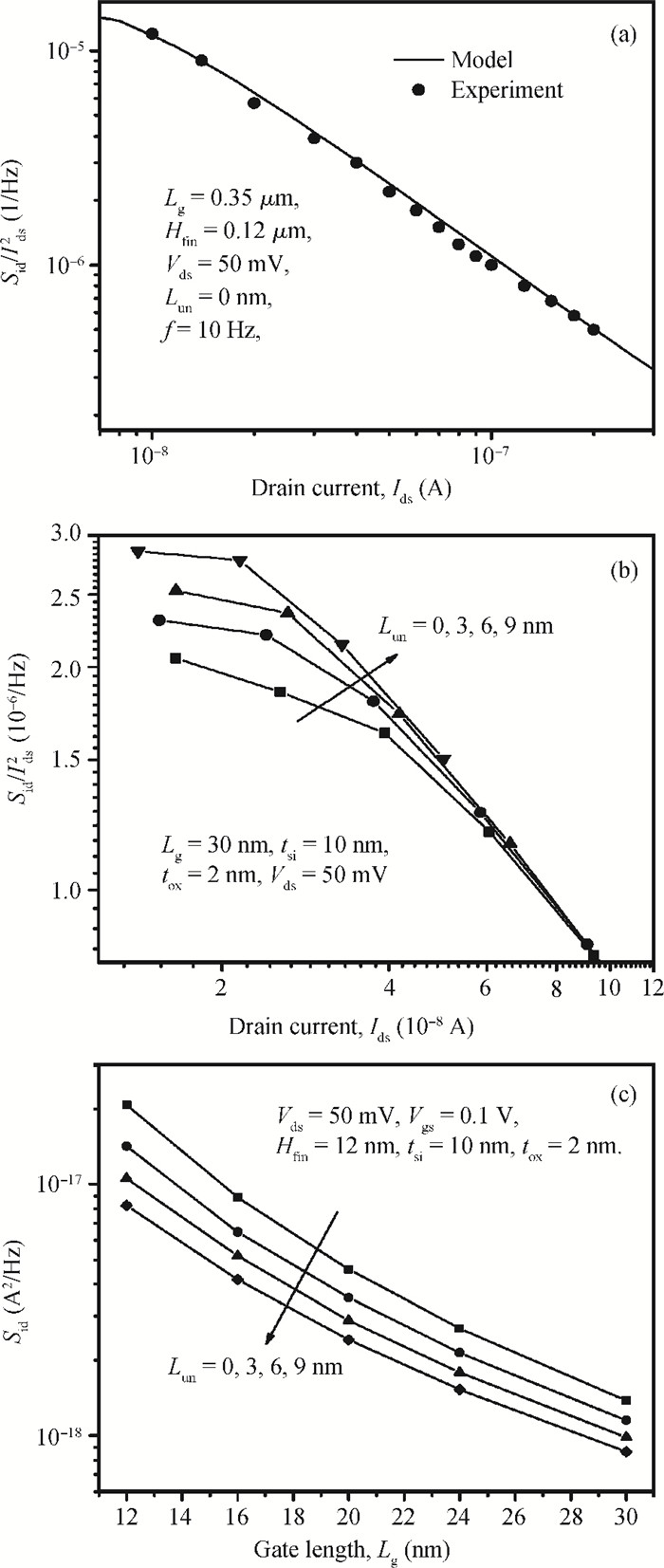
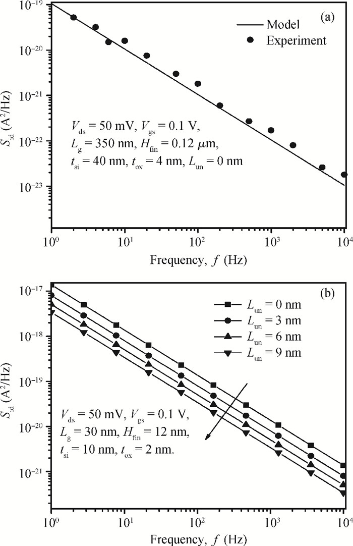
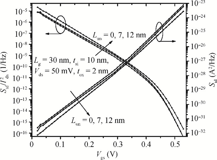
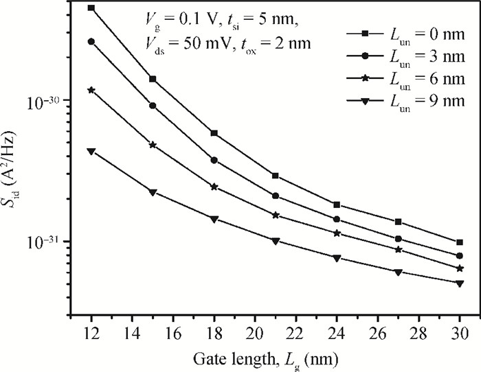
We propose an analytical model for drain current and inversion charge in the subthreshold region for an underlap DG FinFET by using the minimum channel potential method, i.e., the virtual source. The flicker and thermal noise spectral density models are also developed using these charge and current models expression. The model is validated with already published experimental results of flicker noise for DG FinFETs. For an ultrathin body, the degradation of effective mobility and variation of the scattering parameter are considered. The effect of device parameters like gate length Lg and underlap length Lun on both flicker and thermal noise spectral densities are also analyzed. Increasing Lg and Lun, increases the effective gate length, which reduces drain current, resulting in decreased flicker and thermal noise density. A decrease of flicker noise is observed for an increase of frequency, which indicates that the device can be used for wide range of frequency applications.


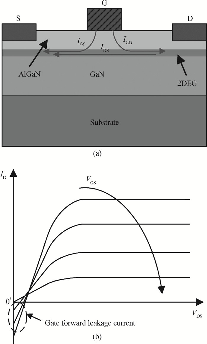
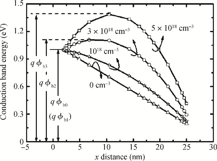
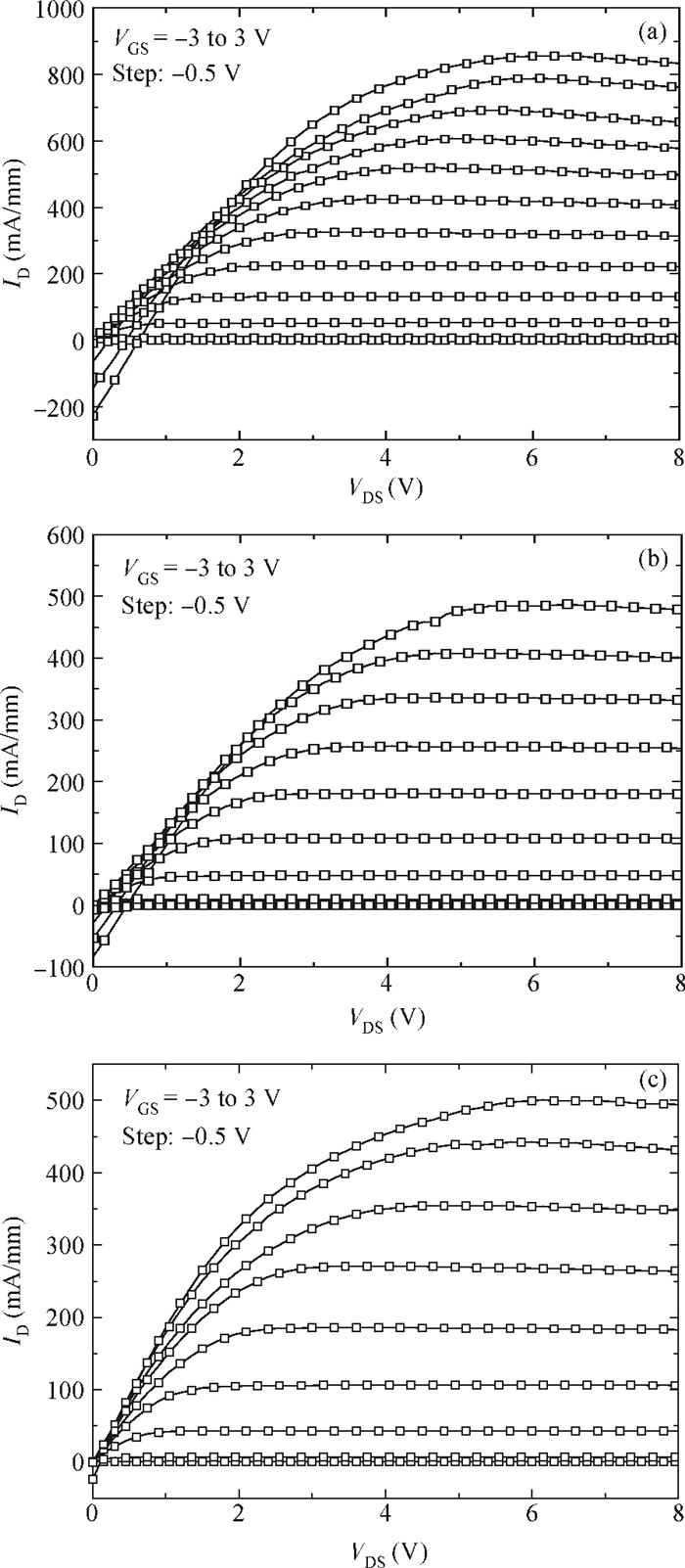
The gate forward leakage current in AlGaN/GaN high electron mobility transistors (HEMTs) is investigated. It is shown that the current which originated from the forward biased Schottky-gate contributed to the gate forward leakage current. Therefore, a fluorine-plasma surface treatment is presented to induce the negative ions into the AlGaN layer which results in a higher metal-semiconductor barrier. Consequently, the gate forward leakage current shrinks. Experimental results confirm that the gate forward leakage current is decreased by one order magnitude lower than that of HEMT device without plasma treatment. In addition, the DC characteristics of the HEMT device with plasma treatment have been studied.


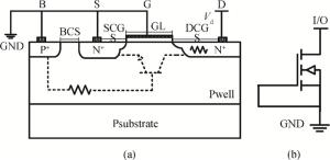
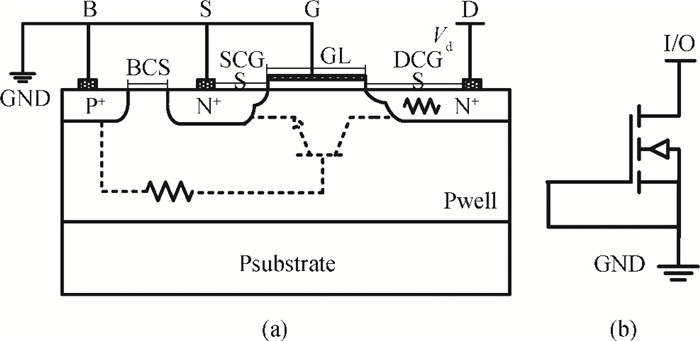
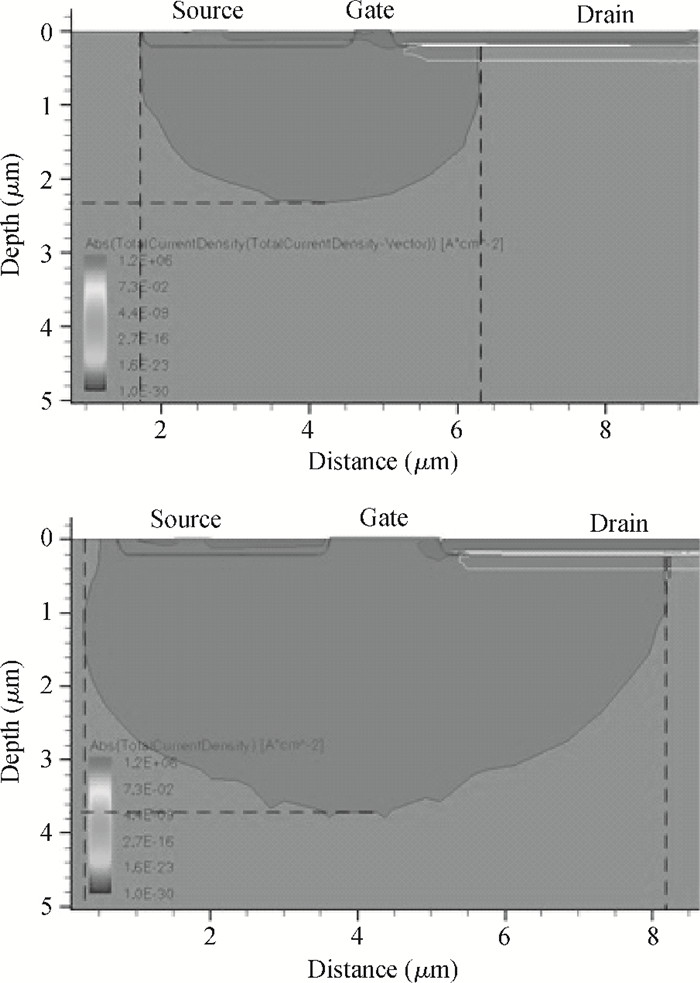
Contrary to general understanding, a test result shows that devices with a shorter channel length have a degraded ESD performance in the advanced silicided CMOS process. Such a phenomenon in a gate-grounded NMOSFET (GGNMOS) was investigated, and the current spreading effect was verified as the predominant factor. Due to transmission line pulse (TLP) measurements and Sentaurus technology computer aided design (TCAD) 2-D numerical simulations, parameters such as current gain, on-resistance and power density were discussed in detail.


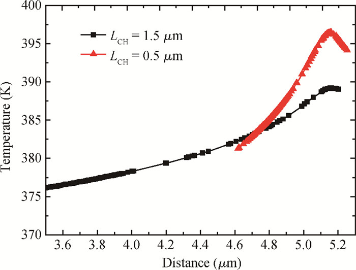

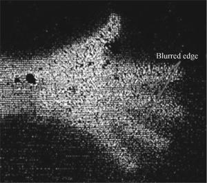
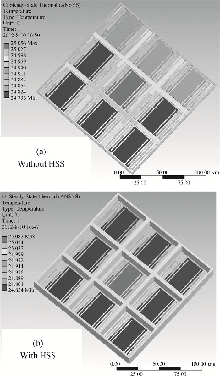
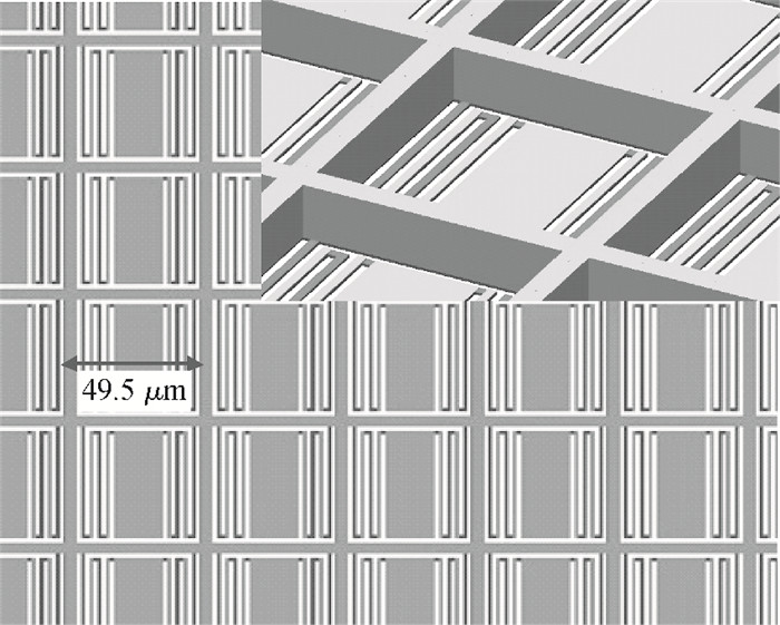
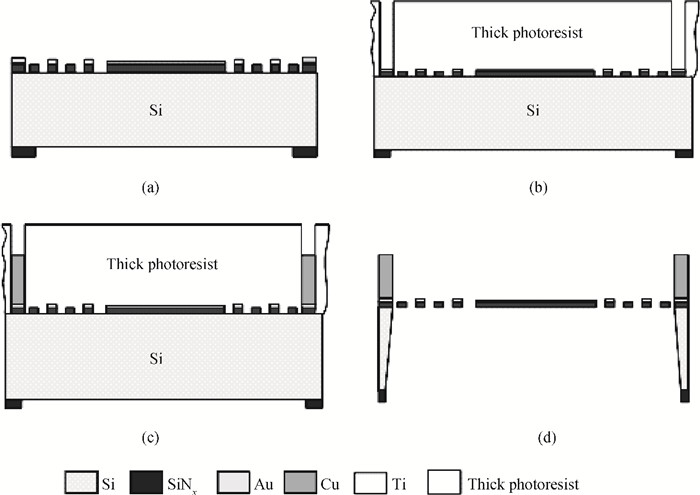
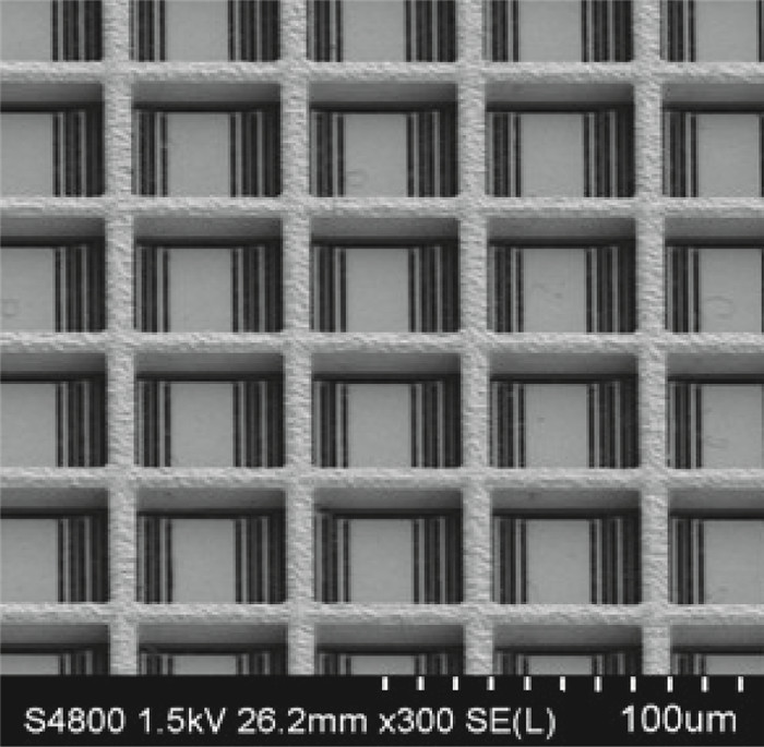
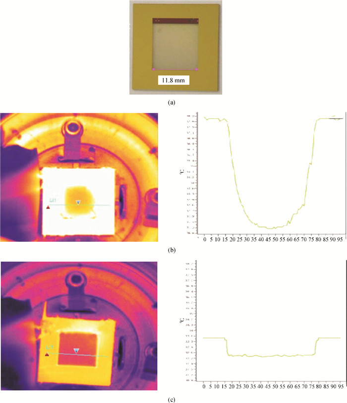
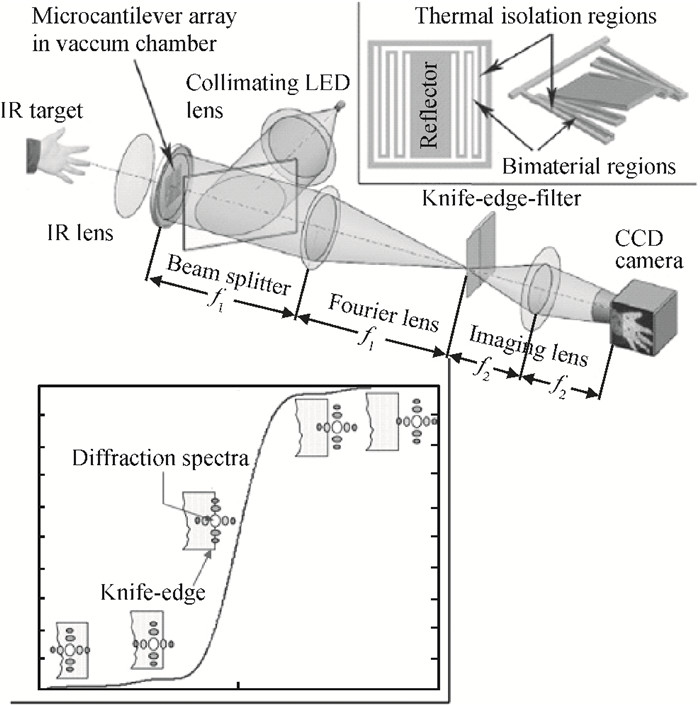
A substrate-free optical readout focal plane array (FPA) operating in 8-12 μm with a heat sink structure (HSS) was fabricated and its performance was tested. The temperature distribution of the FPA with an HSS investigated by using a commercial FLIR IR camera shows excellent uniformity. The thermal cross-talk effect existing in traditional substrate-free FPAs was eliminated effectively. The heat sink is fabricated successfully by electroplating copper, which provides high thermal capacity and high thermal conductivity, on the frame of substrate-free FPA. The FPA was tested in the optical-readout system, the results show that the response and NETD are 13.6 grey/K (F/#=0.8) and 588 mK, respectively.

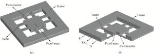
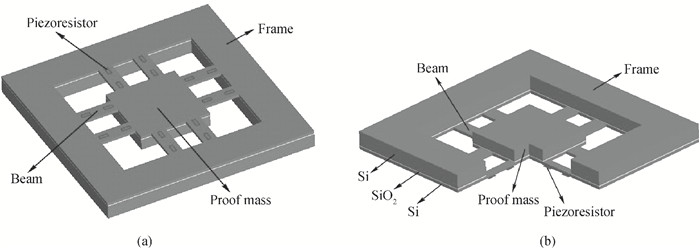
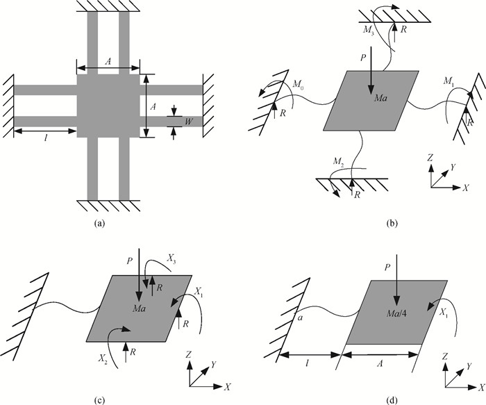
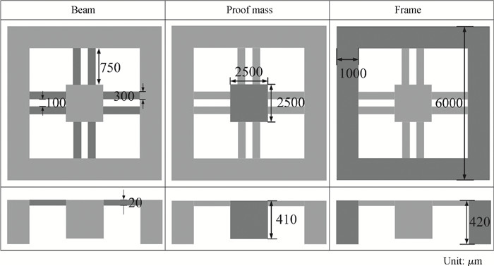
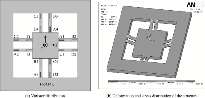
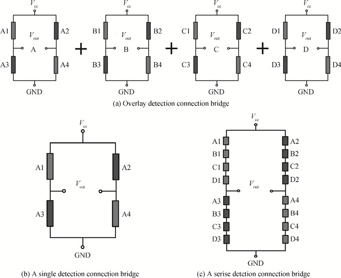
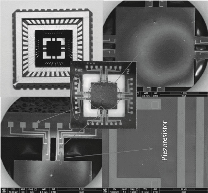
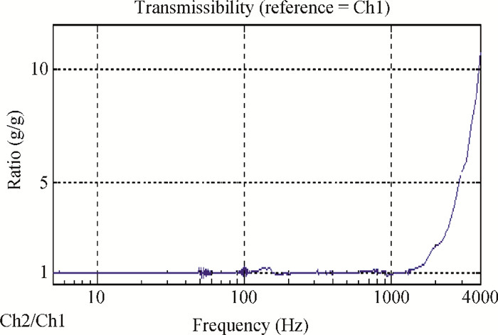
This paper describes the design, simulation, processing and test result of a high sensitivity accelerometer based on the piezoresistive effect which uses an overlay bridge detection method. The structure of this accelerometer is supersymmetric "mass-beams". This accelerometer has 8 beams, where two varistors are put in the two ends. Four varistors compose a Wheatstone bridge and the output voltages of the 4 Wheatstone bridges have been superimposed as the final output voltage. The sensitivity of the accelerometer can be improved effectively by these clever methods. A simplified mathematical model has been created to analyze the mechanical properties of the sensor, then the finite element modeling and simulation have been used to verify the feasibility of the accelerometer. The results show that the sensitivity of the accelerometer is 1.1381 mV/g, which is about four times larger than that of the single bridge accelerometers and series bridge sensor. The bandwidth is 0-1000 Hz which is equal to that of the single bridge accelerometers and the series bridge sensor. The comparison reveals that the new overlay detection bridge method can improve the sensitivity of the sensor in the same bandwidth. Meanwhile, this method provides an effective method to improve the sensitivity of piezoresistive sensors.


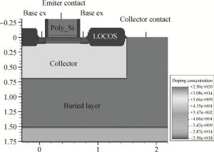
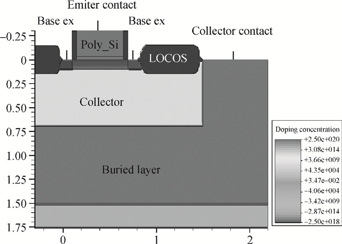
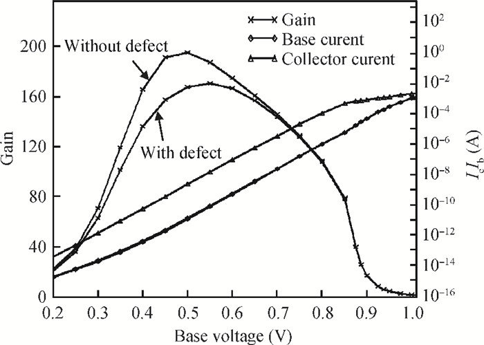
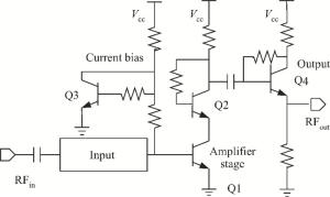
This paper addresses phase noise analysis of a radiofrequency LC oscillator built around a SiGe heterojunction bipolar transistor (HBT) realized in a 0.35 μm BiCMOS process, as an active device. First, we give a brief background to SiGe HBT device physics. The key point is to initiate quantitative analysis on the influence of defects induced during extrinsic base implantation on electric performances of this device. These defects are responsible for the current fluctuations at the origin of low frequency noise in BiCMOS technologies. Next, we investigate the effect of implantation defects as a source of noise in semiconductors on the phase noise of a radiofrequency LC oscillator. We observe their influence on the oscillator phase noise, and we quantify the influence of their energy distribution in the semiconductor gap. Second, we give a behavioral model of an LC oscillator containing a SiGe HBT as an active device. The key goal is to study the susceptibility of a radiofrequency oscillator built around a SiGe HBT to phase noise disturbance sources. Based on the time variance behavior of phase noise in oscillators, transient simulations (in the time domain) were used to analyze the time-dependent noise sensitivity of the oscillator.
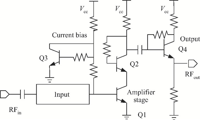
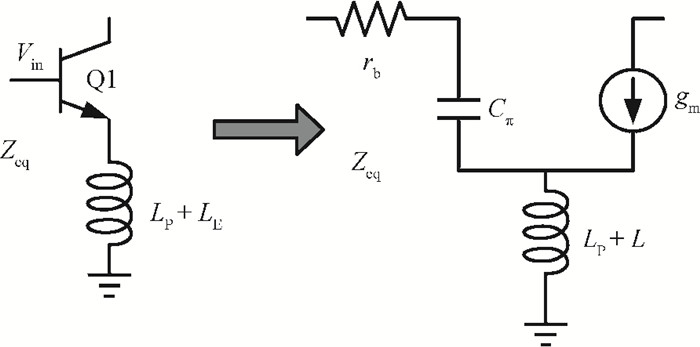
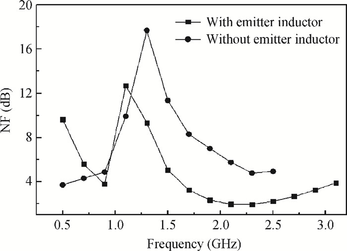
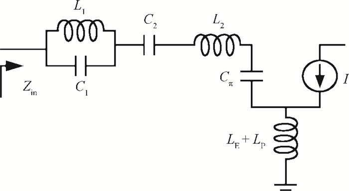
This paper presents design and implementation of a dual-band LNA using a 0.35 μm SiGe HBT process for 0.9 GHz GSM and 2.4 GHz WLAN applications. PCB layout parasitic effects have a vital effect on circuit performance and are accounted for using electro-magnetic (EM) simulation. Design considerations of noise decoupling, input/output impedance matching, and current reuse are described in detail. At 0.9/2.4 GHz, gain and noise figure are 13/16 dB and 4.2/3.9 dB, respectively. Both S11 and S22 are below-10 dB. Power dissipation is 40 mW at 3.5 V supply.


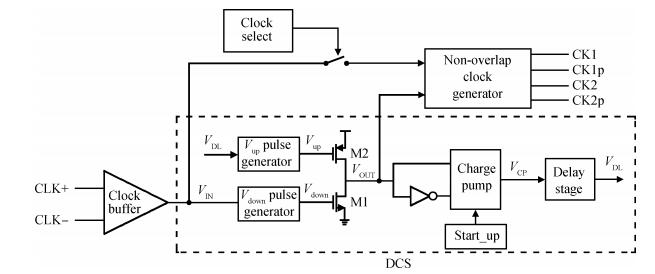
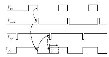
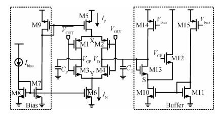
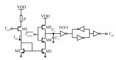
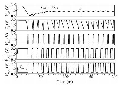
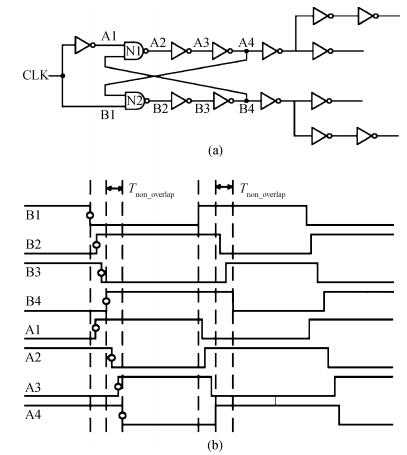
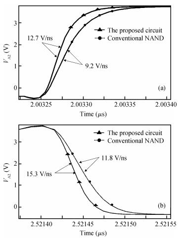
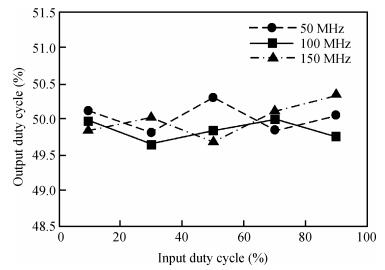
A clock generator circuit for a high-speed high-resolution pipelined A/D converter is presented. The circuit is realized by a delay locked loop (DLL), and a new differential structure is used to improve the precision of the charge pump. Meanwhile, a dynamic logic phase detector and a three transistor NAND logic circuit are proposed to reduce the output jitter by improving the steepness of the clock transition. The proposed circuit, designed by SMIC 0.18 μm 3.3 V CMOS technology, is used as a clock generator for a 14 bit 100 MS/s pipelined ADC. The simulation results have shown that the duty cycle ranged from 10% to 90% and can be adjusted. The average duty cycle error is less than 1%. The lock-time is only 13 clock cycles. The active area is 0.05 mm2 and power consumption is less than 15 mW.


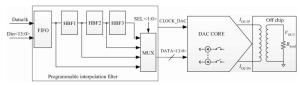
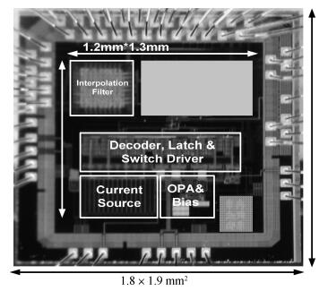
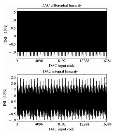
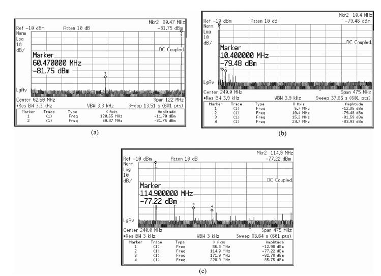
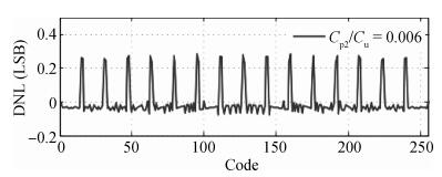
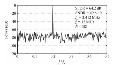
A programmable 14-bit 1-GS/s current-steering digital-to-analog converter is presented. It features a selectable interpolation rate (2x/4x/8x) with a programmable interpolation filter. To improve the high-frequency performance, a "fast switching" technique that adds additional biasing to the current-switch is adopted. The data-dependent clock loading effect is also minimized with an improved switch control by using a double latch. This DAC is implemented in 65 nm CMOS technology with an active area of 1.56 mm2. The measured SFDRs are 70.05 dB at 250 MS/s for 120.65 MHz input sine-wave signal and 64.24 dB at 960 MS/s for 56.3 MHz input sine-wave signal, respectively.


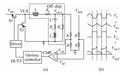
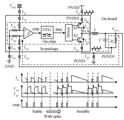
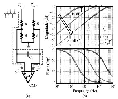
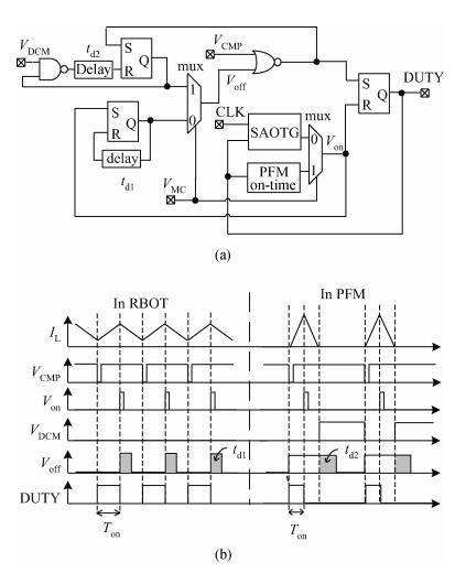
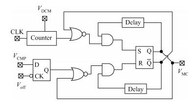
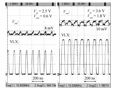
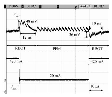
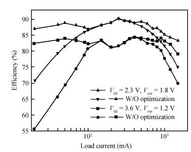
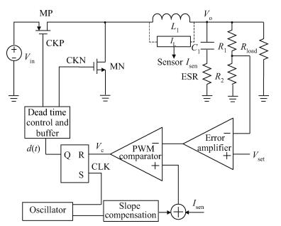
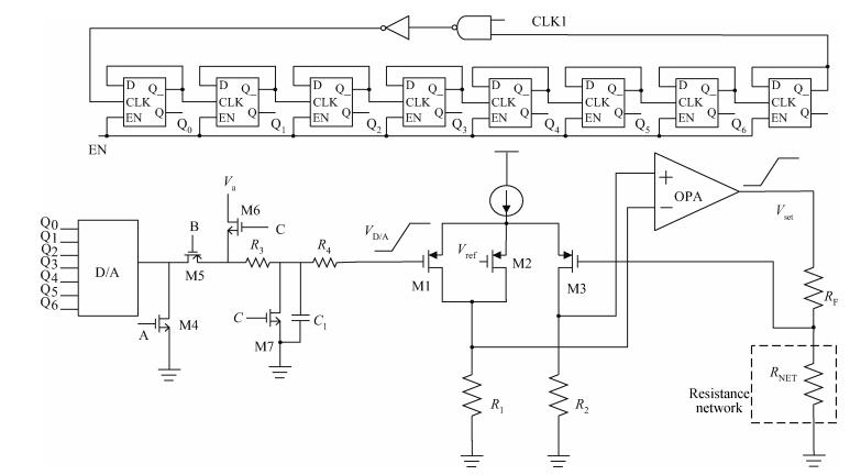
A 10 MHz ripple-based on-time controlled buck converter is presented. A novel low-cost dual ripple compensation, which consists of coupling capacitor compensation and passive equivalent series resistance compensation, is proposed to achieve a fast load transient response and robust stability simultaneously. Implemented in a 2P4M 0.35 μm CMOS process, the converter achieves fix-frequency output with a ripple of below 10 mV and an overshoot of 10 mV at 400 mA step load transient response. With width optimization of the power transistors in an ultra-heavy load and PFM control in a light load, the efficiency stays at over 83% for a load range from 20 mA to 1.5 A and the peak efficiency reaches 90.16%.


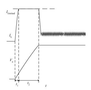
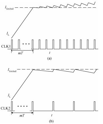
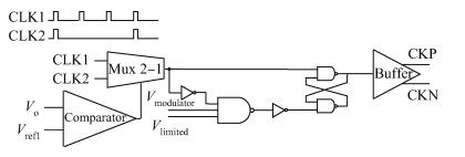
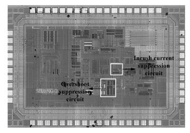
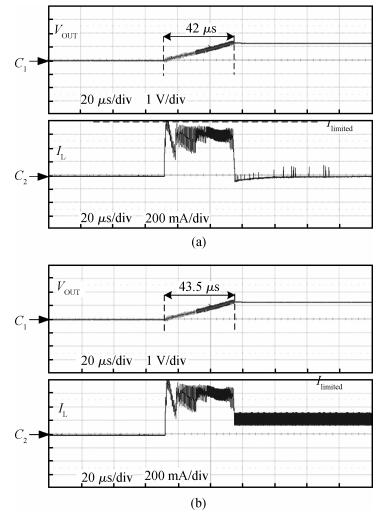
A fully integrated soft-start circuit for DC-DC buck converters is presented. The proposed high speed soft-start circuit is made of two sections:an overshoot suppression circuit and an inrush current suppression circuit. The overshoot suppression circuit is presented to control the input of the error amplifier to make output voltage limit increase in steps without using an external capacitor. A variable clock signal is adopted in the inrush current suppression circuit to increase the duty cycle of the system and suppress the inrush current. The DC-DC converter with the proposed soft-start circuit has been fabricated with a standard 0.13 μm CMOS process. Experimental results show that the proposed high speed soft-start circuit has achieved less than 50 μs start-up time. The inductor current and the output voltage increase smoothly over the whole load range.


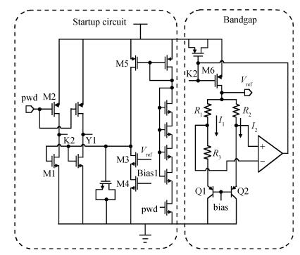
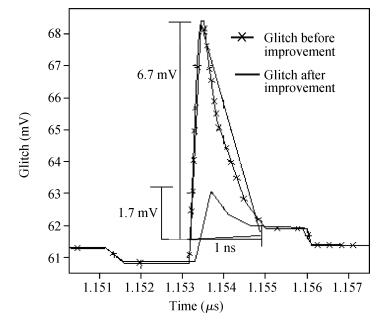
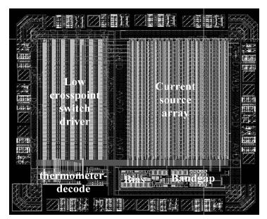
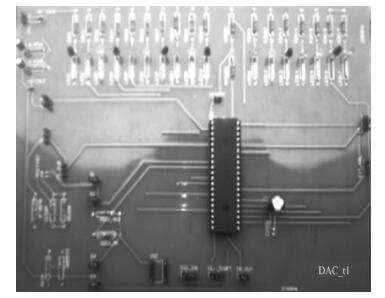
A 12-bit, 100-MHz CMOS current-steering D/A converter for CNC (computer number control) systems is presented. To reduce the glitch and increase the SFDR (spurious-free dynamic range), a low crosspoint switch driver and a special dummy switch are applied. In addition, a 4-5-3 segmental structure is used to optimize the performance and layout area. After improvement, the biggest glitch energy decreased from 6.7 pVs to 1.7 pVs, the INL decreased from 2 LSB to 0.8 LSB, the SFDR is 78 dB at a 100-MSPS clock rate and 1 MHz output frequency. This DAC can deliver up to 20.8 mA full-scale current into a 50 Ω load. The power when operating at full-scale current is 163 mW. The layout area is 1.8×1.8 mm2 in a standard 0.35-μm CMOS technology.


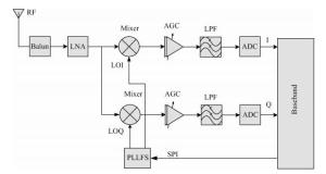
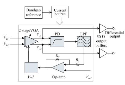
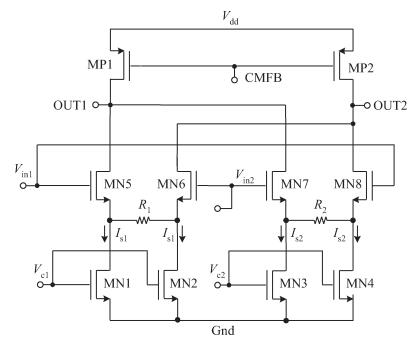
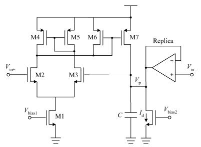
A differential automatic gain control (AGC) circuit is presented. The AGC architecture contains two-stage variable gain amplifiers (VGAs) which are implemented with a Gilbert cell, a peak detector (PD), a low pass filter, an operational amplifier, and two voltage to current (V-I) convertors. One stage VGA achieves 30 dB gain due to the use of active load. The AGC circuit is implemented in UMC 0.18-μm single-poly six-metal CMOS process technology. Measurement results show that the final differential output swing of the 2nd stage VGA is about 0.9-Vpp; the total gain of the two VGAs can be varied linearly from-10 to 50 dB when the control voltage varies from 0.3 to 0.9 V. The final circuit (containing output buffers and a band-gap reference) consumes 37 mA from single 1.8 V voltage supply. For a 50 mV amplitude 60% modulation depth input AM signal it needs 100 μs to stabilize the output. The frequency response of the circuit has almost a constant-3 dB bandwidth of 2.2 MHz. Its OIP3 result is at 19 dBm.


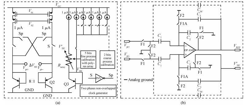
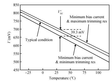
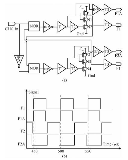
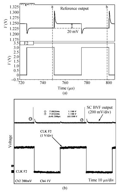
A switched capacitor bandgap voltage reference with correlated double sampling structure embedded in a temperature sensor is implemented in a standard 0.35 μm CMOS process. Due to the smaller change of the op-amp's output voltage, this topology is very suitable for low power applications. In addition, errors caused by the finite op-amp gain, input offset voltage, and 1/f noise are eliminated with the correlated double sampling technique. Additionally, two-level process calibration techniques are designed to minimize the process spread. Finally, a method of getting a full period valid reference voltage output is discussed and experimental results are provided to verify the effectiveness of the proposed structure.


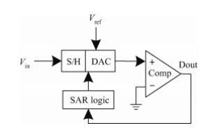
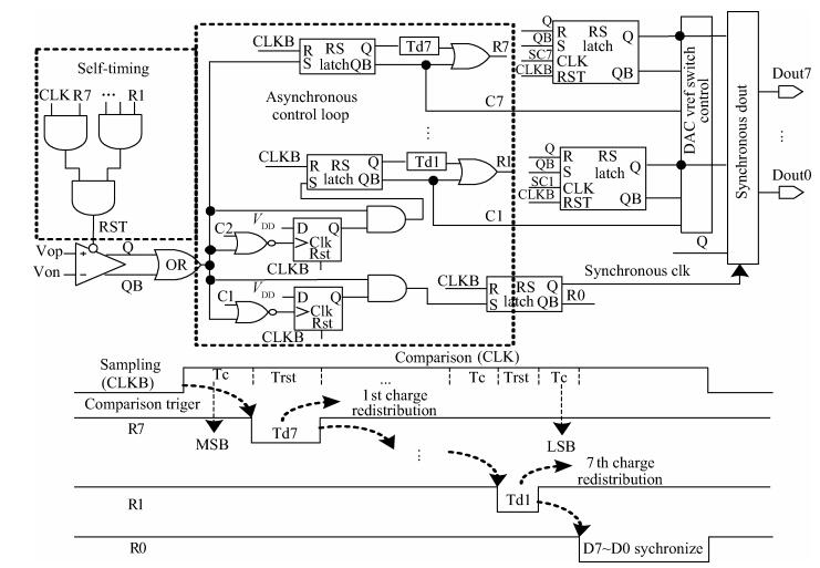
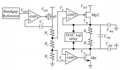
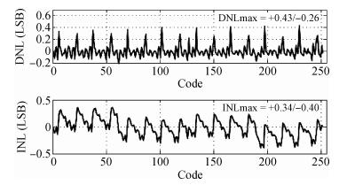
This paper proposes an 8 bit asynchronous successive approximation register ADC for wireless transceivers. A split capacitor DAC is used to reduce power and area consumption and the value of the split capacitor is calculated theoretically to ensure linearity. Asynchronous control logic is proposed to eliminate the high internal clocks and significantly speeds up the successive approximation algorithm. An on-chip reference with a fully integrated buffer and decoupling capacitor is adopted for avoiding an extra pin for the off-chip reference. The prototype, fabricated in UMC 0.18 μm CMOS technology, achieves an effective number of bits of 7.64 bits at a sampling frequency of 12 MS/s. The total power consumption is 0.918 mW for a 1.8 V supply, while the on-chip reference consumes 53% of the total power. It achieves a figure of merit of 180 fJ/conv·step, excluding the reference's power consumption.


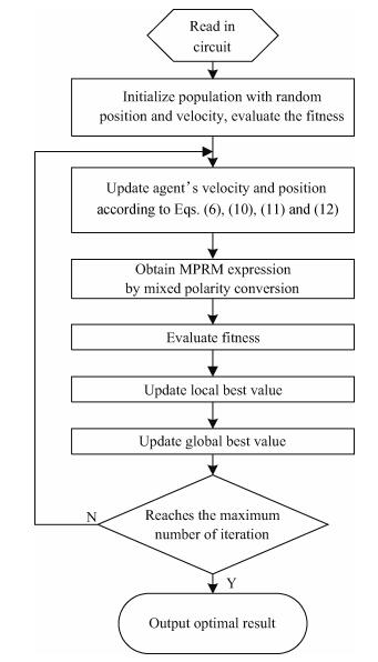
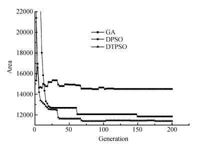
Having the advantage of simplicity, robustness and low computational costs, the particle swarm optimization (PSO) algorithm is a powerful evolutionary computation tool for synthesis and optimization of Reed-Muller logic based circuits. Exploring discrete PSO and probabilistic transition rules, the discrete ternary particle swarm optimization (DTPSO) is proposed for mixed polarity Reed-Muller (MPRM) circuits. According to the characteristics of mixed polarity OR/XNOR expression, a tabular technique is improved, and it is applied in the polarity conversion of MPRM functions. DTPSO is introduced to search the best polarity for an area of MPRM circuits by building parameter mapping relationships between particles and polarities. The computational results show that the proposed DTPSO outperforms the reported method using maxterm conversion starting from POS Boolean functions. The average saving in the number of terms is about 11.5%; the algorithm is quite efficient in terms of CPU time and achieves 12.2% improvement on average.


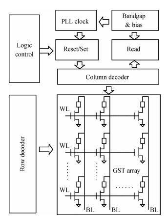
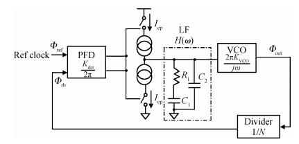
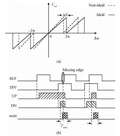
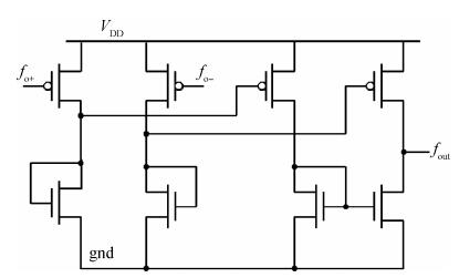
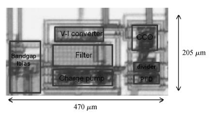
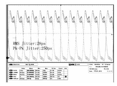
A fully integrated low-jitter, precise frequency CMOS phase-locked loop (PLL) clock for the phase change memory (PCM) drive circuit is presented. The design consists of a dynamic dual-reset phase frequency detector (PFD) with high frequency acquisition, a novel low jitter charge pump, a CMOS ring oscillator based voltage-controlled oscillator (VCO), a 2nd order passive loop filter, and a digital frequency divider. The design is fabricated in 0.35 μm CMOS technology and consumes 20 mW from a supply voltage of 5 V. In terms of the PCM's program operation requirement, the output frequency range is from 1 to 140 MHz. For the 140 MHz output frequency, the circuit features a cycle-to-cycle jitter of 28 ps RMS and 250 ps peak-to-peak.


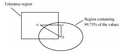
After analyzing the multivariate Cpm method (Chan et al. 1991), this paper presents a spatial multivariate process capability index (PCI) method, which can solve a multivariate off-centered case and may provide references for assuring and improving process quality level while achieving an overall evaluation of process quality. Examples for calculating multivariate PCI are given and the experimental results show that the systematic method presented is effective and actual.