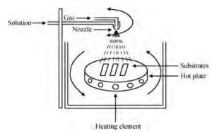
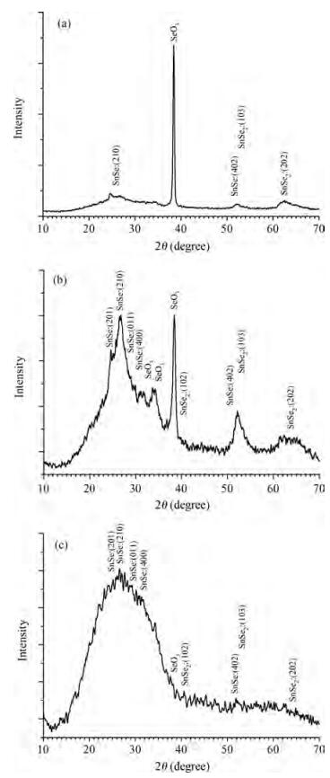
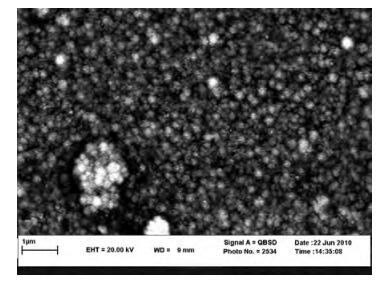
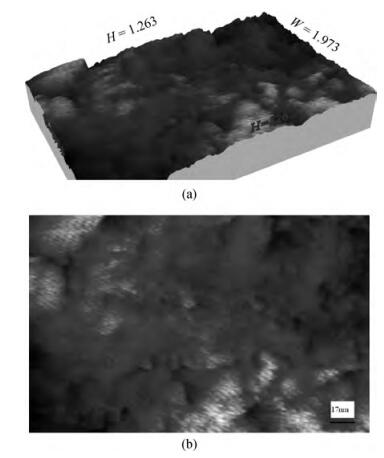
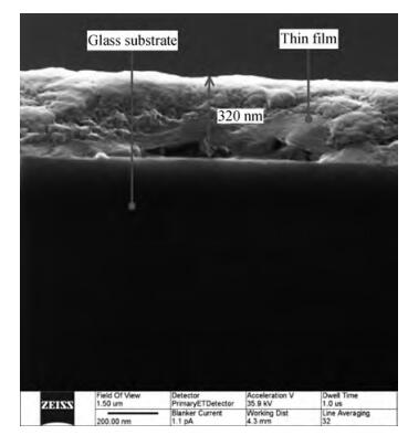
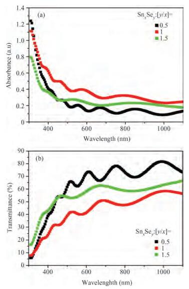
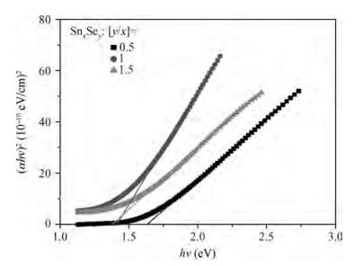
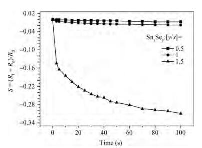
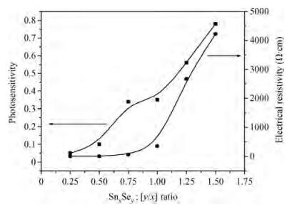
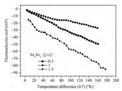
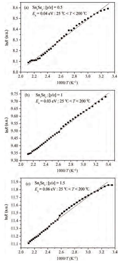
Thin films of tin selenide (SnxSey) with an atomic ratio of $r=\left[\frac{y}{x}\right]=0.5$, 1 and 1.5 were prepared on a glass substrate at T=470℃ using a spray pyrolysis technique. The initial materials for the preparation of the thin films were an alcoholic solution consisting of tin chloride (SnCl4· 5H2O) and selenide acide (H2SeO3). The prepared thin films were characterized by X-ray diffraction (XRD), scanning electron microscopy, scanning tunneling microscopy, scanning helium ion microscopy, and UV-vis spectroscopy. The photoconductivity and thermoelectric effects of the SnxSey thin films were then studied. The SnxSey thin films had a polycrystalline structure with an almost uniform surface and cluster type growth. The increasing atomic ratio of r in the films, the optical gap, photosensitivity and Seebeck coefficient were changed from 1.6 to 1.37 eV, 0.01 to 0.31 and -26.2 to -42.7 mV/K (at T=350 K), respectively. In addition, the XRD patterns indicated intensity peaks in r=1 that corresponded to the increase in the SnSe and SnSe2 phases.

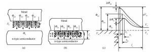
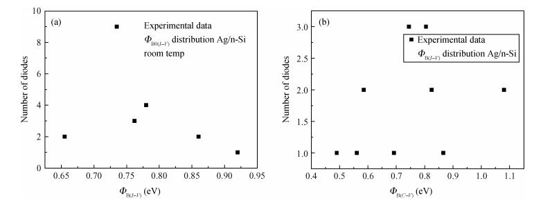
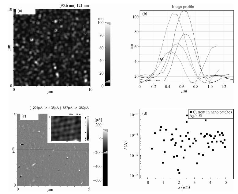
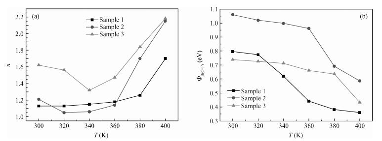
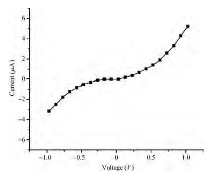
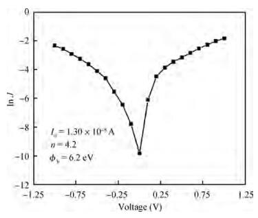
Schottky diodes with an Ag/n-Si/W/Cu structure and 100 μm in diameter were studied. Analyzing the silver metal surface coating on the n-Si substrate using a scanning probe microscopy (SPM) device showed a large number of nano patches in the surface with dimensions of 0 to 100 nm. The potential distribution of the patches revealed that the potential of each patch with the neighboring patches was different. The electrical characteristics of the devices were studied between temperature ranges of 300 and 380 K. When the temperature ideality factor approximately increases, the potential barrier height decreases. The potential barrier height was calculated separately from the I-V and C-V characteristics. The main reasons for the significant difference between room temperature and higher temperatures were the differences in patch distribution, the different potentials of each patch, and the interactions between them. The effective potential barrier height depended on the degree of inhomogeneity, and thus the operating potential barrier height in the contact surface was smaller than the average value, and the ideality factor was more than unitary. With the increase in the potential value, the ideality factor becomes close to unitary, and with increasing temperatures, the ideality factor is increased. In this case, the maximum potential barrier height accrues at a greater distance from the metal contact. For this reason, at high temperatures the average value of the potential barrier height is smaller. Moreover, with increasing temperature, the ideality factor is increased.


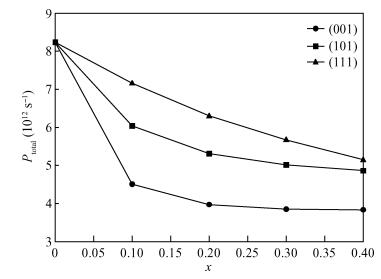
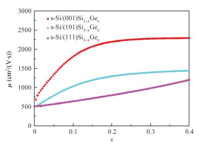
We aim to establish a model of the averaged hole mobility of strained Si grown on (001), (101), and (111) relaxed Si1-xGex substrates. The results obtained from our calculation show that their hole mobility values corresponding to strained Si (001), (101) and (111) increase by at most about three, two and one times, respectively, in comparison with the unstrained Si. The results can provide a valuable reference to the understanding and design of strained Si-based device physics.
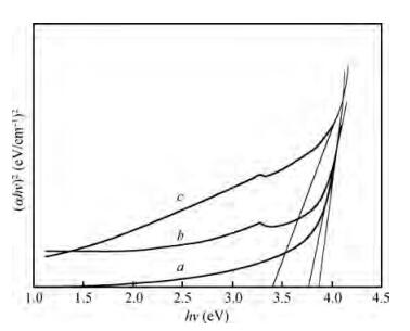
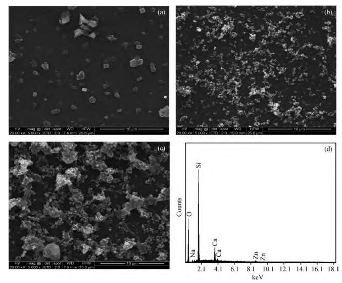
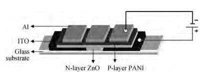
Polyaniline, ZnO and polyaniline/ZnO nanocomposite thin films are coated on glass substrates using the spray pyrolysis technique. The samples are characterized by the XRD, SEM, EDAX, UV-Vis and I-V characteristics. The XRD analyses confirm that the spray-coated polyaniline and ZnO thin films have orthorhombic and hexagonal structures, respectively, and optical bandgap energy decreases from 3.81 to 3.41 eV with the addition of a Zn atom. SEM analysis of the polyaniline/ZnO nanocomposite thin films shows that there is an agglomeration of ZnO particles with uniform distribution in the polyaniline matrix, and the diode characteristics of the polyaniline/ZnO nanocomposite show weak rectification behavior. Parameters such as the ideality factor, reverse saturation current and barrier height are calculated from the I-V characteristics.

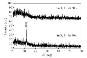
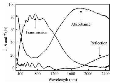
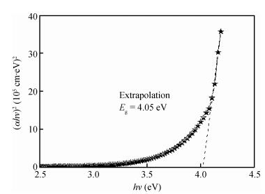
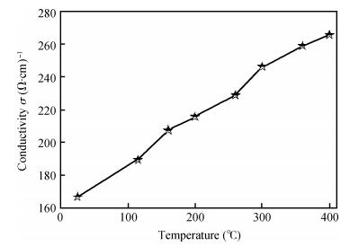
We studied fluorine-doped tin oxide on a glass substrate at 350℃ using an ultrasonic spray technique. Tin (Ⅱ) chloride dehydrate, ammonium fluoride dehydrate, ethanol and NaOH were used as the starting material, dopant source, solvent and stabilizer, respectively. The SnO2:F thin films were deposited at 350℃ and a pending time of 60 and 90 s. The as-grown films exhibit a hexagonal wurtzite structure and have (101) orientation. The G=31.82 nm value of the grain size is attained from SnO2:F film grown at 90 s, and the transmittance is greater than 80% in the visible region. The optical gap energy is found to measure 4.05 eV for the film prepared at 90 s, and the increase in the electrical conductivity of the film with the temperature of the sample is up to a maximum value of 265.58 (Ω ·cm) -1, with the maximum activation energy value of the films being found to measure 22.85 meV, indicating that the films exhibit an n-type semiconducting nature.


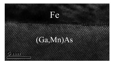
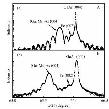
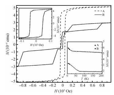
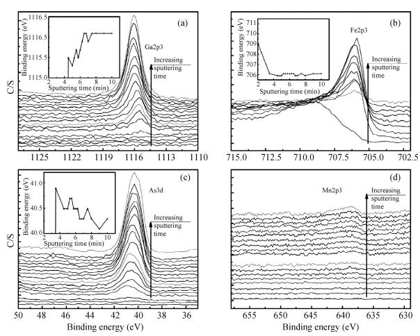
Fe/(Ga, Mn)As heterostructures were fabricated by all molecular-beam epitaxy. Double-crystal X-ray diffraction and high-resolution cross-sectional transmission electron micrographs show that the Fe layer has a well ordered crystal orientation and an abrupt interface. The different magnetic behavior between the Fe layer and (Ga, Mn)As layer is observed by superconducting quantum interference device magnetometry. X-ray photoelectron spectroscopy measurements indicate no Fe2As and Fe-Ga-As compounds, i.e., no dead magnetic layer at the interface, which strongly affects the magnetic proximity and the polarization of the Mn ion in a thin (Ga, Mn)As region near the interface of the Fe/(Ga, Mn)As heterostructure.
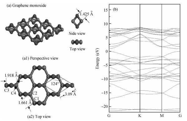
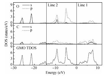
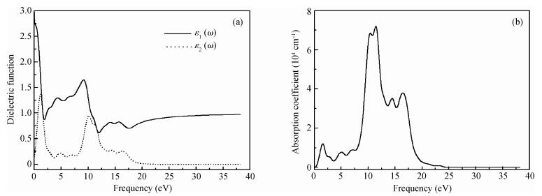
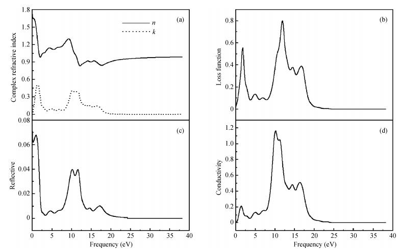
The electronic and optical properties of graphene monoxide, a new type of semiconductor material, are theoretically studied by first-principles density functional theory. The calculated band structure shows that graphene monoxide is a semiconductor with a direct band gap of 0.95 eV. The density of states of graphene monoxide and the partial density of states for C and O are given to understand the electronic structure. In addition, we calculate the optical properties of graphene monoxide, including the complex dielectric function, absorption coefficient, complex refractive index, loss-function, reflectivity and conductivity. These results provide a physical basis for potential application in optoelectronic devices.


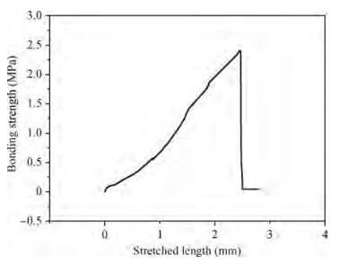
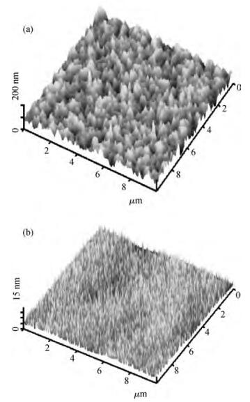
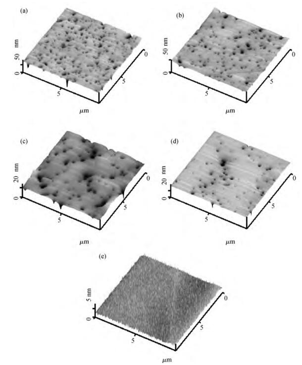
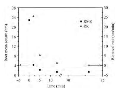
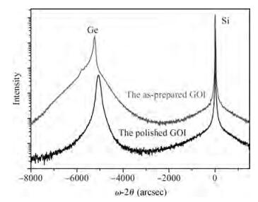
We prepared germanium-on-insulator (GOI) substrates by using Smart-CutTM and wafer bonding technology. The fabricated GOI is appropriate for polishing due to a strong bonding strength (2.4 MPa) and a sufficient bonding quality. We investigated mechanical polishing and chemical-mechanical polishing (CMP) systematically, and an appropriate polishing method——mechanical polishing combined with CMP——is obtained. As shown by AFM measurement, the RMS of GOI after polishing decreased to 0.543 nm. And the Ge peak profile of the XRD curve became symmetric, and the FWHM is about 121.7 arcsec, demonstrating a good crystal quality.
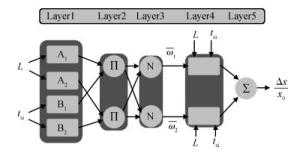
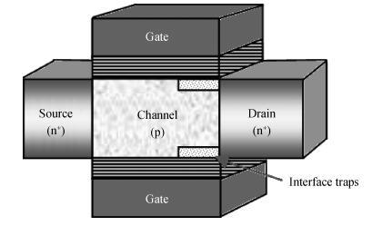
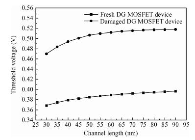
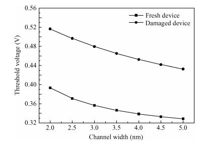
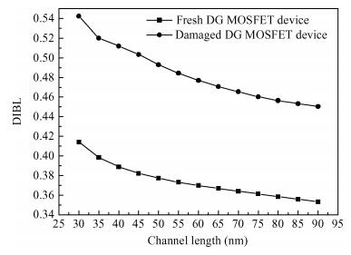
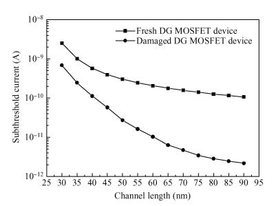
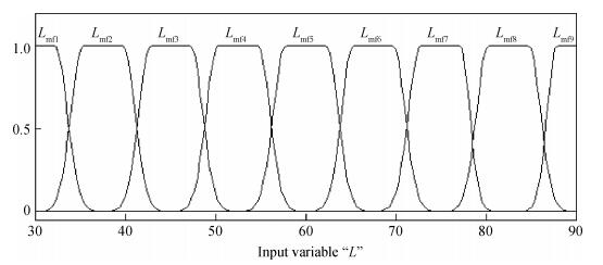
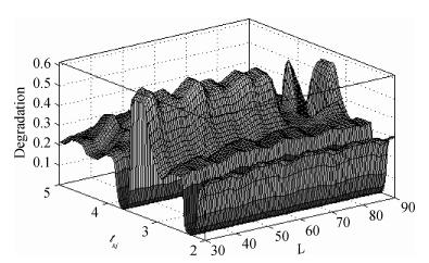
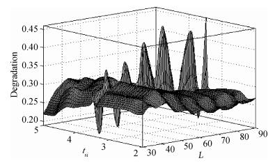
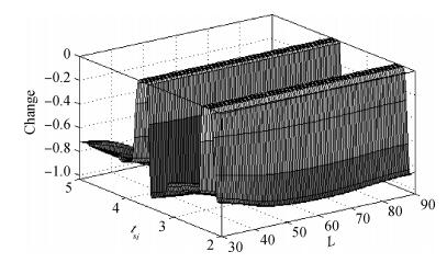
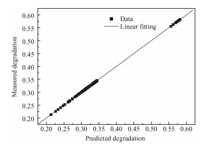
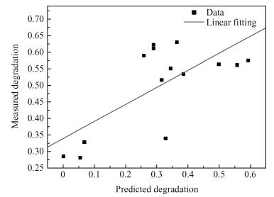
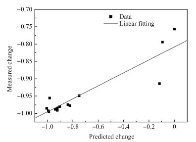
A fuzzy framework based on an adaptive network fuzzy inference system (ANFIS) is proposed to evaluate the relative degradation of the basic subthreshold parameters due to hot-carrier effects for nanoscale thin-film double-gate (DG) MOSFETs. The effect of the channel length and thickness on the resulting degradation is addressed, and 2-D numerical simulations are used for the elaboration of the training database. Several membership function shapes are developed, and the best one in terms of accuracy is selected. The predicted results agree well with the 2-D numerical simulations and can be efficiently used to investigate the impact of the interface fixed charges and quantum confinement on nanoscale DG MOSFET subthreshold behavior. Therefore, the proposed ANFIS-based approach offers a simple and accurate technique to study nanoscale devices, including the hot-carrier and quantum effects.


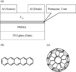
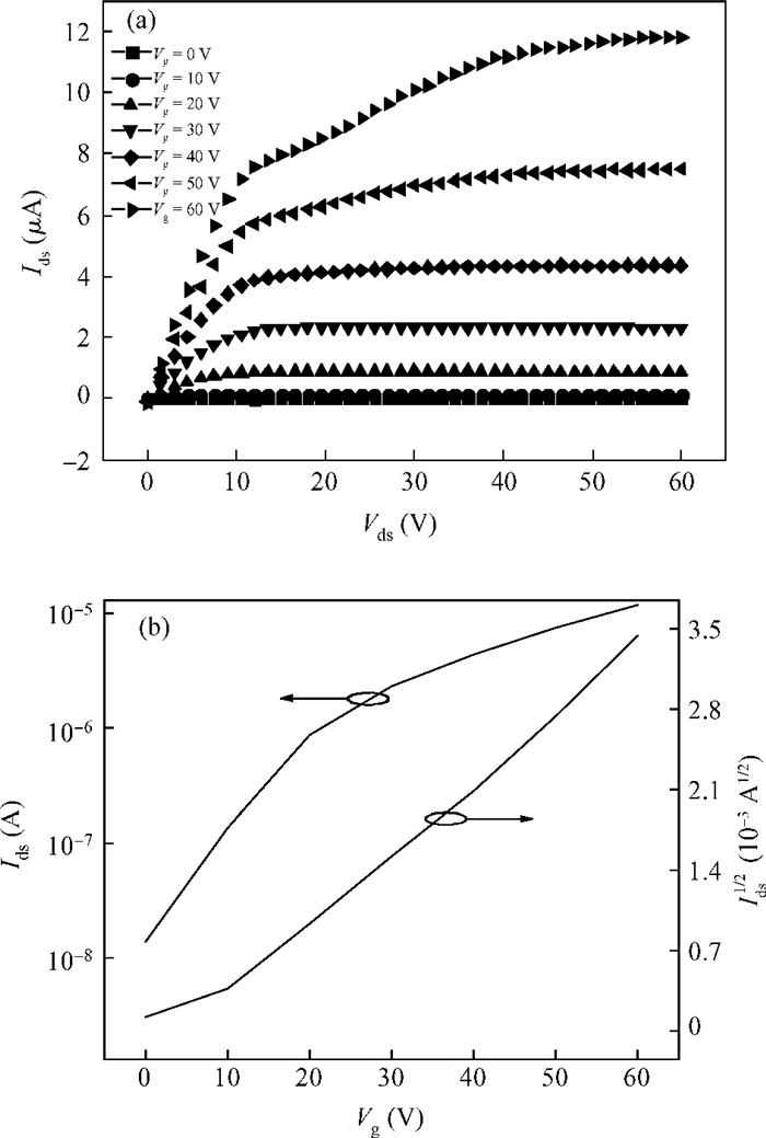
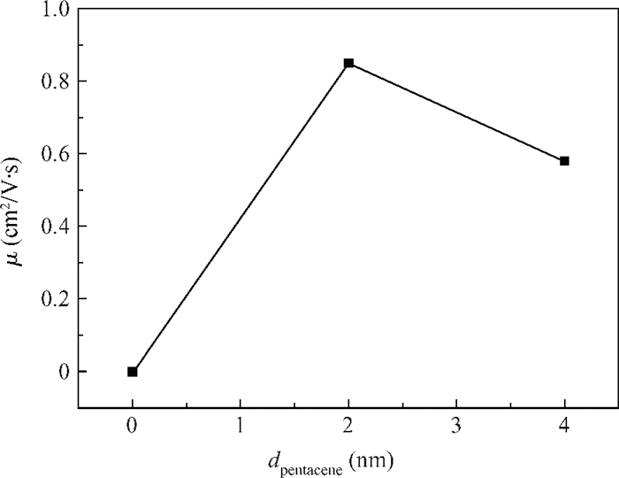
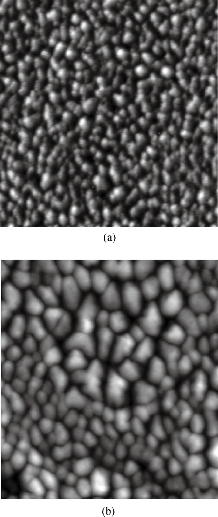
We investigated the properties of C60-based organic field-effect transistors (OFETs) with a pentacene passivation layer inserted between the C60 active layer and the gate dielectric. After modification of the pentacene passivation layer, the performance of the devices was considerably improved compared to C60-based OFETs with only a PMMA dielectric. The peak field-effect mobility was up to 1.01 cm2/(V·s) and the on/off ratio shifted to 104. This result indicates that using a pentacene passivation layer is an effective way to improve the performance of N-type OFETs.


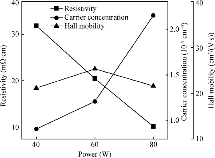
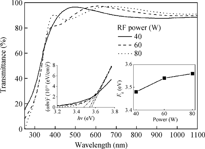
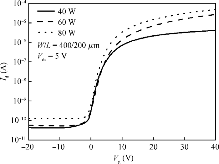
The influence of radio frequency (RF) power on the properties of magnetron sputtered amorphous indium gallium zinc oxide (a-IGZO) thin films and the related thin-film transistor (TFT) devices is investigated comprehensively. A series of a-IGZO thin films prepared with magnetron sputtering at various RF powers are examined. The results prove that the deposition rate sensitively depends on RF power. In addition, the carrier concentration increases from 0.91×10¹⁹ to 2.15×1019 cm-3 with the RF power rising from 40 to 80 W, which may account for the corresponding decrease in the resistivity of the a-IGZO thin films. No evident impacts of RF power are observed on the surface roughness, crystalline nature and stoichiometry of the a-IGZO samples. On the other hand, optical transmittance is apparently influenced by RF power where the extracted optical band-gap value increases from 3.48 to 3.56 eV with RF power varying from 40 to 80 W, as is supposed to result from the carrier-induced band-filling effect. The rise in RF power can also affect the performance of a-IGZO TFTs, in particular by increasing the field-effect mobility clearly, which is assumed to be due to the alteration of the extended states in a-IGZO thin films.

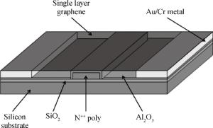
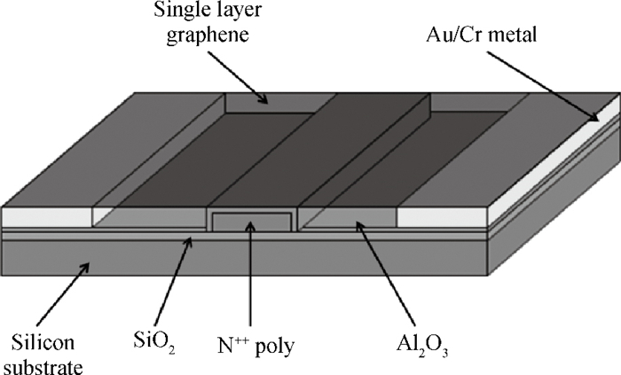
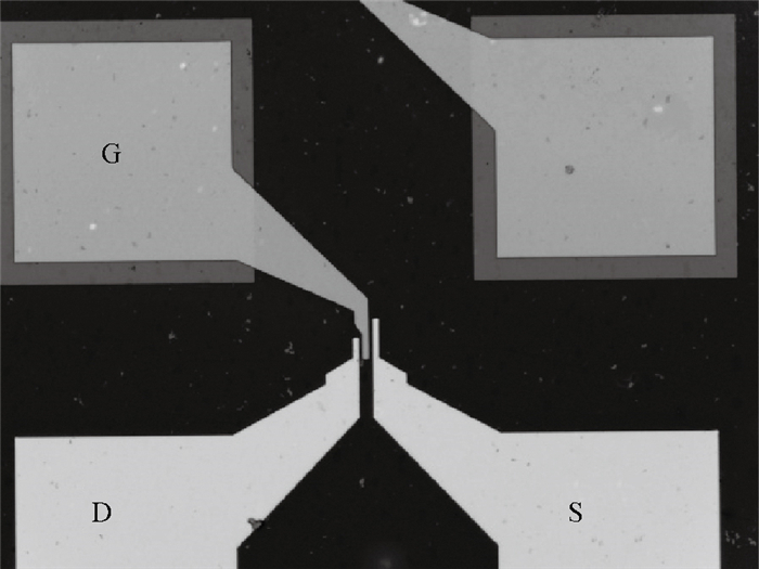
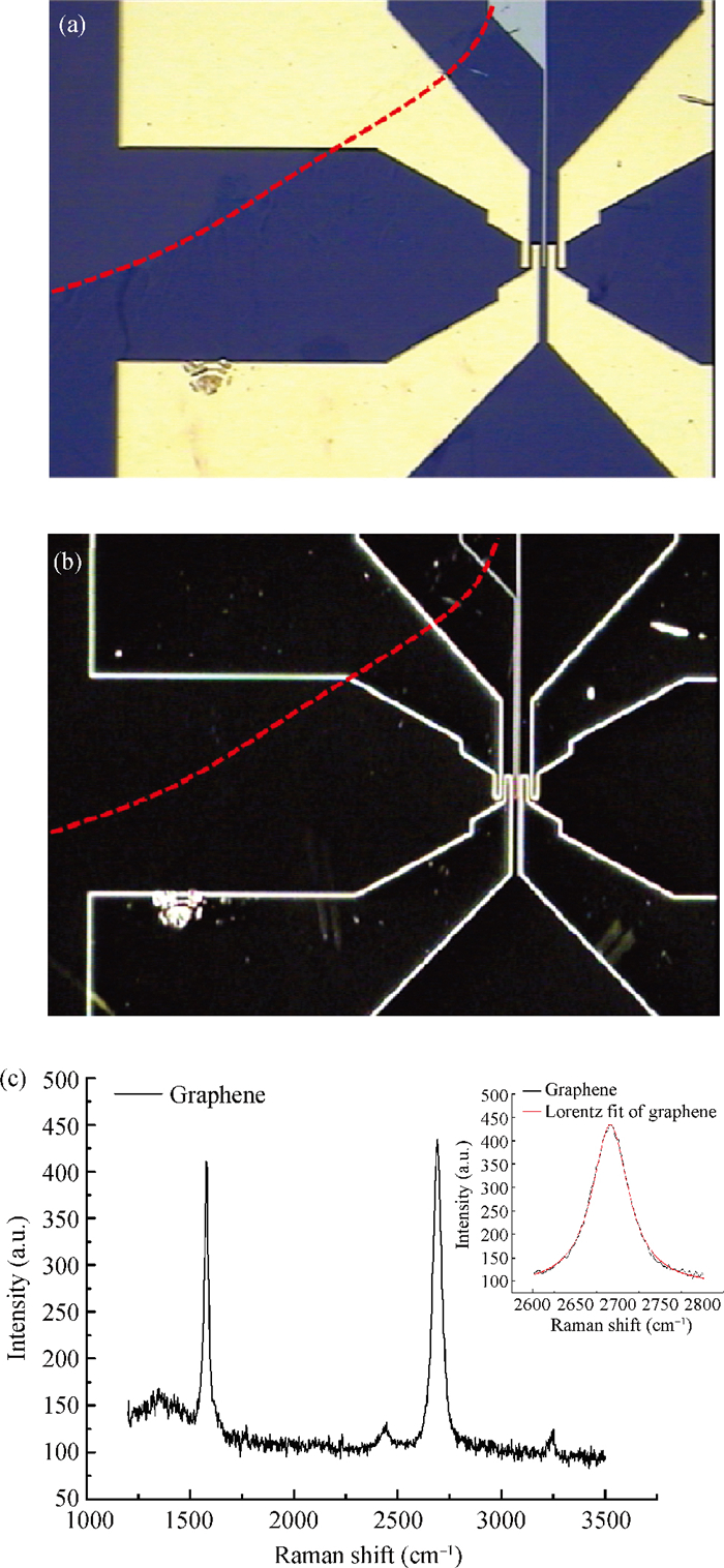
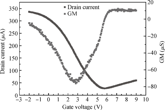
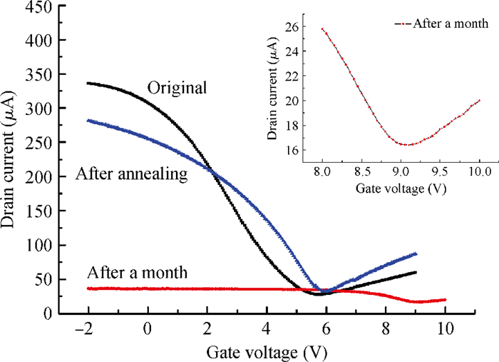
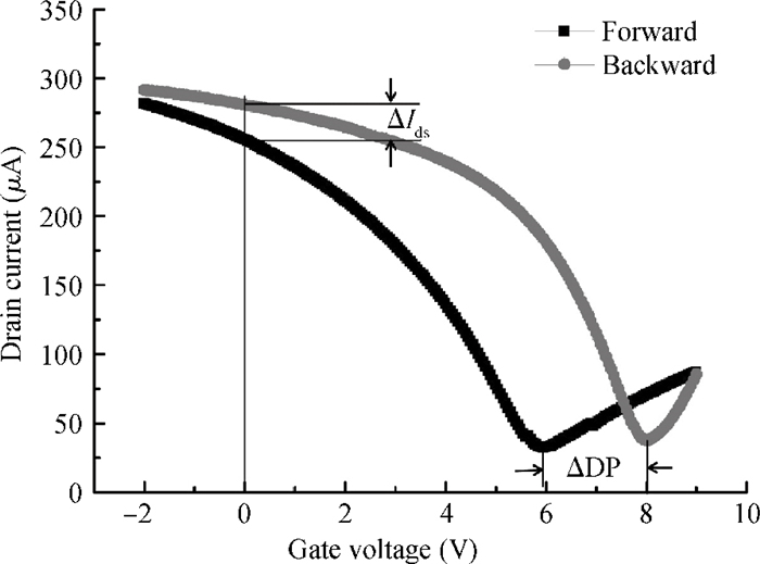
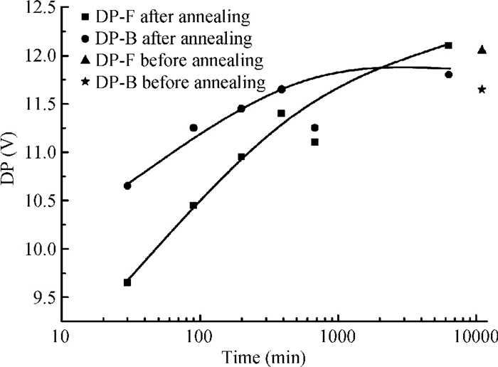
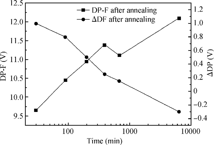
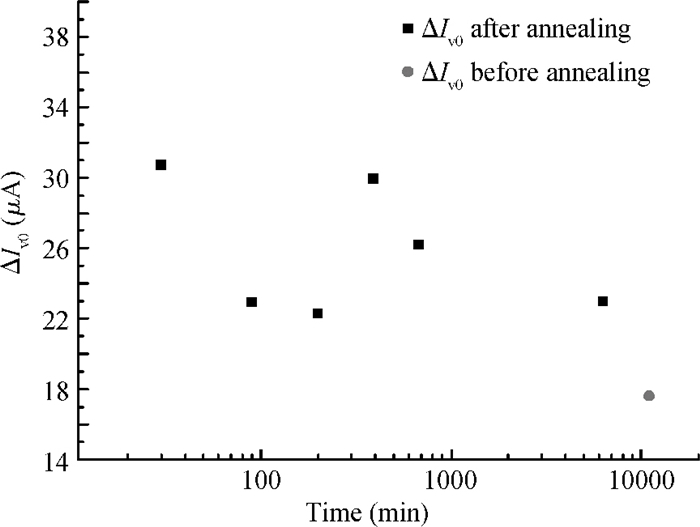
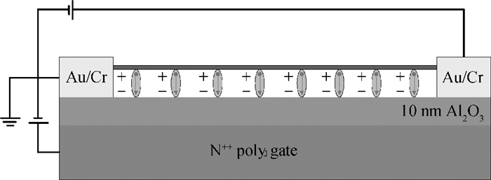
The stability of a graphene field effect transistor (GFET) is important to its performance optimization, and study of hysteresis behavior can propose useful suggestions for GFET fabrication and optimization. In this work, a back-gate GFET has been fabricated and characterized, which is compatible with the CMOS process. The stability of a GFET in air has been studied and it is found that a GFET's electrical performance dramatically changes when exposed to air. The hysteresis characteristic of a GFET depending on time has been observed and analyzed systematically. Hysteresis behavior is reversed at room temperature with the Dirac point positive shifted when the GFET is exposed to air after annealing.
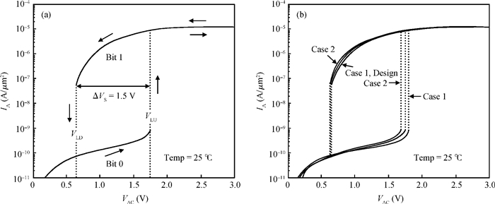
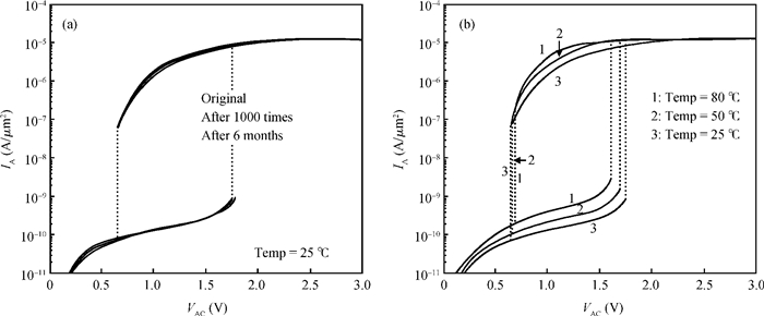
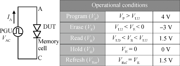
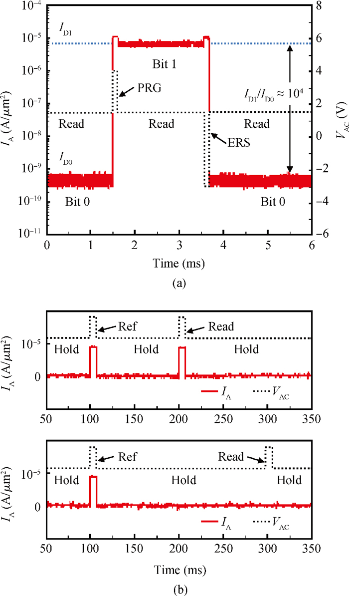
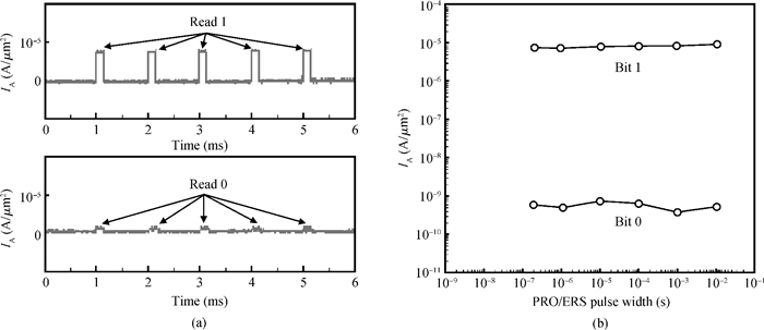
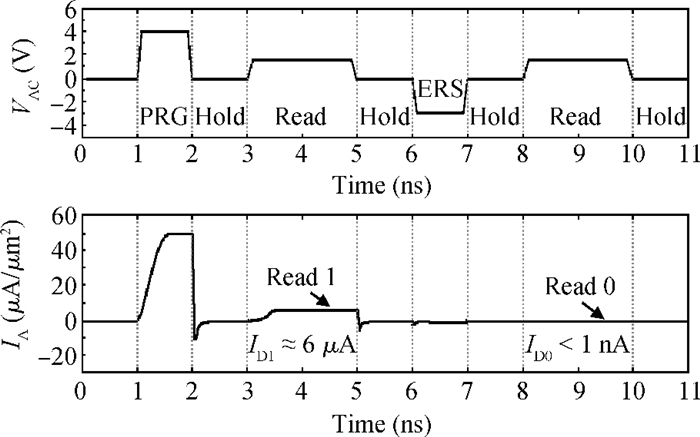
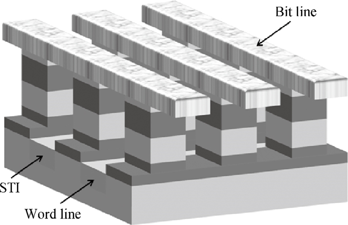
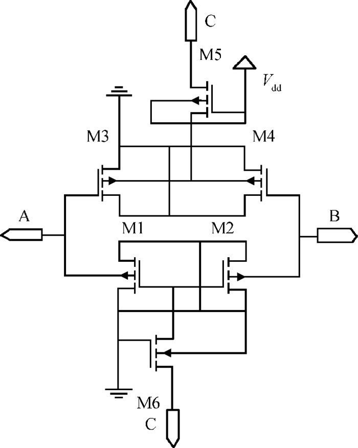
A two-port capacitorless PNPN device with high density, high speed and low power memory fabricated using standard CMOS technology is presented. Experiments and calibrated simulations were conducted which prove that this new memory cell has a high operation speed (ns level), large read current margin (read current ratio of 104×), low process variation, good thermal reliability and available retention time (190 ms). Furthermore, the new memory cell is free of the cyclic endurance/reliability problems induced by hot-carrier injection due to the gateless structure.

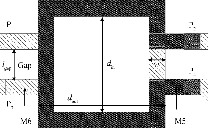
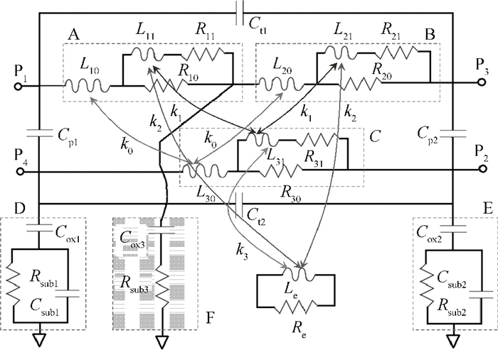
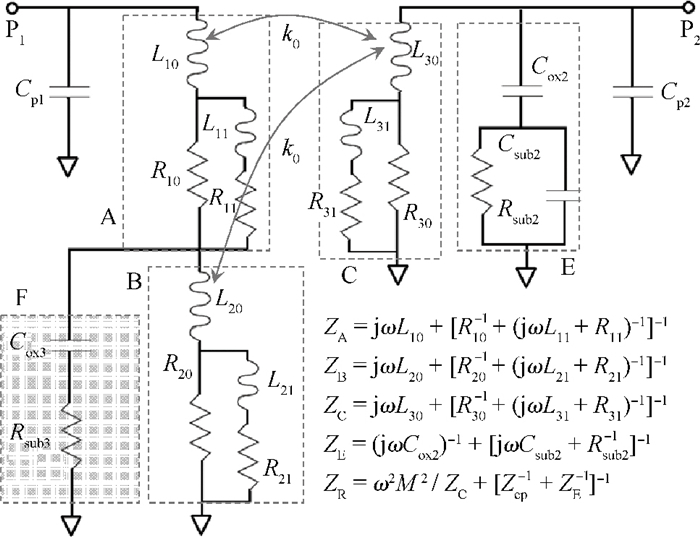
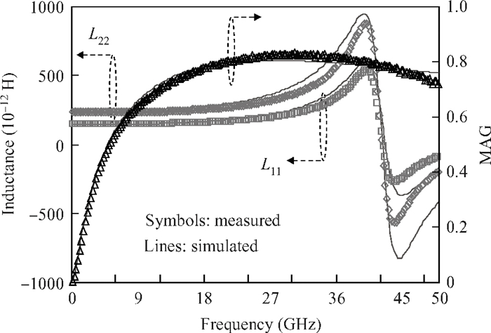
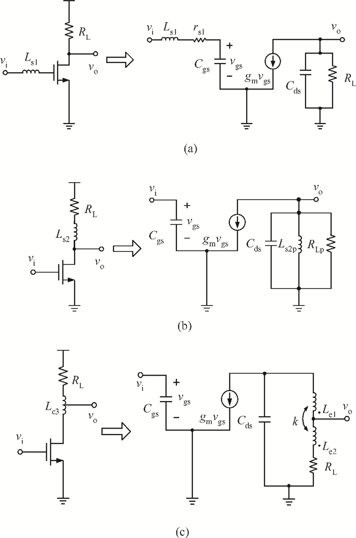
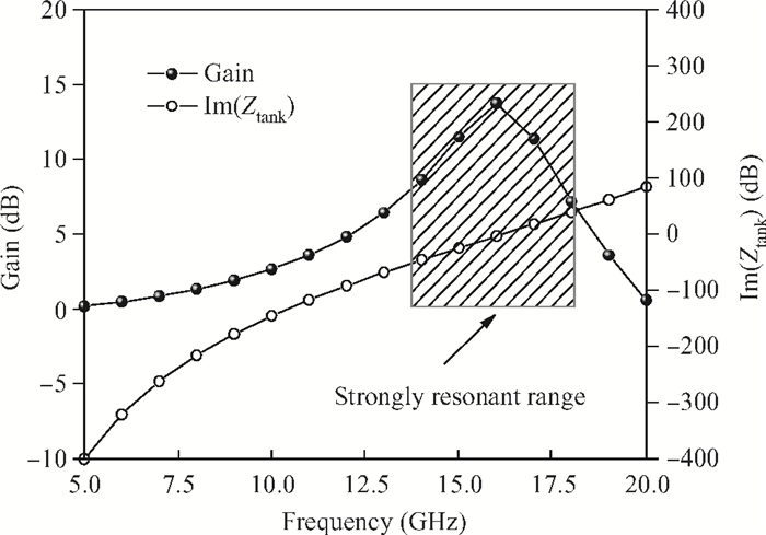
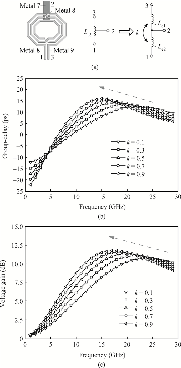
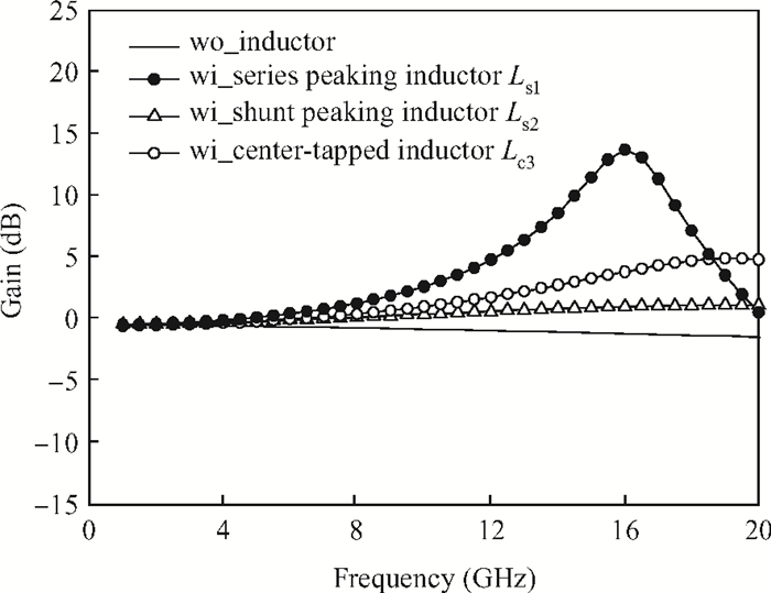
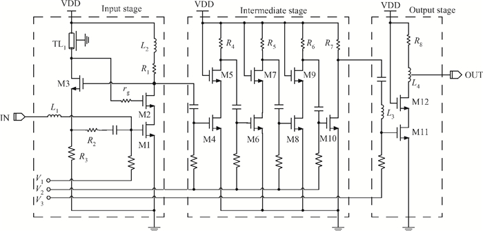
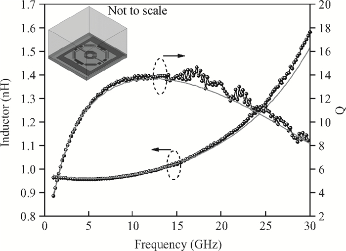
A novel compact model for on-chip stacked transformers is presented. The proposed model topology gives a clear distinction to the eddy current, resistive and capacitive losses of the primary and secondary coils in the substrate. A method to analytically determine the non-ideal parasitics between the primary coil and substrate is provided. The model is further verified by the excellent match between the measured and simulated S-parameters on the extracted parameters for a 1:1 stacked transformer manufactured in a commercial RF-CMOS technology.


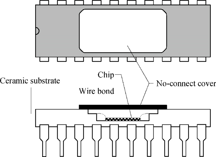
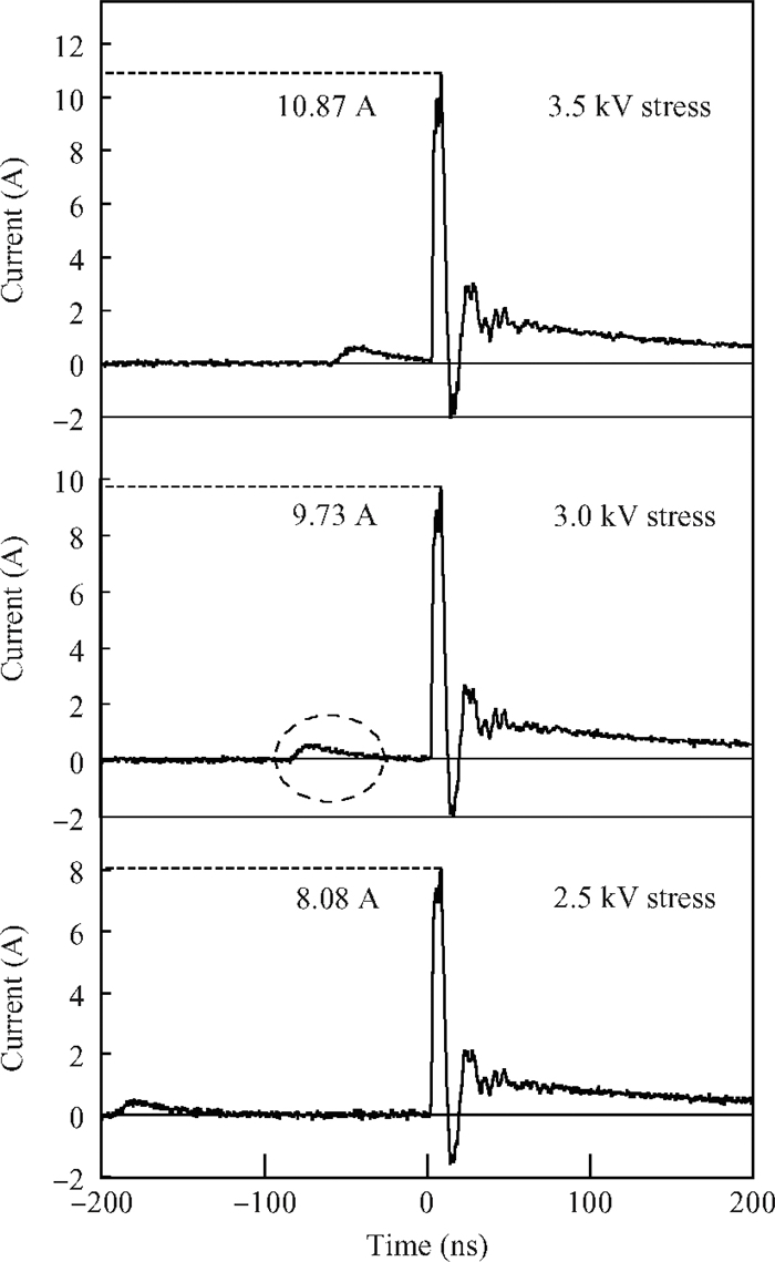
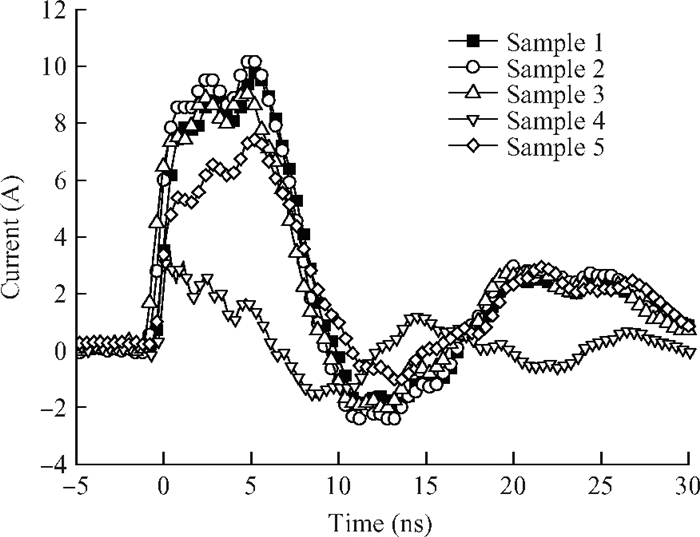
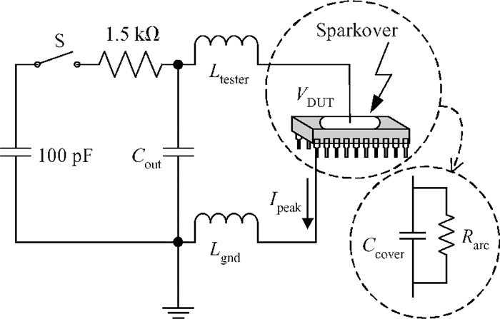
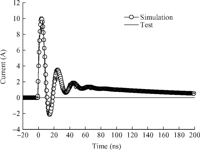
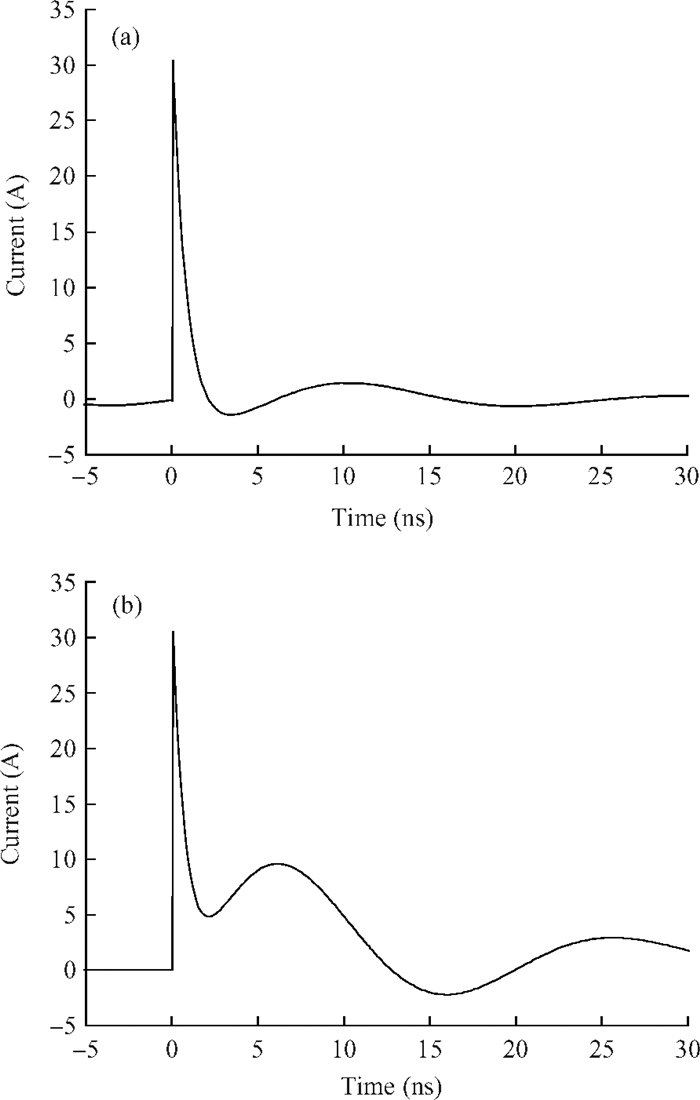
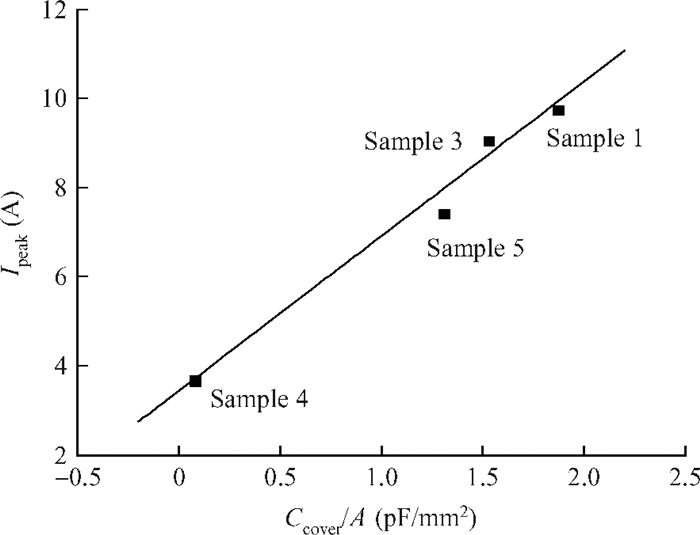
The human body model (HBM) stress of a no-connect metal cover is tested to obtain the characteristics of abnormal electrostatic discharge, including current waveforms and peak current under varied stress voltage and device failure voltage. A new discharge model called the "sparkover-induced model" is proposed based on the results. Then, failure mechanism analysis and model simulation are performed to prove that the transient peak current caused by a sparkover of low arc impedance will result in the devices' premature damage when the potential difference between the no-connect metal cover and the chip exceeds the threshold voltage of sparkover.
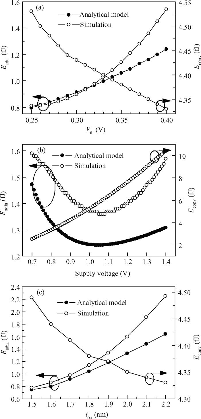
This paper presents an analytical model to study the scaling trends in energy recovery logic. The energy performance of conventional CMOS and energy recovery logic are compared with scaling the design and technology parameters such as supply voltage, device threshold voltage and gate oxide thickness. The proposed analytical model is validated with simulation results at 90 nm and 65 nm CMOS technology nodes and predicts the scaling behavior accurately that help us to design an energy-efficient CMOS digital circuit design at the nanoscale. This research work shows the adiabatic switching as an ultra-low-power circuit technique for sub-100 nm digital CMOS circuit applications.

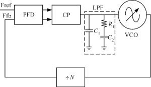
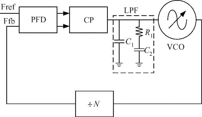
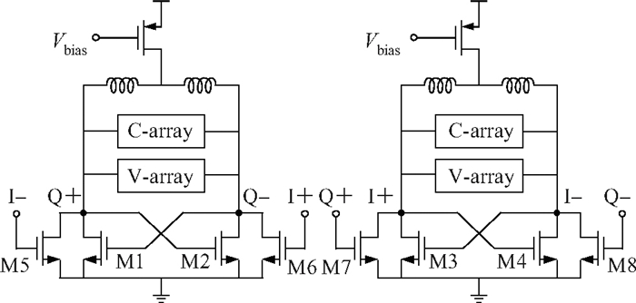
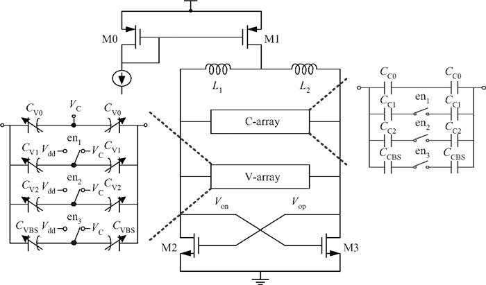
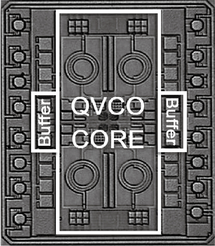
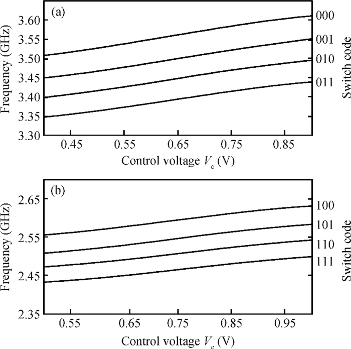
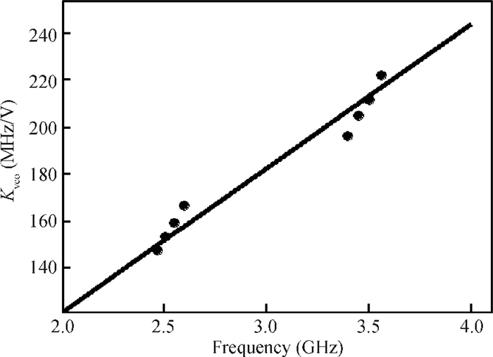
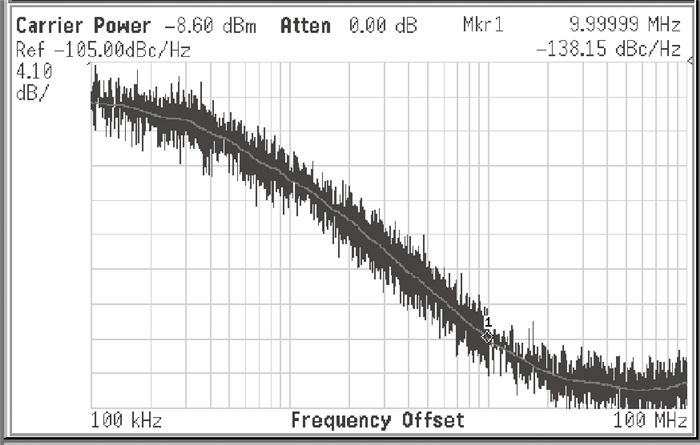
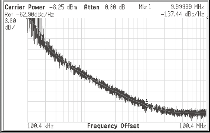
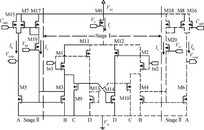
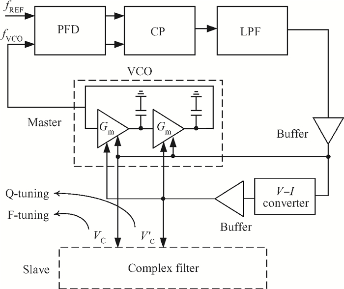
This paper presents a novel dual-band quadrature voltage controlled oscillator (VCO) with the gain proportional to the oscillation frequency. Frequency synthesizers with this VCO can reduce the bandwidth fluctuation over all the frequency ranges without compensation or calibration. Besides the original switched capacitor array, an extra switched varactor array is adopted for the implementation of the proposed VCO. The tuning technique of changing the values of the capacitor and varactor at the same ratio is also derived. For verification purposes, a 2.5 G/3.5 G dual-band quadrature VCO is fabricated in a 0.13 μm CMOS process for WiMAX applications. Measurement results show that the VCO gain is closely proportional to the oscillation frequency with ±16% variation over the entire frequency range. The phase noise is -138.15 dBc/Hz at 10 MHz from the 2.5 GHz carrier and -137.44 dBc/Hz at 10 MHz from the 3.5 GHz carrier.

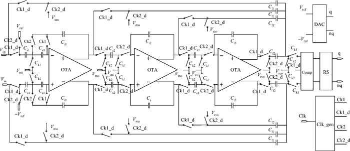
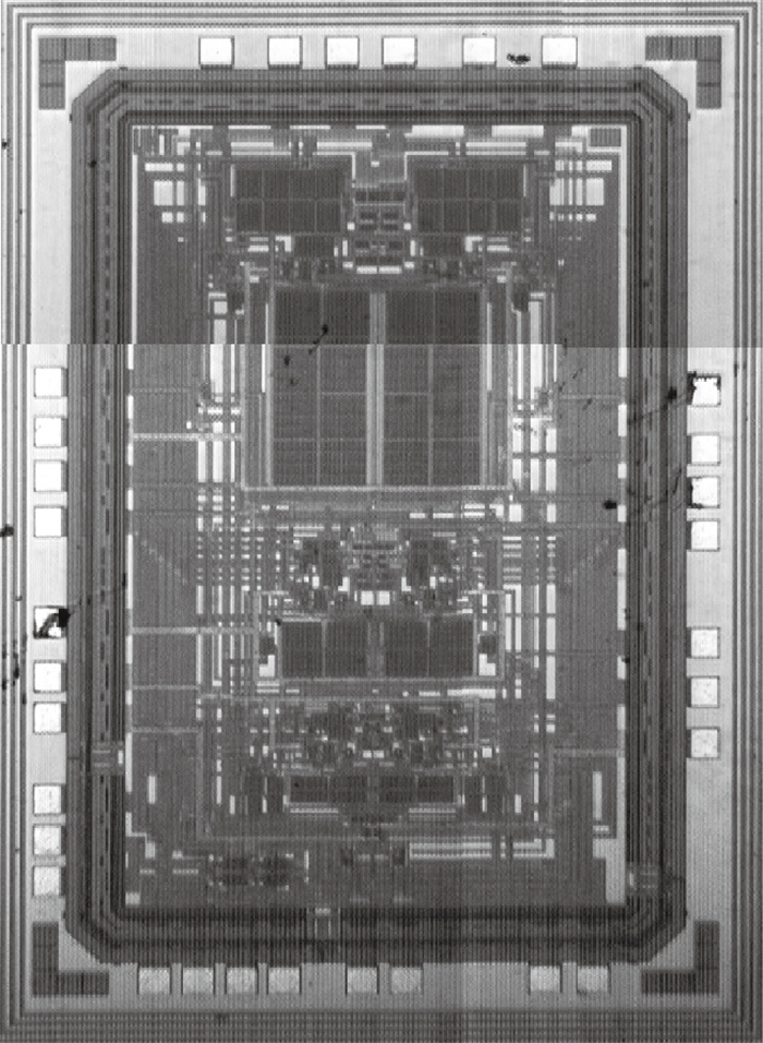
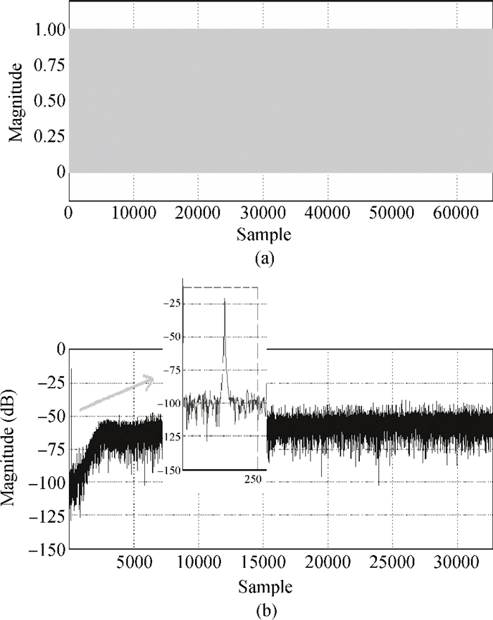
A low power and low voltage $\Sigma\Delta$ analog-to-digital modulator is realized with digital CMOS technology, which is due to full compensated depletion mode capacitors. Compared with mixed signal technology, this type of modulator is more compatible for pure digital applications. A pseudo-two-stage class-AB OTA is used in switched-capacitor integrators for low voltage and low power. The modulator is realized in standard SMIC 0.18 μm 1P6M digital CMOS technology. Measured results show that with 1.2 V supply voltage and a 6 MHz sample clock, the dynamic range of the modulator is 84 dB and the total power dissipation is 2460 μW.

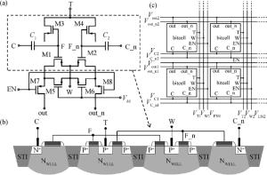
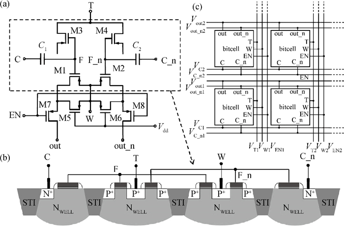
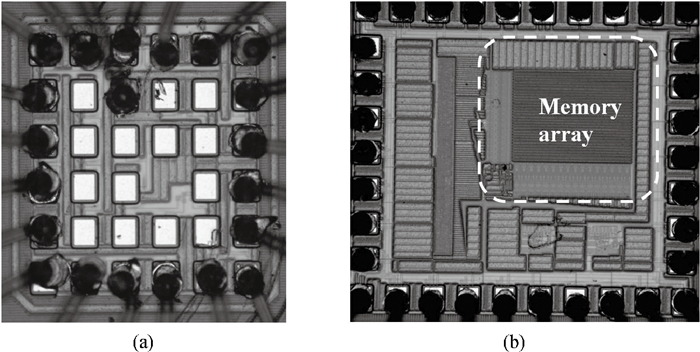
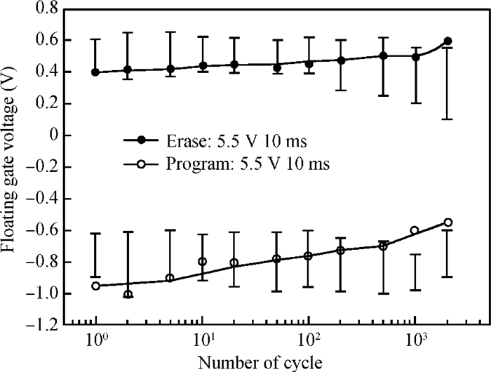
This paper presents an ultra-low-power area-efficient non-volatile memory (NVM) in a 0.18 μm single-poly standard CMOS process for passive radio frequency identification (RFID) tags. In the memory cell, a novel low-power operation method is proposed to realize bi-directional Fowler-Nordheim tunneling during write operation. Furthermore, the cell is designed with PMOS transistors and coupling capacitors to minimize its area. In order to improve its reliability, the cell consists of double floating gates to store the data, and the 1 kbit NVM was implemented in a 0.18 μm single-poly standard CMOS process. The area of the memory cell and 1 kbit memory array is 96 μm2 and 0.12 mm2, respectively. The measured results indicate that the program/erase voltage ranges from 5 to 6 V. The power consumption of the read/write operation is 0.19 μW/0.69 μW at a read/write rate of (268 kb/s)/(3.0 kb/s).
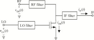
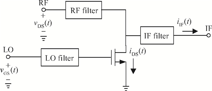
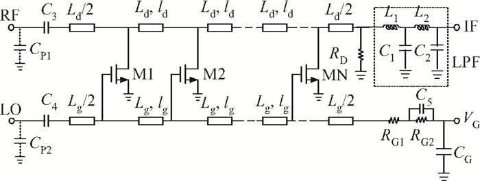
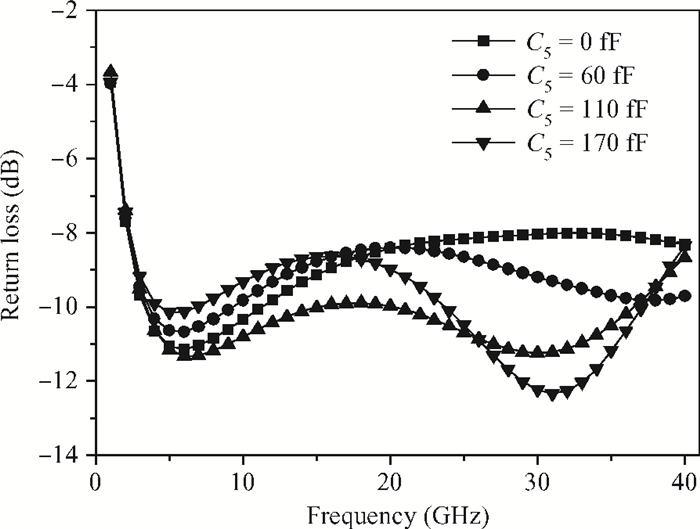
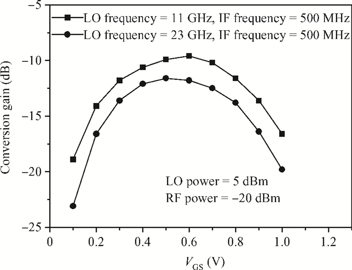
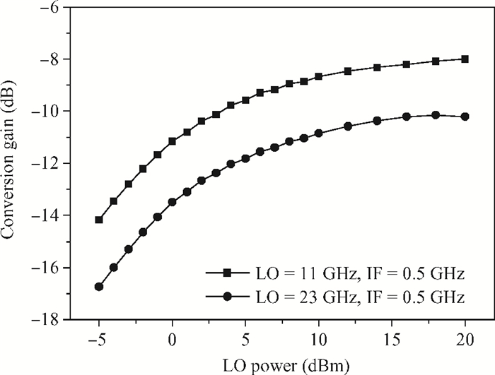
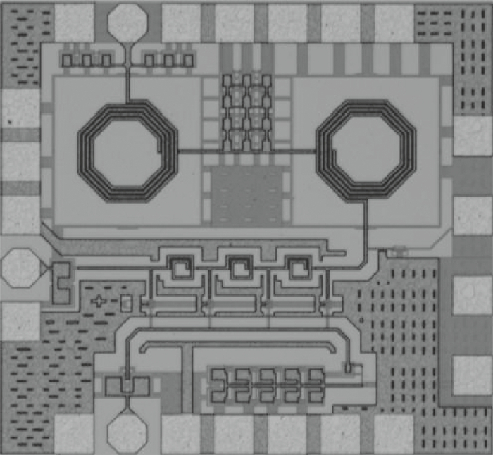
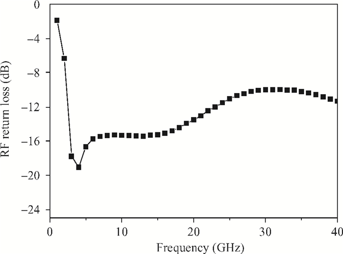
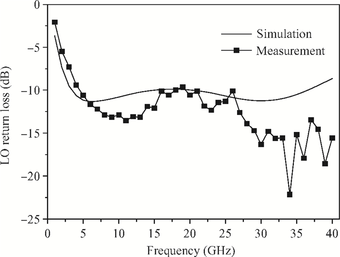
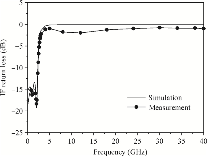
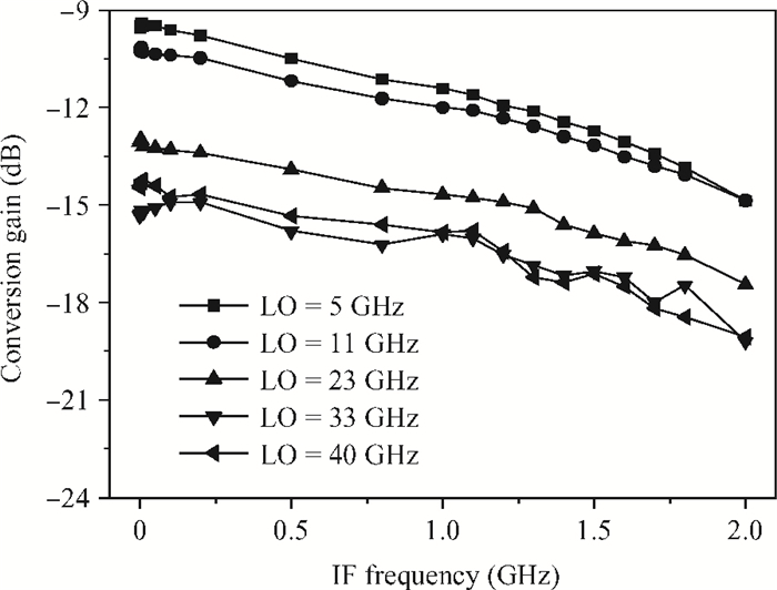
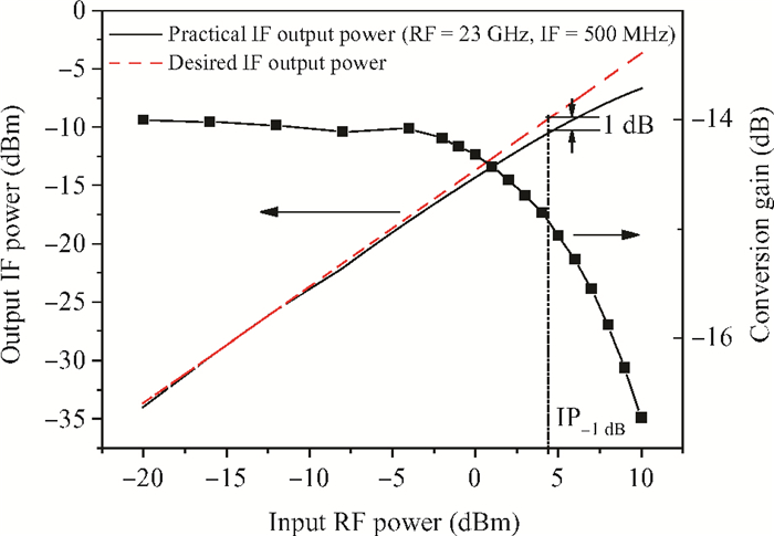
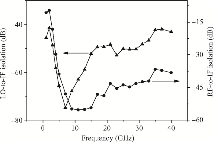
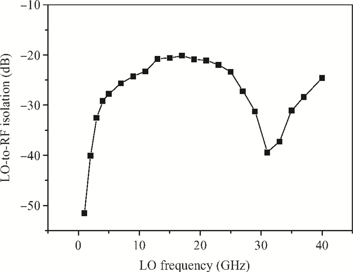
A broadband distributed passive gate-pumped mixer (DPGM) using standard 0.18 μm CMOS technology is presented. By employing distributed topology, the mixer can operate at a wide frequency range. In addition, a fourth-order low pass filter is applied to improve the port-to-port isolation. This paper also analyzes the impedance match and conversion loss of the mixer, which consumes zero dc power and exhibits a measured conversion loss of 9.4-17 dB from 3 to 40 GHz with a compact size of 0.78 mm2. The input referred 1 dB compression point is higher than 4 dBm at a fixed IF frequency of 500 MHz and RF frequency of 23 GHz, and the measured RF-to-LO, RF-to-IF and LO-to-IF isolations are better than 21, 38 and 45 dB, respectively. The mixer is suitable for WLAN, UWB, Wi-Max, automotive radar systems and other millimeter-wave radio applications.


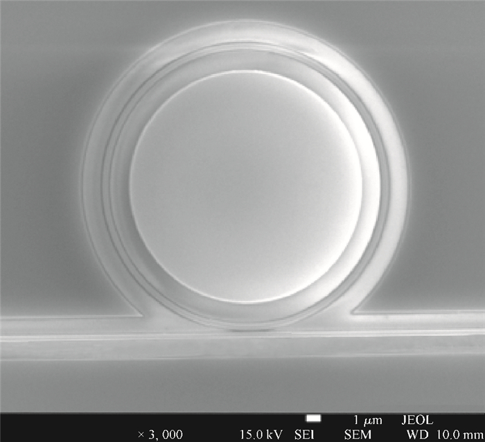
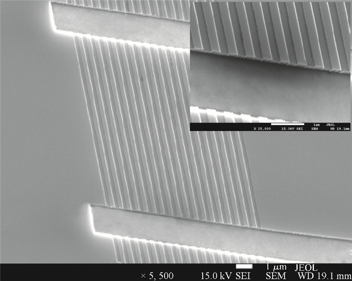
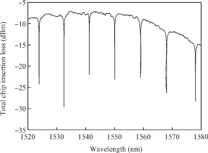
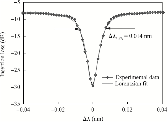
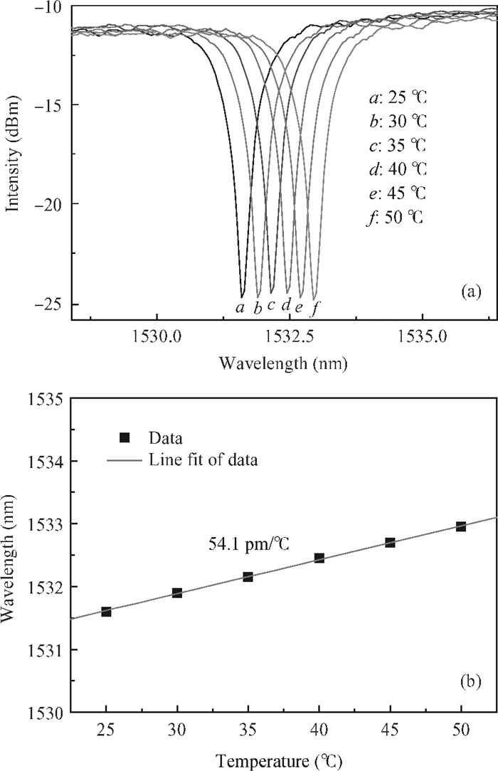
An ultra-small integrated photonic circuit has been proposed, which incorporates a high-quality-factor passive micro-ring resonator (MR) linked to a vertical grating coupler on a standard silicon-on-insulator (SOI) substrate. The experimental results demonstrate that the MR propagation loss is 0.532 dB/cm with a 10 μm radius ring resonator, the intrinsic quality factor is as high as 202.000, the waveguide grating wavelength response curve is a 1 dB bandwidth of 40 nm at 1540 nm telecommunication wavelengths, and the measured fiber-to-fiber coupling loss is 10 dB. Furthermore, the resonator wavelength temperature dependence of the 450 nm wide micro-ring resonator is 54.1 pm/℃. Such vertical grating coupler and low loss MR-integrated components greatly promote a key element in biosensors and high-speed interconnect communication applications.
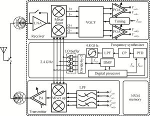
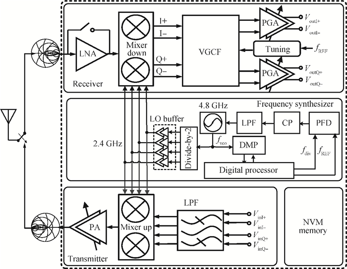
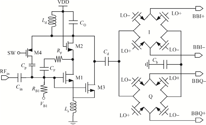
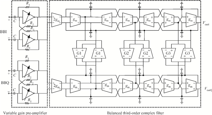
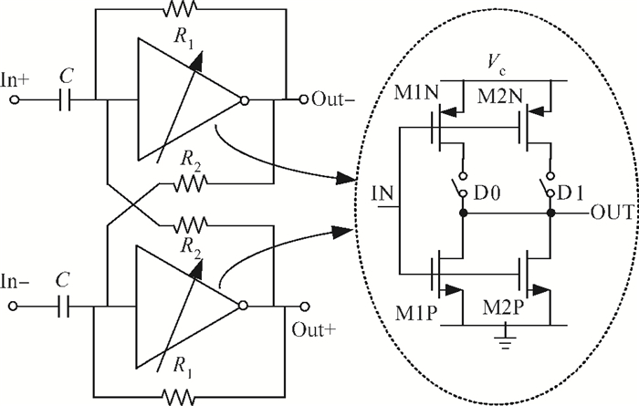
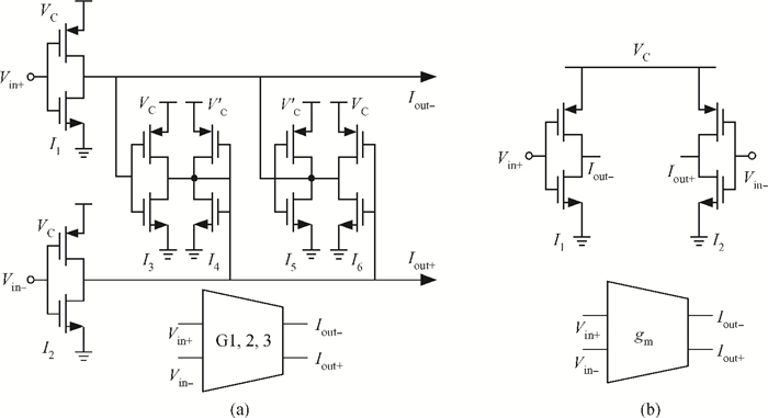
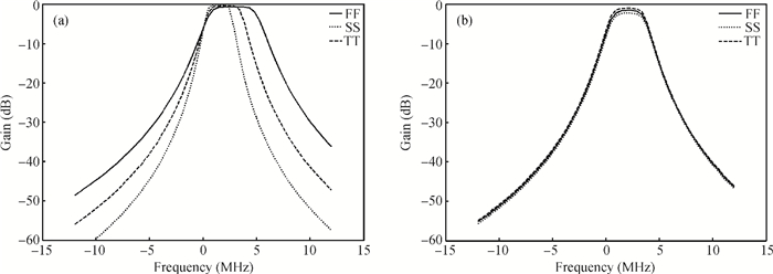
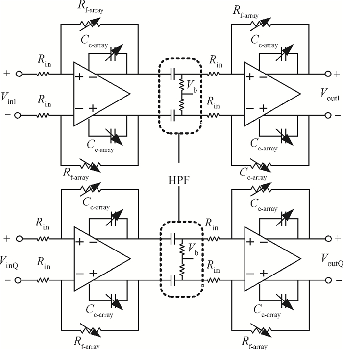
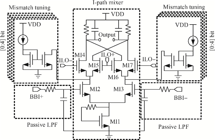
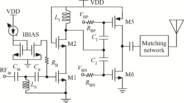
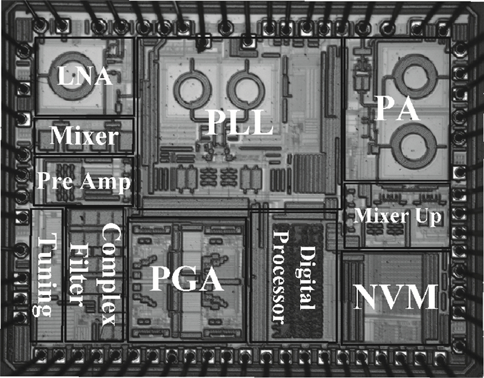
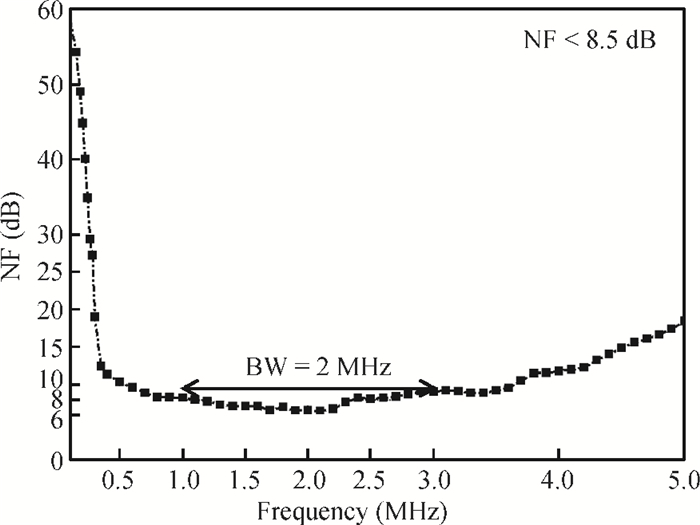
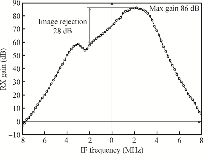
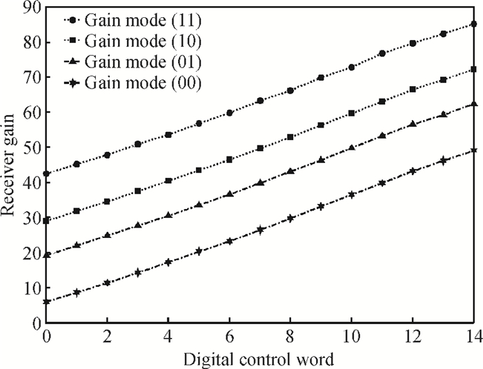
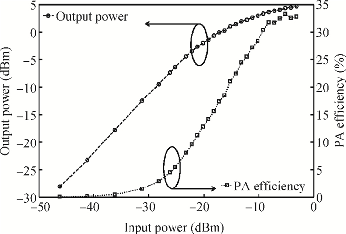
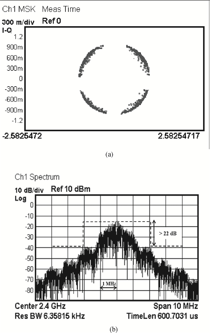
This paper presents a low power 2.4 GHz transceiver for ZigBee applications. This transceiver adopts low power system architecture with a low-IF receiver and a direct-conversion transmitter. The receiver consists of a new low noise amplifier (LNA) with a noise cancellation function, a new inverter-based variable gain complex filter (VGCF) for image rejection, a passive quadrature mixer, and a decibel linear programmable gain amplifier (PGA). The transmitter adopts a quadrature mixer and a class-B mode variable gain power amplifier (PA) to reduce power consumption. This transceiver is implemented in 0.18 μm CMOS technology. The receiver achieves -95 dBm of sensitivity, 28 dBc of image rejection, and -8 dBm of third-order input intercept point (ⅡP3). The transmitter can deliver a maximum of +3 dBm output power with PA efficiency of 30%. The whole chip area is less than 4.32 mm2. It only consumes 12.63 mW in receiving mode and 14.22 mW in transmitting mode, respectively.

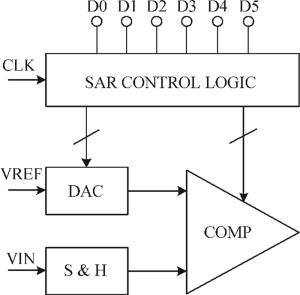
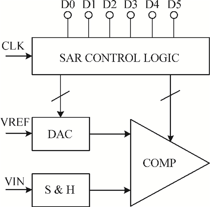
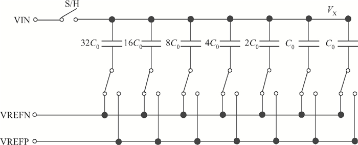
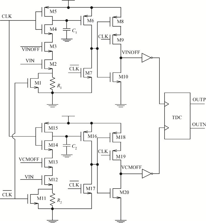
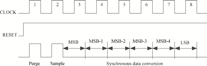
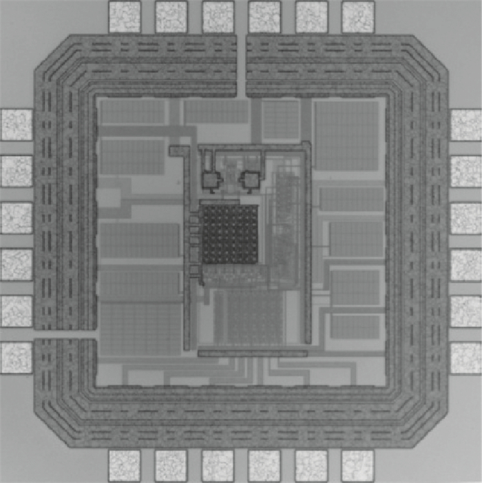
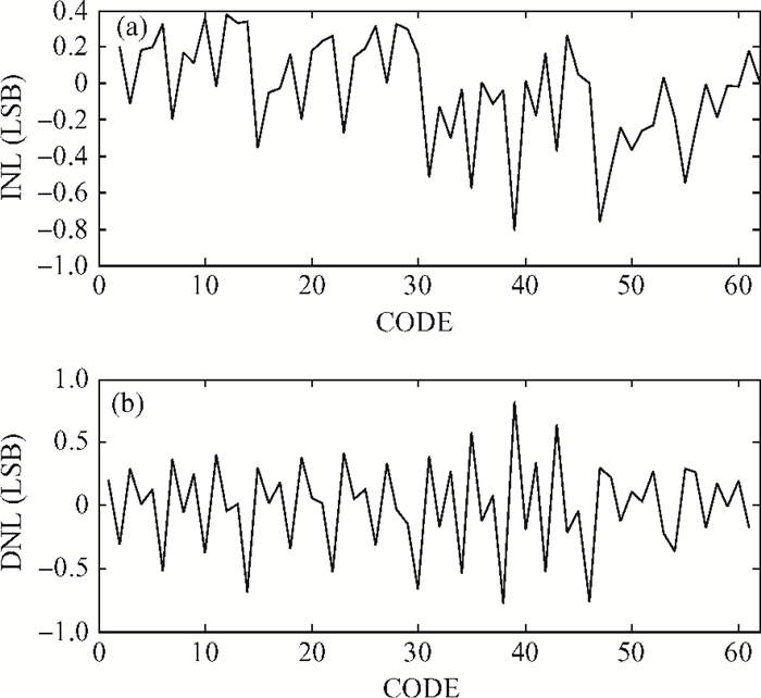
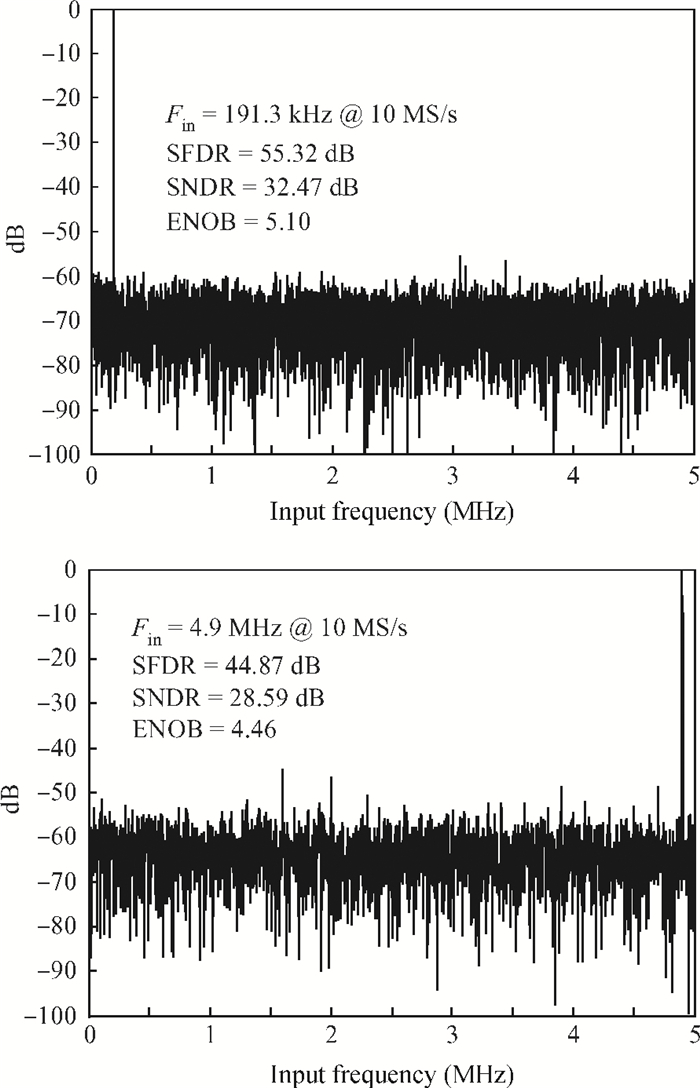
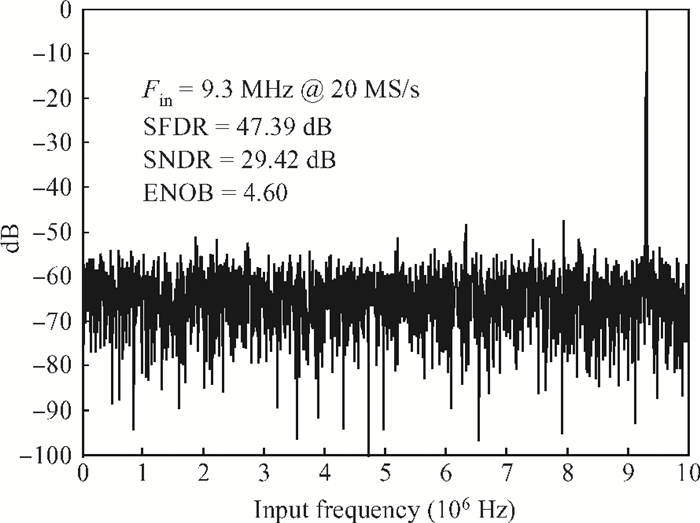
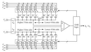
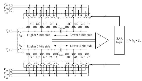
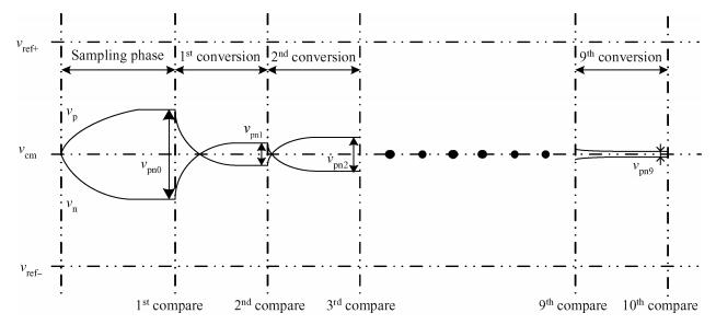
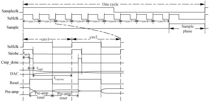
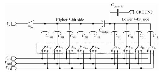
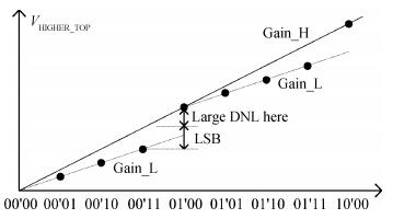
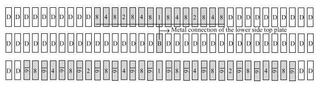
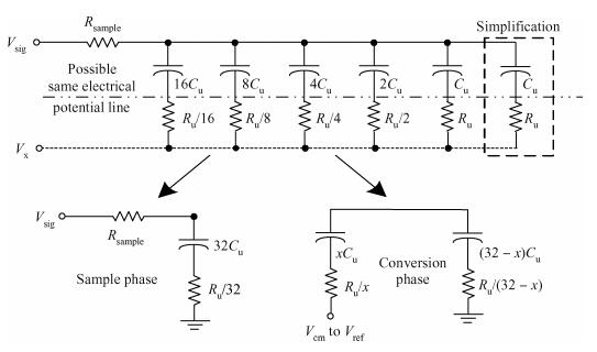
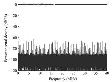
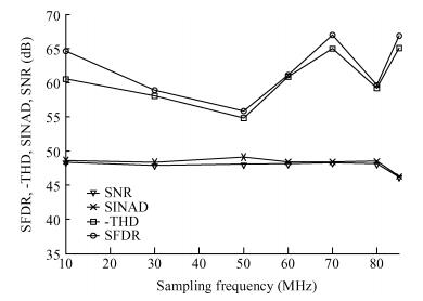
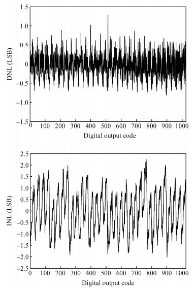
This paper presents a 6-bit 20-MS/s high spurious-free dynamic range (SFDR) and low power successive approximation register analog to digital converter (SAR ADC) for the radio-frequency (RF) transceiver front-end, especially for wireless sensor network (WSN) applications. This ADC adopts the modified common-centroid symmetry layout and the successive approximation register reset circuit to improve the linearity and dynamic range. Prototyped in a 0.18-μm 1P6M CMOS technology, the ADC performs a peak SFDR of 55.32 dB and effective number of bits (ENOB) of 5.1 bit for 10 MS/s. At the sample rate of 20 MS/s and the Nyquist input frequency, the 47.39-dB SFDR and 4.6-ENOB are achieved. The differential nonlinearity (DNL) is less than 0.83 LSB and the integral nonlinearity (INL) is less than 0.82 LSB. The experimental results indicate that this SAR ADC consumes a total of 522 μW power and occupies 0.98 mm2.


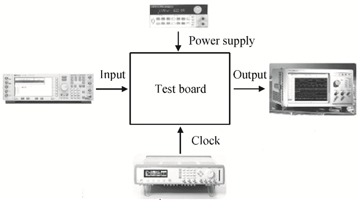
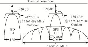
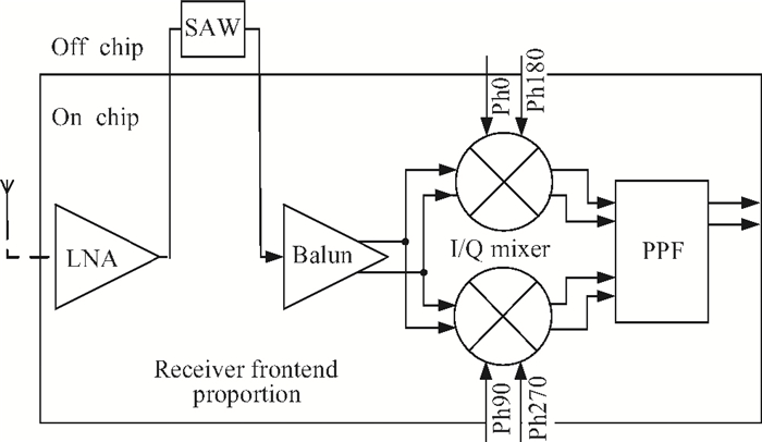
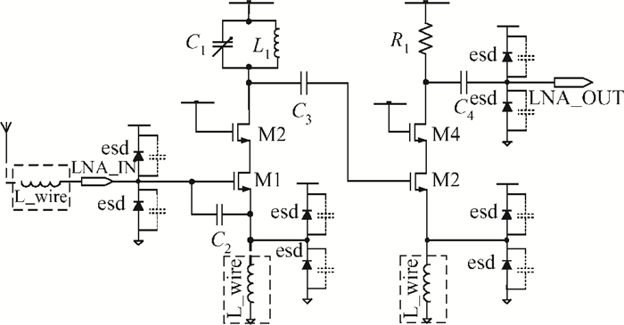
This paper introduces a fully integrated low power consumption radio receiver frontend circuit for a Compass (Beidou) and GPS dual mode dual channel system with 2.5 dB NF, 1.02 mm2 areas, and 8 mA of current in 0.18 μm TSMC CMOS process. Except for a few passive components for input matching, other components such as an off-chip low noise amplifier or a balun are not required. With a non-tunable passive image rejection filter, the receiver frontend can achieve around 60 dB gain and 34 dB image rejection.

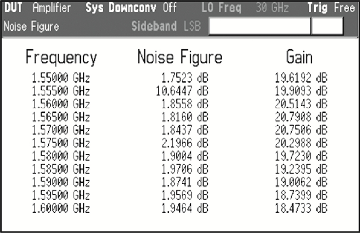

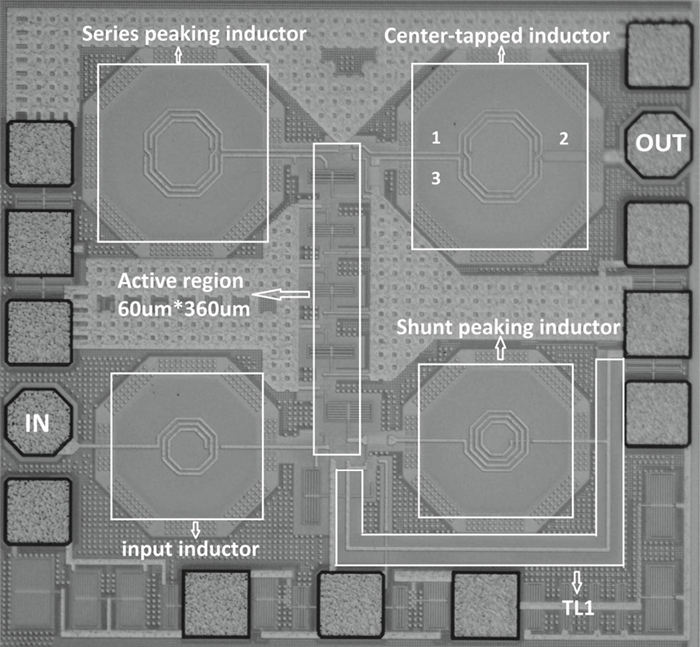
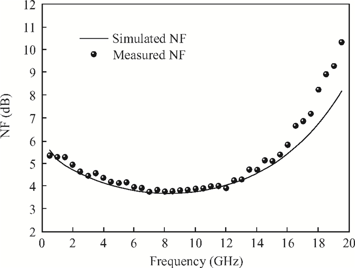
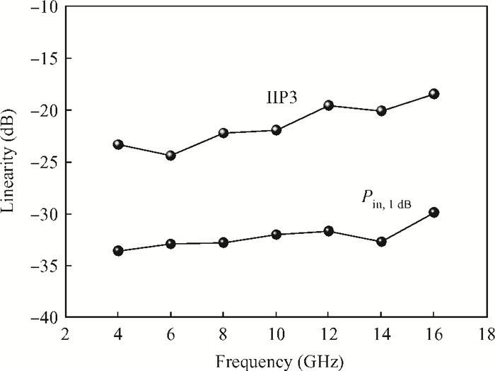
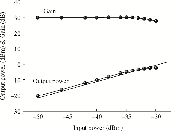
This paper presents a high-gain wideband low-noise IF amplifier aimed for the ALMA front end system using 90-nm LP CMOS technology. A topology of three optimized cascading stages is proposed to achieve a flat and wideband gain. Incorporating an input inductor and a gate-inductive gain-peaking inductor, the active shunt feedback technique is employed to extend the matching bandwidth and optimize the noise figure. The circuit achieves a flat gain of 30.5 dB with 3 dB bandwidth of 1-16 GHz and a minimum noise figure of 3.76 dB. Under 1.2 V supply voltage, the proposed IF amplifier consumes 42 mW DC power. The chip die including pads takes up 0.53 mm2, while the active area is only 0.022 mm2.


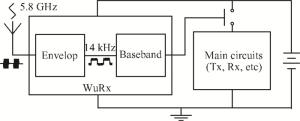
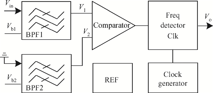
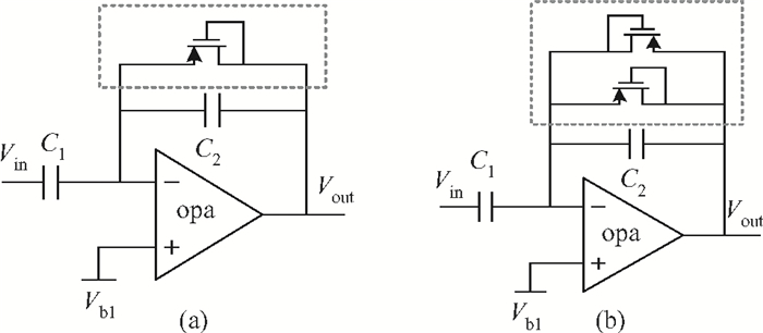
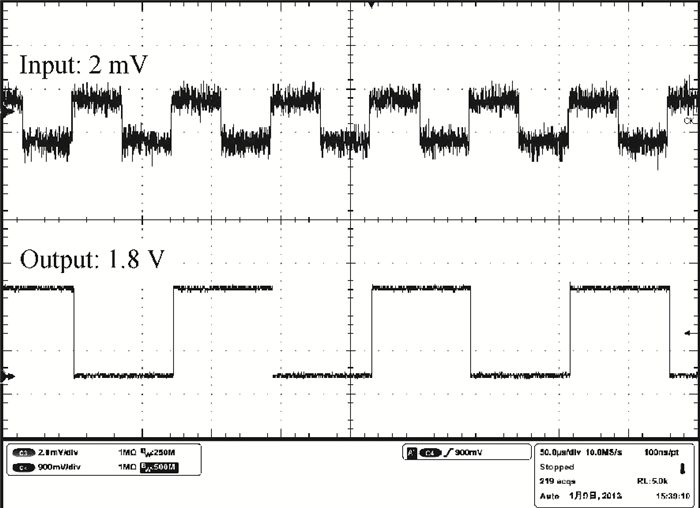
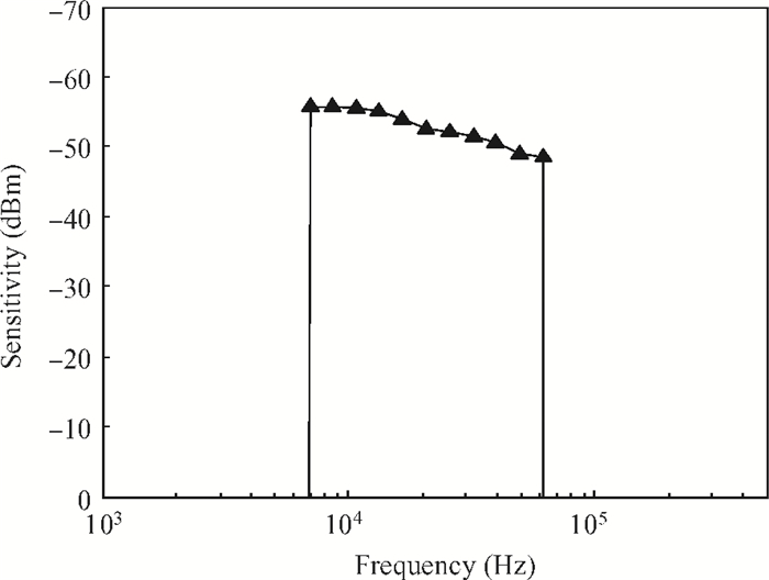
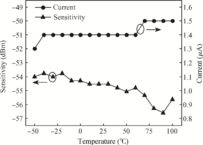
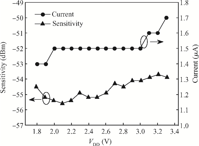
This paper proposes a baseband circuit for wake-up receivers with double-mode detection and enhanced sensitivity robustness for use in the electronic toll collection system. A double-mode detection method, including amplitude detection and frequency detection, is proposed to reject interference and reduce false wake-ups. An improved closed-loop band-pass filter and a DC offset cancellation technique are also newly introduced to enhance the sensitivity robustness. The circuit is fabricated in TSMC 0.18 μm 3.3 V CMOS technology with an area of 0.12 mm2. Measurement results show that the sensitivity is -54.5 dBm with only a ±0.95 dBm variation from the 1.8 to 3.3 V power supply, and that the temperature variation of the sensitivity is ±1.4 dBm from -50 to 100℃. The current consumption is 1.4 to 1.7 μA under a 1.8 to 3.3 V power supply.
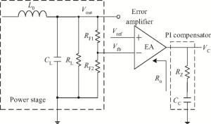
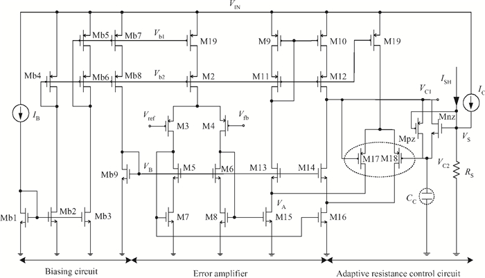
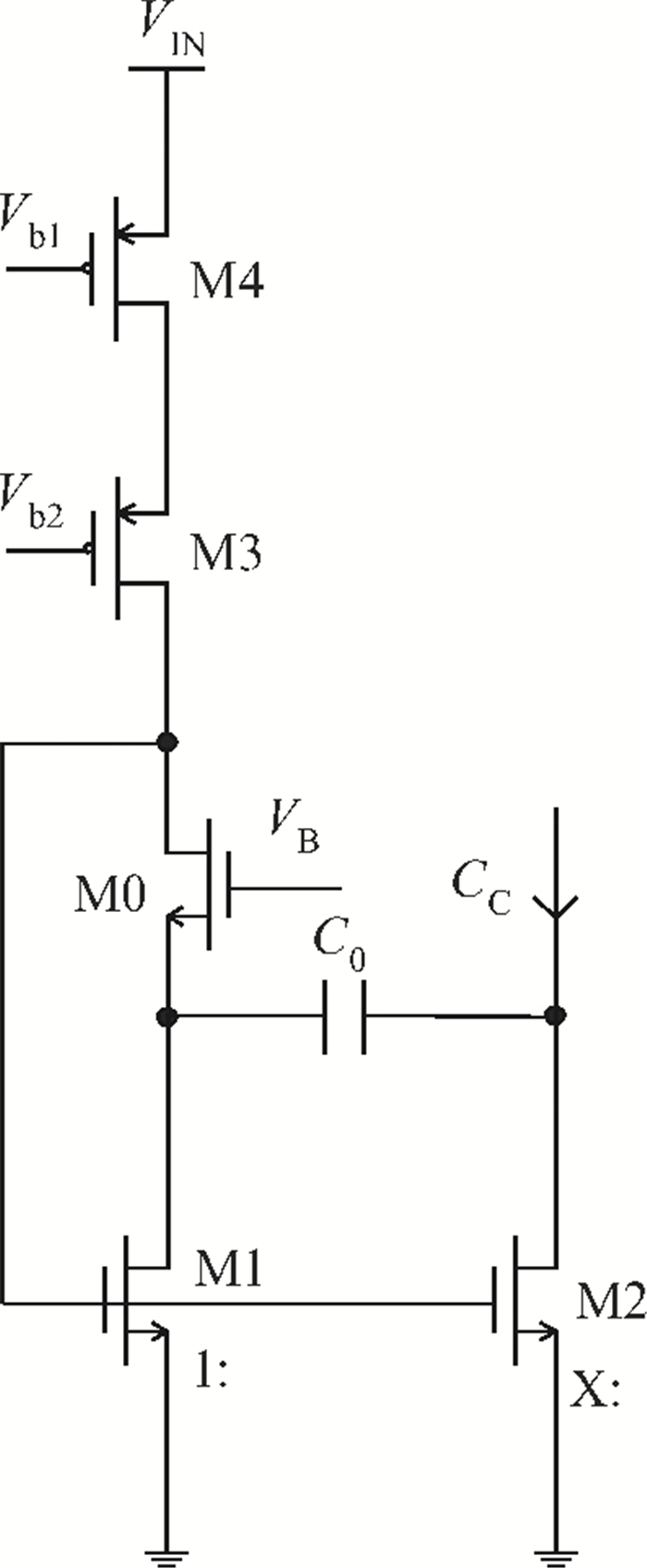
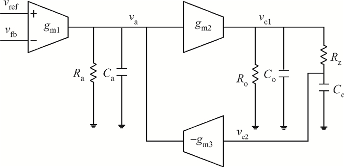
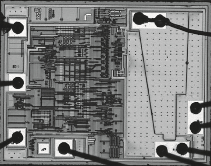
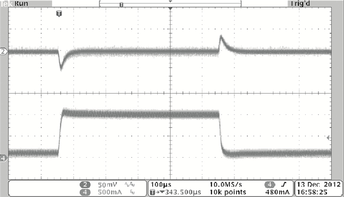
To achieve fast transient response for a DC-DC buck converter, an adaptive zero compensation circuit is presented. The compensation resistance is dynamically adjusted according to the different output load conditions, and achieves an adequate system phase margin under the different conditions. An improved capacitor multiplier circuit is adopted to realize the minimized compensation capacitance size. In addition, analysis of the small-signal model shows the correctness of the mechanism of the proposed adaptive zero compensation technique. A current-mode DC-DC buck converter with the proposed structure has been implemented in a 0.35 μm CMOS process, and the die size is only 800×1040 μm2. The experimental results show that the transient undershoot/overshoot voltage and the recovery times do not exceed 40 mV and 30 μs for a load current variation from 100 mA to 1 A.
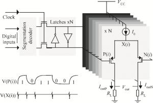
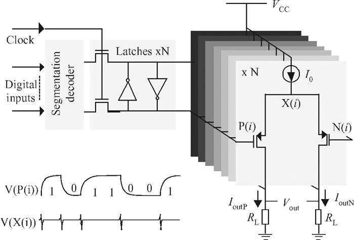
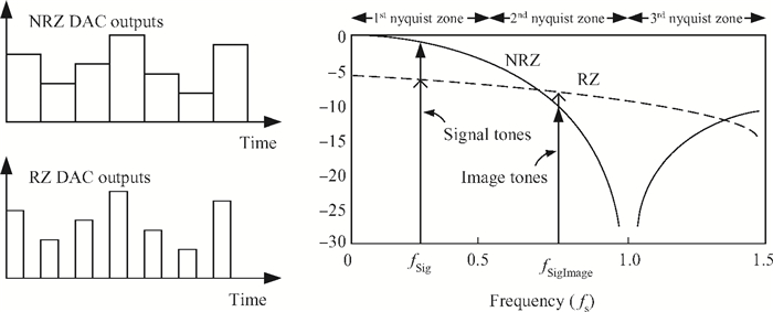
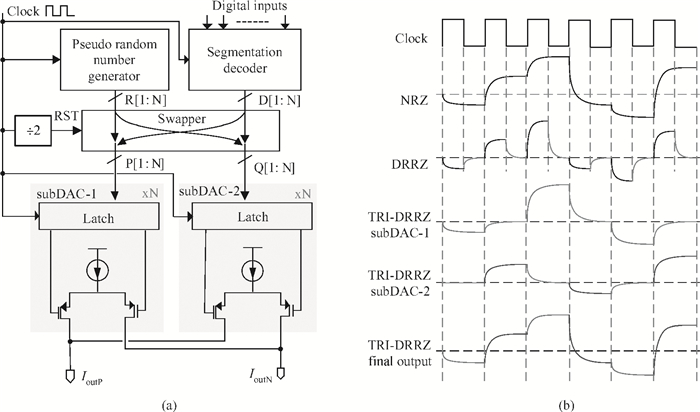
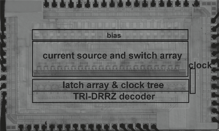
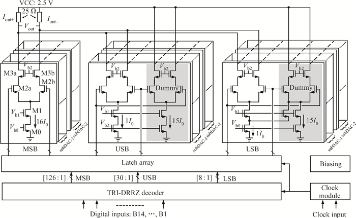
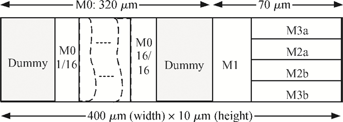
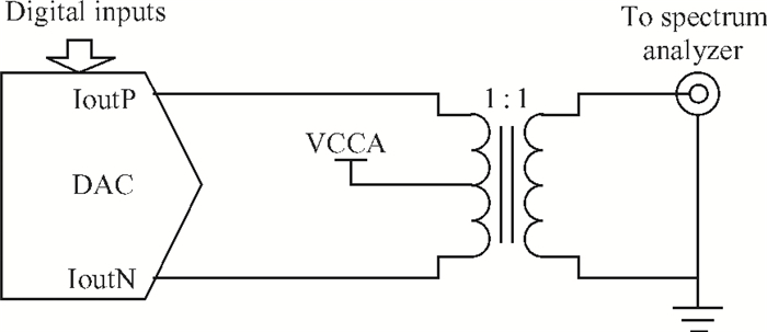
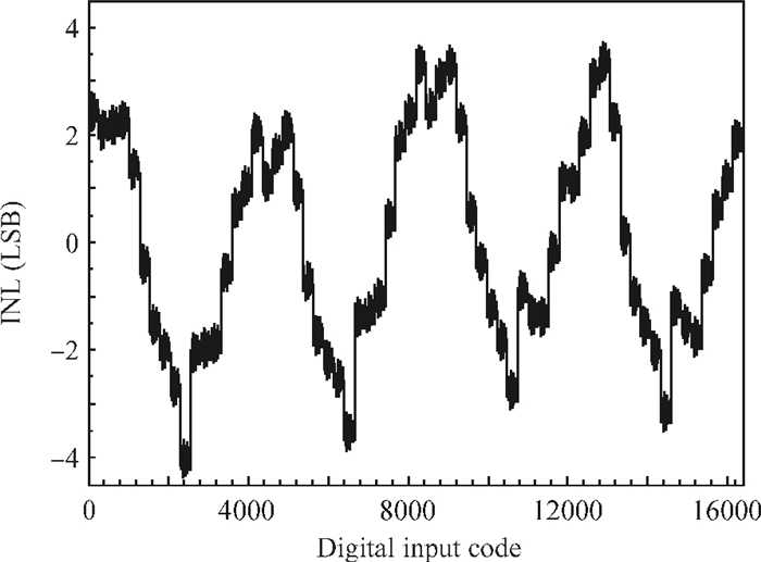
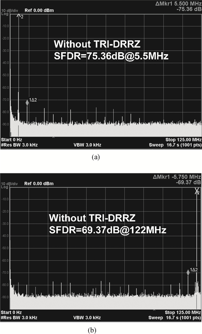
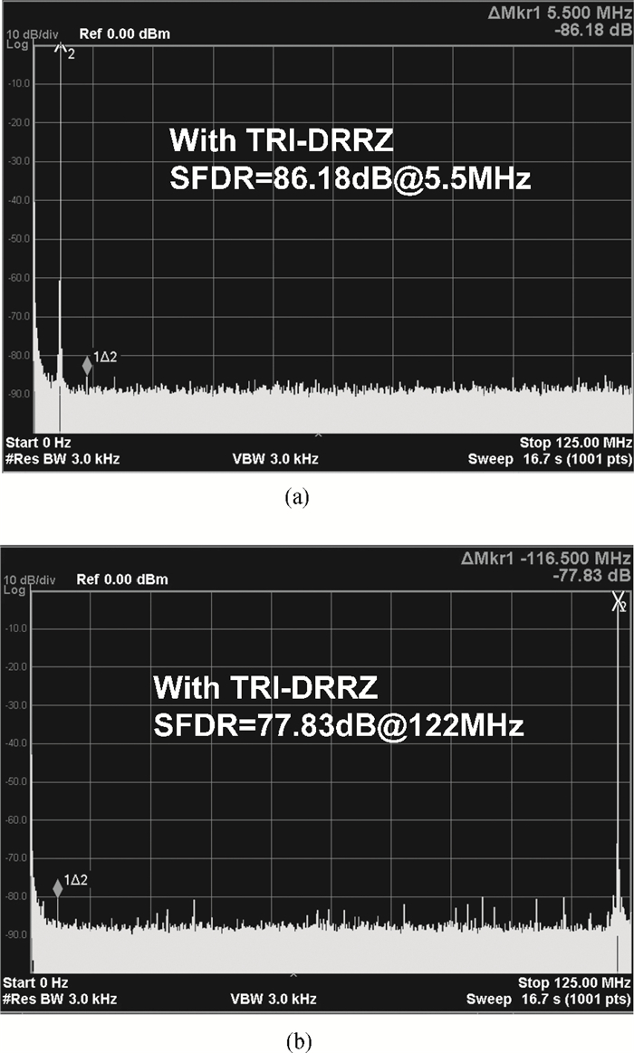
A 14-bit 250-MS/s current-steering digital-to-analog converter (DAC) was fabricated in a 0.13 μm CMOS process. In conventional high-speed current-steering DACs, the spurious-free dynamic range (SFDR) is limited by nonlinear distortions in the code-dependent switching glitches. In this paper, the bottleneck is mitigated by the time-relaxed interleaving digital-random-return-to-zero (TRI-DRRZ). Under 250-MS/s sampling rate, the measured SFDR is 86.2 dB at 5.5-MHz signal frequency and 77.8 dB up to 122 MHz. The DAC occupies an active area of 1.58 mm2 and consumes 226 mW from a mixed power supply of 1.2/2.5 V.


This paper presents a 10-bit 80-MS/s successive approximation register (SAR) analog-to-digital converter (ADC) suitable for integration in a system on a chip (SoC). By using the top-plate-sample switching scheme and a split capacitive array structure, the total capacitance is dramatically reduced which leads to low power and high speed. Since the split structure makes the capacitive array highly sensitive to parasitic capacitance, a three-row layout method is applied to the layout design. To overcome the charge leakage in the nanometer process, a special input stage is proposed in the comparator. As 80 MS/s sampling rate for a 10-bit SAR ADC results in around 1 GHz logic control clock, and a tunable clock generator is implemented. The prototype was fabricated in 65 nm 1P9M (one-poly-nine-metal) GP (general purpose) CMOS technology. Measurement results show a peak signal-to-noise and distortion ratio (SINAD) of 48.3 dB and 1.6 mW total power consumption with a figure of merit (FOM) of 94.8 fJ/conversion-step.

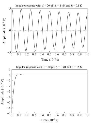
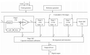
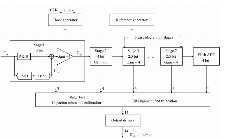
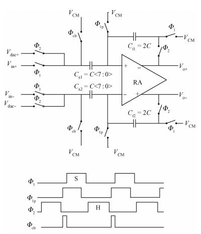
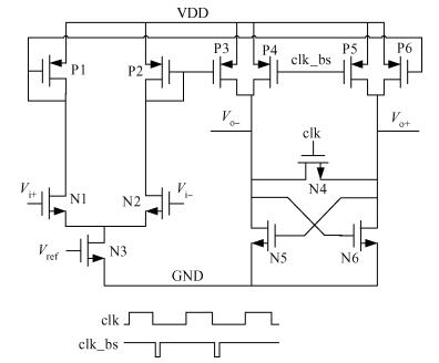
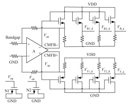
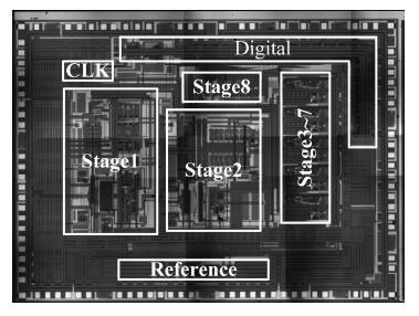
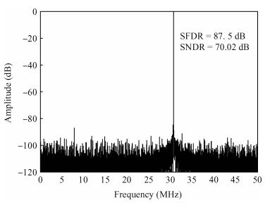
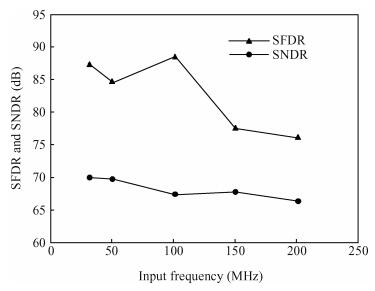
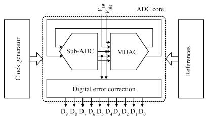
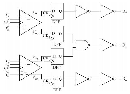
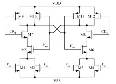
This paper demonstrates a 14-bit 100-MS/s pipelined analog-to-digital converter (ADC) in 0.18 μm CMOS process with a 1.8 V supply voltage. A fast foreground digital calibration mechanism is employed to correct capacitor mismatches. The ADC implements an SHA-less 3-bit front-end to reduce the size of the sampled capacitor. The presented ADC achieves a 70.02 dB signal-to-noise distortion ratio (SNDR) and an 87.5 dB spurious-free dynamic range (SFDR) with a 30.7 MHz input signal, while maintaining over 66 dB SNDR and 76 dB SFDR up to 200 MHz input. The power consumption is 543 mW and a total die area of 3×4 mm2 is occupied.


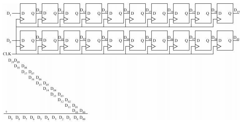
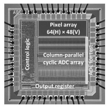
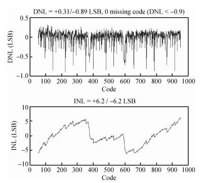
This paper presents a high-speed column-parallel cyclic analog-to-digital converter (ADC) for a CMOS image sensor. A correlated double sampling (CDS) circuit is integrated in the ADC, which avoids a stand-alone CDS circuit block. An offset cancellation technique is also introduced, which reduces the column fixed-pattern noise (FPN) effectively. One single channel ADC with an area less than 0.02 mm2 was implemented in a 0.13 μm CMOS image sensor process. The resolution of the proposed ADC is 10-bit, and the conversion rate is 1.6 MS/s. The measured differential nonlinearity and integral nonlinearity are 0.89 LSB and 6.2 LSB together with CDS, respectively. The power consumption from 3.3 V supply is only 0.66 mW. An array of 48 10-bit column-parallel cyclic ADCs was integrated into an array of CMOS image sensor pixels. The measured results indicated that the ADC circuit is suitable for high-speed CMOS image sensors.

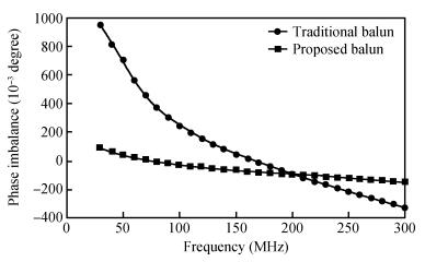
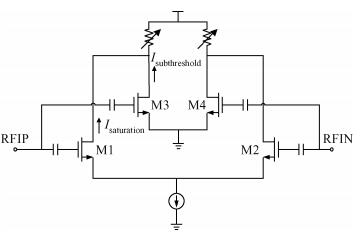
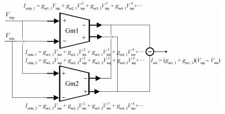
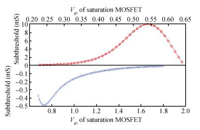
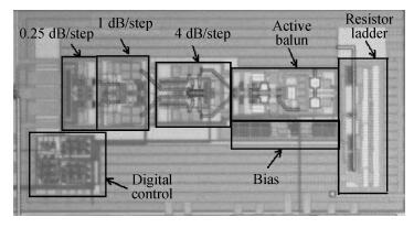
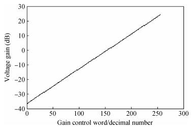
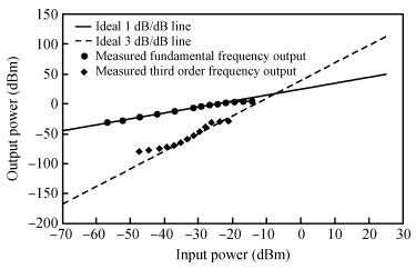
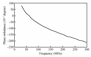
This paper presents a VHF (30-300 MHz) RF programmable gain amplifier (PGA) with an adaptive phase correction technique. The proposed technique effectively mitigates phase errors over the VHF band, and the RFPGA as a whole satisfies all the specifications of the China mobile multimedia broadcasting VHF band applications. The RFPGA is implemented with a TSMC 0.25 μm CMOS process. Measurement results reveal a gain range of around 61 dB, an ⅡP3 of -7 dBm at maximum gain, a power consumption of 10.2 mA at maximum gain, and a phase imbalance of less than 0.3 degrees.

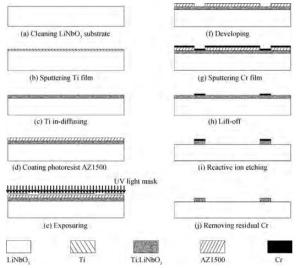
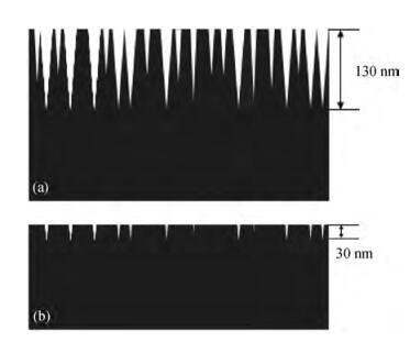
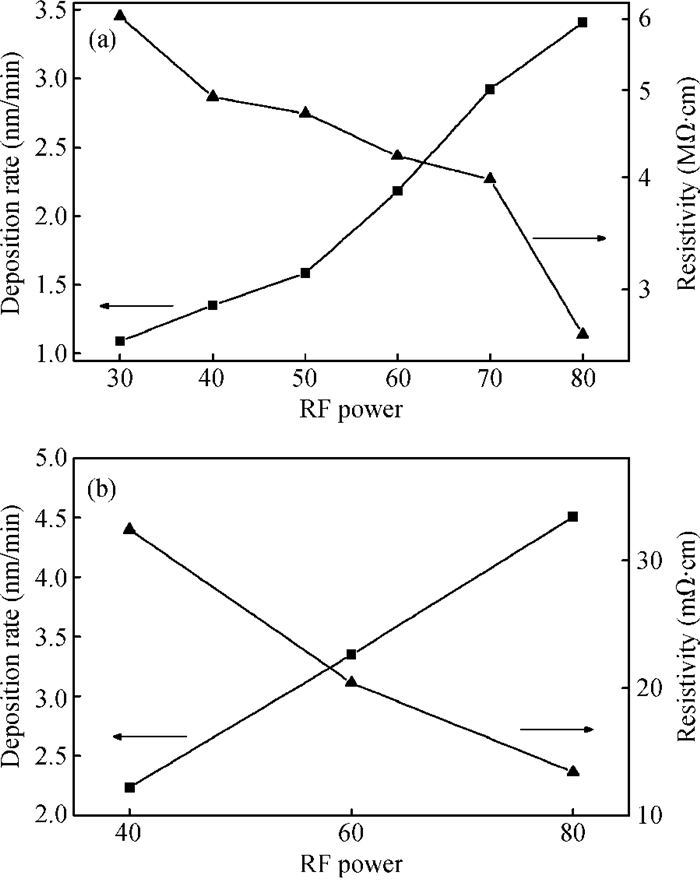
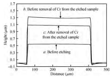
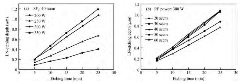
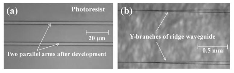
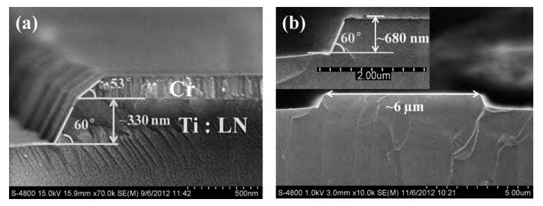
Reactive ion etching (RIE) of LiNbO3 (LN) in SF6 plasma atmosphere was studied for optimizing the preparation conditions for LN ridge waveguides. The samples to be etched are Ti-diffused LN slab waveguides overlaid with a chromium film mask that has a Mach-Zehnder interferometer (MZI) array pattern. The experimental results indicate that the LN-etching rate (RLN) and the Cr-etching rate (RCr) as well as the rate ratio RLN/RCr increase with either increasing the radio-frequency (RF) power at a given SF6 flow rate or increasing the SF6 flow rate at a fixed RF power. The maximum values of RLN=43.2 nm/min and RLN/RCr=3.27 were achieved with 300 W RF power and 40 sccm SF6 flow. When the SF6 flow rate exceeds 40 sccm, an increase in the flow rate causes the etching rates and the rate ratio to decrease. The scanning electron microscope images of the LN ridge prepared after ~ 20 min etching show that the ridge height is 680 nm and the sidewall slope angle is about 60°.

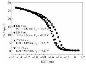
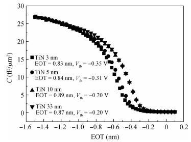
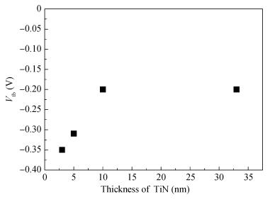
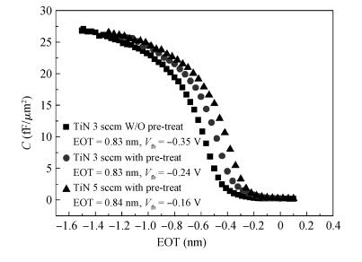
It is important to find a way to modulate the work function of TiN metal gate towards the valence band edge of Si, which can meet the lower threshold voltage requirement of p-type metal-oxide-semiconductor (MOS) transistor. In this work, effects of TiN thickness, post-deposition annealing (PDA), oxygen incorporation and N concentration variation on the work function of TiN metal gate in MOS structures are systematically investigated. It can be found that the work function positively shifts at the initial stage as the thickness of the TiN layer increases and stabilizes at such a thickness. PDA at N2 ambience with a trace of O2 can also cause a positive shift in the work function of TiN metal gate. The same tendency can be observed when oxygen is incorporated into TiN. Finally, increasing the N concentration in TiN can also positively shift the work function. All these measures are effective in modulating the TiN metal gate so that it is more suitable for PMOS application.

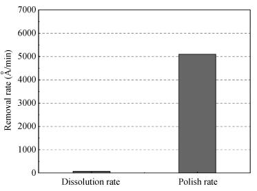
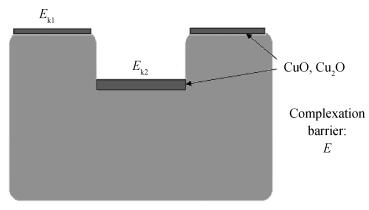
The planarization mechanism of alkaline copper slurry is studied in the chemical mechanical polishing (CMP) process from the perspective of chemical mechanical kinetics. Different from the international dominant acidic copper slurry, the copper slurry used in this research adopted the way of alkaline technology based on complexation. According to the passivation property of copper in alkaline conditions, the protection of copper film at the concave position on a copper pattern wafer surface can be achieved without the corrosion inhibitors such as benzotriazole (BTA), by which the problems caused by BTA can be avoided. Through the experiments and theories research, the chemical mechanical kinetics theory of copper removal in alkaline CMP conditions was proposed. Based on the chemical mechanical kinetics theory, the planarization mechanism of alkaline copper slurry was established. In alkaline CMP conditions, the complexation reaction between chelating agent and copper ions needs to break through the reaction barrier. The kinetic energy at the concave position should be lower than the complexation reaction barrier, which is the key to achieve planarization.
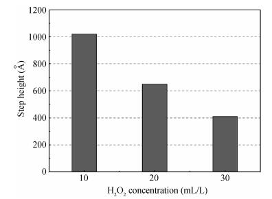
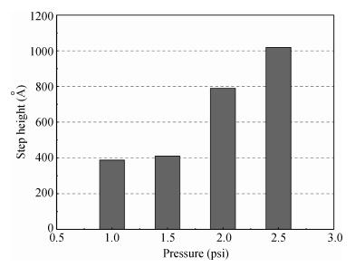
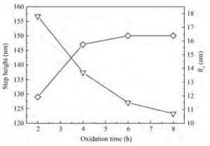
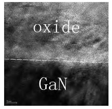
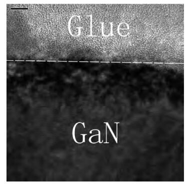
A novel wet etching method for AlGaN/GaN heterojunction structures is proposed using thermal oxidation followed by wet etching in KOH solution. It is found that an AlGaN/GaN heterostructure after high temperature oxidation above 700℃ could be etched off in a homothermal (70℃) KOH solution while the KOH solution had no etching effects on the region of the AlGaN/GaN heterostructure protected by a SiO2 layer during the oxidation process. A groove structure with 150 nm step depth on an AlGaN/GaN heterostructure was formed after 8 h thermal oxidation at 900℃ followed by 30 min treatment in 70℃ KOH solution. As the oxidation time increases, the etching depth approaches saturation and the roughness of the etched surface becomes much better. The physical mechanism of this phenomenon is also discussed.


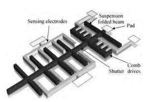
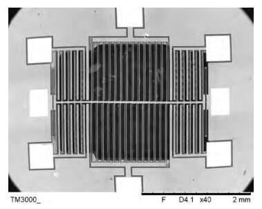
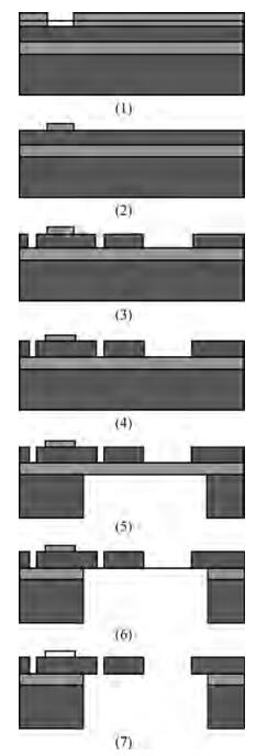
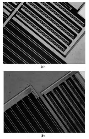
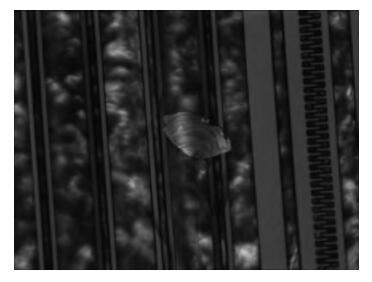
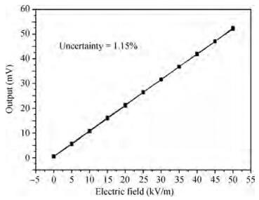
This paper presents a new fabrication process for the SOI-based novel miniature electric field sensor. This new process uses polyimide film to release the SiO2 layer. Compared with the CO2 critical point release method, it significantly improves the device surface cleanliness and shortens the process flow. The impurity on the base layer is analyzed. The problem of peak and butterfly-type contamination occurring on the base layer of the SOI wafer during the DRIE process is discussed and solved by thickening the photoresist layer and coating with polyimide film twice. This new process could fabricate MEMS sensors and actuators such as SOI-based electric field sensors, gyroscopes, and micro mirrors and can be an alternative fabrication process compared to commercial SOIMUMPS fabrication processes.