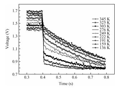
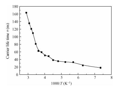
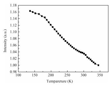
The influence of temperature on the intensity of light emitted by as well as the carrier life time τ of a standard AlGaAs based light emitting diode has been investigated in the temperature range from 345 to 136 K. The open-circuit voltage decay (OCVD) technique has been used for measured the carrier lifetime. Our experimental results reveal a 16% average increase in intensity and a 163.482-19.765 ns variation in carrier lifetime in the above temperature range. Further, theoretical and experimental analysis show that for negligible carrier density the intensity is inversely proportional to carrier lifetime for this sample.
Issue Browser
Volume 34, Issue 9,
Sep 2013

J. Semicond.
2013, 34(9): 092002 doi: 10.1088/1674-4926/34/9/092002
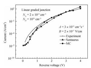
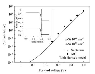
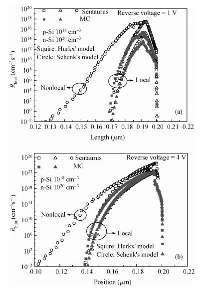
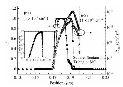
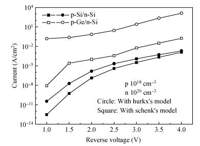
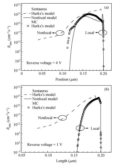
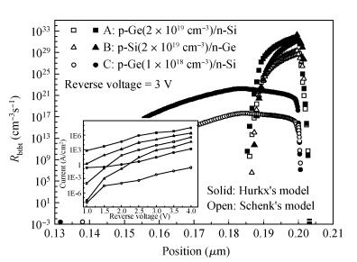
We compared several different band-to-band tunneling (BTBT) models with both Sentaurus and the two-dimensional full-band Monte Carlo simulator in Si homo-junctions and Si-Ge hetero-junctions. It was shown that in Si homo-junctions, different models could achieve similar results. However, in the Si-Ge hetero-junctions, there were significant differences among these models at high reverse biases (over 2 V). Compared to the nonlocal model, the local models in Sentaurus underrated the BTBT rate distinctly, and the Monte Carlo method was shown to give a better approximation. Additionally, it was found that in the Si region near the interface of the Si-Ge hetero-junctions, the direct tunneling rates increased largely due to the interaction of the band structures of Si and Ge.


J. Semicond.
2013, 34(9): 093001 doi: 10.1088/1674-4926/34/9/093001

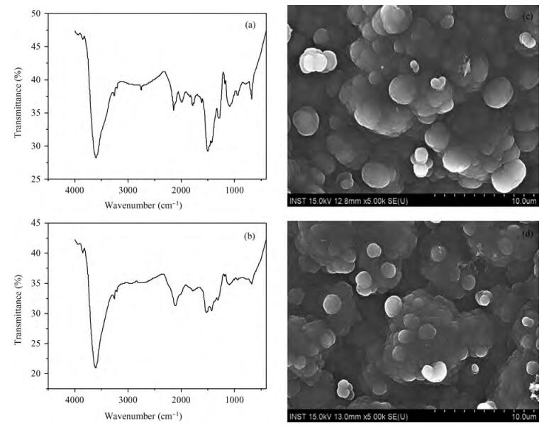
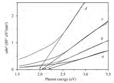
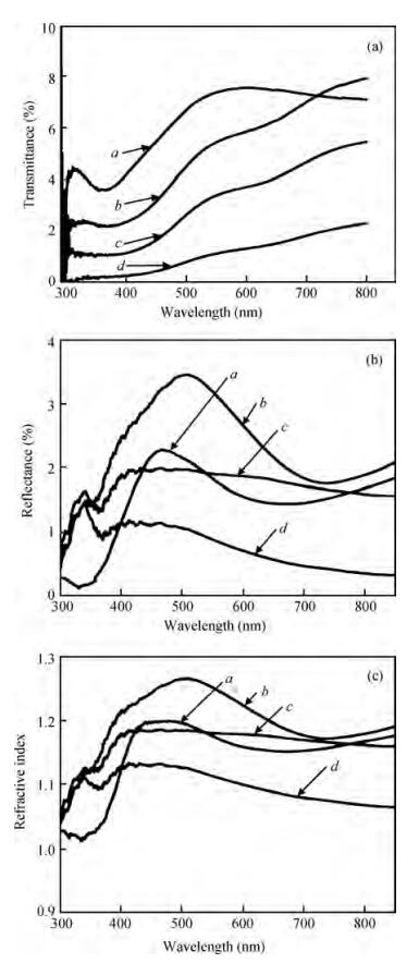
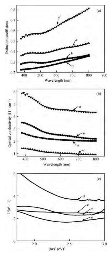
The optical properties of polypyrrole (Ppy) thin films upon 2 MeV electron beam irradiation changes with different doses. The induced changes in the optical properties for Ppy thin films were studied in the visible range 300 to 800 nm at room temperature. The optical band gap of the pristine Ppy was found to be 2.19 eV and it decreases up to 1.97 eV for a 50 kGy dose of 2 MeV electron beam. The refractive index dispersion of the samples obeys the single oscillator model. The obtained results suggest that electron beam irradiation changes the optical parameters of Ppy thin films.

J. Semicond.
2013, 34(9): 093002 doi: 10.1088/1674-4926/34/9/093002
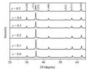
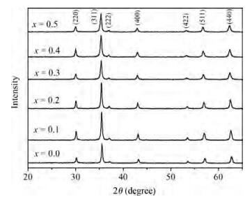
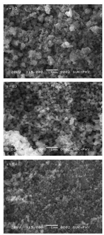
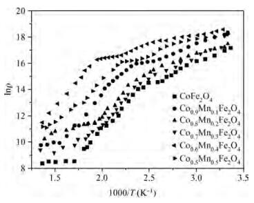
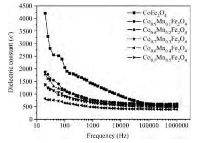
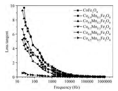
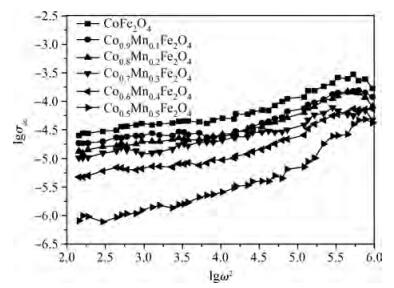
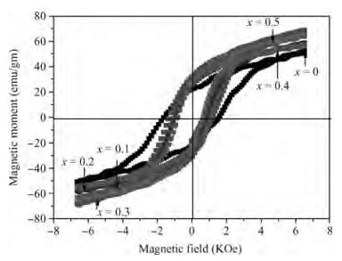
The Co1-xMnxFe2O4 (0 ≤ x ≤ qslant 0.5) ferrite system is synthesized by using an auto combustion technique using metal nitrates. The influence of Mn substitution on the structural, electrical, impedance and magnetic properties of cobalt ferrite is reported. X-ray diffraction patterns of the prepared samples confirm that the Bragg's peak belongs to a spinel cubic crystal structure. The lattice constant of cobalt ferrite increases with the increase in Mn content. The microstructural study is carried out by using the SEM technique and the average grain size continues to increase with increasing manganese content. AC conductivity analysis suggests that the conduction is due to small polaron hopping. DC electrical resistivity decreases with increasing temperature for a Co1-xMnxFe2O4 system showing semiconducting behavior. The activation energy is found to be higher in the paramagnetic region than the ferromagnetic region. Curie temperature decreases with Mn substitution in the host ferrite system. Dielectric dispersion having Maxwell-Wagner-type interfacial polarization has been observed for cobalt ferrite samples. Magnetic properties have been studied by measuring M-H plots. The saturation and remanent magnetization increases with Mn substitution.
J. Semicond.
2013, 34(9): 093003 doi: 10.1088/1674-4926/34/9/093003
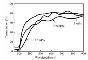
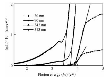
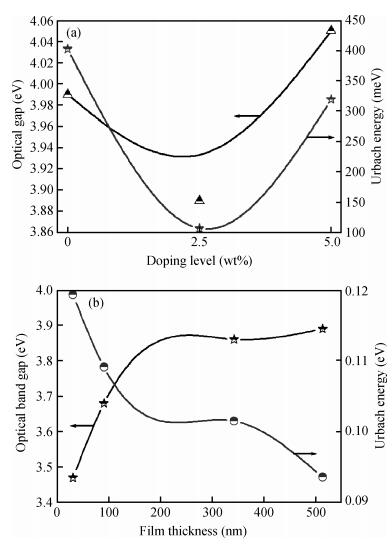
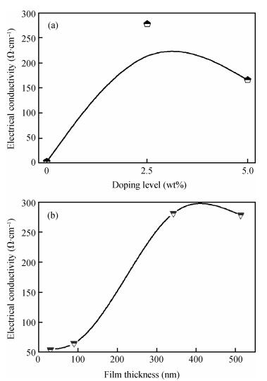
This paper reports on the effects of film thickness and doping content on the optical and electrical properties of fluorine-doped tin oxide. Tin (Ⅱ) chloride dehydrate, ammonium fluoride dehydrate, ethanol and HCl were used as the starting materials, dopant source, solvent and stabilizer, respectively. The doped films were deposited on a glass substrate at different concentrations varying between 0 and 5 wt% using an ultrasonic spray technique. The SnO2:F thin films were deposited at a 350℃ pending time (5, 15, 60 and 90 s). The average transmission was about 80%, and the films were thus transparent in the visible region. The optical energy gap of the doped films with 2.5 wt% F was found to increase from 3.47 to 3.89 eV with increasing film thickness, and increased after doping at 5 wt%. The decrease in the Urbach energy of the SnO2:F thin films indicated a decrease in the defects. The increase in the electrical conductivity of the films reached maximum values of 278.9 and 281.9 (Ω· cm)-1 for 2.5 and 5 wt% F, respectively, indicating that the films exhibited an n-type semiconducting nature. A systematic study on the influence of film thickness and doping content on the properties of SnO2:F thin films deposited by ultrasonic spray was reported.


J. Semicond.
2013, 34(9): 093004 doi: 10.1088/1674-4926/34/9/093004

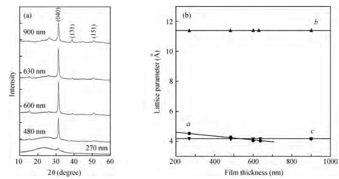
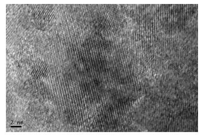
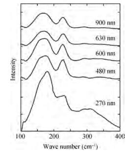
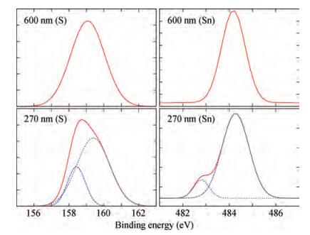
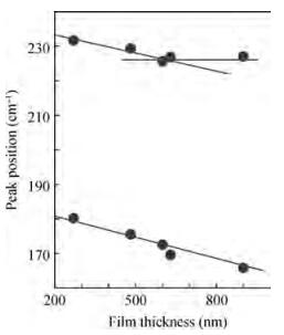
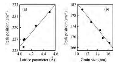
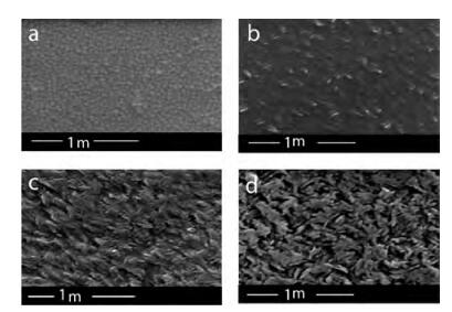
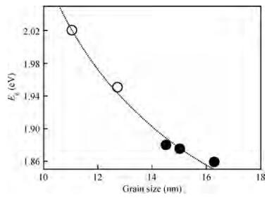
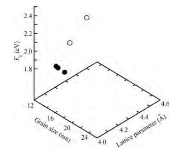
Tin sulphide (SnS) thin films have been recognized as a potential candidate for solar cells. Many fabrication techniques have been used to grow SnS thin films. The band-gap, Eg of SnS films as reported in literature, were found to vary from 1.2-2.5 eV depending on the film fabrication technique. The present work reports the structural, compositional, morphological and optical characterization of SnS thin films fabricated by thermal evaporation at room temperature. Results show that for the given fabrication technique/condition, the band-gap functionally depends on the lattice parameter and grain size. The well-defined variation allows for tailoring SnS film as per requirements.

J. Semicond.
2013, 34(9): 093005 doi: 10.1088/1674-4926/34/9/093005
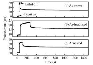
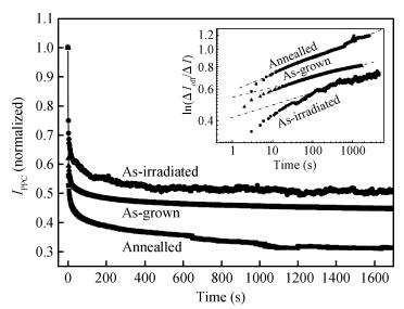
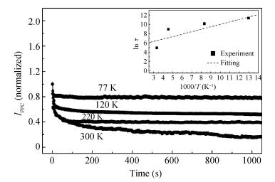
Unintentionally doped GaN films grown by MOCVD were irradiated with neutrons at room temperature. In order to investigate the influence of neutron irradiation on the optical properties of GaN films, persistent photoconductivity (PPC) and low temperature photoluminescence (PL) measurements were carried out. Pronounced PPC was observed in the samples before and after neutron irradiation without the appearance of a yellow luminescence (YL) band in the PL spectrum, suggesting that the origin of PPC and YL are not related. Moreover, PPC phenomenon was enhanced by neutron irradiation and quenched by the followed annealing process at 900℃. The possible origin of PPC is discussed.


J. Semicond.
2013, 34(9): 094001 doi: 10.1088/1674-4926/34/9/094001

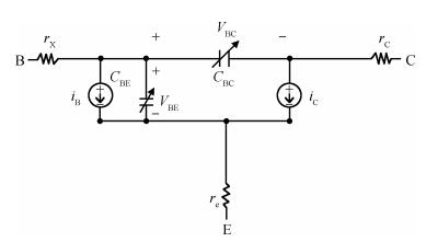
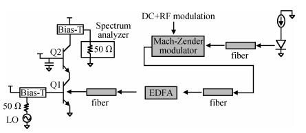
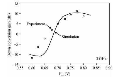
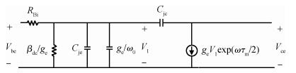
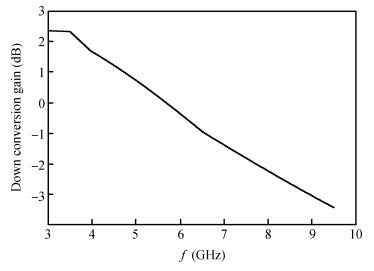
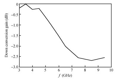
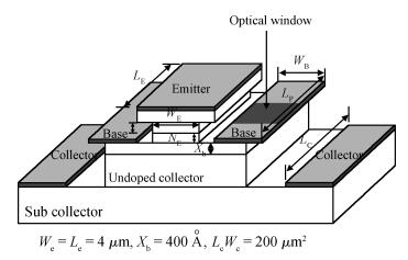
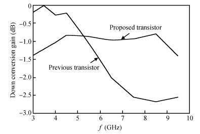
We analyze an integrated electrically pumped opto-electronic mixer, which consists of two InP/GaInAs hetero junction bipolar transistors (HBT), in a cascode configuration. A new HBT with modified physical structure is proposed and simulated to improve the frequency characteristics of a cascode mixer. For the verification and calibrating software simulator, we compare the simulation results of a typical HBT, before modifying it and comparing it with empirical reported experiments. Then we examine the simulator on our modified proposed HBT to prove its wider frequency characteristics with better flatness and acceptable down conversion gain. Although the idea is examined in several GHz modulation, it may easily be extended to state of the art HBT cascode mixers in much higher frequency range.


J. Semicond.
2013, 34(9): 094002 doi: 10.1088/1674-4926/34/9/094002

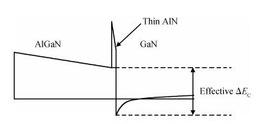
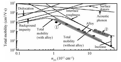
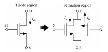
A new surface-potential-based model for AlGaN/AlN/GaN high electron mobility transistor (HEMT) is proposed in this paper. Since the high polarization effects caused by AlN interlayer favorably influence the two dimensional electron gas (2DEG) and scattering mechanisms, we first add spontaneous and piezoelectric charge terms to the source equation of surface-potential, and a mobility model for AlGaN/AlN/GaN HEMT is rewritten. Compared with TCAD simulations, the DC characteristics of AlGaN/AlN/GaN HEMT are faithfully reproduced by the new model.


J. Semicond.
2013, 34(9): 094003 doi: 10.1088/1674-4926/34/9/094003
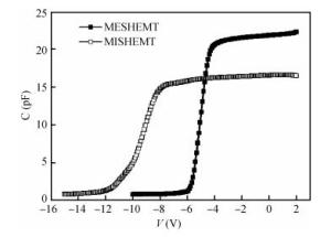
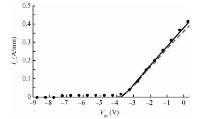
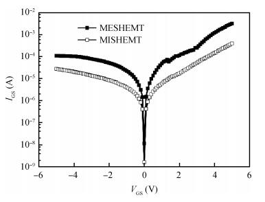
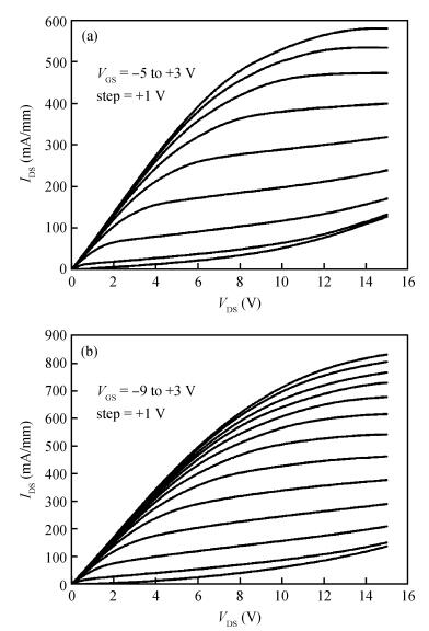
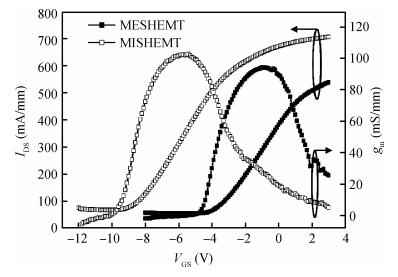
An AlGaN/GaN metal-insulator-semiconductor high-electron-mobility transistor (MISHEMT), with sodium beta-alumina (SBA) for both gate insulation and surface passivation, was investigated and compared with a conventional metal-semiconductor high-electron-mobility transistor (MESHEMT). The measured gate leakage current of the MISHEMT was reduced by approximately one order of magnitude as compared with that of the conventional MESHEMT. The saturation drain current of the AlGaN/GaN MISHEMT reached 830 mA/mm, which was about 43% higher than that of a conventional MESHEMT. The peak extrinsic transconductance of the MISHEMT was 103 mS/mm, which was similarly higher than that of the MESHEMT. The results suggested that the SBA thin film is an effective candidate gate dielectric for AlGaN/GaN MISHEMTs.

J. Semicond.
2013, 34(9): 094004 doi: 10.1088/1674-4926/34/9/094004

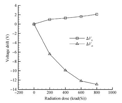
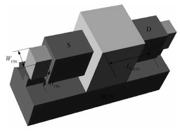
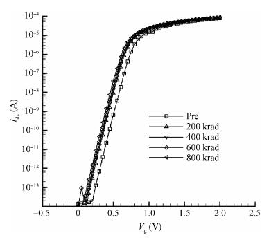
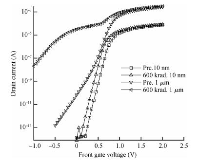
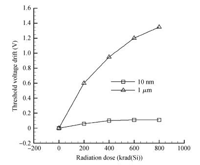
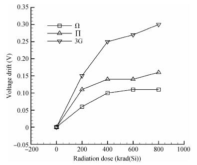
This paper investigates the total ionizing dose response of different non-planar triple-gate transistor structures with different fin widths. By exposing the pseudo-MOS transistor to different amounts of radiation, different interface trap densities and trapped-oxide charges can be obtained. Using these parameters together with Altal 3D simulation software, the total dose radiation response of various non-planar triple-gate devices can be simulated. The behaviors of three kinds of non-planar devices are compared.


J. Semicond.
2013, 34(9): 094005 doi: 10.1088/1674-4926/34/9/094005

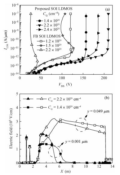
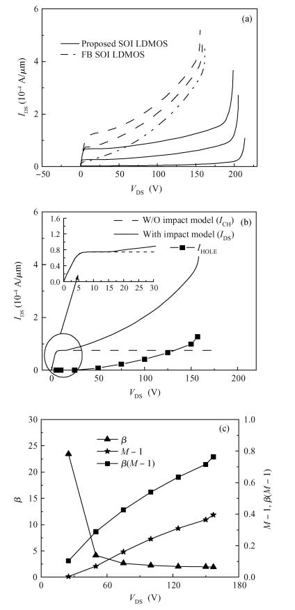
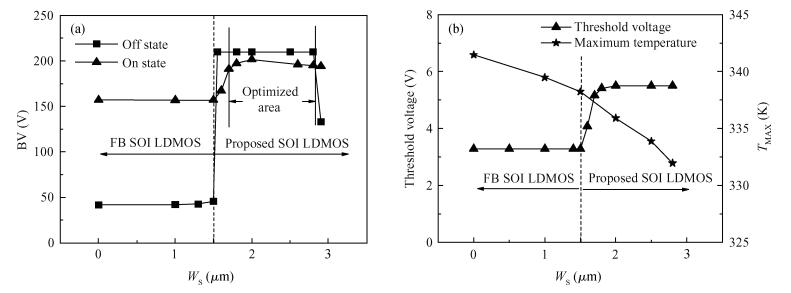
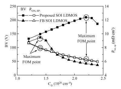
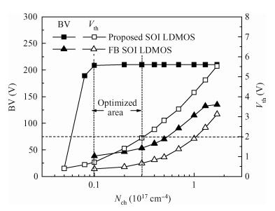
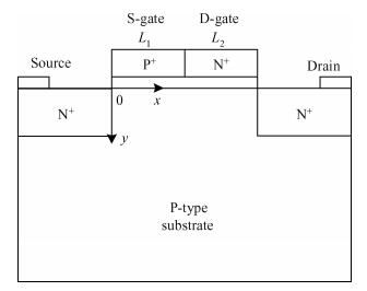
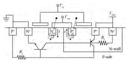
A novel CMOS-compatible thin film SOI LDMOS with a novel body contact structure is proposed. It has a Si window and a P-body extended to the substrate through the Si window, thus, the P-body touches the P+ region to form the body contact. Compared with the conventional floating body SOI LDMOS (FB SOI LDMOS) structure, the new structure increases the off-state BV by 54%, decreases the specific on resistance by 20%, improves the output characteristics significantly, and suppresses the self-heating effect. Furthermore, the advantages of the low leakage current and low output capacitance of SOI devices do not degrade.


J. Semicond.
2013, 34(9): 094006 doi: 10.1088/1674-4926/34/9/094006

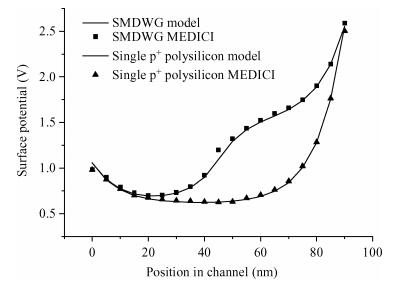
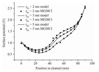
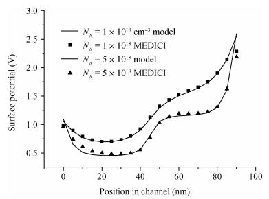
An analytical surface potential model for the single material double work function gate (SMDWG) MOSFET is developed based on the exact resultant solution of the two-dimensional Poisson equation. The model includes the effects of drain biases, gate oxide thickness, different combinations of S-gate and D-gate length and values of substrate doping concentration. More attention has been paid to seeking to explain the attributes of the SMDWG MOSFET, such as suppressing drain-induced barrier lowering (DIBL), accelerating carrier drift velocity and device speed. The model is verified by comparison to the simulated results using the device simulator MEDICI. The accuracy of the results obtained using our analytical model is verified using numerical simulations. The model not only offers the physical insight into device physics but also provides the basic designing guideline for the device.


J. Semicond.
2013, 34(9): 094007 doi: 10.1088/1674-4926/34/9/094007

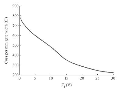
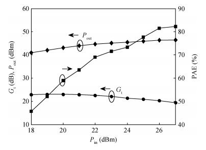
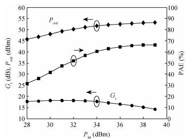
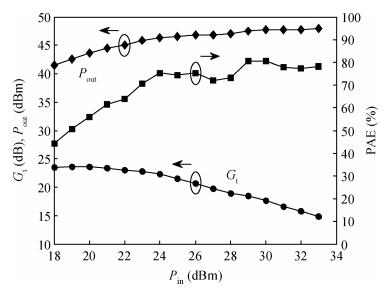
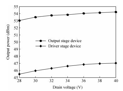
Two types of RF LDMOS devices, specified for application in the driver stage and output stage of a power amplifier, are designed based on a modified CMOS process. By optimizing the layout and process, the output capacitance per unit of gate width is as low as 225 fF/mm. The driver stage and output stage devices achieve an output power of 44 W with a PAE of 82% and 230 W with a PAE of 72.3%, respectively (P3dB compression) at 1 GHz. Both devices are capable of withstanding extremely severe ruggedness tests without any performance degradation. These tests are 3-5 dB overdrive, 10:1 voltage standing wave ratio mismatch load through all phase angles, and 40% drain overvoltage elevation at a working point of P3dB.


J. Semicond.
2013, 34(9): 094008 doi: 10.1088/1674-4926/34/9/094008

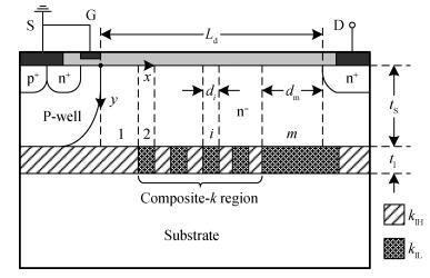
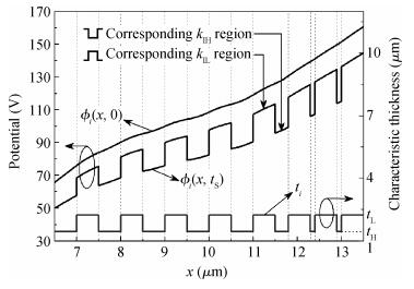
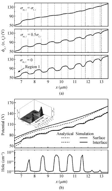
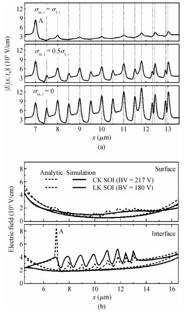
An analytical model for a novel high voltage silicon-on-insulator device with composite-k (relative permittivity) dielectric buried layer (CK SOI) is proposed. In this structure, the composite-k buried layer is composed by alternating Si3N4 and low-k (k=2.65) dielectric in the lateral direction. Due to the composite-k buried layer, the breakdown voltage (BV) is improved both by the vertical and lateral direction. Taking the modulation effect of accumulated interface holes into account, an analytical model is developed. In the blocking state, the proposed model revealed the mechanism of hole accumulation above the Si3N4 buried layer and investigated the modulation effect of accumulated holes on the two-dimensional (2-D) potential and electric field distributions. This analytical model is verified by the simulation results. Compared with the low-k dielectric buried layer SOI (LK SOI), simulation results show that the BV for CK SOI is enhanced by 21% and the specific on-resistance is reduced by 32%, respectively.


J. Semicond.
2013, 34(9): 094009 doi: 10.1088/1674-4926/34/9/094009

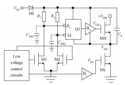
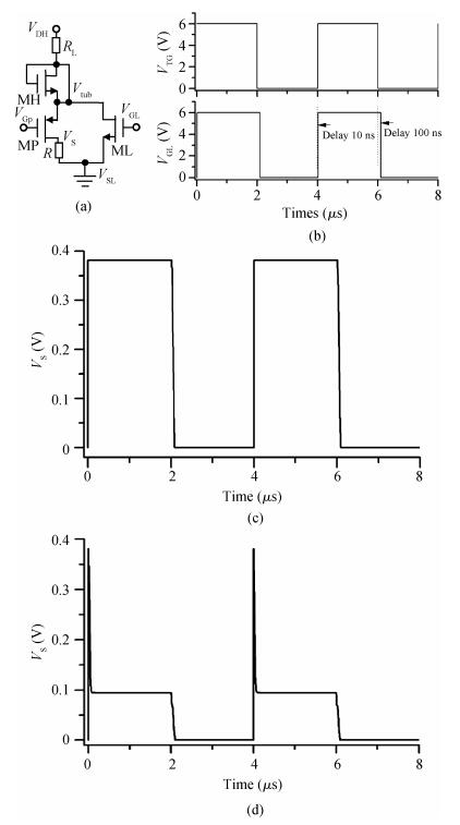
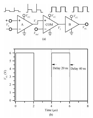
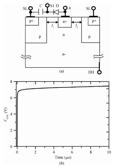
Novel high-voltage, high-side and low-side power devices, whose control circuits are referred to as the tub, are proposed and investigated to reduce chip area and improve the reliability of high-voltage integrated circuits. By using the tub circuit to control a branch circuit consisting of a PMOS and a resistor, a pulse signal is generated to control the low-side n-LDMOS after being processed by a low-voltage circuit. Thus, the high-voltage level-shifting circuit is not needed any more, and the parasitic effect of the conventional level-shifting circuit is eliminated. Moreover, the specific on-resistance of the proposed low-side device is reduced by more than 14.3% compared with the conventional one. In the meantime, integrated low-voltage power supplies for the low-voltage circuit and the tub circuit are also proposed. Simulations are performed with MEDICI and SPICE, and the results show that the expectant functions are achieved well.


J. Semicond.
2013, 34(9): 094010 doi: 10.1088/1674-4926/34/9/094010
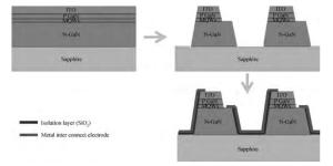
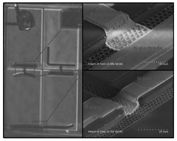
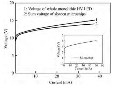
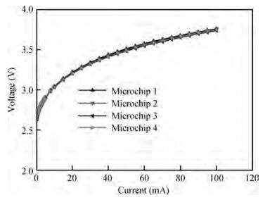
We report a new monolithic structure of GaN-based light-emitting diode (LED) which can be operated under high voltage or alternative current. Differing from the conventional single LED chip, the monolithic light-emitting diode (MLED) array contains microchips which are interconnected in series or parallel. The key chip fabrication processing methods of the monolithic LED array include deep dry etching, sidewall insulated protection, and electrode interconnection. A 12 V GaN-based blue high voltage light emitting diode was designed and fabricated in our experiment. The forward current-voltage characteristics of MLEDs were consistent with those of conventional single junction light emitting diodes.


J. Semicond.
2013, 34(9): 094011 doi: 10.1088/1674-4926/34/9/094011

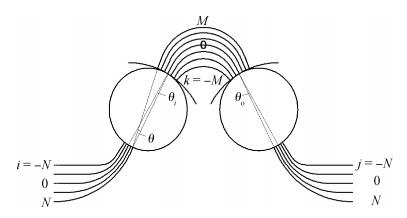
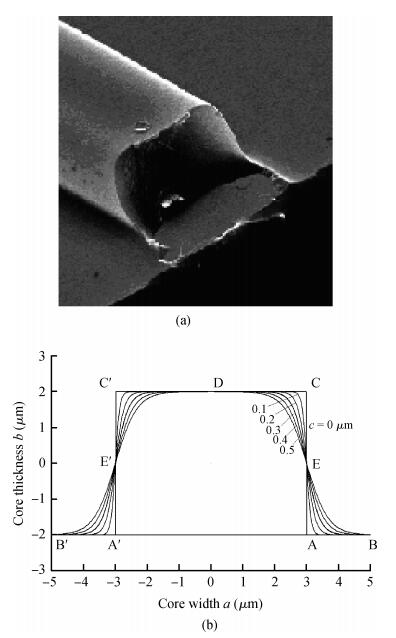
Based on transmission theory, a 17×17 polymer arrayed waveguide grating (AWG) multiplexer parameter optimization is performed, and the influence of the fabrication results on the transmission characteristics are analyzed. In this paper, we mainly discuss three of the main errors in the fabrication of polymer AWG devices. One is δ n1, which is caused by the tuning of the core refractive index n1, the second is δ b, which results from the rotating-coating of the core thickness b, and the other is the non-ideal core cross-section, which is caused by steam redissolution. The effects of the above fabrication errors on the transmission characteristics of the AWG device are investigated, and compensation techniques are proposed. By comparing the theoretical simulation and experimental results, the shift in the transmission spectrum is reduced by 0.028 nm, the 3 dB bandwidth is increased by about 0.036 nm, the insertion loss is reduced by about 3 dB for the central channel and 4.5 dB for the edge channels, and the crosstalk is reduced by 1.5 dB.


J. Semicond.
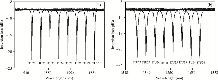
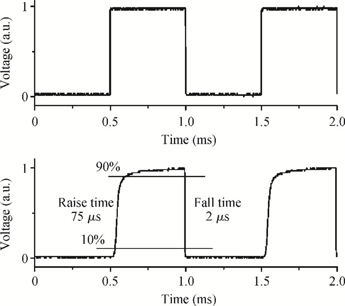
2013, 34(9): 094012 doi: 10.1088/1674-4926/34/9/094012
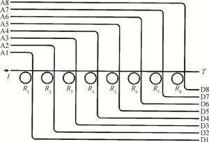
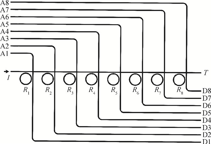
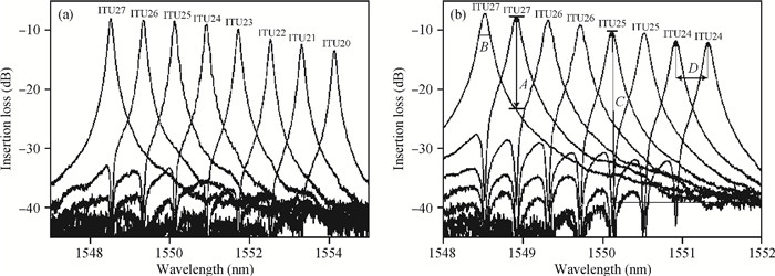
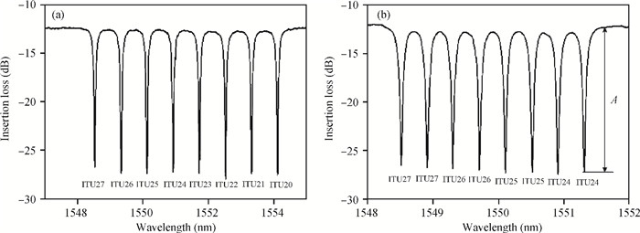
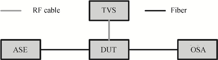
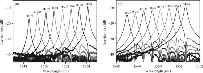
We report on an eight-channel reconfigurable optical add-drop multiplexer based on cascaded microring resonators with a high tuning power consumption and a compact footprint. Microheaters are fabricated on top of the microring resonators and can be modulated using the thermo-optic effect to achieve the reconfigurable functionality of the device. We demonstrate the reconfigurable add-drop multiplexing functionality for channel spacings of 100 GHz and 50 GHz, with the centre wavelengths of the channels aligned to International Telecommunication Union grid specifications. The crosstalk for channel spacings of 100 GHz and 50 GHz are less than -22.5 dB and -15.5 dB, respectively. The average tuning efficiency is about 4.5 mW/nm, and the response speed is about 13.0 kHz.


J. Semicond.
2013, 34(9): 095001 doi: 10.1088/1674-4926/34/9/095001

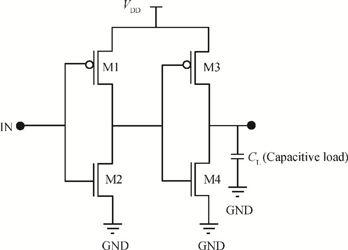
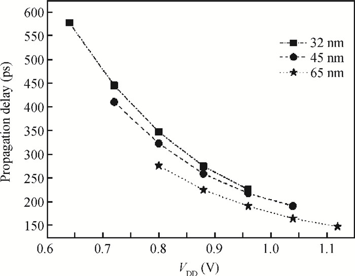
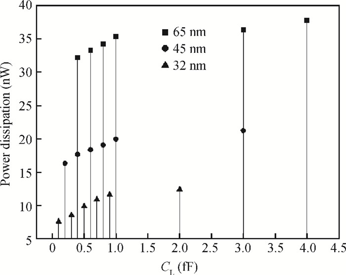
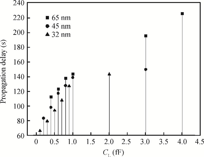
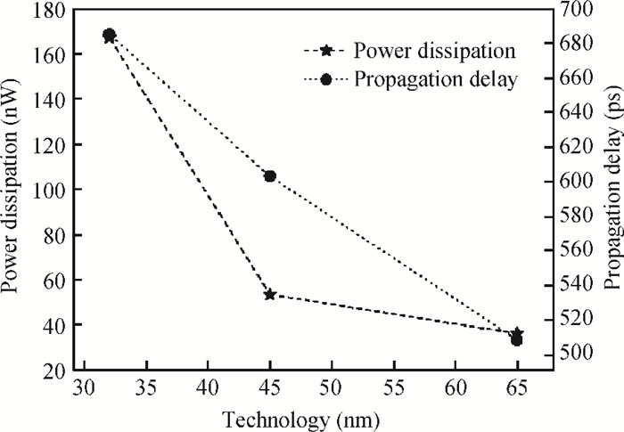
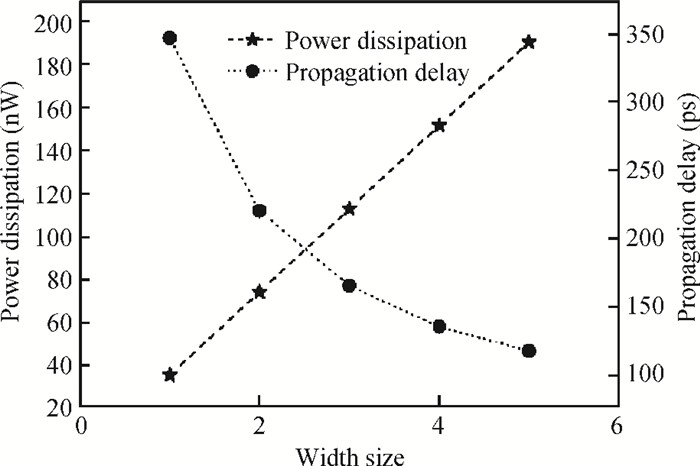
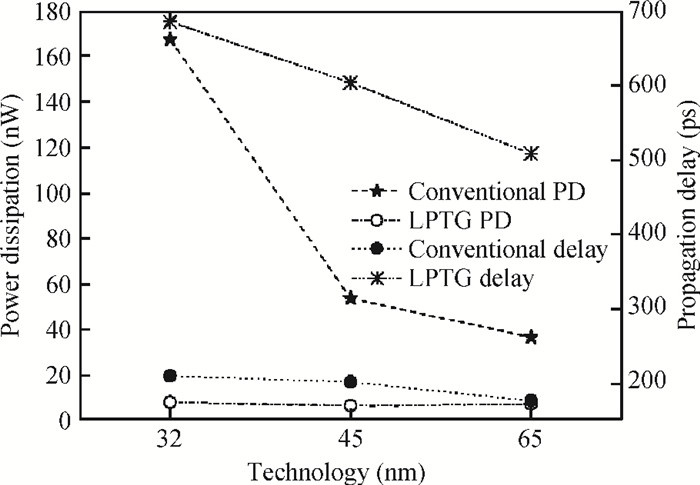
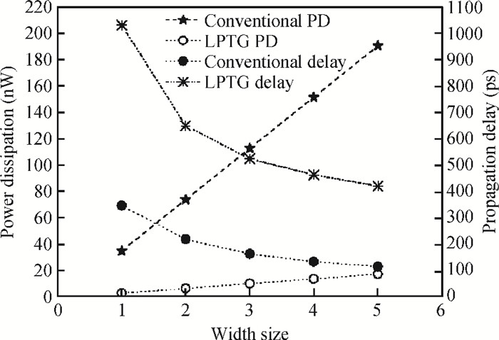
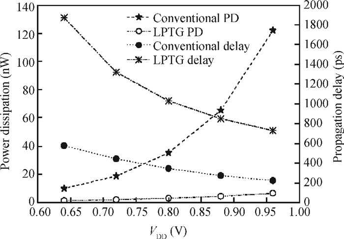
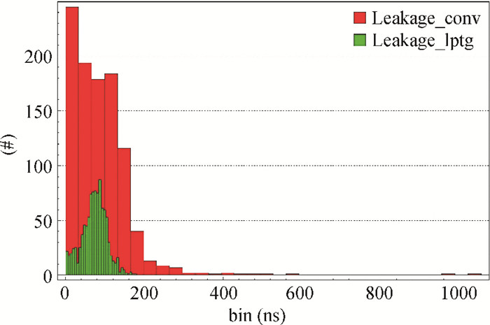
Device scaling is an important part of the very large scale integration (VLSI) design to boost up the success path of VLSI industry, which results in denser and faster integration of the devices. As technology node moves towards the very deep submicron region, leakage current and circuit reliability become the key issues. Both are increasing with the new technology generation and affecting the performance of the overall logic circuit. The VLSI designers must keep the balance in power dissipation and the circuit's performance with scaling of the devices. In this paper, different scaling methods are studied first. These scaling methods are used to identify the effects of those scaling methods on the power dissipation and propagation delay of the CMOS buffer circuit. For mitigating the power dissipation in scaled devices, we have proposed a reliable leakage reduction low power transmission gate (LPTG) approach and tested it on complementary metal oxide semiconductor (CMOS) buffer circuit. All simulation results are taken on HSPICE tool with Berkeley predictive technology model (BPTM) BSIM4 bulk CMOS files. The LPTG CMOS buffer reduces 95.16% power dissipation with 84.20% improvement in figure of merit at 32 nm technology node. Various process, voltage and temperature variations are analyzed for proving the robustness of the proposed approach. Leakage current uncertainty decreases from 0.91 to 0.43 in the CMOS buffer circuit that causes large circuit reliability.


J. Semicond.
2013, 34(9): 095002 doi: 10.1088/1674-4926/34/9/095002

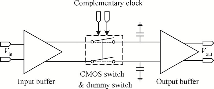
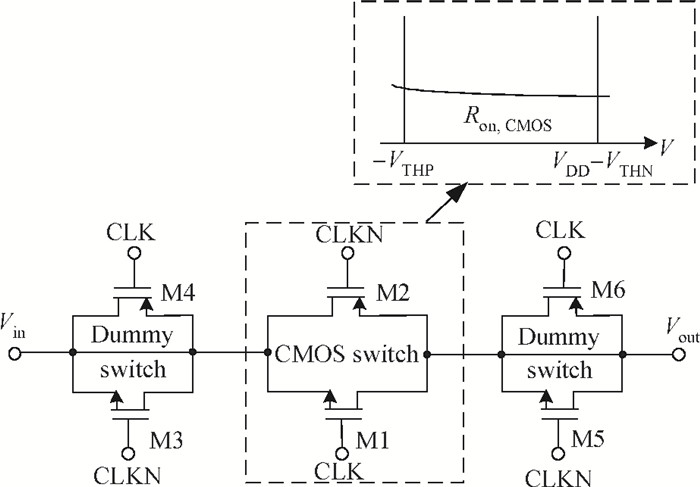
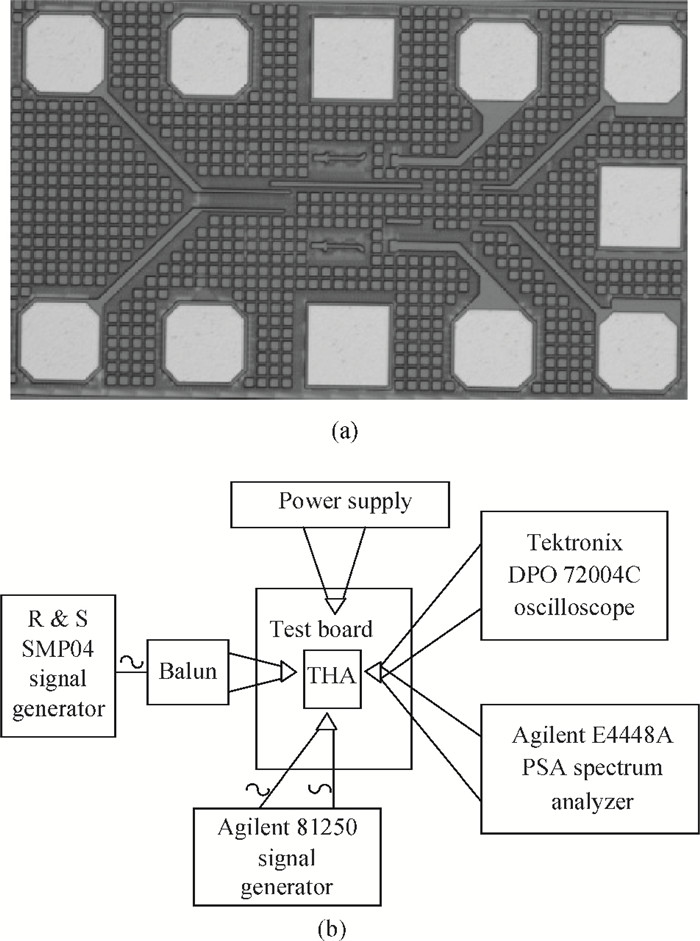
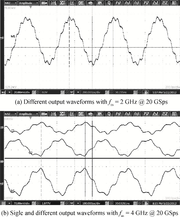
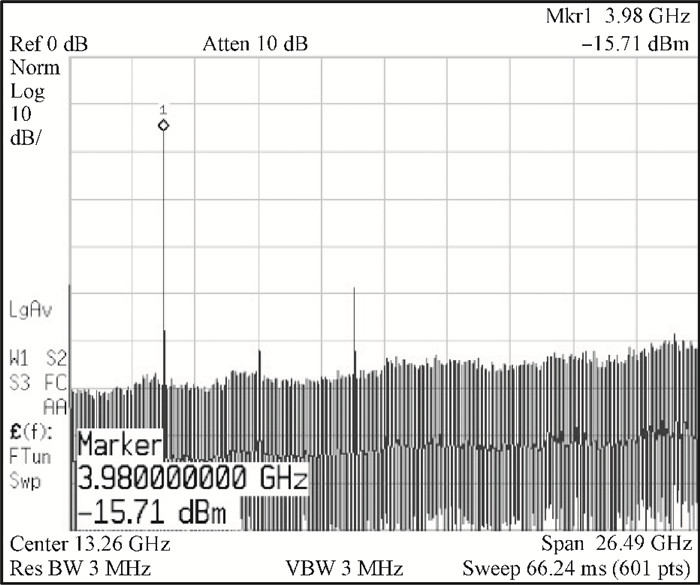
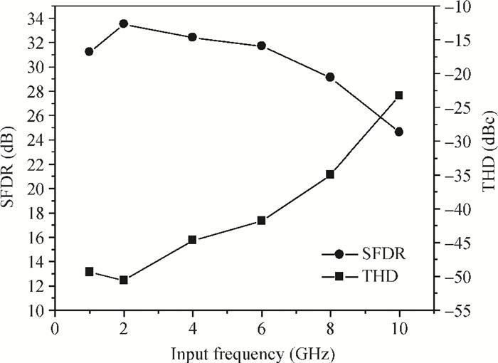
An open-loop 20 GSps track-and-hold amplifier (THA) using fully-differential architecture to mitigate common-mode noise and suppress even-order harmonics is presented. CMOS switch and dummy switches are adopted to achieve high speed and good linearity. A cross-coupled pair is used in the input buffer to suppress the charge injection and clock feedthrough. Both the input and output buffers use an active inductor load to achieve high signal bandwidth. The THA is realized with 0.18 μm SiGe BiCMOS technology using only CMOS devices at a 1.8 V voltage supply and with a core area of 0.024 mm2. The measurement results show that the SFDR is 32.4 dB with a 4 GHz sine wave input at a 20 GSps sampling rate, and the third harmonic distortion is -48 dBc. The effective resolution bandwidth of the THA is 12 GHz and the figure of merit is only 0.028 mW/GHz.


J. Semicond.
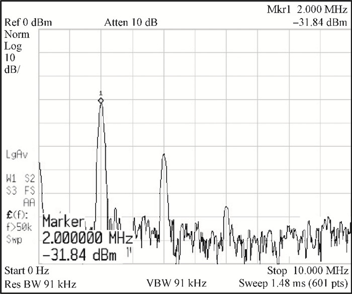
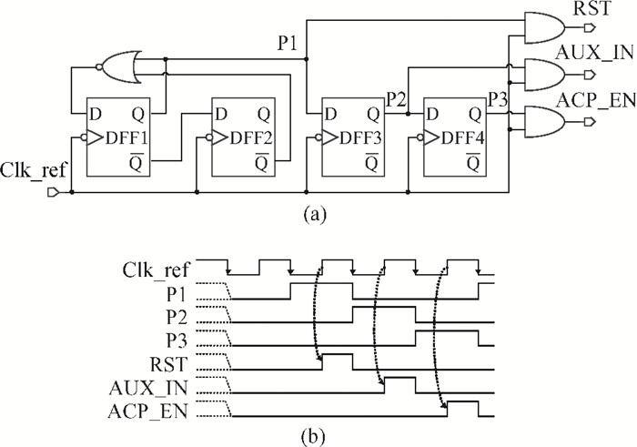
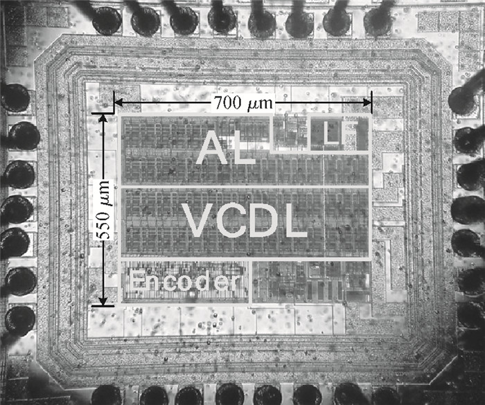
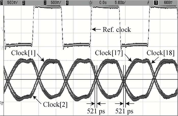
2013, 34(9): 095003 doi: 10.1088/1674-4926/34/9/095003

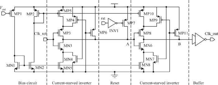
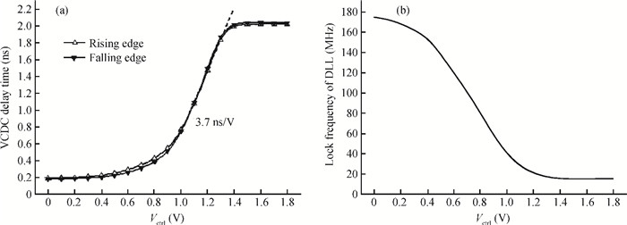
A time-to-digital converter (TDC) based on a reset-free and anti-harmonic delay-locked loop (DLL) circuit for wireless positioning systems is discussed and described. The DLL that generates 32-phase clocks and a cycle period detector is employed to avoid "false locking". Driven by multiphase clocks, an encoder detects pulses and outputs the phase of the clock when the pulse arrives. The proposed TDC was implemented in SMIC 0.18 μm CMOS technology, and its core area occupies 0.7×0.55 mm2. The reference frequency ranges from 20 to 150 MHz. An LSB resolution of 521 ps can be achieved by using a reference clock of 60 MHz and the DNL is less than ±0.75 LSB. It dissipates 31.5 mW at 1.8 V supply voltage.


J. Semicond.
2013, 34(9): 095004 doi: 10.1088/1674-4926/34/9/095004

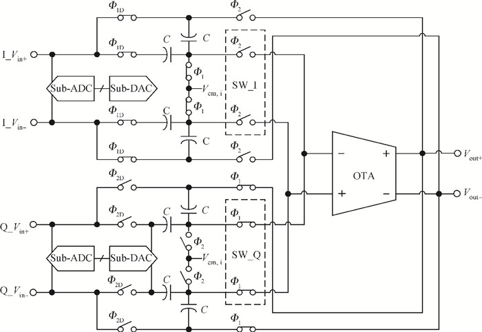
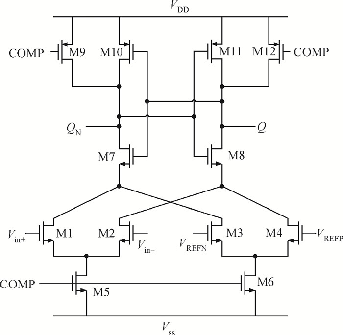
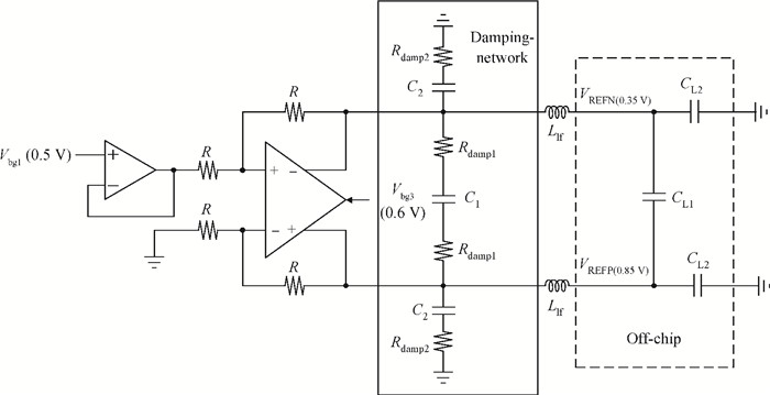
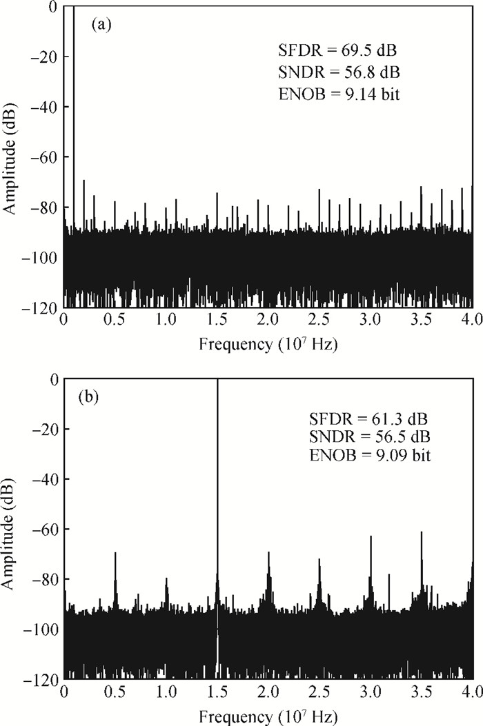
A power-efficient technique for pipeline analog-to-digital converters (ADCs) is proposed. By sharing amplifiers between I/Q channels, the power dissipation of the ADCs is reduced by almost one-half compared to conventional topologies, which makes this technique suitable for low-power direct-conversion WLAN receivers. A dual-channel ADC test chip is fabricated in 55 nm CMOS technology. The 10 bit ADC with on-chip reference generators dissipates 19.2 mW per channel from a 1.2 V supply. At an 80 MS/s sample rate, the measured spurious-free dynamic range, signal-to-noise and distortion ratio, and corresponding effective number of bits are 69.5 dB, 56.8 dB and 9.14 bits with a 1 MHz input frequency (fin), and 61.3 dB, 56.5 dB and 9.09 bits with a 15 MHz fin, respectively. The active area is 1.01×0.77 mm2.


J. Semicond.
2013, 34(9): 095005 doi: 10.1088/1674-4926/34/9/095005

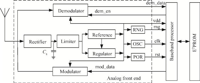
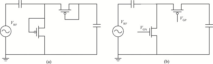
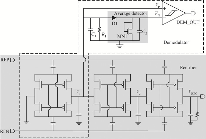
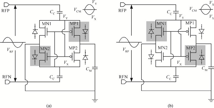
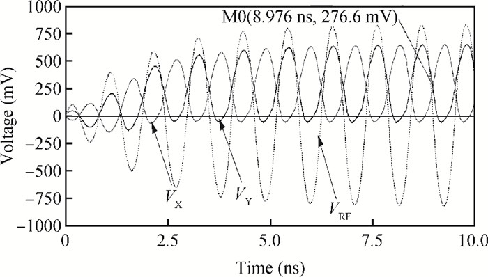
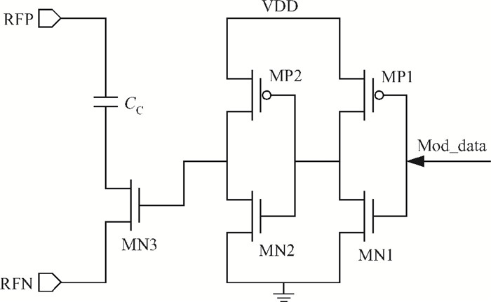
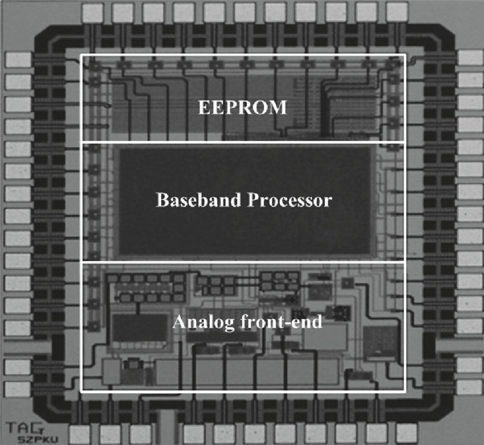
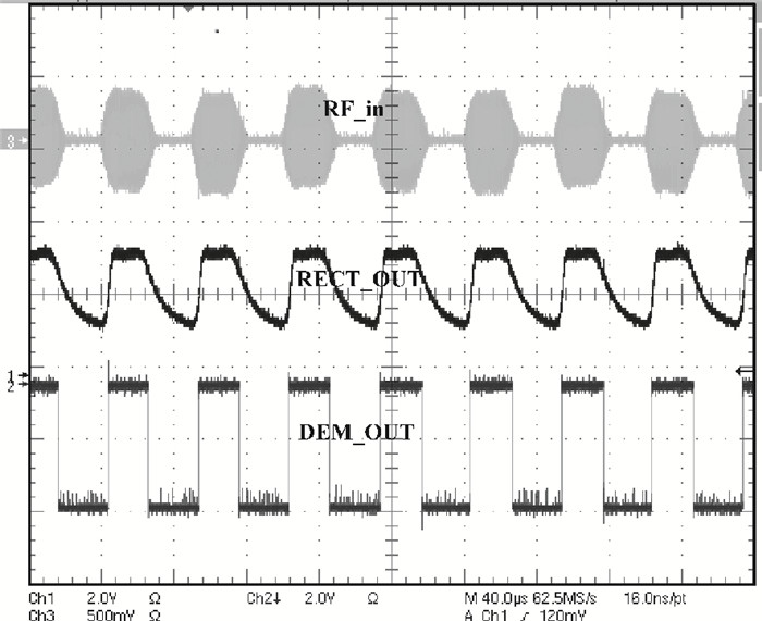
This paper presents a passive UHF RFID tag with a dynamic-Vth-cancellation (DVC) rectifier. In the rectifier, the threshold voltages of MOSFETs are cancelled by applying gate bias voltages, which are dynamically changed according to the states of the MOSFETs. The DVC rectifier enables both low ON-resistance and small reverse leakage of the MOSFETs, resulting in high power conversion efficiency (PCE). An area-efficient demodulator with a novel average detector is also designed, which takes advantage of the rectifier's first stage as the envelope detector. The whole tag chip is implemented in a 0.18 μm CMOS process with a die size of 880×950 μm2. Measurement results show that the rectifier achieves a maximum PCE of 53.7% with 80 kΩ resistor load.

J. Semicond.
2013, 34(9): 095006 doi: 10.1088/1674-4926/34/9/095006
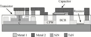
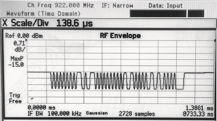
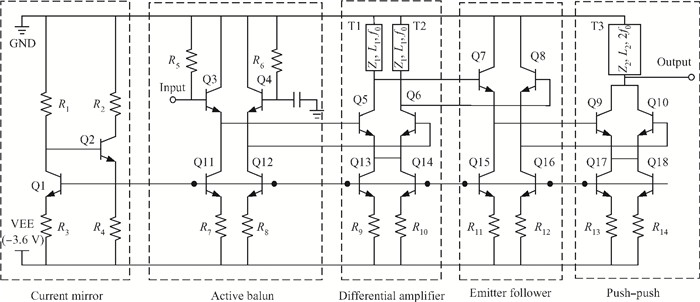
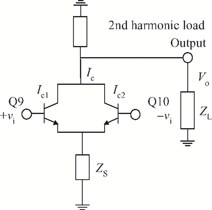
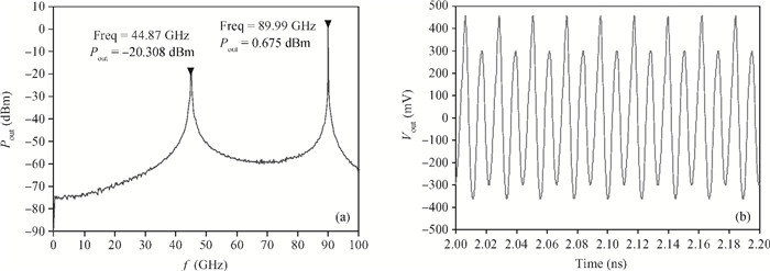
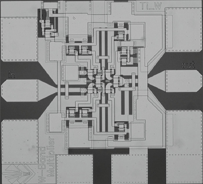
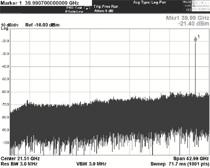
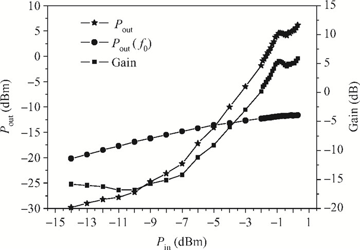
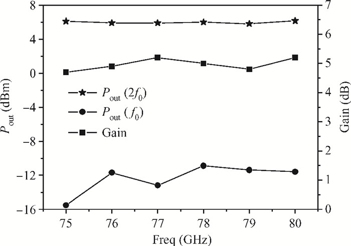
A W-band frequency doubler MMIC is designed and fabricated using 1-μm InP DHBT technology. Active balun is employed to transform the single-ended signal into differential output. Push-push configuration loaded with harmonic resonant network is utilized to acquire the second harmonic frequency. A multi-stage differential structure improves the conversion gain and suppresses the fundamental frequency. The MMIC occupies an area of 0.55×0.5 mm2 with 18 DHBTs integrated. Measurements show that the output power is above 5.8 dBm with the suppression of fundamental frequency below -16 dBc and the conversion gain above 4.7 dB over 75-80 GHz.


J. Semicond.
2013, 34(9): 095007 doi: 10.1088/1674-4926/34/9/095007

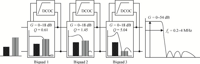
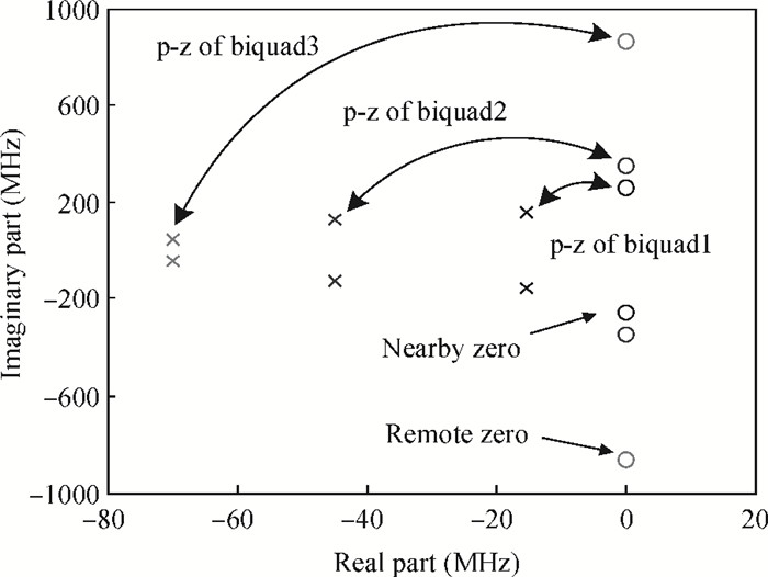
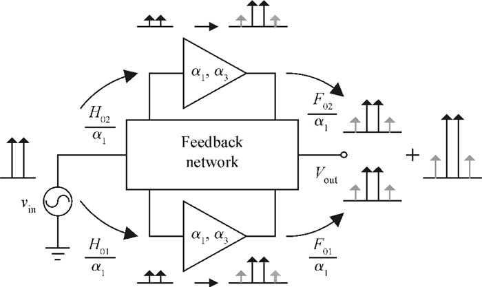
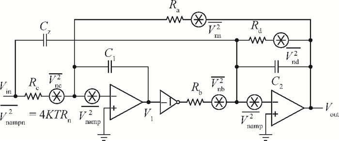
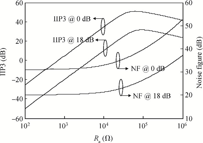
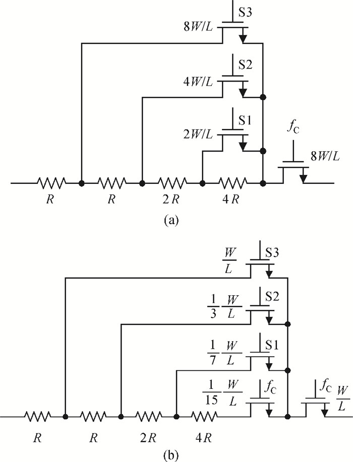
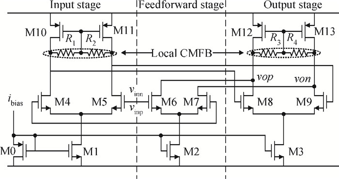
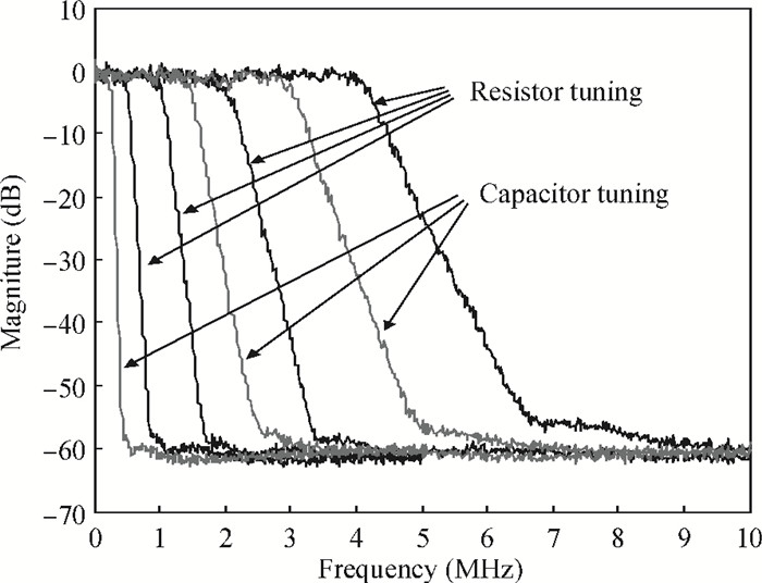
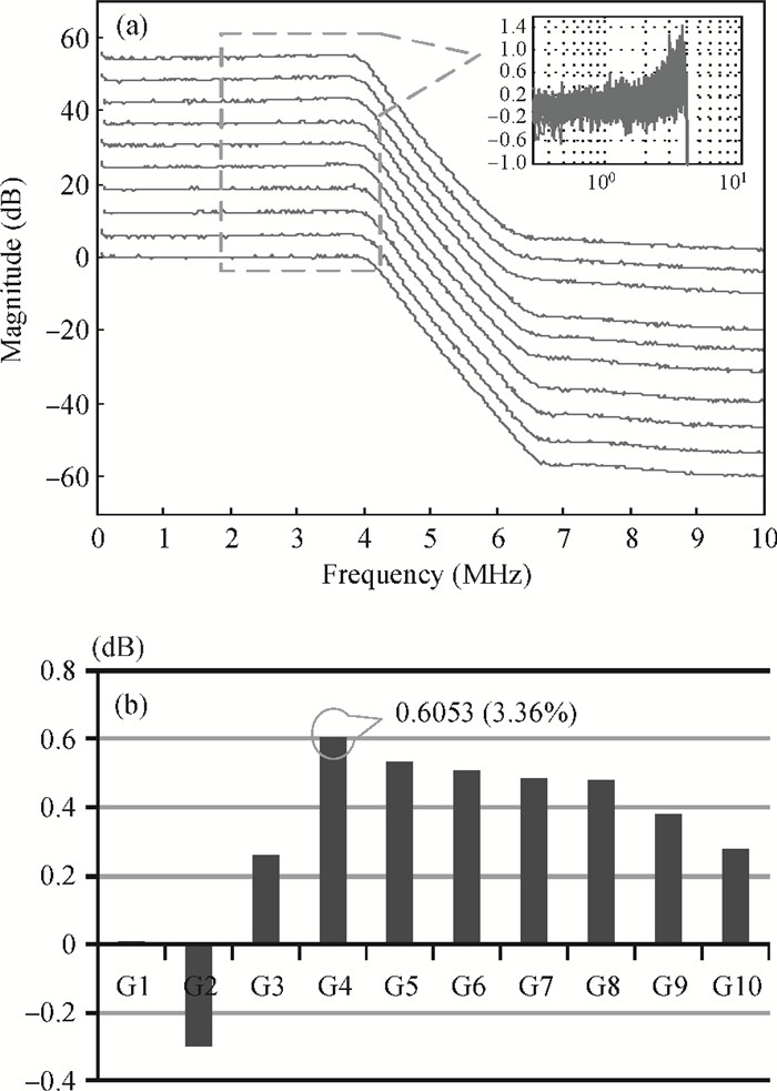
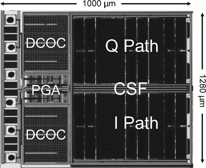
This paper presents a channel-select filter that employs an active-RC bi-quad structure for TV-tuner application. A design method to optimize the ⅡP3 of the bi-quad is developed. Multi-band selection and gain adjustment are implemented using switching resistors in the resistor array and capacitors in the capacitor array. Q-factor degradation is compensated by a tuning segmented resistor. A feed-forward OTA with high gain and low third-order distortion is applied in the bi-quad to maximize linearity performance and minimize area by avoiding extra compensation capacitor use. An RC tuning circuit and DC offset cancellation circuit are designed to overcome the process variation and DC offset, respectively. The experimental results yield an in-band ⅡP3 of more than 31 dBm at 0 dB gain, a 54 dB gain range with 6 dB gain step, and a continuous frequency tuning range from 0.25 to 4 MHz. The in-band ripple is less than 1.4 dB at high gain mode, while the gain error and frequency tuning error are no more than 3.4% and 5%, respectively. The design, which is fabricated in a 0.18 μm CMOS process, consumes 12.6 mW power at a 1.8 V supply and occupies 1.28 mm2.


J. Semicond.
2013, 34(9): 095008 doi: 10.1088/1674-4926/34/9/095008

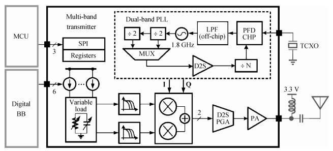
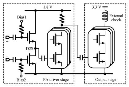
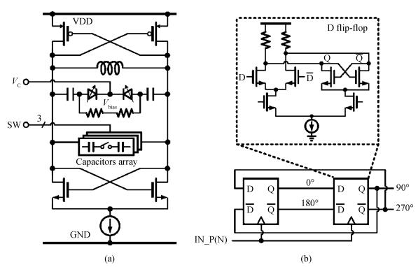
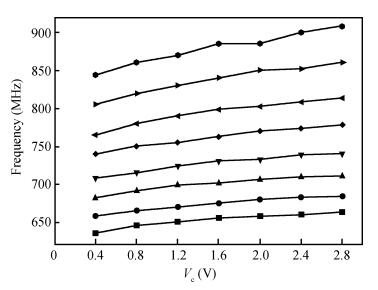
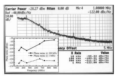
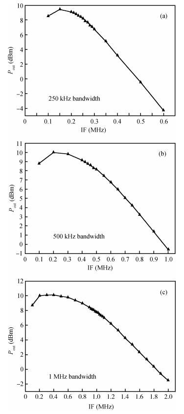
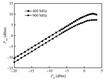
A reconfigurable multi-mode direct-conversion transmitter (TX) with integrated frequency synthesizer (FS) is presented. The TX as well as the FS is designed with a flexible architecture and frequency plan, which helps to support all the 433/868/915 MHz ISM band signals, with the reconfigurable bandwidth from 250 kHz to 2 MHz. In order to save power and chip area, only one 1.8 GHz VCO is adopted to cover the whole frequency range. All the operation modes can be regulated in real time by configuring the integrated register-bank through an SPI interface. Implemented in 180 nm CMOS, the FS achieves a frequency coverage of 320-460 MHz and 620-920 MHz. The lowest phase noise can be -107 dBc/Hz at a 100 kHz offset and -126 dBc/Hz at a 1 MHz offset. The transmitter features a +10.2 dBm peak output power with a +9.5 dBm 1-dB-compression point and 250 kHz/500 kHz/1 MHz/2 MHz reconfigurable signal bandwidth.


J. Semicond.
2013, 34(9): 095009 doi: 10.1088/1674-4926/34/9/095009

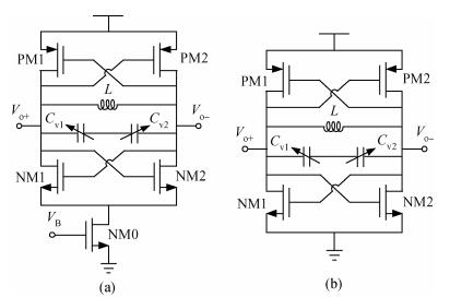
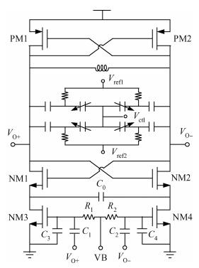
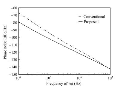
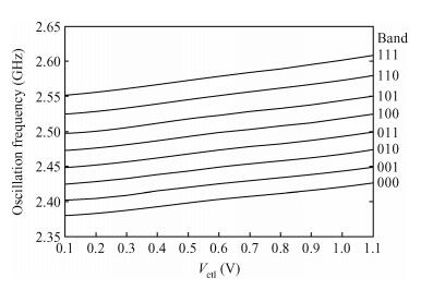
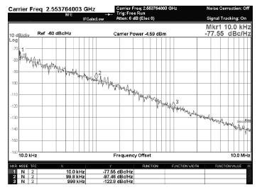
To meet the requirements of the low power Zigbee system, VCO design optimizations of phase noise, power consumption and frequency tuning are discussed in this paper. Both flicker noise of tail bias transistors and up-conversion of flicker noise from cross-coupled pair are reduced by improved self-switched biasing technology, leading to low close-in phase noise. Low power is achieved by low supply voltage and triode region biasing. To linearly tune the frequency and get constant gain, distributed varactor structure is adopted. The proposed VCO is fabricated in SMIC 0.18-μm CMOS process. The measured linear tuning range is from 2.38 to 2.61 GHz. The oscillator exhibits low phase noise of -77.5 dBc/Hz and -122.8 dBc/Hz at 10 kHz and 1 MHz offset, respectively, at 2.55 GHz oscillation frequency while dissipating 2.7 mA from 1.2 V supply voltage, which well meet design specifications.


J. Semicond.
2013, 34(9): 095010 doi: 10.1088/1674-4926/34/9/095010
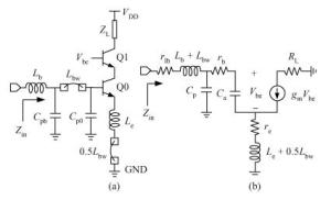
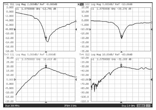
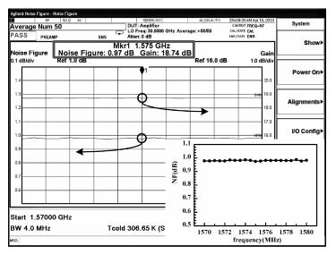
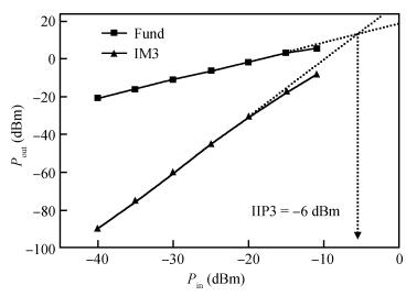
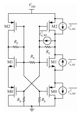
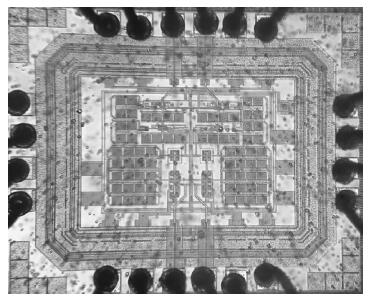
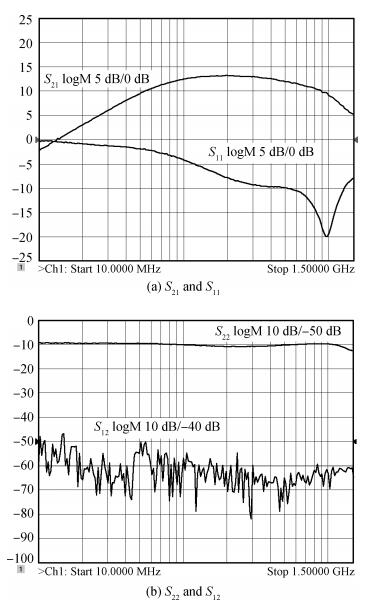
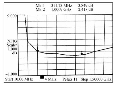
A monolithic integrated low noise amplifier (LNA) based on a SiGe HBT process for a global navigation satellite system (GNSS) is presented. An optimizing strategy of taking parasitic capacities at the input node into consideration is adopted and a method and design equations of monolithically designing the LC load and the output impedance matching circuit are introduced. The LNA simultaneously reaches excellent noise and input/output impedance matching. The measurement results show that the LNA gives an ultra-low noise figure of 0.97 dB, a power gain of 18.6 dB and a three-order input intermodulation point of -6 dBm at the frequency of 1.575 GHz. The chip consumes 5.4 mW from a 1.8 V source and occupies 600×650 μm2 die area.


J. Semicond.
2013, 34(9): 095011 doi: 10.1088/1674-4926/34/9/095011

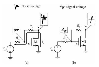
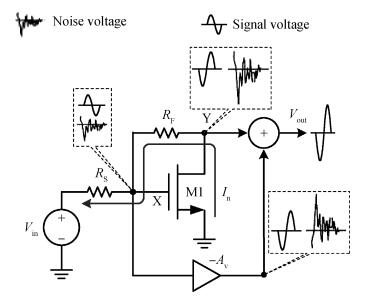
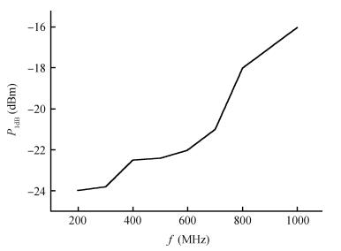
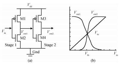
A wideband inductorless low noise amplifier for digital TV tuner applications is presented. The proposed LNA scheme uses a composite NMOS/PMOS cross-coupled transistor pair to provide partial cancellation of noise generated by the input transistors. The chip is implemented in SMIC 0.18 μm CMOS technology. Measurement shows that the proposed LNA achieves 12.2-15.2 dB voltage gain from 300 to 900 MHz, the noise figure is below 3.1 dB and has a minimum value of 2.3 dB, and the best input-referred 1-dB compression point (IP1dB) is -17 dBm at 900 MHz. The core consumes 7 mA current with a supply voltage of 1.8 V and occupies an area of 0.5×0.35 mm2.
J. Semicond.
2013, 34(9): 095012 doi: 10.1088/1674-4926/34/9/095012

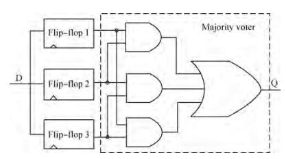
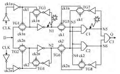
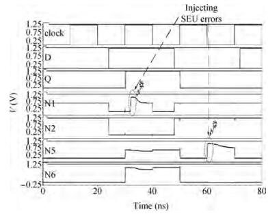
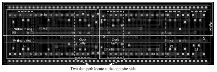
A radiation-hardened flip-flop is proposed to mitigate the single event upset (SEU) effect. Immunity was achieved through the use of C-elements and redundant storage elements. It takes advantage of the property of a C-element in which it enters a high impedance mode when its inputs are of different logic values. Redundant storage nodes are then used to drive the C-elements so that a single upset pulse in any storage will be prevented from altering the state of the output of the flip-flop. The flip-flop was implemented using 48 transistors and occupied an area of 30.78 μm2, using 65 nm CMOS process. It consumed 22.6% fewer transistors as compared to the traditional SEU resilient TMR flip-flop.


J. Semicond.
2013, 34(9): 095013 doi: 10.1088/1674-4926/34/9/095013

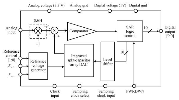
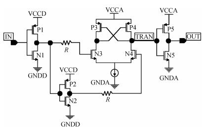
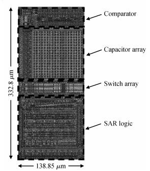
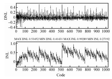
An area-efficient CMOS 1-MS/s 10-bit charge-redistribution SAR ADC for battery voltage measurement in a SoC chip is proposed. A new DAC architecture presents the benefits of a low power approach without applying the common mode voltage. The threshold inverter quantizer (TIQ)-based CMOS Inverter is used as a comparator in the ADC to avoid static power consumption which is attractive in battery-supply application. Sixteen level-up shifters aim at converting the ultra low core voltage control signals to the higher voltage level analog circuit in a 55 nm CMOS process. The whole ADC power consumption is 2.5 mW with a maximum input capacitance of 12 pF in the sampling mode. The active area of the proposed ADC is 0.0462 mm2 and it achieves the SFDR and ENOB of 65.6917 dB and 9.8726 bits respectively with an input frequency of 200 kHz at 1 MS/s sampling rate.


J. Semicond.
2013, 34(9): 095014 doi: 10.1088/1674-4926/34/9/095014

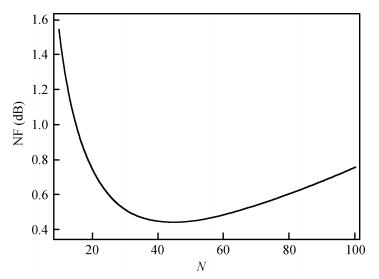
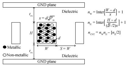
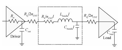
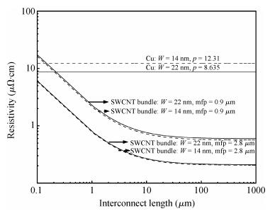
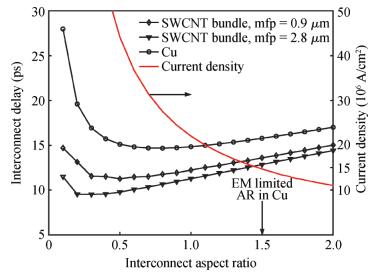
Metallic carbon nanotubes (CNTs) have been proposed as a promising alternative to Cu interconnects in future integrated circuits (ICs) for their remarkable conductive, mechanical and thermal properties. Compact equivalent circuit models for single-walled carbon nanotube (SWCNT) bundles are described, and the performance of SWCNT bundle interconnects is evaluated and compared with traditional Cu interconnects at different interconnect levels for through-silicon-via-based three dimensional (3D) ICs. It is shown that at a local level, CNT interconnects exhibit lower signal delay and smaller optimal wire size. At intermediate and global levels, the delay improvement becomes more significant with technology scaling and increasing wire lengths. For 1 mm intermediate and 10 mm global level interconnects, the delay of SWCNT bundles is only 49.49% and 52.82% that of the Cu wires, respectively.


J. Semicond.
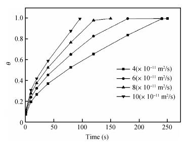
2013, 34(9): 096001 doi: 10.1088/1674-4926/34/9/096001

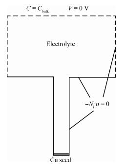
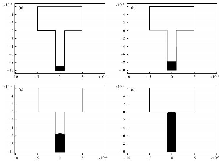
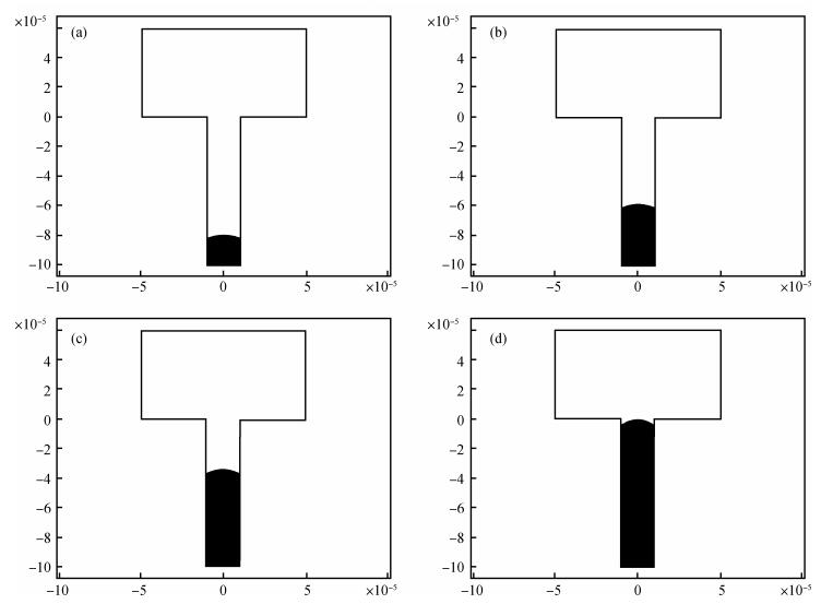
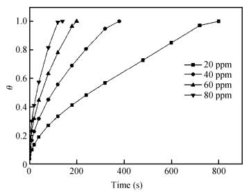
Filling high aspect ratio through silicon vias (TSVs) without voids and seams by copper plating is one of the technical challenges for 3D integration. Bottom-up copper plating is an effective solution for TSV filling. In this paper, a new numerical model was developed to simulate the electrochemical deposition (ECD) process, and the influence of an accelerator in the electrolyte was investigated. The arbitrary Lagrange-Eulerian (ALE) method for solving moving boundaries in the finite element method (FEM) was used to simulate the electrochemical process. In the model, diffusion coefficient and adsorption coefficient were considered, and then the time-resolved evolution of electroplating profiles was simulated with ion concentration distribution and the electric current density.