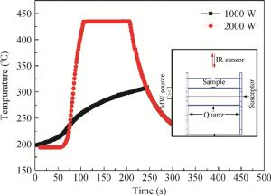
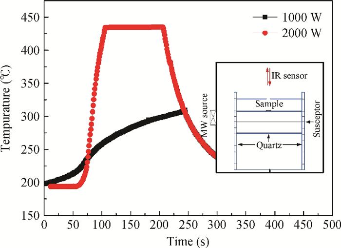
Zinc oxide thin films deposited on glass substrate at 150℃ by atomic layer deposition were annealed by the microwave method at temperatures below 500℃. The microwave annealing effects on the structural and luminescent properties of ZnO films have been investigated by X-ray diffraction and photoluminescence. The results show that the MWA process can increase the crystal quality of ZnO thin films with a lower annealing temperature than RTA and relatively decrease the green luminescence of ZnO films. The observed changes have demonstrated that MWA is a viable technique for improving the crystalline quality of ZnO thin film on glass.
Issue Browser
Volume 35, Issue 11,
Nov 2014
Structural, morphological, optical and photoluminescent properties of spray-deposited ZnSe thin film
J. Semicond.
2014, 35(11): 113001 doi: 10.1088/1674-4926/35/11/113001

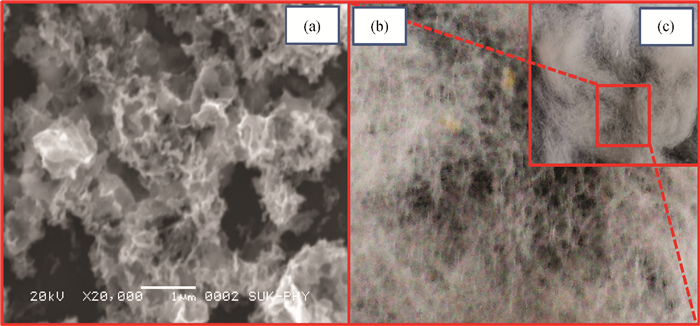
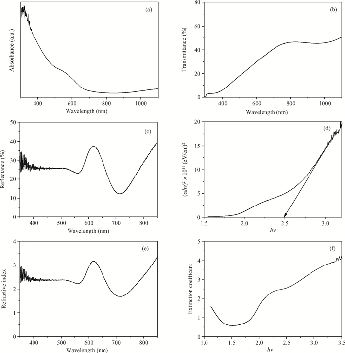
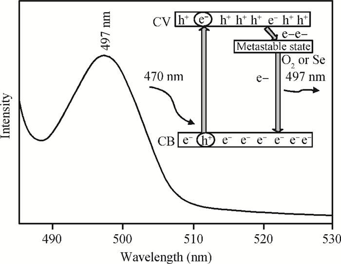
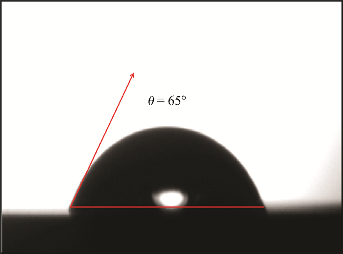
ZnSe thin films are successfully deposited by spray pyrolysis deposition technique. Deposited thin films are characterized by X-ray diffraction study, and it reveals that spray-deposited ZnSe thin films are polycrystalline with hexagonal crystal structure. Surface morphology is carried out by scanning electron microscopy. It shows cotton-like morphology, and optical properties, such as absorbance, transmittance, reflectance, band gap, refractive index, extinction coefficient are studied. Photoluminescence shows strong emission at 497 nm. Also, spray-deposited ZnSe thin films are hydrophilic in nature, which is shown by contact angle meter.
J. Semicond.
2014, 35(11): 113002 doi: 10.1088/1674-4926/35/11/113002
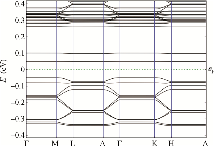
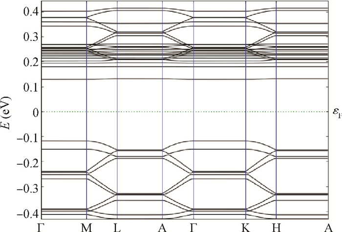
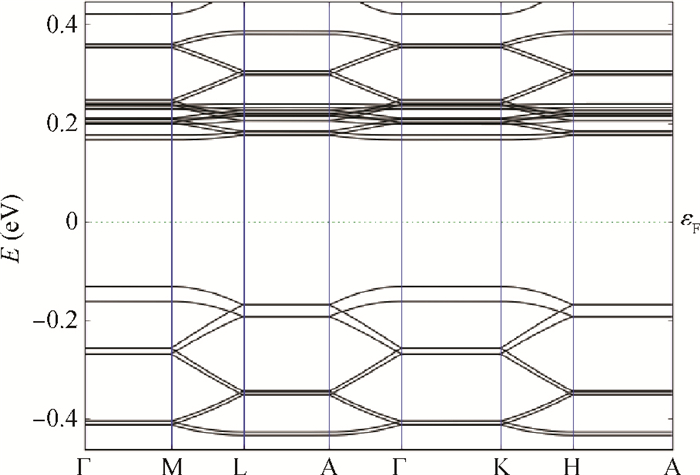
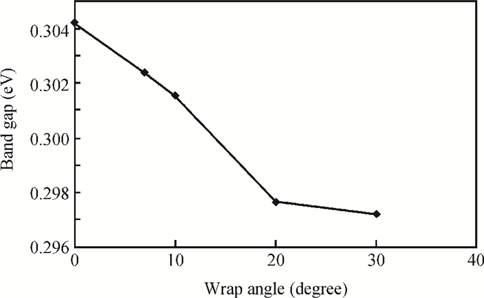
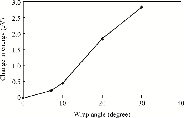
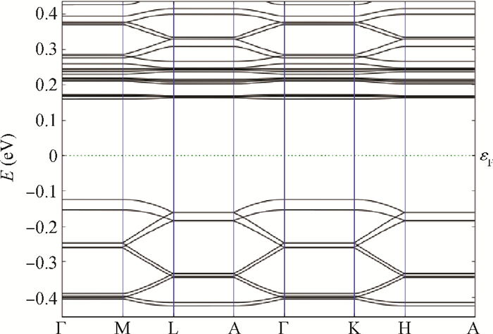
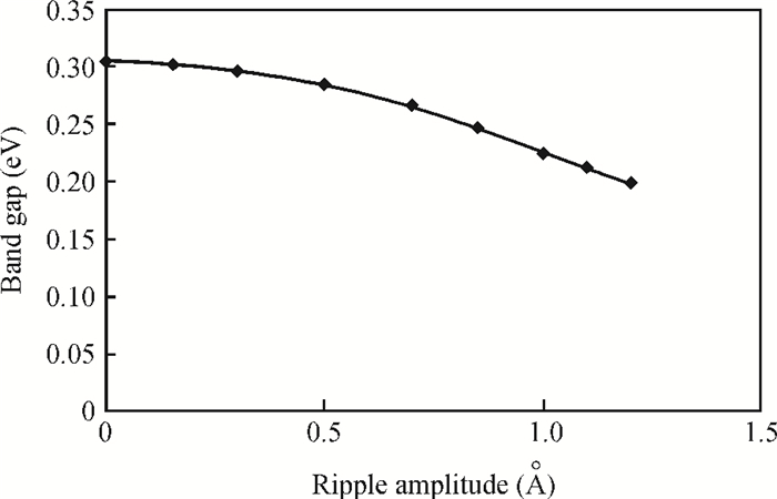
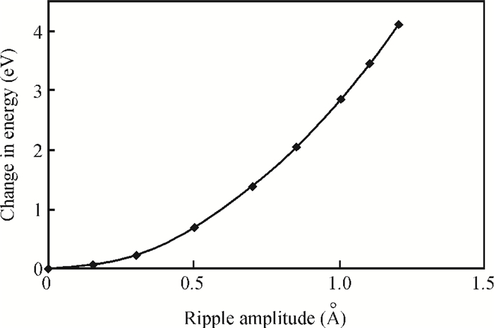
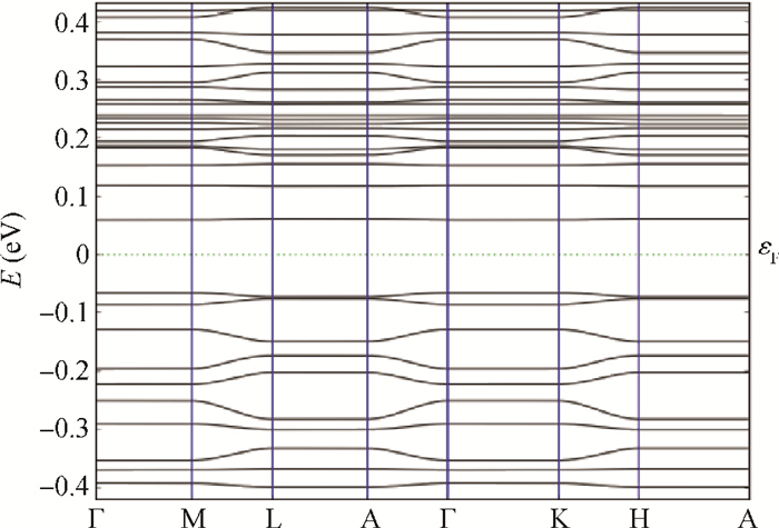
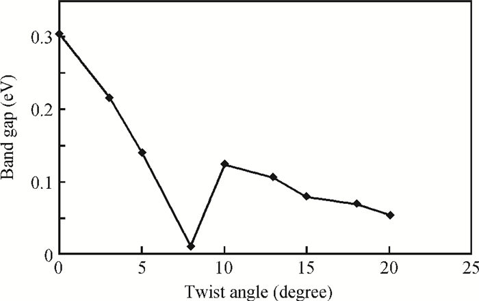
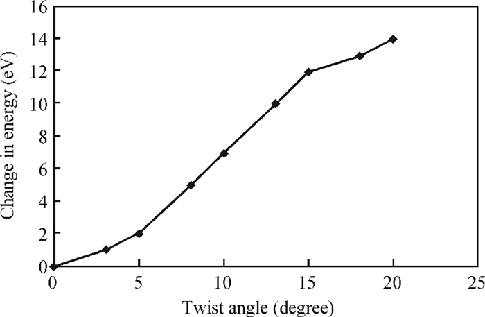
We have investigated the electronic properties of WTe2 armchair nanoribbons with defects. WTe2 nanoribbons can be categorized depending on the edge structure in two types:armchair and zigzag. WTe2 in its bulk form has an indirect band gap but nanoribbons and nanosheets of WTe2 have direct band gaps. Interestingly, the zigzag nanoribbon is metallic while the armchair nanoribbons are semiconducting. Thus they can find applications in device fabrication. Therefore, it is very important to study the effect of defects on the electronic properties of the armchair nanoribbons as these defects can impair the device properties and characteristics. We have considered defects such as:vacancy, rough edge, wrap, ripple and twist in this work. We report the band gap variation with these defects. We have also studied the change in band gap and total energy with varying degrees of wrap, ripple and twist.
J. Semicond.
2014, 35(11): 113003 doi: 10.1088/1674-4926/35/11/113003

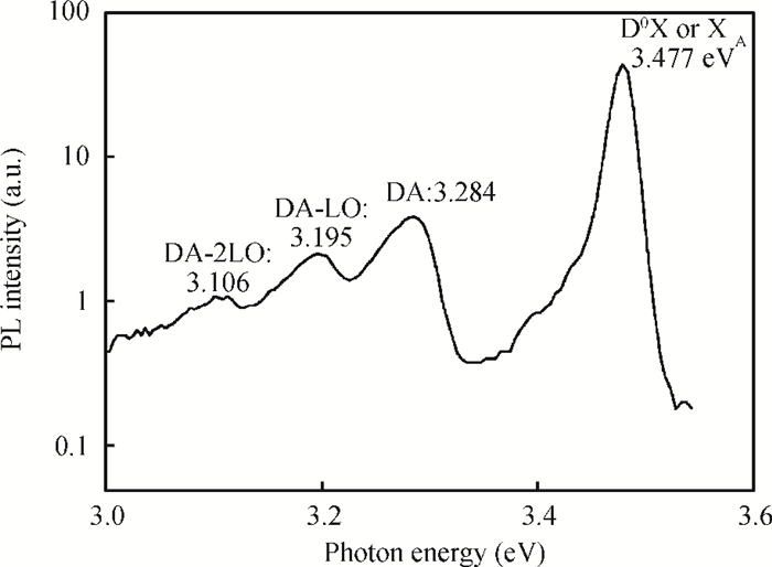
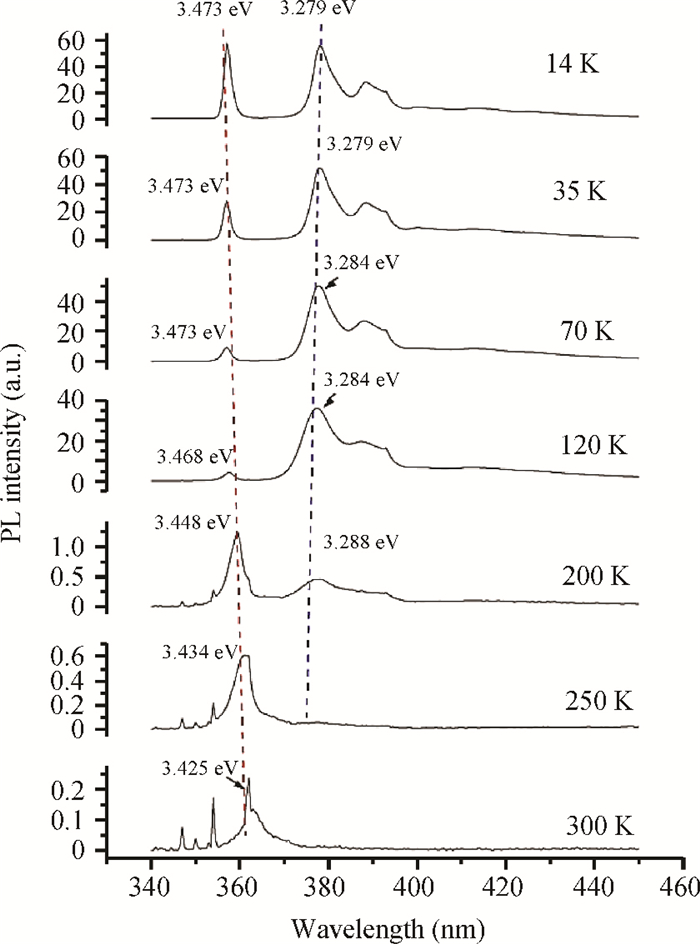
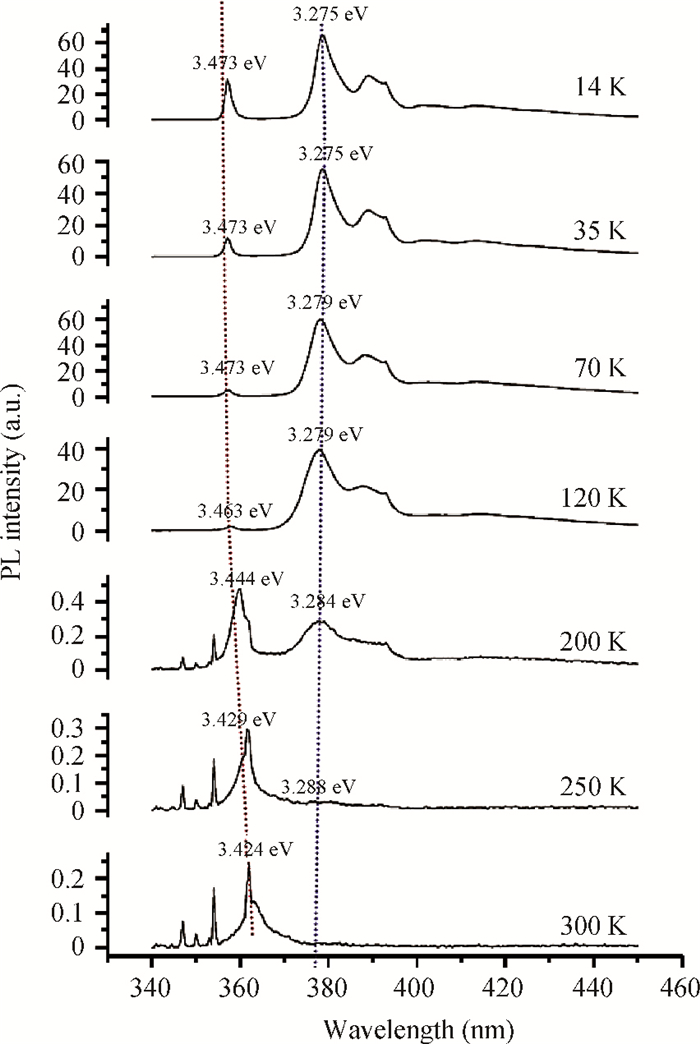
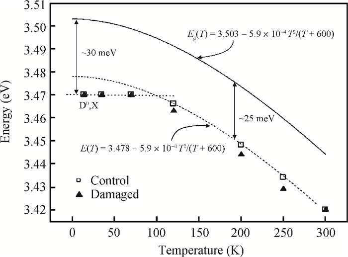
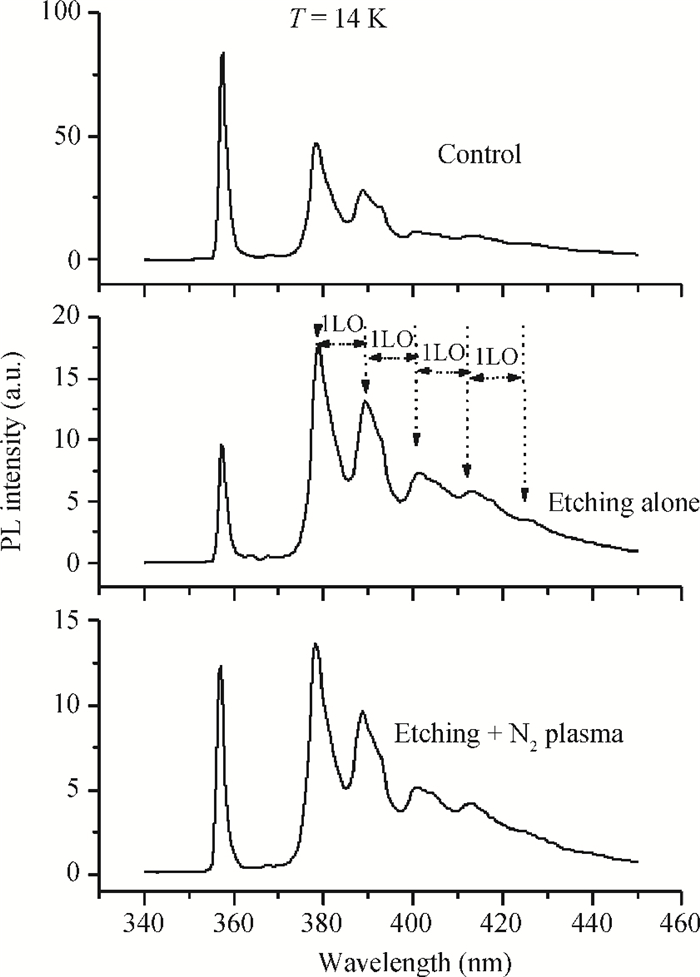
GaN films with reactive ion etching (RIE) induced damage were analyzed using photoluminescence (PL). We observed band-edge as well as donor-acceptor peaks with associated phonon replicas, all in agreement with previous studies. While both the control and damaged samples have their band-edge peak location change with temperature following the Varshni formula, its intensity however decreases with damage while the D-A peak increases considerably. Nitrogen post-etch plasma was shown to improve the band edge peak and decrease the D-A peak. This suggests that the N2 plasma has helped reduce the number of trapped carriers that were participating in the D-A transition and made the D°X transition more active, which reaffirms the N2 post-etch plasma treatment as a good technique to heal the GaN surface, most likely by filling the nitrogen vacancies previously created by etch damage.


J. Semicond.
2014, 35(11): 113004 doi: 10.1088/1674-4926/35/11/113004
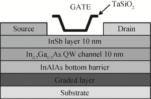
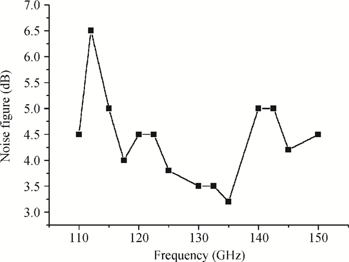
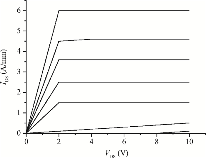
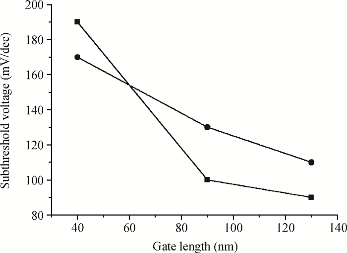
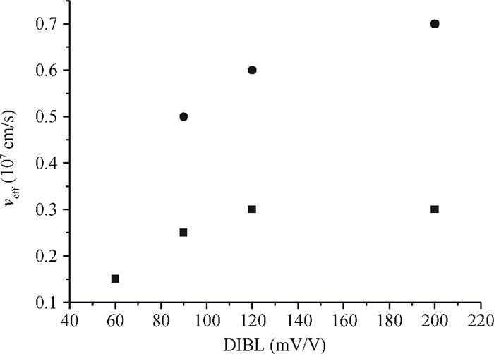
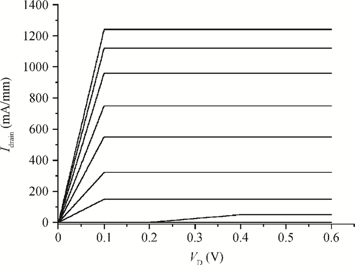
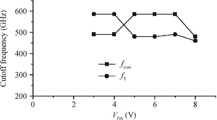
We report on an indium antimonide high electron mobility transistor with record cut-off frequency characteristics. For high frequency response it is important to minimize parasitic resistance and capacitance to improve short-channel effects. For analog applications adequate pinch-off behavior is demonstrated. For proper device scaling we need high electron mobility and high electron density. Toward this end, the device design features and simulation are carried out by the Synopsys TCAD tool. A 30 nm InSb HEMT exhibits an excellent cut-off frequency of 586 GHz. To the knowledge of the authors, the obtained cut-off frequency is the highest ever reported in any FET on any material system.
J. Semicond.
2014, 35(11): 113005 doi: 10.1088/1674-4926/35/11/113005
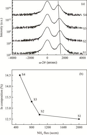
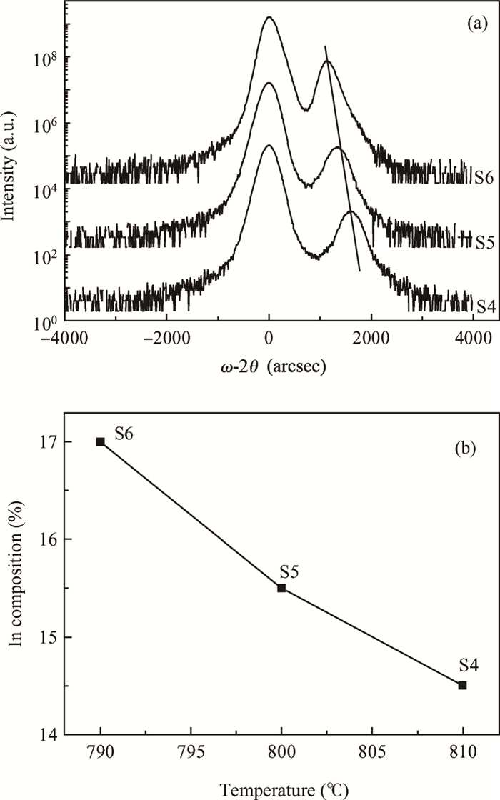
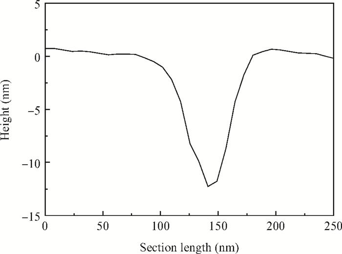
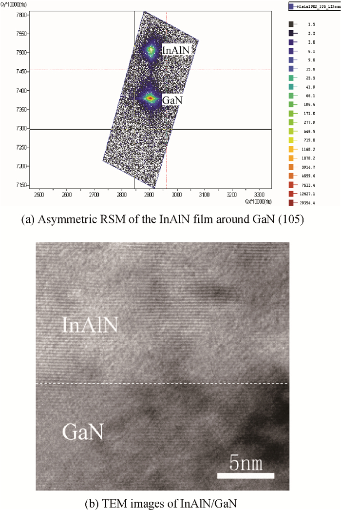
InAlN/GaN heterostructures were grown on sapphire substrates by low-pressure metal organic chemical vapor deposition. The influences of NH3 flux and growth temperature on the In composition and morphologies of the InAlN were investigated by X-ray diffraction and atomic force microscopy. It's found that the In composition increases quickly with NH3 flux decrease. But it's not sensitive to NH3 flux under higher flux. This suggests that lower NH3 flux induces a higher growth rate and an enhanced In incorporation. The In composition also increases with the growth temperatures decreasing, and the defects of the InAlN have close relation with In composition. Unstrained InAlN with In composition of 17% is obtained at NH3 flux of 500 sccm and growth temperature of 790℃. The InAlN/GaN heterostructure high electron mobility transistor sample showed a high two-dimensional electron gas (2DEG) mobility of 1210 cm2/(V·s) with the sheet density of 2.3×1013 cm-2 at room temperature.


J. Semicond.
2014, 35(11): 113006 doi: 10.1088/1674-4926/35/11/113006
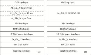
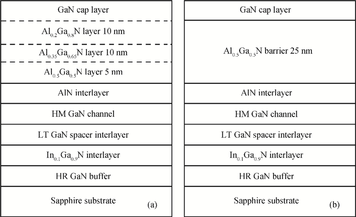
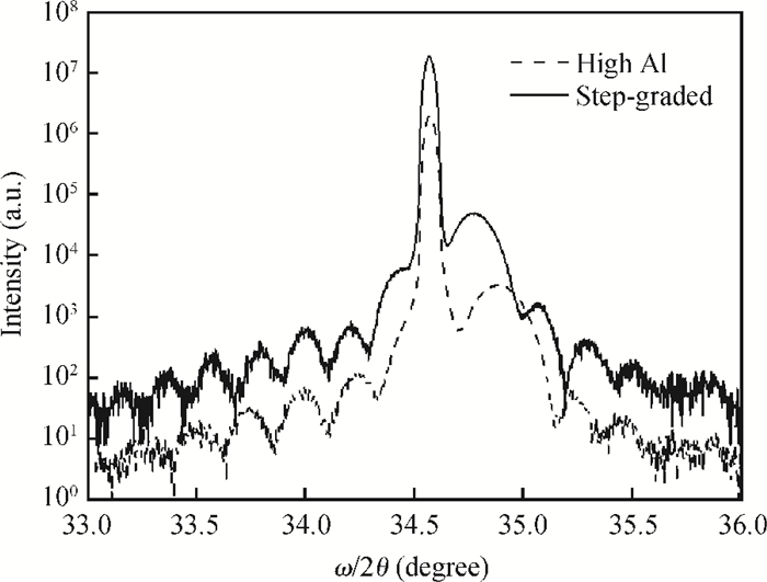
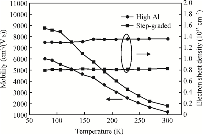
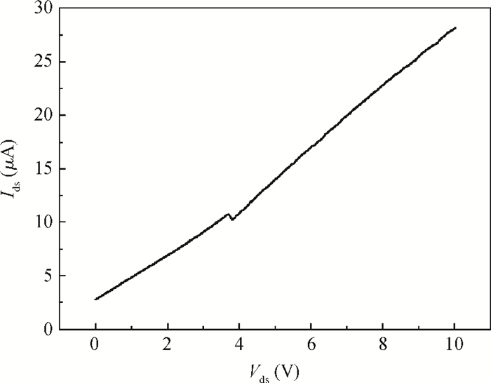
A novel InGaN back barrier high electron mobility transistors structure with a compositionally step-graded AlGaN barrier layer was grown by metal organic chemical vapor deposition on sapphire substrate. The structural and electrical properties of two samples were investigated and compared:the first sample is the step-graded structure and the second one is the high Al structure as a comparison. By calculating full width at half maximum of XRD measurements, the densities of screw-type threading dislocations are 8.34×108 cm-2 and 11.44×108 cm-2 for step-graded structure and high Al structure, respectively, which are consistent with the results of atomic force microscopy. By Hall measurements, the measured two-dimensional electron gas mobility was 1820 cm2/(V·s) for step-graded structure, and 1300 cm2/(V·s) for high Al structure, respectively. The step-graded structure improves the crystal quality of AlGaN layer due to the released lattice strain. The device was fabricated and leakage current is only 28 μA when the drain voltage is 10 V; it was found that the InGaN back barrier could effectively reduce the buffer leakage current.
J. Semicond.
2014, 35(11): 114001 doi: 10.1088/1674-4926/35/11/114001
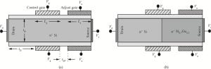
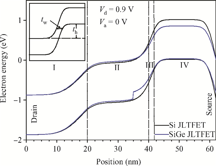
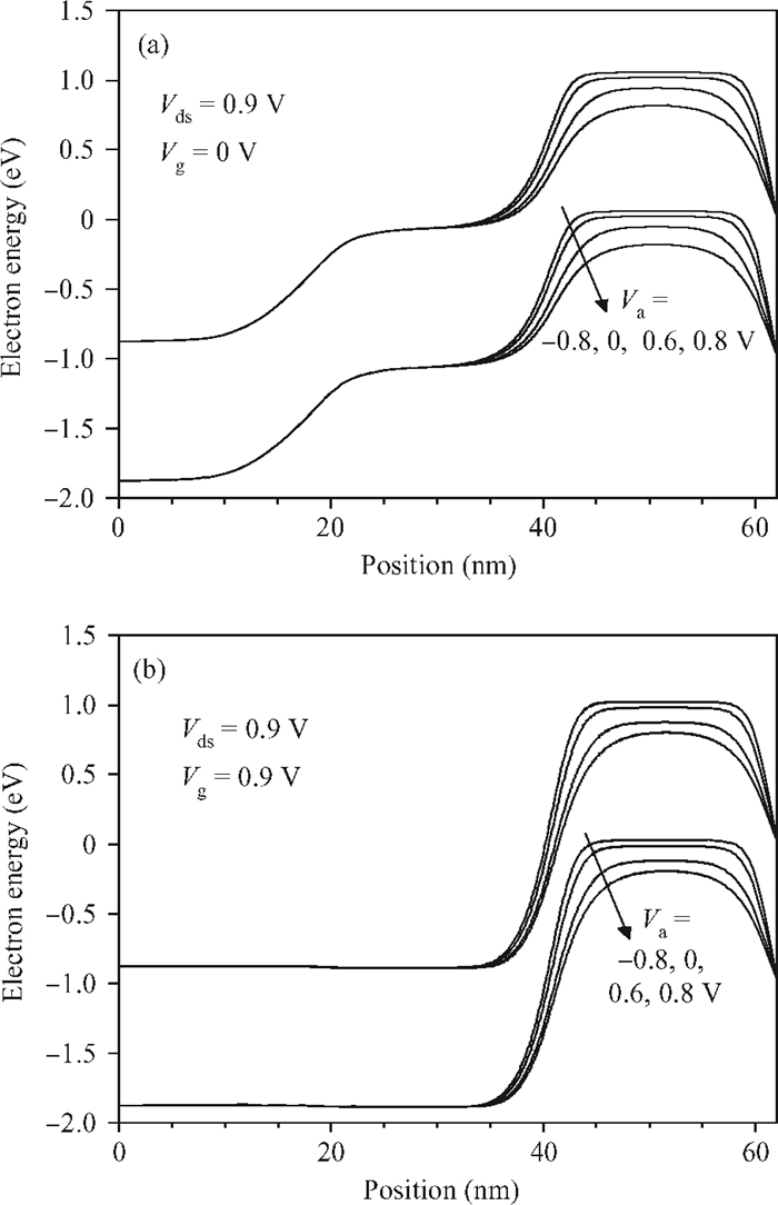
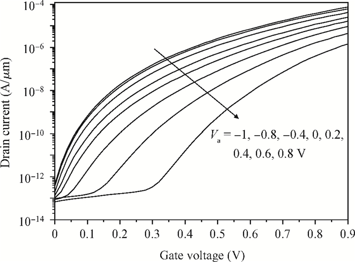
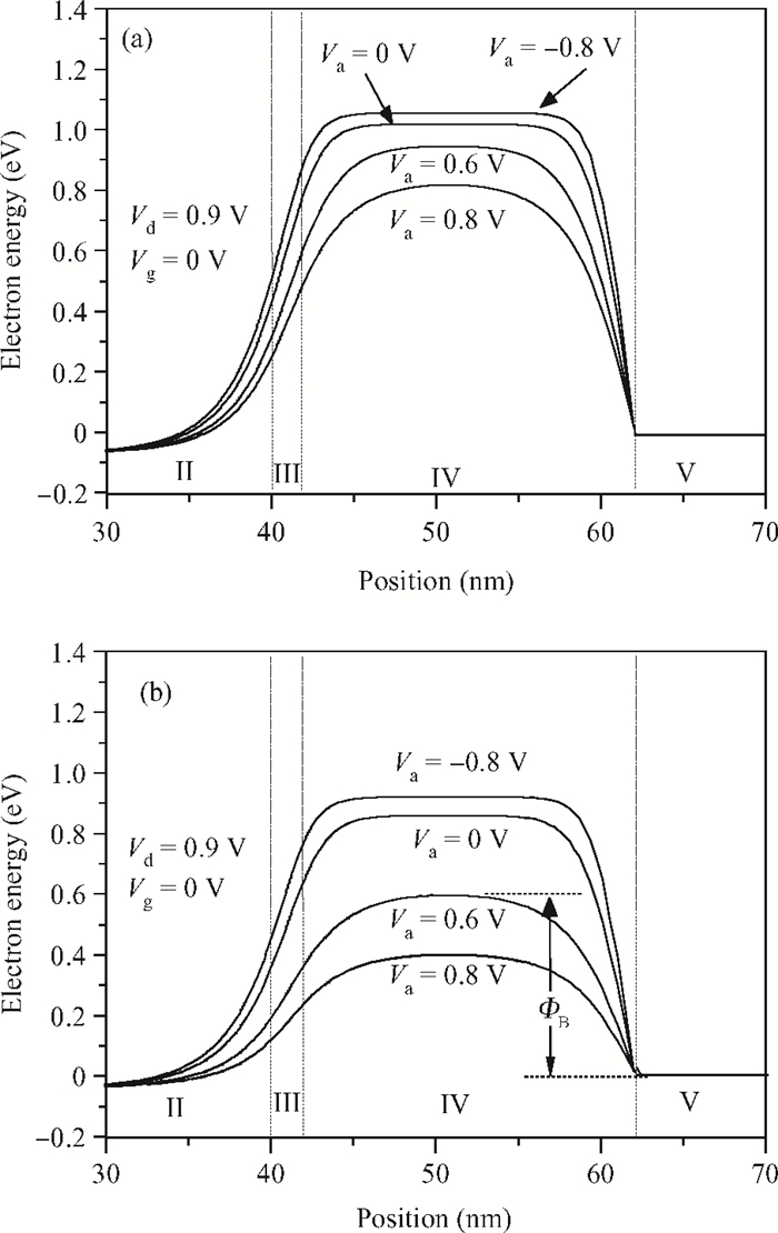
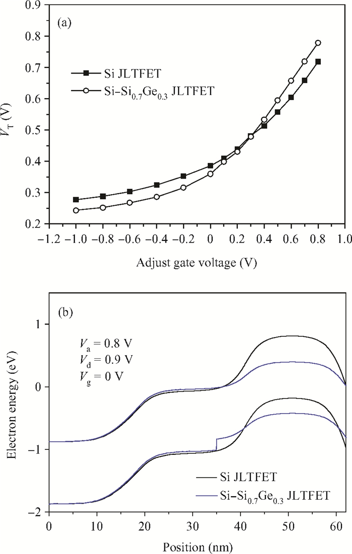
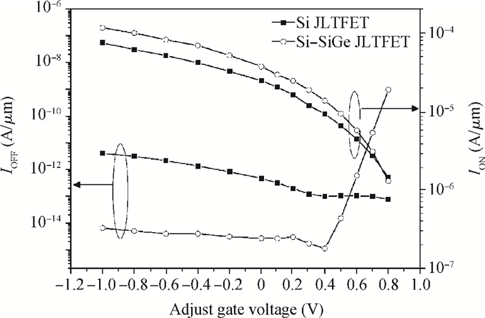
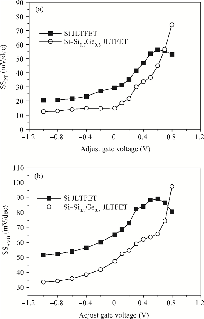
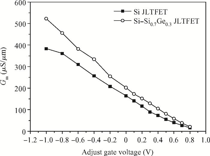
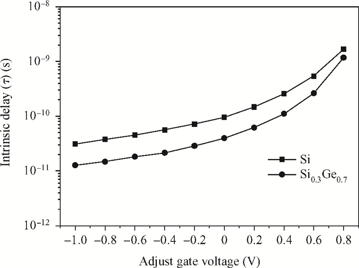
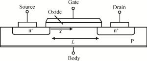
We propose a dynamic threshold voltage junctionless tunnel FET (DT-JLTFET) in which the threshold voltage can be dynamically adjusted, resulting in higher ON-current. Through 2D numerical simulations, it is presented that the threshold voltage in the DT-JLTFET can be adjusted by applying a voltage to the adjust gate. The impact of the threshold voltage shift on the overall performance of the device is also studied. A comparison is made between the dynamic threshold voltage characteristics of a silicon JLTFET and a Si0.7Ge0.3 source JLTFET.


J. Semicond.
2014, 35(11): 114002 doi: 10.1088/1674-4926/35/11/114002
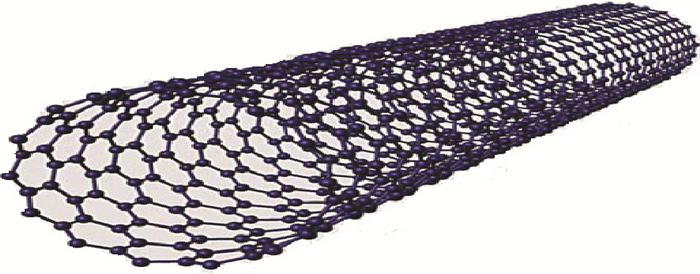
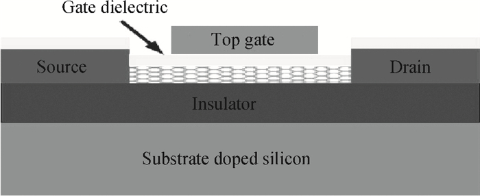
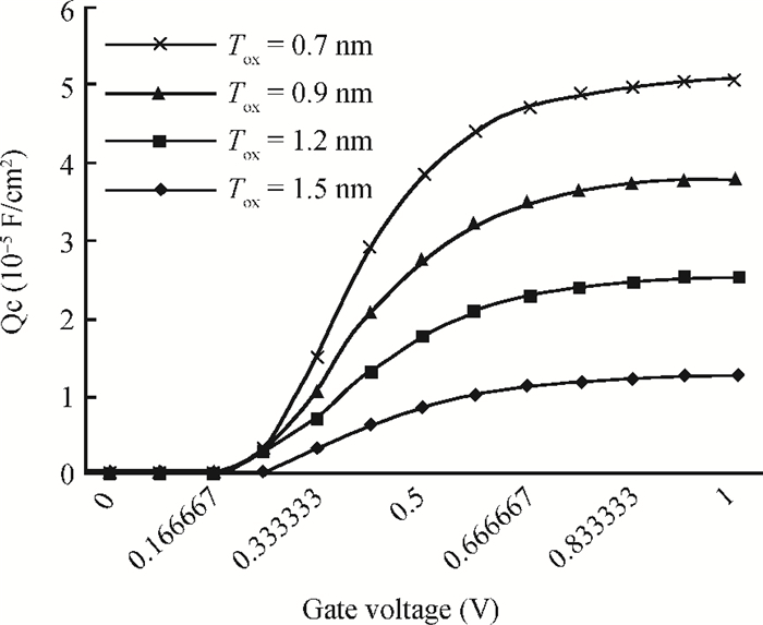
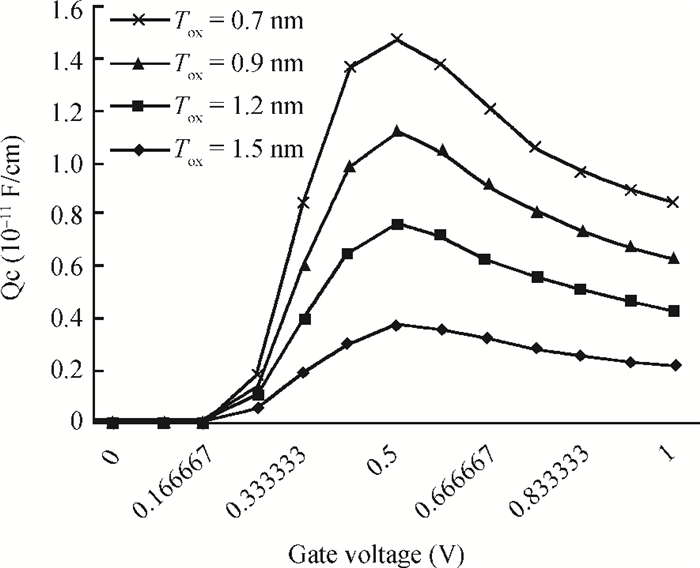
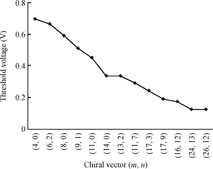
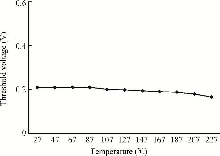
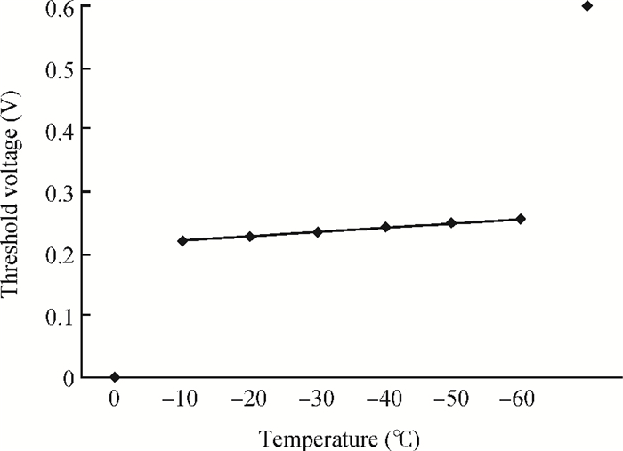
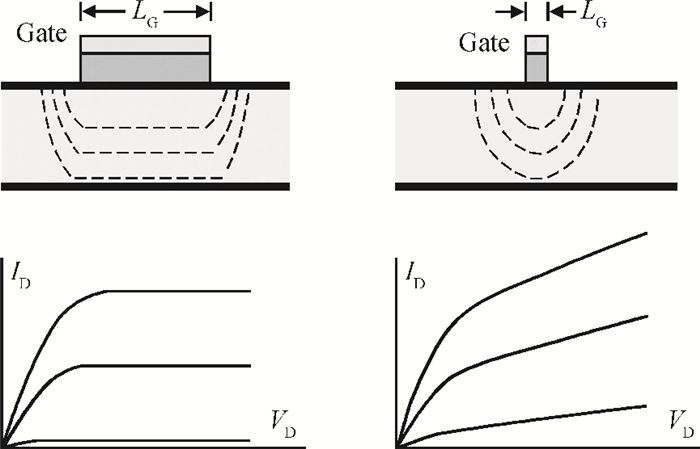
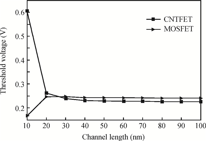
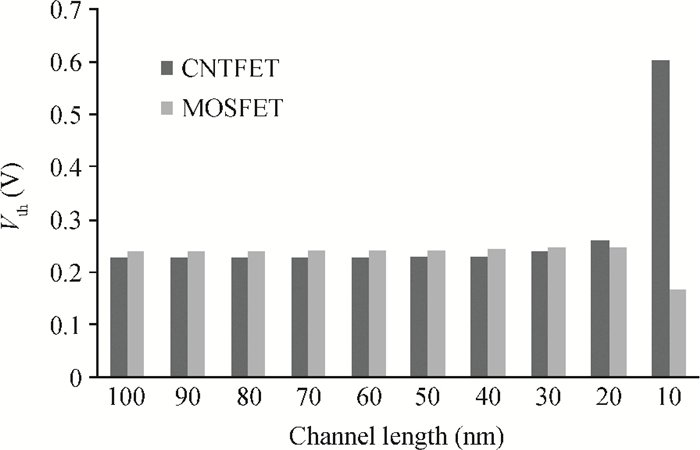
A comparison of the CNTFET device with the MOSFET device in the nanometer regime is reported. The characteristics of both devices are observed as varying the oxide thickness.Thereafter, we have analyzed the effect of the chiral vector and the temperature on the threshold voltage of the CNTFET device.After simulation on the HSPICE tool, we observed that the high threshold voltage can be achieved at a low chiral vector pair.It is also observed that the effect of temperature on the threshold voltage of the CNTFET is negligibly small.After that, we have analyzed the channel length variation and their impact on the threshold voltage of the CNTFET as well as MOSFET devices.We found an anomalous effect from our simulation result that the threshold voltage increases with decreasing the channel length in CNTFET devices; this is contrary to the well known short channel effect. It is observed that at below the 10 nm channel length, the threshold voltage is increased rapidly in the case of the CNTFET device, whereas in the case of the MOSFET device, the threshold voltage decreases drastically.


J. Semicond.
2014, 35(11): 114003 doi: 10.1088/1674-4926/35/11/114003
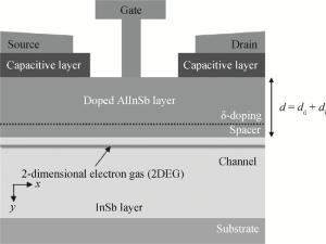
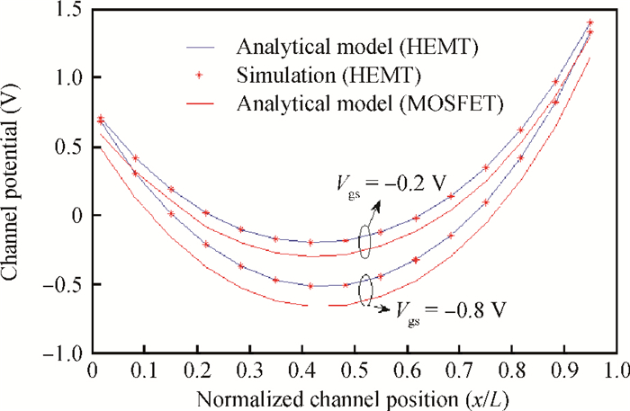
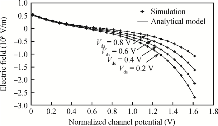
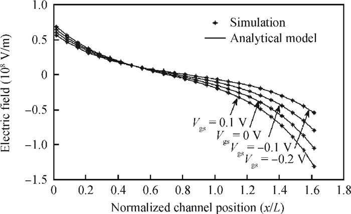
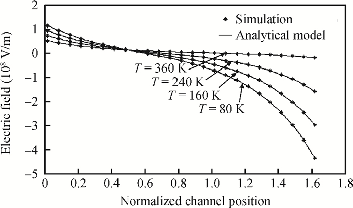
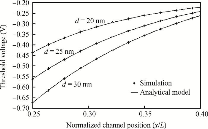
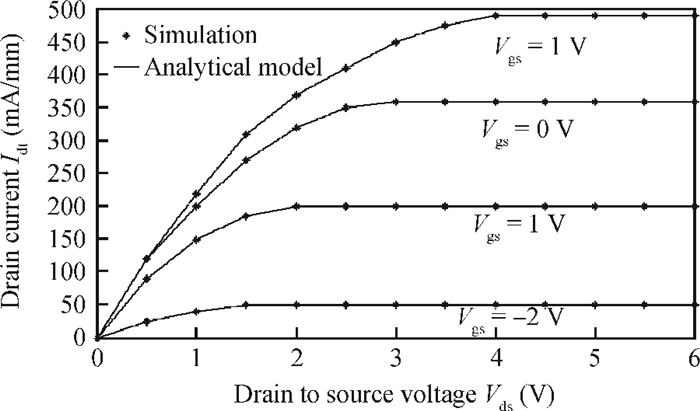
We have developed a 2D analytical model for the single gate AlInSb/InSb HEMT device by solving the Poisson equation using the parabolic approximation method. The developed model analyses the device performance by calculating the parameters such as surface potential, electric field distribution and drain current. The high mobility of the AlInSb/InSb quantum makes this HEMT ideal for high frequency, high power applications. The working of the single gate AlInSb/InSb HEMT device is studied by considering the variation of gate source voltage, drain source voltage, and channel length under the gate region and temperature. The carrier transport efficiency is improved by uniform electric field along the channel and the peak values near the source and drain regions. The results from the analytical model are compared with that of numerical simulations (TCAD) and a good agreement between them is achieved.


J. Semicond.
2014, 35(11): 114004 doi: 10.1088/1674-4926/35/11/114004
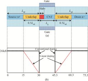
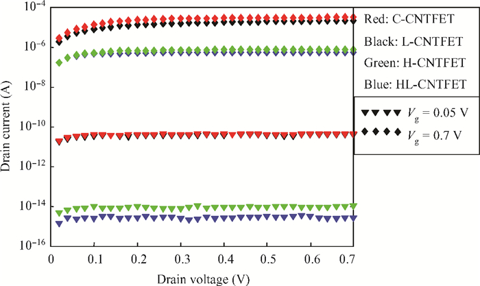
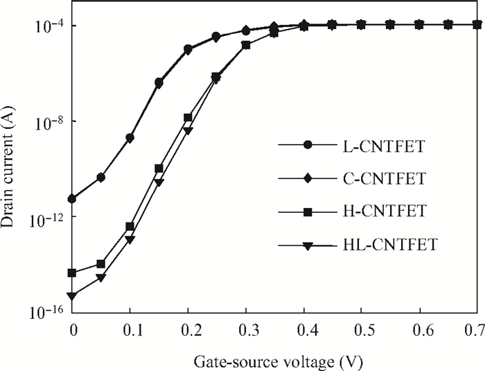
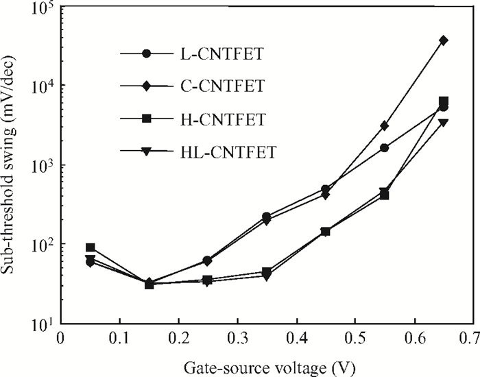
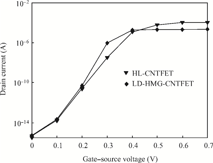
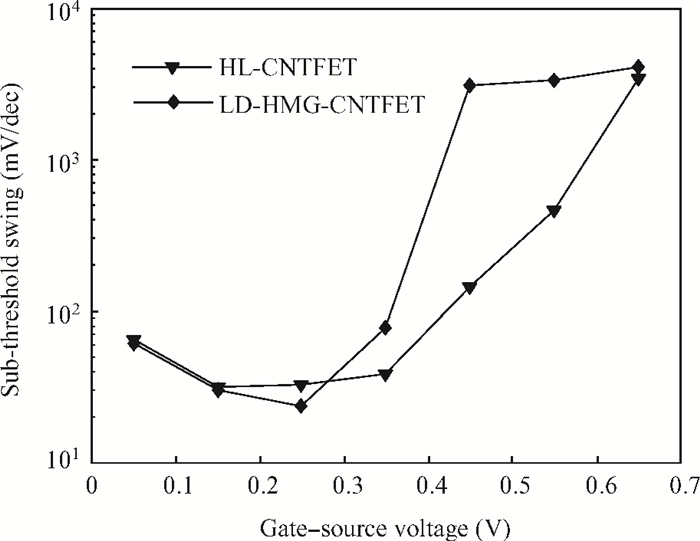
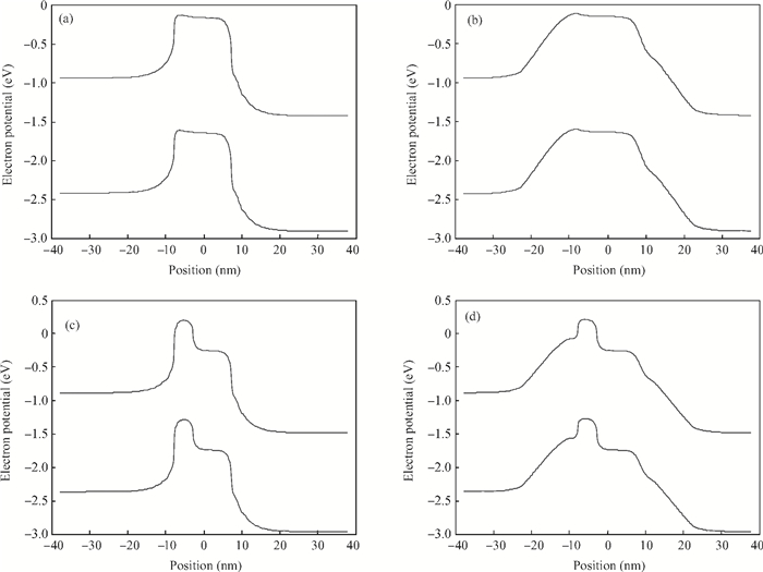
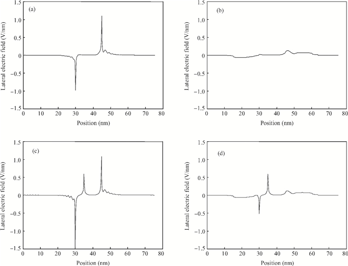
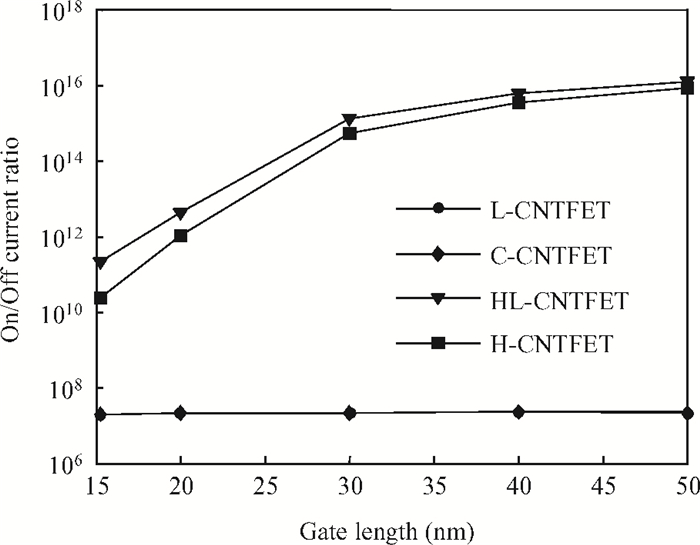
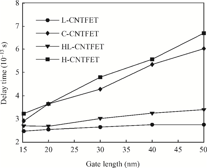
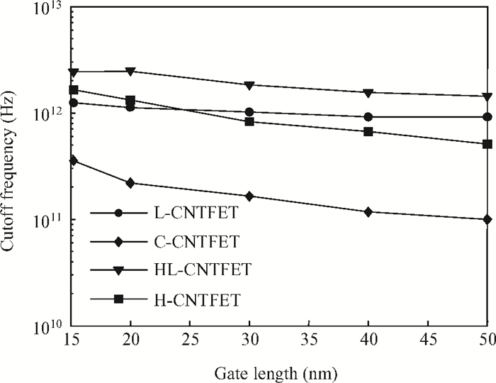
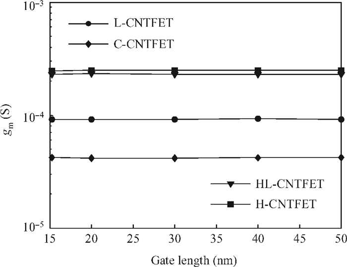
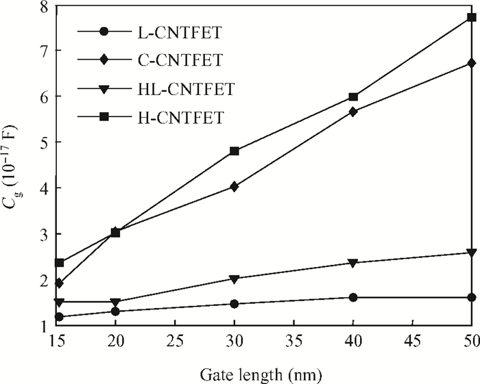
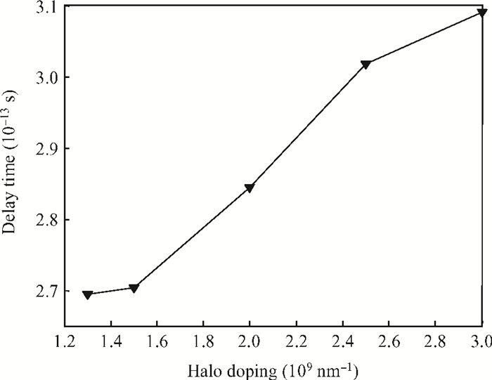
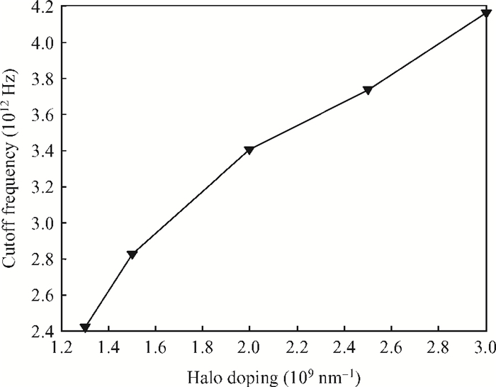
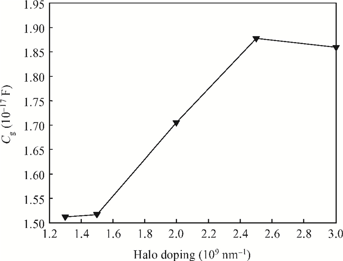
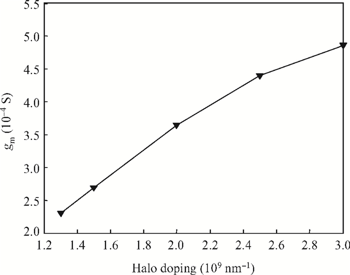
To overcome short-channel effects (SCEs) in high-performance device applications, a novel structure of CNTFET with a combination of halo and linear doping structure (HL-CNTFET) has been proposed. It has been theoretically investigated by a quantum kinetic model, which is based on two-dimensional non-equilibrium Green's functions solved self-consistently with Poisson's equations. We have studied the effect of halo doping and linear doping structure on static and dynamical performances of HL-CNTFET. It is demonstrated that a halo doping structure can decrease the drain leakage current and improve the on/off current ratio, and that linear doping can improve high-frequency and switching performance.

J. Semicond.
2014, 35(11): 114005 doi: 10.1088/1674-4926/35/11/114005
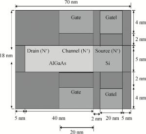
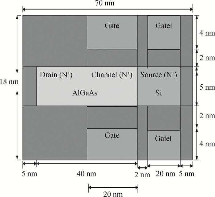
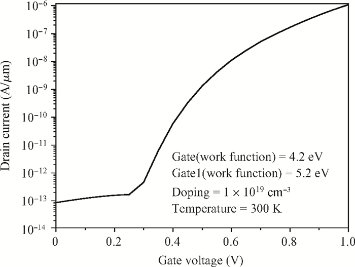
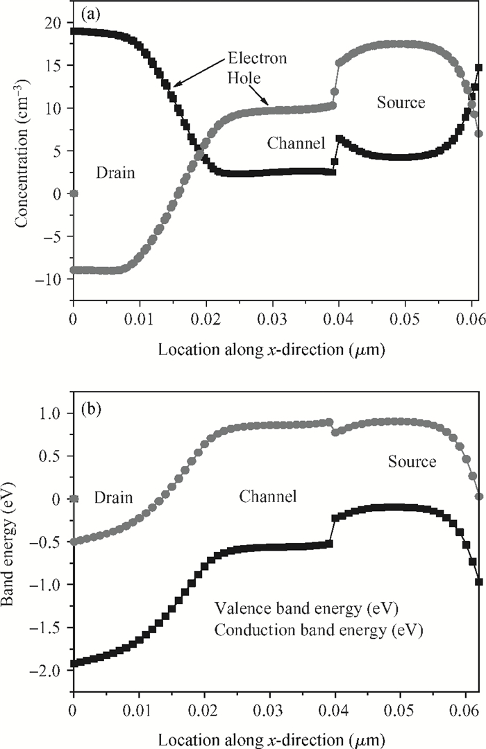
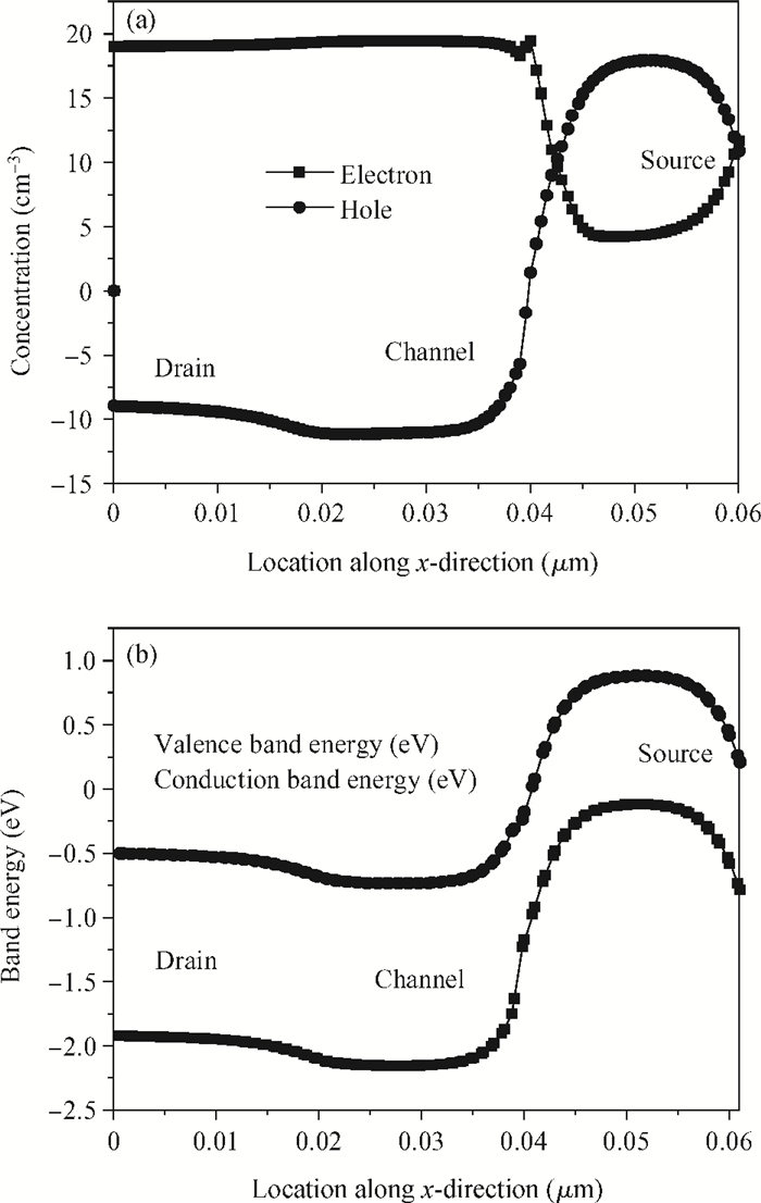
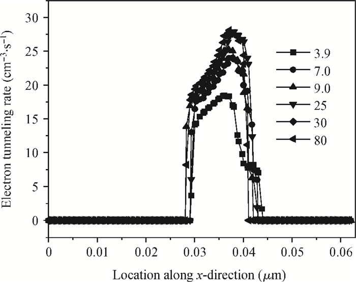
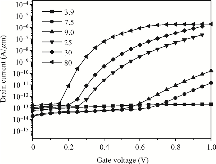
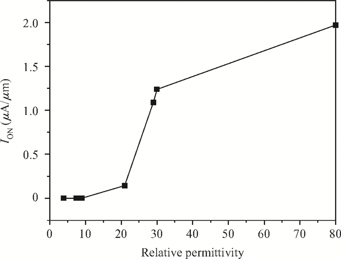
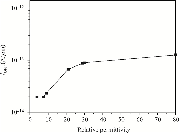
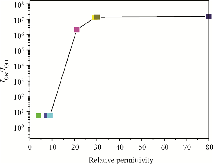
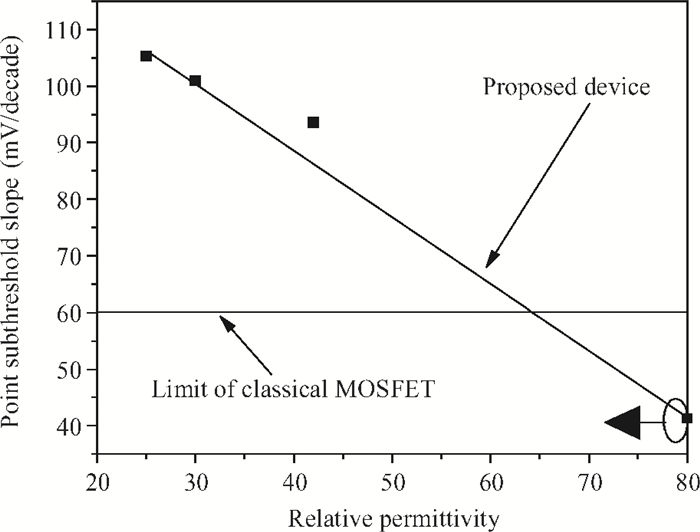
We propose a heterostructure junctionless tunnel field effect transistor (HJL-TFET) using AlGaAs/Si. In the proposed HJL-TFET, low band gap silicon is used in the source side and higher band gap AlGaAs in the drain side. The whole AlGaAs/Si region is heavily doped n-type. The proposed HJL-TFET uses two isolated gates (named gate, gate1) with two different work functions (gate=4.2 eV, gate1=5.2 eV respectively). The 2-D nature of HJL-TFET current flow is studied. The proposed structure is simulated in Silvaco with different gate dielectric materials. This structure exhibits a high on current in the range of 1.4×10⁻⁶ A/μm, the off current remains as low as 9.1×10⁻¹⁴ A/μm. So ION/IOFF ratio of ≃ 108 is achieved. Point subthreshold swing has also been reduced to a value of ≃ 41 mV/decade for TiO2 gate material.
J. Semicond.
2014, 35(11): 114006 doi: 10.1088/1674-4926/35/11/114006
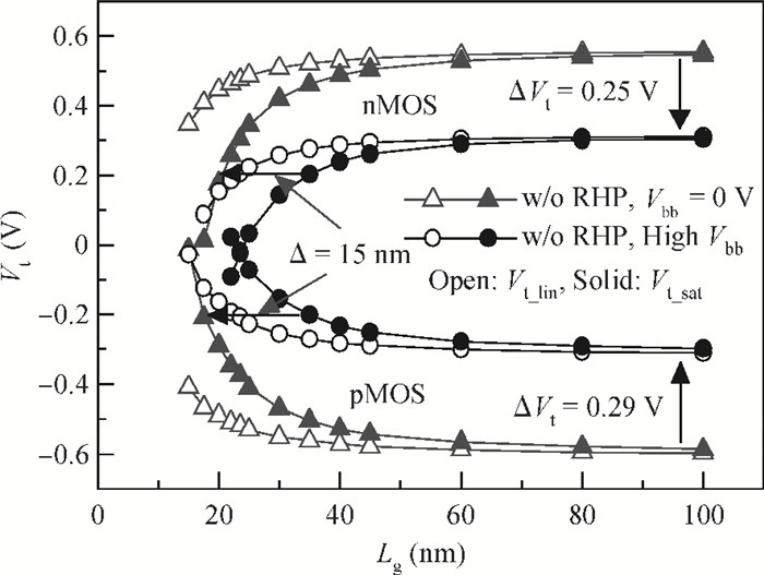
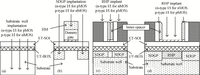
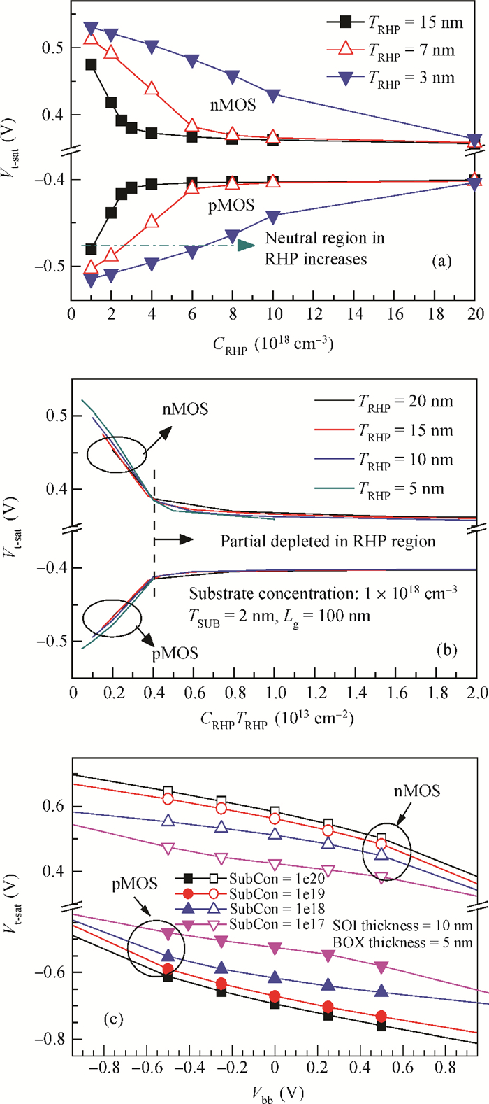
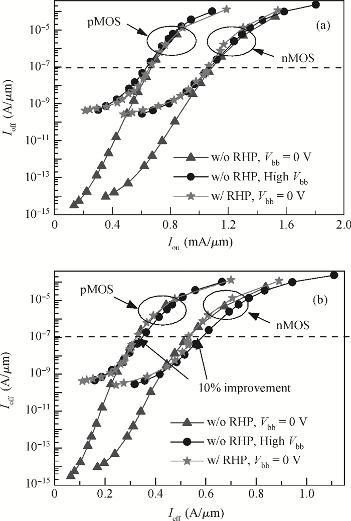
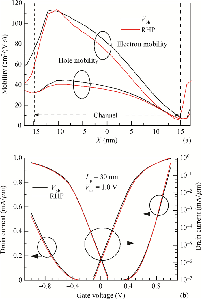
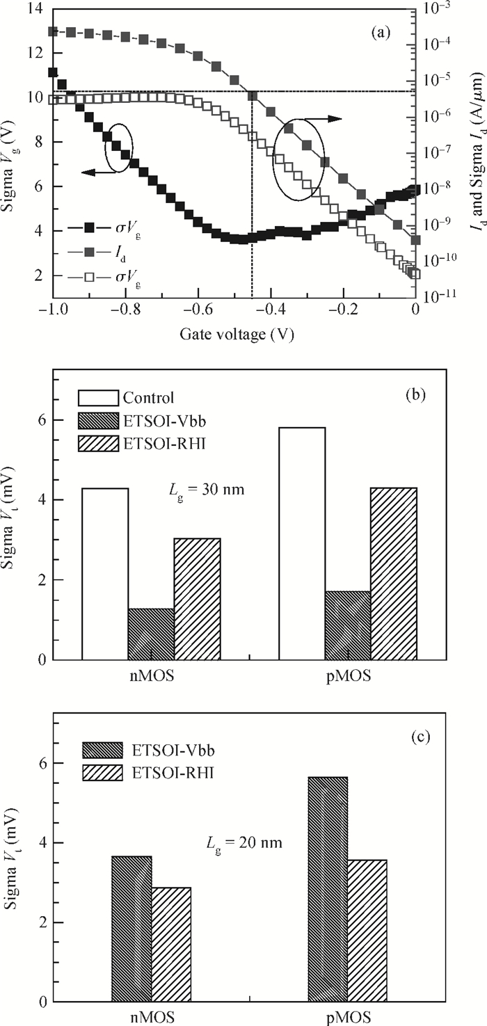
The importance of substrate doping engineering for extremely thin SOI MOSFETs with ultra-thin buried oxide (ES-UB-MOSFETs) is demonstrated by simulation. A new substrate/backgate doping engineering, lateral non-uniform dopant distributions (LNDD) is investigated in ES-UB-MOSFETs. The effects of LNDD on device performance, Vt-roll-off, channel mobility and random dopant fluctuation (RDF) are studied and optimized. Fixing the long channel threshold voltage (Vt) at 0.3 V, ES-UB-MOSFETs with lateral uniform doping in the substrate and forward back bias can scale only to 35 nm, meanwhile LNDD enables ES-UB-MOSFETs to scale to a 20 nm gate length, which is 43% smaller. The LNDD degradation is 10% of the carrier mobility both for nMOS and pMOS, but it is canceled out by a good short channel effect controlled by the LNDD. Fixing Vt at 0.3 V, in long channel devices, due to more channel doping concentration for the LNDD technique, the RDF in LNDD controlled ES-UB-MOSFETs is worse than in back-bias controlled ES-UB-MOSFETs, but in the short channel, the RDF for LNDD controlled ES-UB-MOSFET is better due to its self-adaption of substrate doping engineering by using a fixed thickness inner-spacer. A novel process flow to form LNDD is proposed and simulated.


J. Semicond.
2014, 35(11): 114007 doi: 10.1088/1674-4926/35/11/114007
The advantages of InGaN/GaN light emitting diodes (LEDs) with p-GaN grown under high pressures are studied. It is shown that the high growth pressure could lead to better electronic properties of p-GaN layers due to the eliminated compensation effect. The contact resistivity of p-GaN layers are decreased due to the reduced donor-like defects on the p-GaN surface. The leakage current is also reduced, which may be induced by the better filling of V-defects with p-GaN layers grown under high pressures. The LED efficiency thus could be enhanced with high pressure grown p-GaN layers.

J. Semicond.
2014, 35(11): 114008 doi: 10.1088/1674-4926/35/11/114008

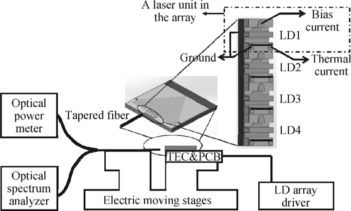
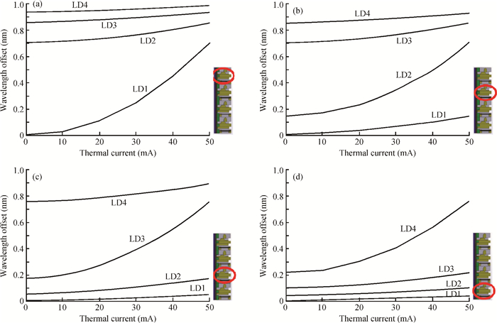
Four-channel monolithically integrated index-coupled distributed-feedback laser array has been fabricated using nanoimprint technology for 1.3 μm CWDM system. Selective lasing wavelength with 20 nm wavelength space is obtained. The present results show that the nanoimprint technology is mature and reliable in the fabrication of DFB laser array.


J. Semicond.
2014, 35(11): 114009 doi: 10.1088/1674-4926/35/11/114009
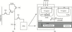
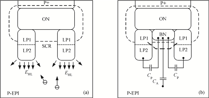
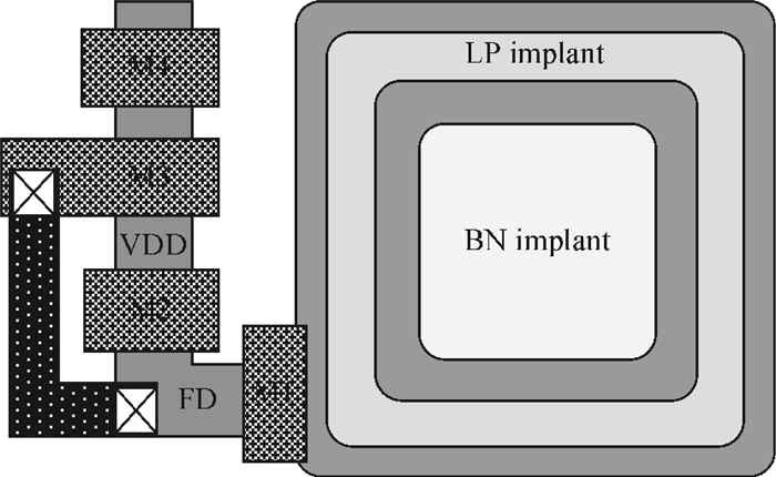
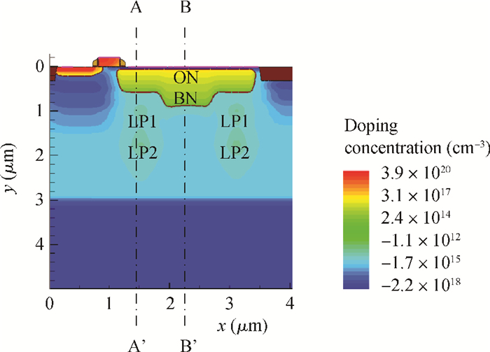
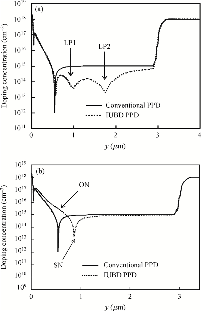
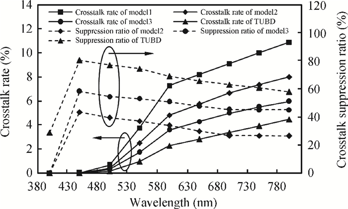
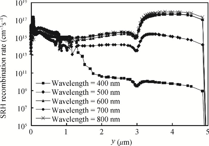
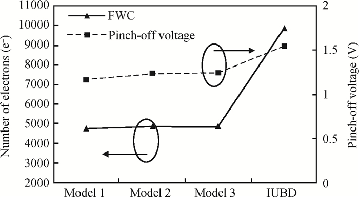
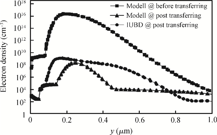
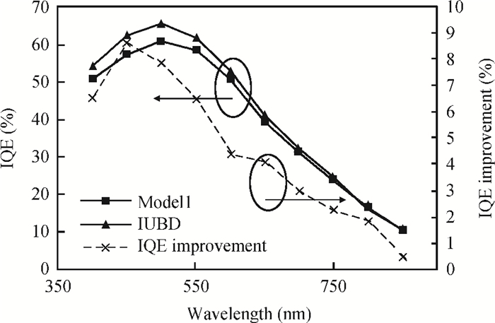
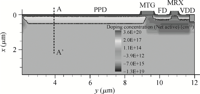
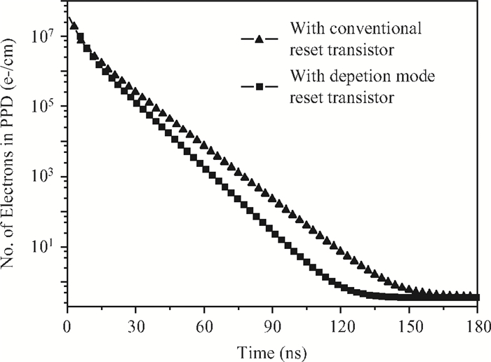
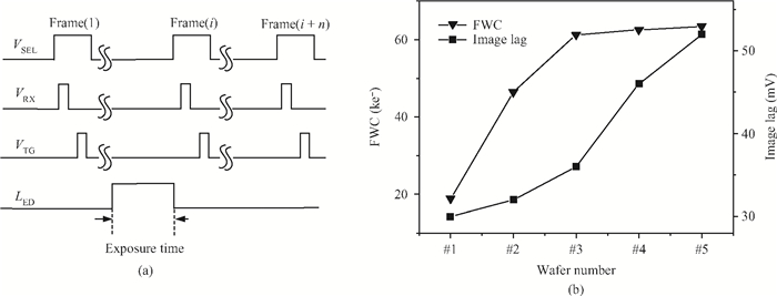
A design of an inverse U-shape buried doping in a pinned photodiode (PPD) of CMOS image sensors is proposed for electrical crosstalk suppression between adjacent pixels. The architecture achieves no extra fill factor consumption, and proper built-in electric fields can be established according to the doping gradient created by the injections of the extremely low P-type doping buried regions in the epitaxial layer, causing the excess electrons to easily drift back to the photosensitive area rarely with a diffusion probability; the overall junction capacitance and photosensitive area extensions for a full well capacity (FWC) and internal quantum efficiency (IQE) improving are achieved by the injection of a buried N-type doping. By considering the image lag issue, the process parameters of all the injections have been precisely optimized. Optical simulation results based on the finite difference time domain method show that compared to the conventional PPD, the electrical crosstalk rate of the proposed architecture can be decreased by 60%-80% at an incident wavelength beyond 450 nm, IQE can be clearly improved at an incident wavelength between 400 and 600 nm, and the FWC can be enhanced by 107.5%. Furthermore, the image lag performance is sustained to a perfect low level. The present study provides important guidance on the design of ultra high resolution image sensors.

J. Semicond.
2014, 35(11): 114010 doi: 10.1088/1674-4926/35/11/114010

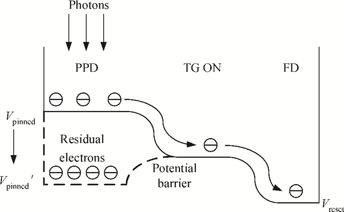
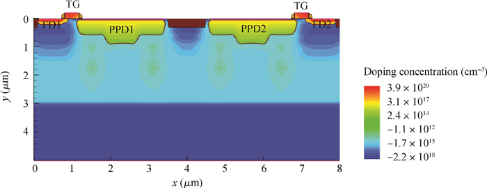
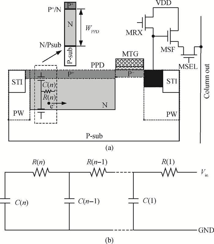
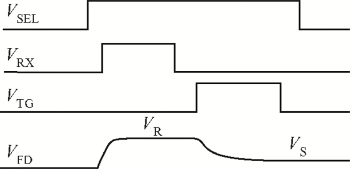
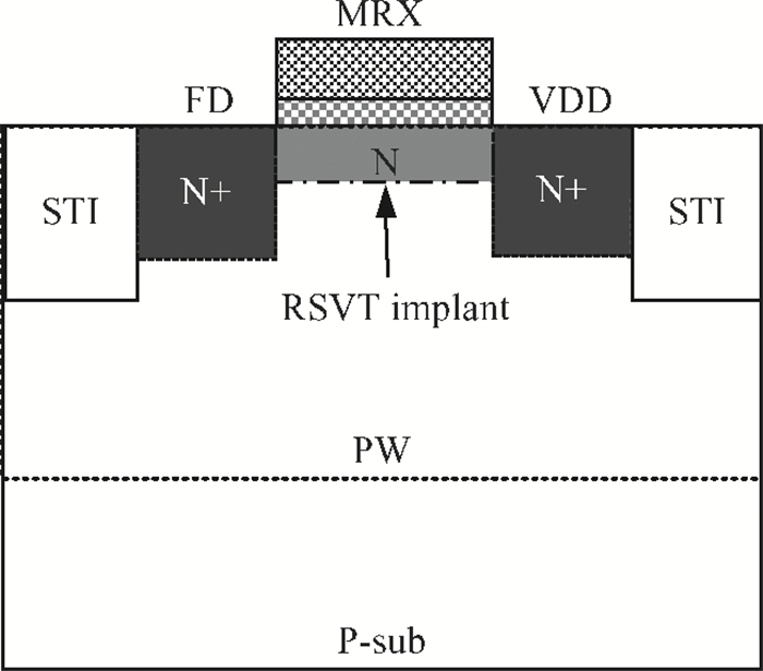
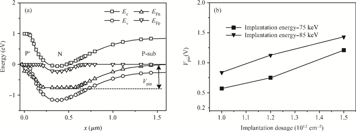
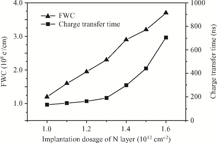
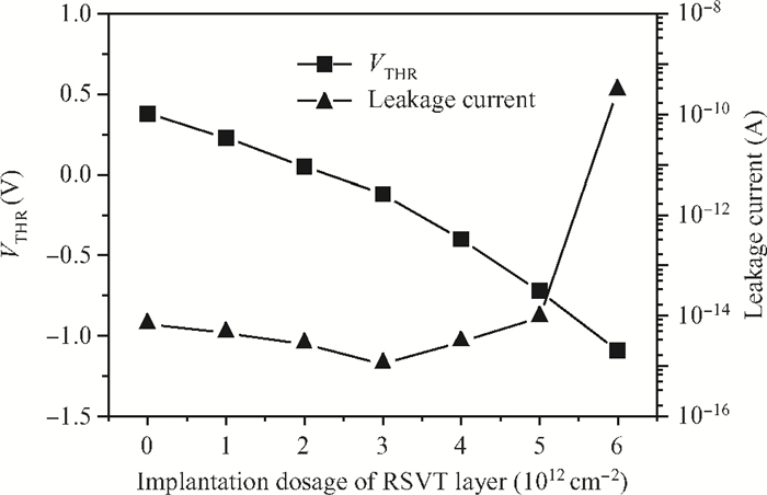
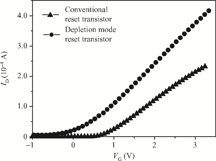
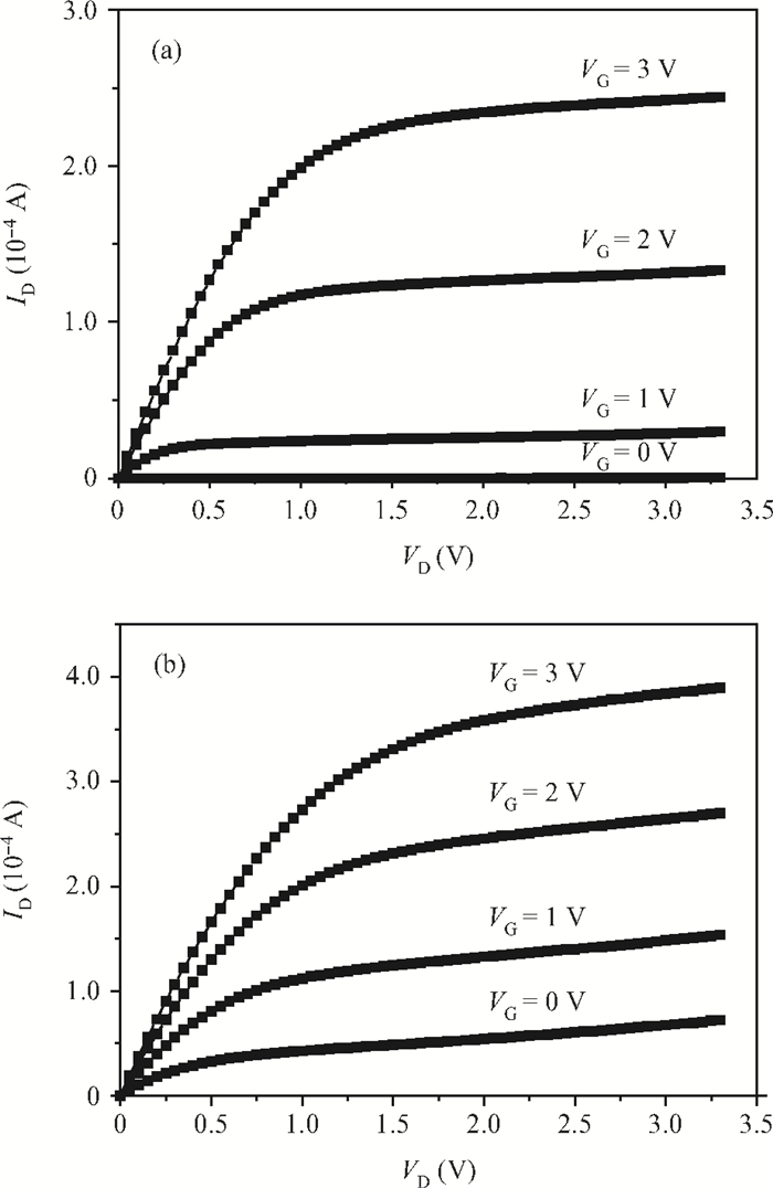
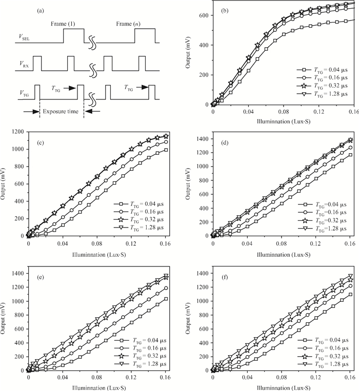
This paper proposes pixel process techniques to reduce the charge transfer time in high speed CMOS image sensors. These techniques increase the lateral conductivity of the photo-generated carriers in a pinned photodiode (PPD) and the voltage difference between the PPD and the floating diffusion (FD) node by controlling and optimizing the N doping concentration in the PPD and the threshold voltage of the reset transistor, respectively. The techniques shorten the charge transfer time from the PPD diode to the FD node effectively. The proposed process techniques do not need extra masks and do not cause harm to the fill factor. A sub array of 32×64 pixels was designed and implemented in the 0.18 μm CIS process with five implantation conditions splitting the N region in the PPD. The simulation and measured results demonstrate that the charge transfer time can be decreased by using the proposed techniques. Comparing the charge transfer time of the pixel with the different implantation conditions of the N region, the charge transfer time of 0.32 μs is achieved and 31% of image lag was reduced by using the proposed process techniques.

J. Semicond.
2014, 35(11): 115001 doi: 10.1088/1674-4926/35/11/115001
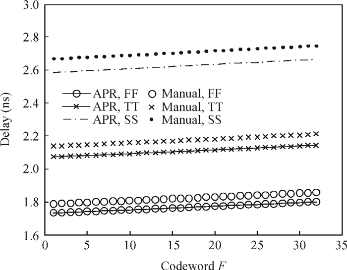
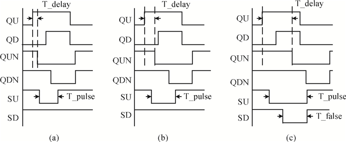
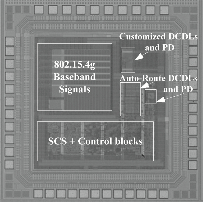
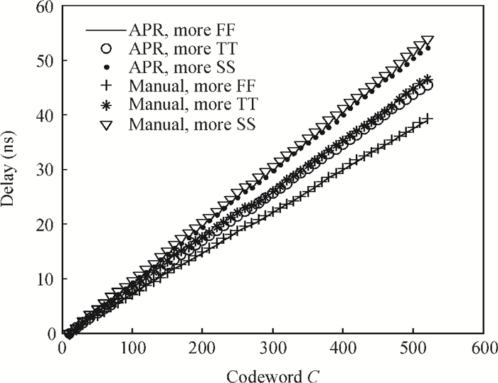
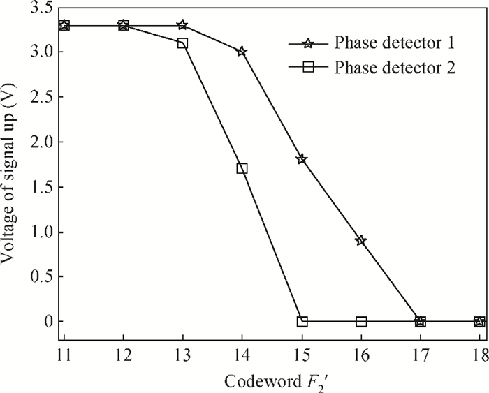
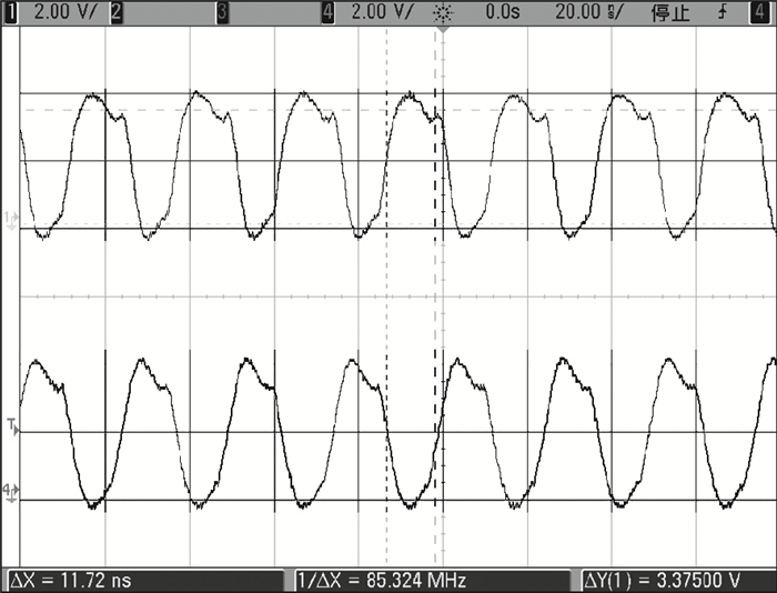
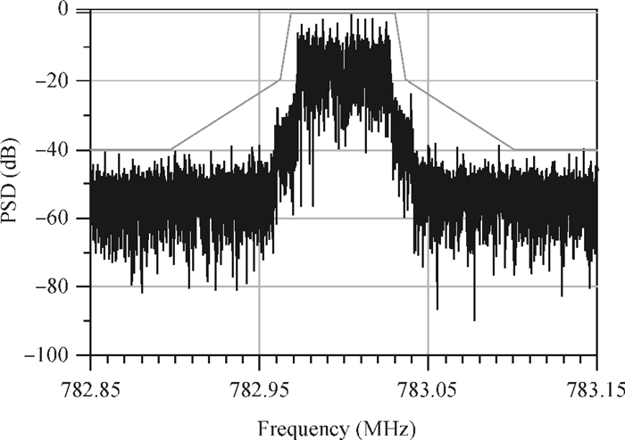
The linear amplification with nonlinear component transmitter is a promising solution to high efficiency and high linearity amplification for non-constant envelope signals. An all-digital synthesizable baseband for a delay-based LINC transmitter is implemented. This paper proposes a standard-cell based synthesizable methodology which can be applied in the ASIC process efficiently without performance degradation compared to the manual layout. A scheme to overcome the limited resolution of conventional phase detectors is proposed. It employs alternative phase detector structures to provide reconfigurability for higher resolution after fabricating, resulting in an 11 ps resolution improvement. Due to the PVT variation, an adaptive calibration scheme focusing on the inherent imbalance between two delay lines is depicted, which reveals an effective EVM enhancement of 5.37 dB. This baseband chip is implemented in 0.13 μm CMOS technology, and the transmitter with the baseband has an EVM of -28.96 dB and an ACPR of -29.51 dB, meeting the design requirement.


J. Semicond.
2014, 35(11): 115002 doi: 10.1088/1674-4926/35/11/115002

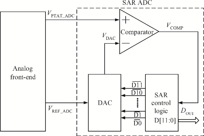
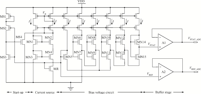
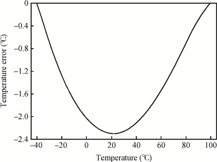
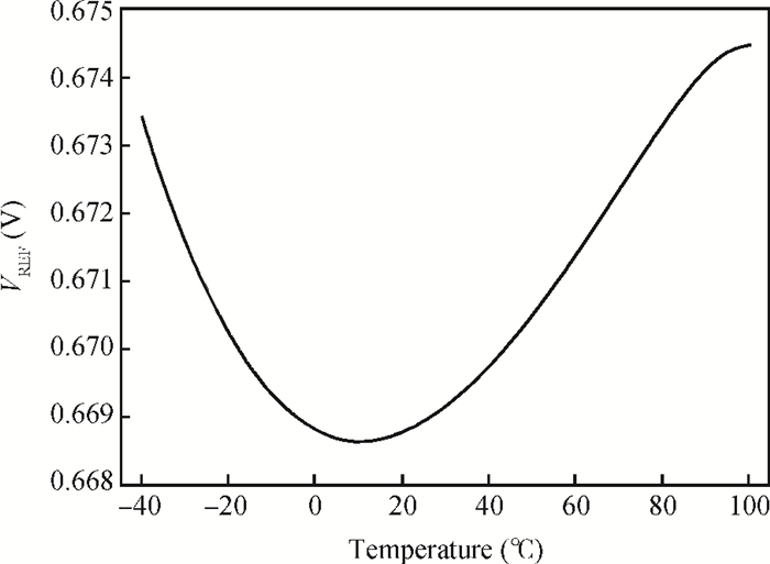
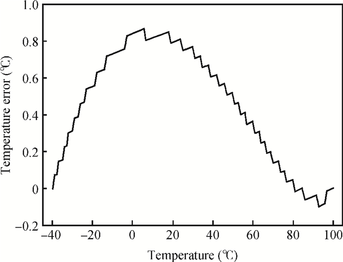
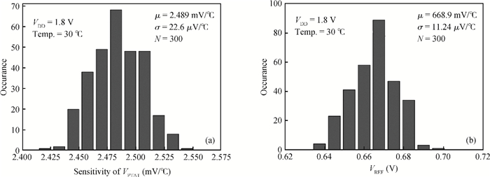
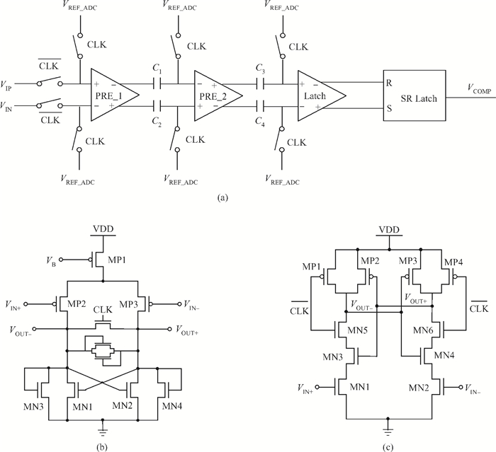
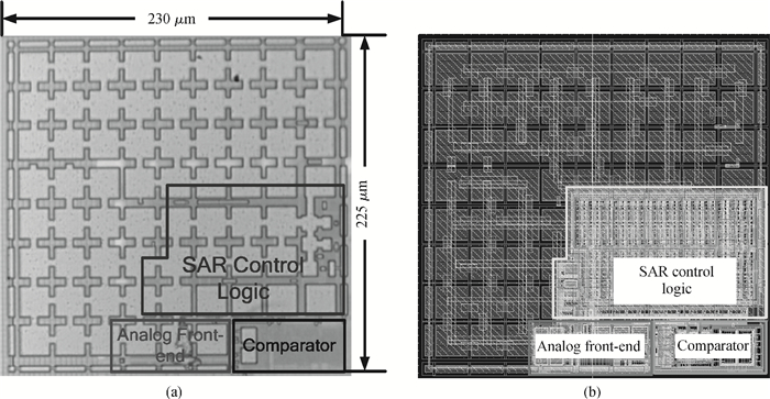
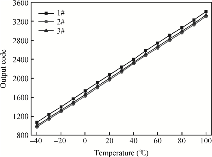
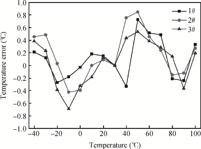
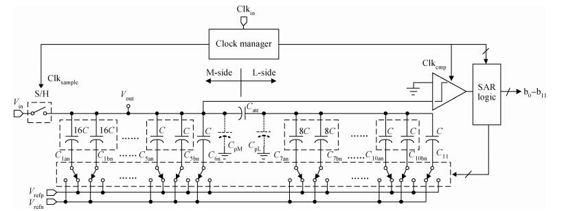
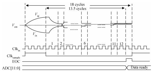
This paper presents the design and implement of a CMOS smart temperature sensor, which consists of a low power analog front-end and a 12-bit low-power successive approximation register (SAR) analog-to-digital converter (ADC). The analog front-end generates a proportional-to-absolute-temperature (PTAT) voltage with MOSFET circuits operating in the sub-threshold region. A reference voltage is also generated and optimized in order to minimize the temperature error and the 12-bit SAR ADC is used to digitize the PTAT voltage. Using 0.18 μm CMOS technology, measurement results show that the temperature error is -0.69/+0.85℃ after one-point calibration over a temperature range of -40 to 100℃. Under a conversion speed of 1K samples/s, the power consumption is only 2.02 μW while the chip area is 230×225 μm2, and it is suitable for RFID application.


J. Semicond.
2014, 35(11): 115003 doi: 10.1088/1674-4926/35/11/115003
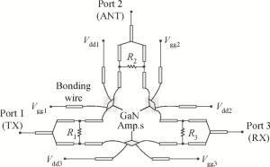
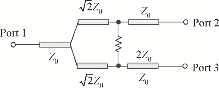
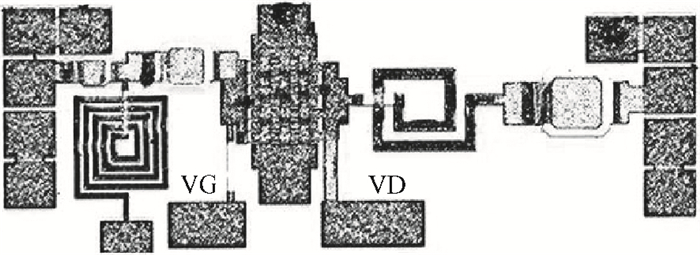
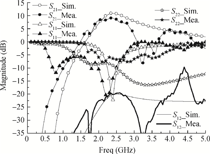
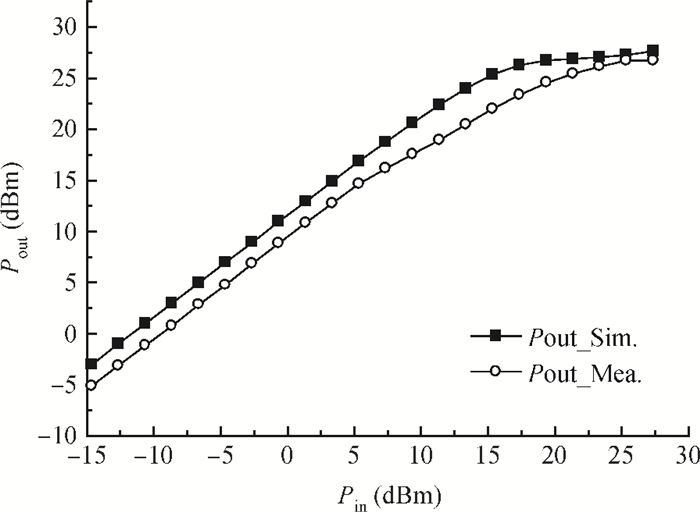
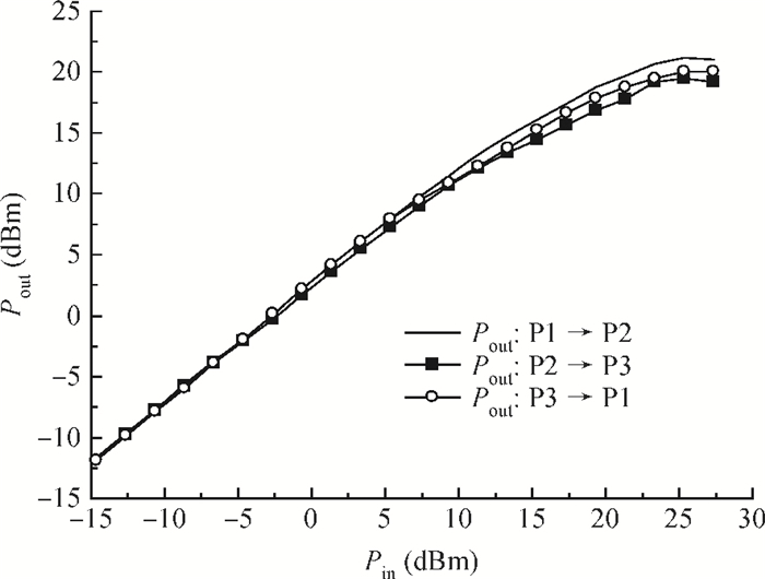
This paper presents a 2.4 GHz hybrid integrated active circulator consisting of three power amplifiers and three PCB-based Wilkinson power dividers. The power amplifiers were designed and fabricated in a standard 0.35-μm AlGaN/GaN HEMT technology, and combined with three traditional power dividers on FR4 using bonding wires. Due to the isolation of power dividers, the isolation between three ports is achieved; meanwhile, due to the unidirectional characteristics of the power amplifiers, the nonreciprocal transfer characteristic of the circulator is realized. The measured insertion gain of the proposed active circulator is about 2-2.7 dB at the center frequency of 2.4 GHz, the isolation between three ports is better than 20 dB over 1.2-3.4 GHz, and the output power of the designed active circulator achieves up to 20.1-21.2 dBm at the center frequency.


J. Semicond.
2014, 35(11): 115004 doi: 10.1088/1674-4926/35/11/115004
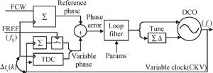
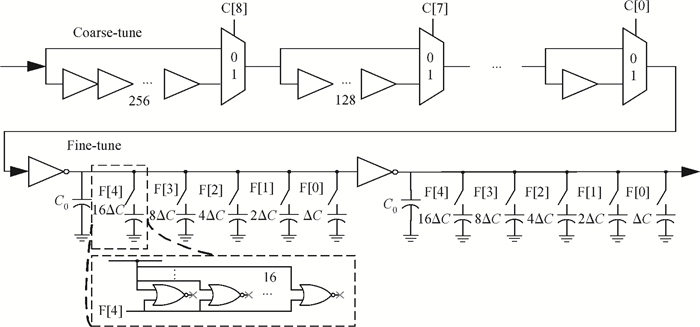
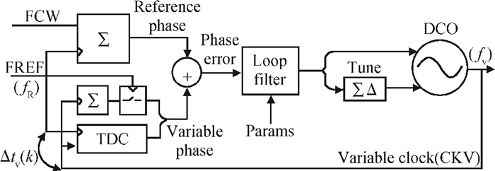
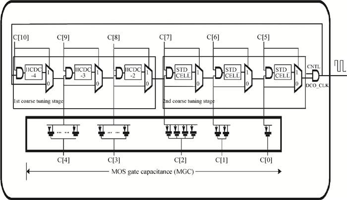
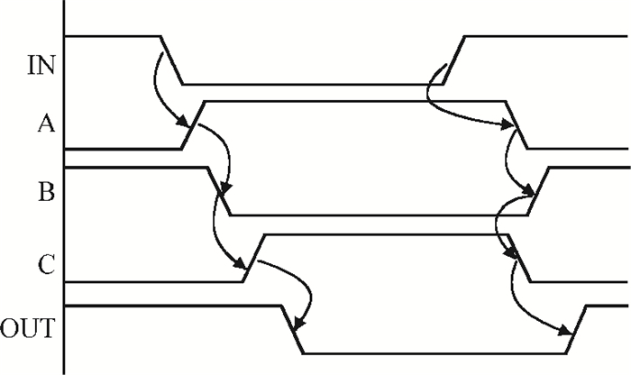
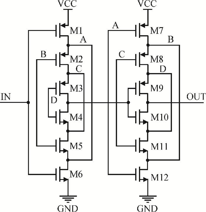
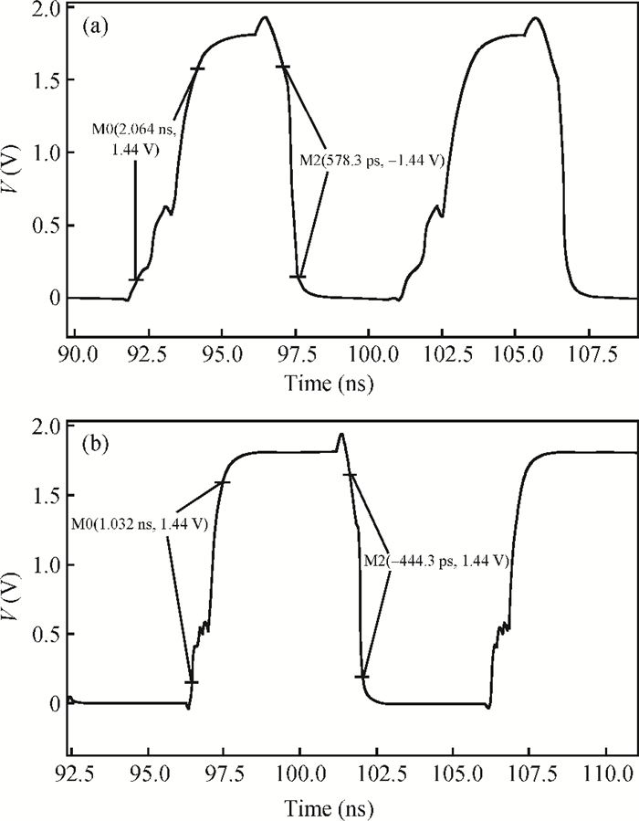
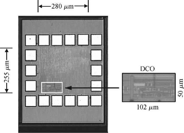
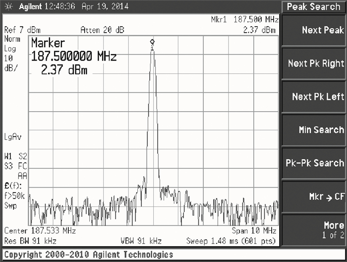
This paper presents a low-power small-area digitally controlled oscillator (DCO) using an inverters interlaced cascaded delay cell (IICDC). It uses a coarse-fine architecture with binary-weighted delay stages for the delay range and resolution. The coarse-tuning stage of the DCO uses IICDC, which is power and area efficient with low phase noise, as compared with conventional delay cells. The ADPLL with a DCO is fabricated in the UMC 180-nm CMOS process with an active area of 0.071 mm2. The output frequency range is 140-600 MHz at the power supply of 1.8 V. The power consumption is 2.34 mW@a 200 MHz output.


J. Semicond.
2014, 35(11): 115005 doi: 10.1088/1674-4926/35/11/115005
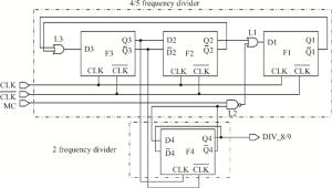
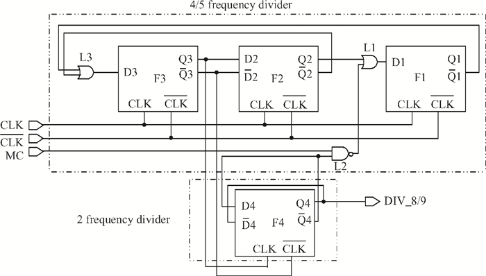
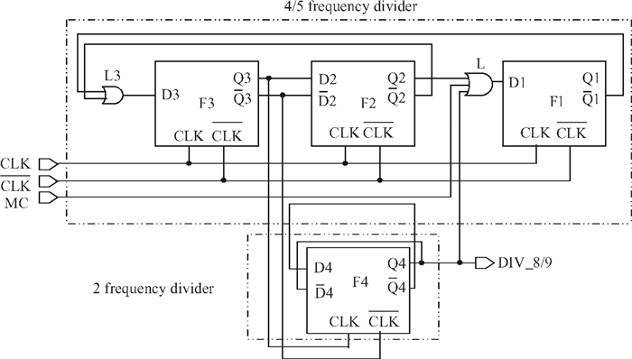
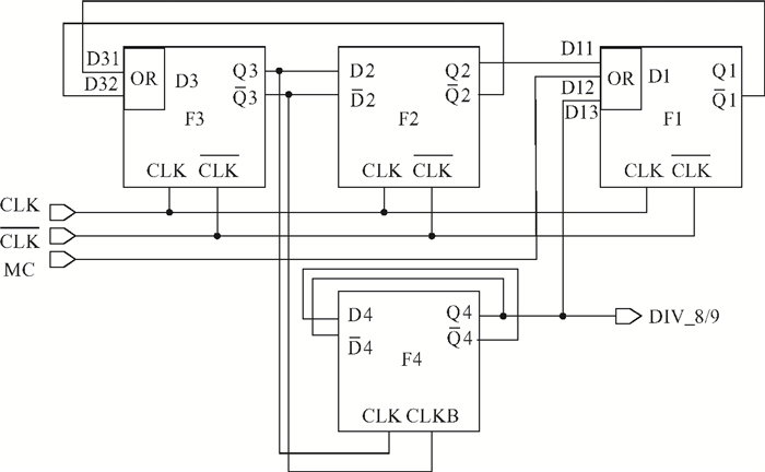
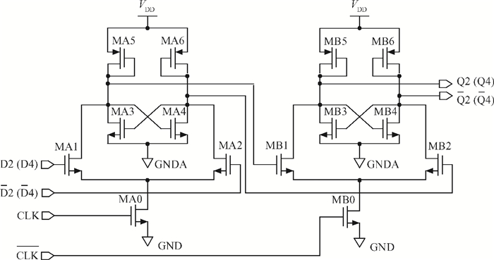
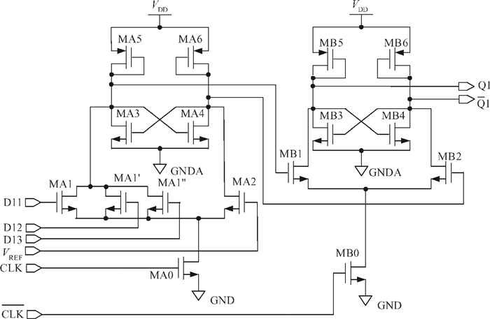
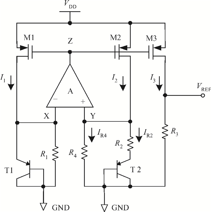
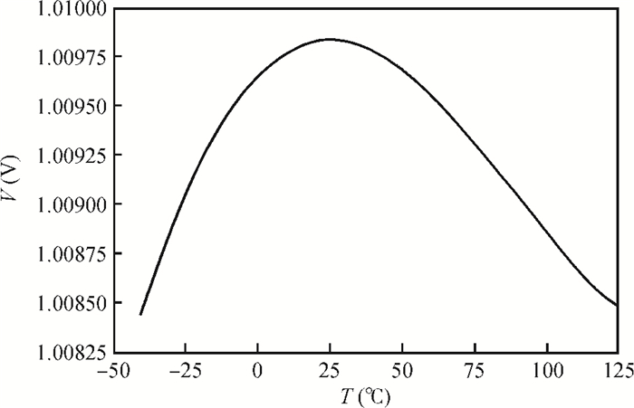
A fully integrated 2n/2n+1 dual-modulus divider in GHz frequency range is presented. The improved structure can make all separated logic gates embed into correlative D flip-flops completely. In this way, the complex logic functions can be performed with a minimum number of devices and with maximum speed, so that lower power consumption and faster speed are obtained. In addition, the low-voltage bandgap reference needed by the frequency divider is specifically designed to provide a 1.0 V output. According to the design demand, the circuit is fabricated in 0.18 μm standard CMOS process, and the measured results show that its operating frequency range is 1.1-2.5 GHz. The dual-modulus divider dissipates 1.1 mA from a 1.8 V power supply. The temperature coefficient of the reference voltage circuit is 8.3 ppm/℃ when the temperature varies from -40 to +125℃. By comparison, the dual-modulus divide designed in this paper can possess better performance and flexibility.


J. Semicond.
2014, 35(11): 115006 doi: 10.1088/1674-4926/35/11/115006
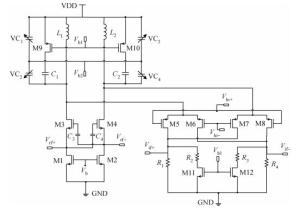
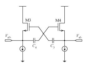
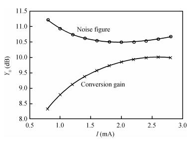
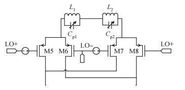
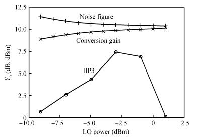
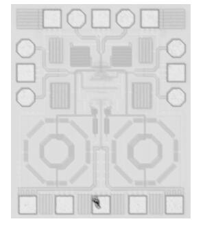
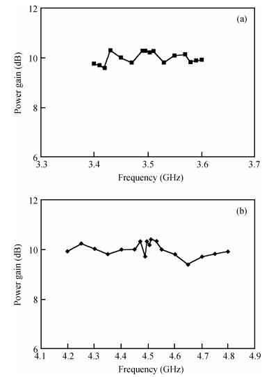
The design and analysis of a reconfigurable dual-band down-conversion mixer for IMT-advanced (3.4-3.6 GHz) and UWB (4.2-4.8 GHz) applications are presented. Based on a folded double-balanced Gilbert cell, which is well known for its low voltage, simplicity and well balanced performance, the mixer adopts a capacitive cross-coupling technique for input matching and performance improvement. Switched capacitors and resistors are added to shift the working bands. Fabricated in a TSMC 0.13 μm process, the test results show flat conversion gains from 9.6 to 10.3 dB on the IMT-A band and from 9.7 to 10.4 dB on the UWB band, with a noise figure of about 15 dB on both bands. The input third-order intercept points (ⅡP3) are about 7.3 dBm on both of the frequency bands. The whole chip consumes 11 mW under 1.2 V supply and the total area of the layout is 0.76×0.65 mm2.

J. Semicond.
2014, 35(11): 115007 doi: 10.1088/1674-4926/35/11/115007
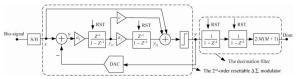
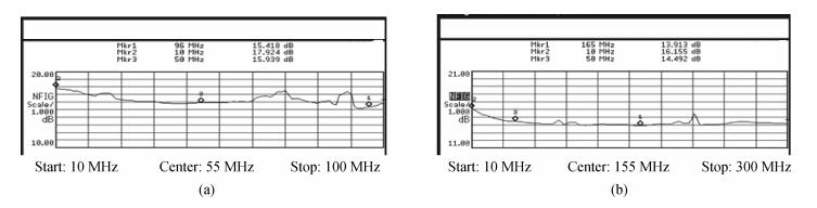
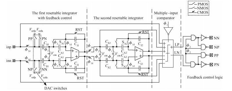
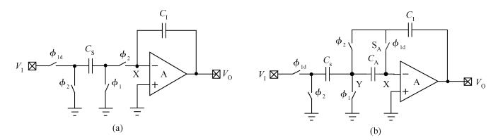
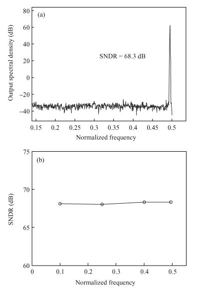
This paper presents an ultra-low power incremental ADC for biosensor interface circuits. The ADC consists of a resettable second-order delta-sigma (Δ Σ) modulator core and a resettable decimation filter. Several techniques are adopted to minimize its power consumption. A feedforward path is introduced to the modulator core to relax the signal swing and linearity requirement of the integrators. A correlated-double-sampling (CDS) technique is applied to reject the offset and 1/f noise, thereby removing the integrator leakage and relaxing the gain requirement of the OTA. A simple double-tailed inverter-based fully differential OTA using a thick-oxide CMOS is proposed to operate in the subthreshold region to fulfill both an ultra-low power and a large output swing at 1.2 V supply. The signal addition before the comparator in the feedforward architecture is performed in the current domain instead of the voltage domain to minimize the capacitive load to the integrators. The capacitors used in this design are of customized metal-oxide-metal (MOM) type to reach the minimum capacitance set by the kT/C noise limit. Fabricated with a 1P6M 0.18 μm CMOS technology, the presented incremental ADC consumes 600 nW at 2 kS/s from a 1.2 V supply, and achieves 68.3 dB signal to noise and distortion ratio (SNDR) at the Nyquist frequency and an FOM of 0.14 pJ/conversion step. The core area is 100×120 μm2.


J. Semicond.
2014, 35(11): 115008 doi: 10.1088/1674-4926/35/11/115008
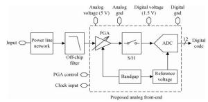
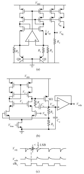
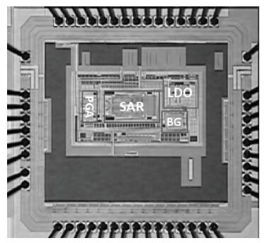
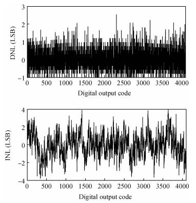
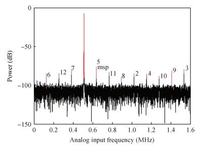
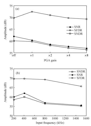
This paper presents an analog front end for a power line communication system, including a 12-bit 3.2-MS/s energy-efficient successive approximation register analog-to-digital converter, a positive feedback programmable gain amplifier, a 9.8 ppm/℃ bandgap reference and on-chip low-output voltage regulators. A two segment capacitive array structure (6 MSB 5 LSB) composed by split capacitors is designed for the SAR core to save area cost and release reference voltage accuracy requirements. Implemented in the GSMC 0.13 μm 1.5 V/12 V dual-gate 4P6M e-flash process, the analog front end occupies an area of 0.457 mm2 and consumes power of 18.8 mW, in which 1.1 mW cost by the SAR ADC. Measured at 500 kHz input, the spurious-free dynamic range and signal-to-noise plus distortion ratio of the ADC are 71.57 dB and 60.60 dB respectively, achieving a figure of merit of 350 fJ/conversion-step.

J. Semicond.
2014, 35(11): 115009 doi: 10.1088/1674-4926/35/11/115009
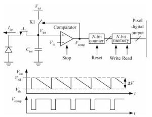
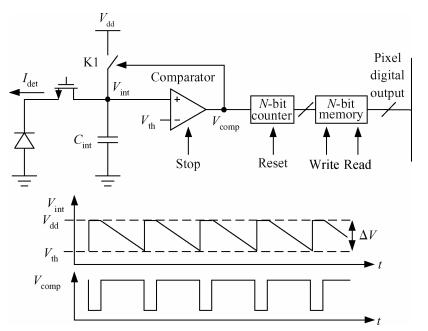
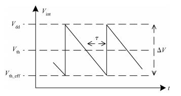
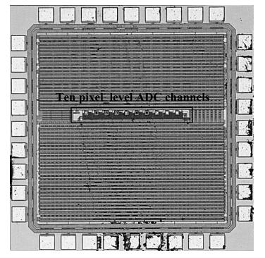
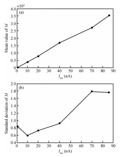
This paper presents a 50 Hz 15-bit analog-to-digital converter (ADC) for pixel-level implementation in CMOS image sensors. The ADC is based on charge packets counting and adopts a voltage reset technique to inject charge packets. The core circuit for charge/pulse conversion is specially optimized for low power, low noise and small area. An experimental chip with ten pixel-level ADCs has been fabricated and tested for verification. The measurement result shows a standard deviation of 1.8 LSB for full-scale output. The ADC has an area of 45×45 μm2 and consumes less than 2 μW in a standard 1P-6M 0.18 μm CMOS process.

J. Semicond.
2014, 35(11): 115010 doi: 10.1088/1674-4926/35/11/115010
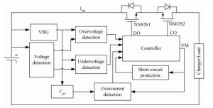
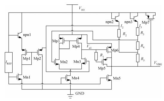
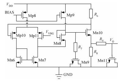
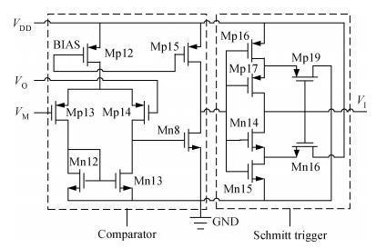
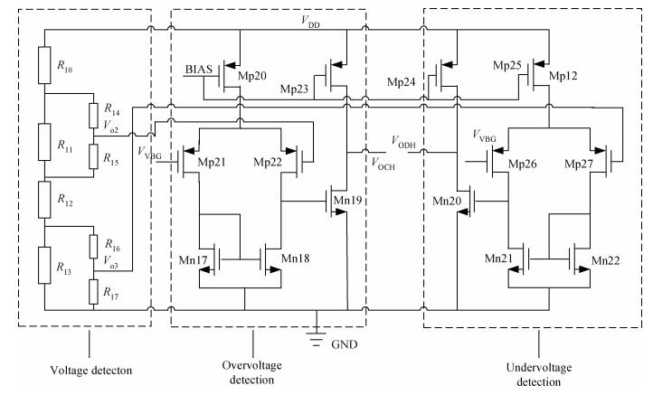
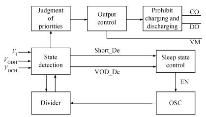
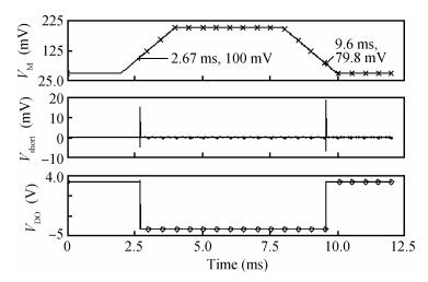
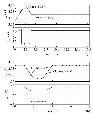
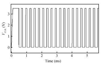
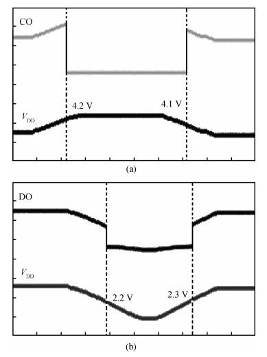
A single lithium-ion battery protection circuit with high reliability and low power consumption is proposed. The protection circuit has high reliability because the voltage and current of the battery are controlled in a safe range. The protection circuit can immediately activate a protective function when the voltage and current of the battery are beyond the safe range. In order to reduce the circuit's power consumption, a sleep state control circuit is developed. Additionally, the output frequency of the ring oscillation can be adjusted continuously and precisely by the charging capacitors and the constant-current source. The proposed protection circuit is fabricated in a 0.5 μm mixed-signal CMOS process. The measured reference voltage is 1.19 V, the overvoltage is 4.2 V and the undervoltage is 2.2 V. The total power is about 9 μW.


J. Semicond.
2014, 35(11): 115011 doi: 10.1088/1674-4926/35/11/115011
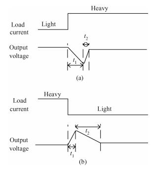
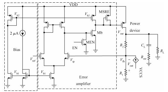
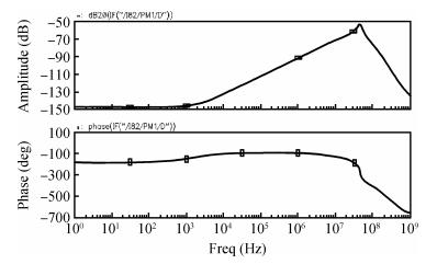
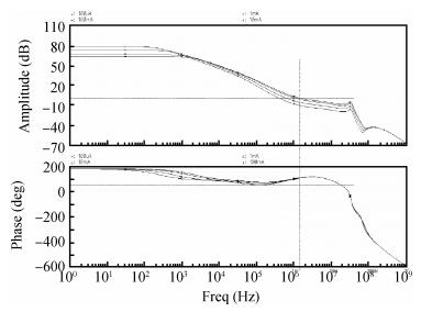
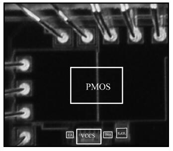
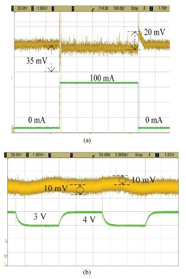
A stable LDO using VCCS (voltage control current source) is presented. The LDO is designed and implemented on GF 2P4M 0.35 μm CMOS technology. Compared with a previous compensation scheme, VCCS can implement a real stable LDO with a small on-chip capacitor of 1 pF, whose stability is not affected by the variable ESR (equivalent series resistance) of the output capacitor. The unit gain frequency of the LDO loop can achieve 1.5 MHz, improving the transient response. The PSR of the LDO is larger than 45 dB within 0-40 kHz. The static current of the LDO at heavy load of 100 mA is 57 μA and the dropout voltage of the LDO is 150 mV. Experimental results show that a setting time of 10 μs is achieved, and the variation of output voltage is smaller than 35 mV for a 100 mA load step in transient response of the LDO.


J. Semicond.
2014, 35(11): 116001 doi: 10.1088/1674-4926/35/11/116001
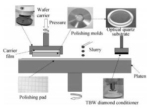
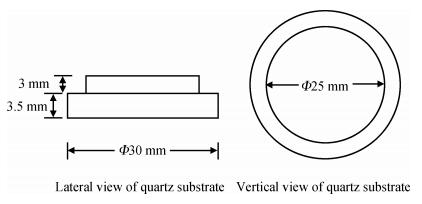
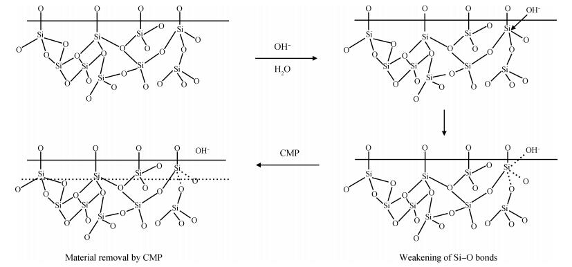
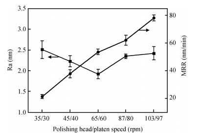
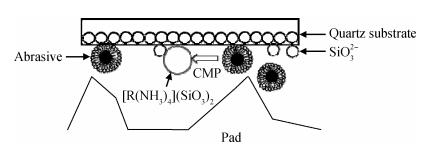
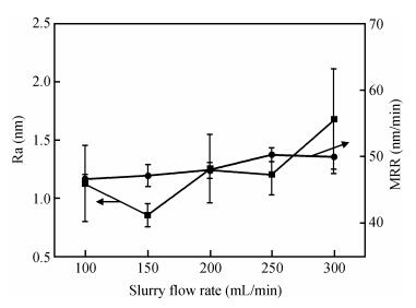
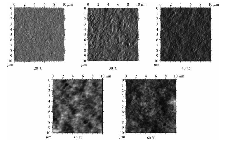
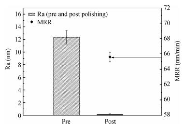
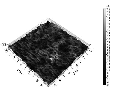
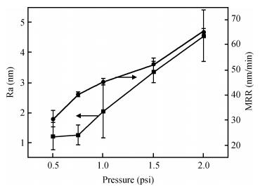
In order to achieve a high-quality quartz glass substrate and to improve the performance of TiO2 anti-reflection coating, chemical mechanical polishing (CMP) method was used. During CMP process, some process parameters including pressure, polishing head speed, platen speed, slurry flow rate, polishing time, and slurry temperature were optimized to obtain lower quartz surface roughness. According to the experiment results, when pressure was 0.75 psi, polishing head speed was 65 rpm, platen speed was 60 rpm, slurry flow rate 150 mL/min, slurry temperature 20℃, and polishing time was 60 s, the material removal rate (MRR) was 56.8 nm/min and the surface roughness (Ra) was 1.93 Å (the scanned area was 10×10 μm2). These results were suitable for the industrial production requirements.


J. Semicond.
2014, 35(11): 116002 doi: 10.1088/1674-4926/35/11/116002
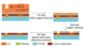
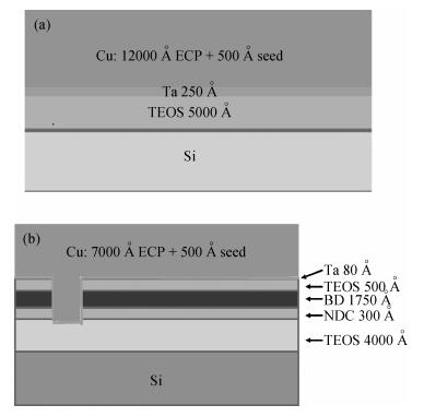
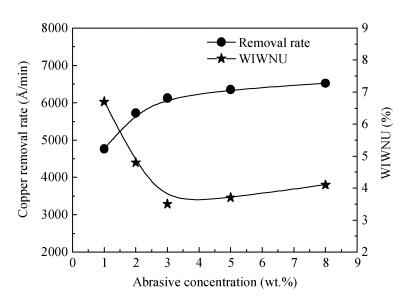
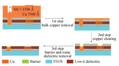
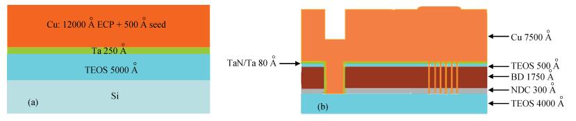
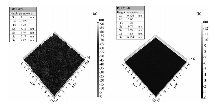
A novel alkaline copper slurry that possesses a relatively high planarization performance is investigated under a low abrasive concentration. Based on the action mechanism of CMP, the feasibility of using one type of slurry in copper bulk elimination process and residual copper elimination process, with different process parameters, was analyzed. In addition, we investigated the regular change of abrasive concentration effect on copper and tantalum removal rate and within wafer non-uniformity (WIWNU) in CMP process. When the abrasive concentration is 3 wt%, in bulk elimination process, the copper removal rate achieves 6125 Å/min, while WIWNU is 3.5%, simultaneously. In residual copper elimination process, the copper removal rate is approximately 2700 Å/min, while WIWNU is 2.8%. Nevertheless, the tantalum removal rate is 0 Å/min, which indicates that barrier layer isn't eliminated in residual copper elimination process. The planarization experimental results show that an excellent planarization performance is obtained with a relatively high copper removal rate in bulk elimination process. Meanwhile, after residual copper elimination process, the dishing value increased inconspicuously, in a controllable range, and the wafer surface roughness is only 0.326 nm (sq < 1 nm) after polishing. By comparison, the planarization performance and surface quality of alkaline slurry show almost no major differences with two kinds of commercial acid slurries after polishing. All experimental results are conducive to research and improvement of alkaline slurry in the future.

J. Semicond.
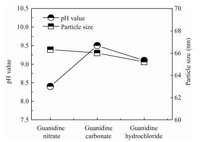
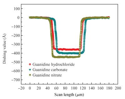
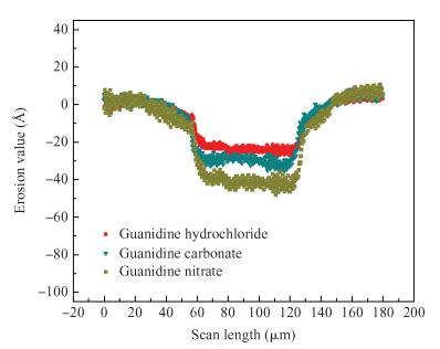
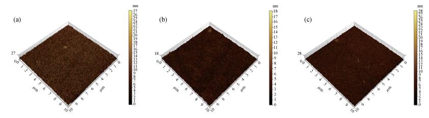
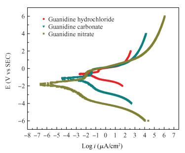
2014, 35(11): 116003 doi: 10.1088/1674-4926/35/11/116003
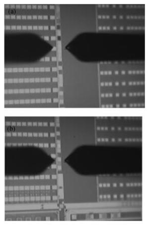
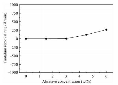
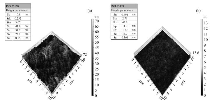
The influence of three kinds of guanidinium salt on the removal rate selectivity of different materials was studied during the barrier chemical mechanical polishing (CMP) process at first. The three kinds of guanidine saltguanidine hydrochloride, guanidine nitrate and guanidine carbonate. Then we compared the effect of the three kinds of guanidine salt on the dishing, erosion and surface roughness value. In the end, the reaction mechanism was studied through electrochemical analysis. All the results indicate that there is a better performance of the slurry with guanidine hydrochloride than the slurries with the other two kinds of guanidine salt. It effectively improved the removal rate selectivity and the surface roughness under the premise of low abrasive concentration and low polishing pressure, which is good for the optimization of the alkaline slurry for the barrier CMP process.


J. Semicond.
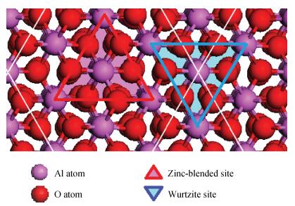
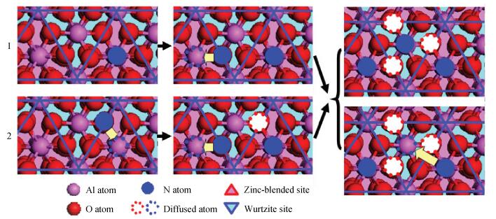
2014, 35(11): 116004 doi: 10.1088/1674-4926/35/11/116004

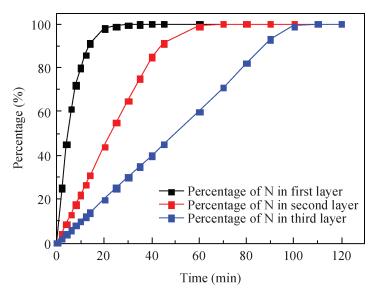
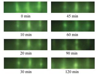
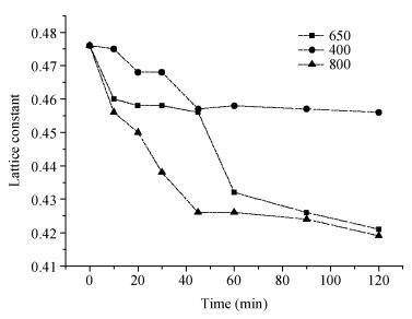
We established a model to simulate the growth process of nitridation and clarified the inner mechanisms of nitridation and over-nitridation by combining the kinetic Monte Carlo and molecular dynamics methods. Supported by reflection high-energy electron diffraction results with growth in an MBE system, the tendency of nitridation on α -sapphire in different conditions was observed and analyzed. The best conditions for nitridation on the α -sapphire surface are found by our simulation.

J. Semicond.
2014, 35(11): 116005 doi: 10.1088/1674-4926/35/11/116005

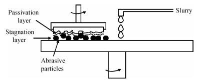
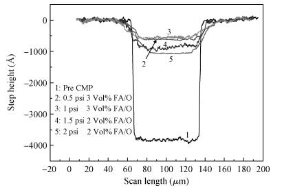
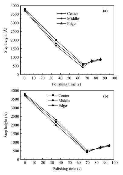
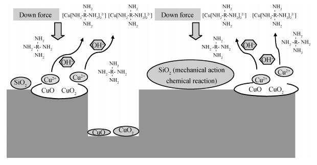
We propose the action mechanism of Cu chemical mechanical planarization (CMP) in an alkaline solution. Meanwhile, the effect of abrasive mass fraction on the copper removal rate and within wafer non-uniformity (WIWNU) have been researched. In addition, we have also investigated the synergistic effect between the applied pressure and the FA/O chelating agent on the copper removal rate and WIWNU in the CMP process. Based on the experimental results, we chose several concentrations of the FA/O chelating agent, which added in the slurry can obtain a relatively high removal rate and a low WIWNU after polishing, to investigate the planarization performance of the copper slurry under different applied pressure conditions. The results demonstrate that the copper removal rate can reach 6125 Å/min when the abrasive concentration is 3 wt.%. From the planarization experimental results, we can see that the residual step height is 562 Å after excessive copper of the wafer surface is eliminated. It denotes that a good polishing result is acquired when the FA/O chelating agent concentration and applied pressure are fixed at 3 vol% and 1 psi, respectively. All the results set forth here are very valuable for the research and development of alkaline slurry.