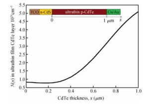
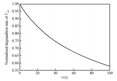
The defect distribution across an ultrathin film CdTe layer of a CdS/CdTe solar cell is modelled by solving the balance equation in steady state. The degradation of the device parameters, because of the defect induced through ion implantation, was considered. The degradation is accelerated if the ion implanted defect distribution is considerable. The defect concentration is maximum at the surface of the CdTe layer where implantation is applied and it is minimum at the junction with the CdS layer (CdS/CdTe). The ultrathin device is under exposure of a fast degradation if the defect concentration is high at the junction. Since the front and back contacts of the device are close and the electric field is strong to drive the defects into the junction, the p-doping process might be precisely controlled. The modeling results presented here are in agreement with the few available experimental reports in the literature on the degradation and defect configuration of the ultrathin CdTe films.

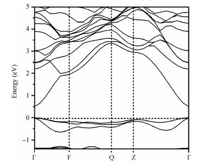
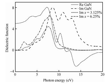
The electronic and optical properties of the ternary GaN1-xBix alloys in the zinc-blende structure are theoretically investigated by first principles calculations. Geometric optimization is performed before all the simulations to get accurate results. The band gaps of the alloys are found to be direct even with x=6.25%, and would become smaller when increasing the Bi compositions. The decrease ratio of band gaps is approximately 227 meV when 1% of N is replaced by Bi in the range of x=0-6.25%. Meanwhile, the absorption coefficient is shown to be significantly changed induced by the incorporation of Bi. These interesting properties indicate that GaN1-xBix alloys could be a promising candidate in future optoelectronic applications.


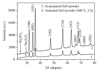
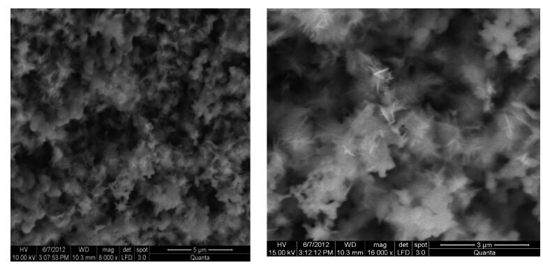
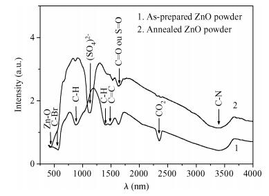
Zinc oxide nanoscale powder has been synthesized by a hydrothermal route using zinc sulfate and sodium hydroxide. The as-prepared powder was annealed at 600℃ for 2 h and then characterized by X-ray diffraction (XRD), scanning electron microscopy and infra-red Fourier transformed spectroscopy. XRD measurements have shown a ZnO hexagonal wurtzite polycrystalline structure with good crystallinity and the formation of a new sodium pyrosulfate phase in the as-prepared powder. The annealing improves the crystalline quality of the powder and transforms the sodium pyrosulfate phase to a sodium sulfate one. The thermal treatment does not affect the lattice parameters and the Zn-O bond length but improves the random orientation of the ZnO crystallites growth. ZnO crystallites have an interconnected-nano-needles morphology forming irregular shaped aggregates. The size of the crystallites is about 20 nm. EDX analysis has shown the presence of C and S in addition to Zn and O. FTIR spectra confirm the formation of ZnO and sodium sulfate. The synthesized ZnO powder has a very high crystalline quality and the used method is a very advantageous one for the fabrication of nanosized metal oxides from inorganic reactants for photo-catalysis applications.

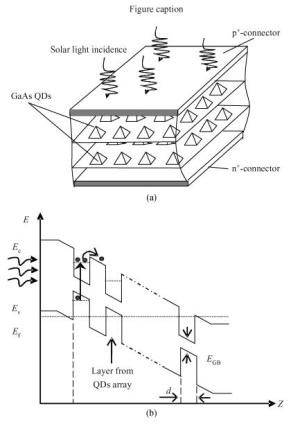
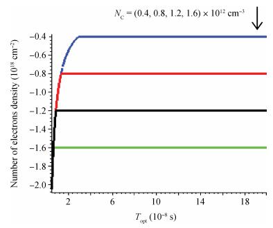
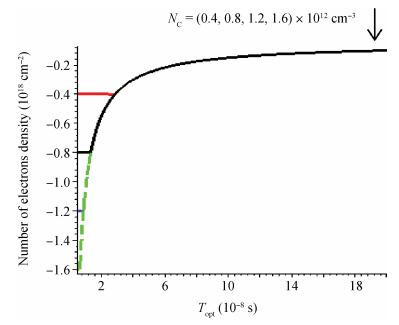
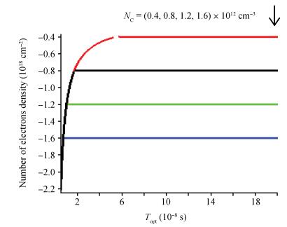
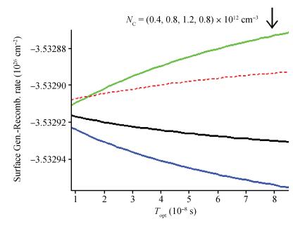
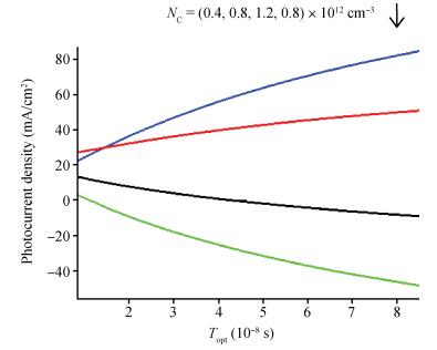
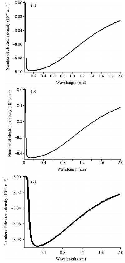
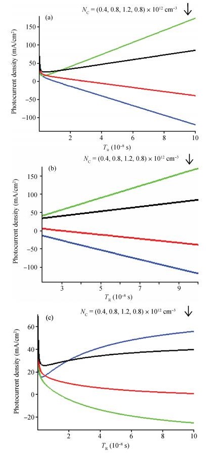
The main goal of this paper is to determine the accurate values of two parameters namely the surface generation-recombination rate and the average total number of electrons density generated in the i-region. These values will enhance the performance of quantum dot solar cells (QDSCs). In order to determine these values, this paper concentrates on the optical generation lifetime, the recombination lifetime, and the effective density state in QDs. Furthermore, these parameters are studied in relation with the average total number of electrons density. The values of the surface generation-recombination rate are found to be negative, which implies that the generation process is dominant in the absorption quantum dot region. Consequently, induced photocurrent density relation with device parameters is determined. The results ensure that QDSCs can have higher response photocurrent and then improve the power conversion efficiency. Moreover, the peak value of the average total number of electrons density is achieved at the UV range and is extended to the visible range, which is adequate for space and ground solar applications.


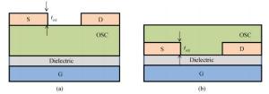
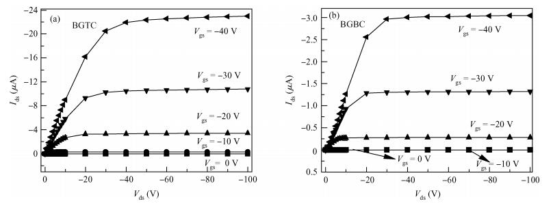
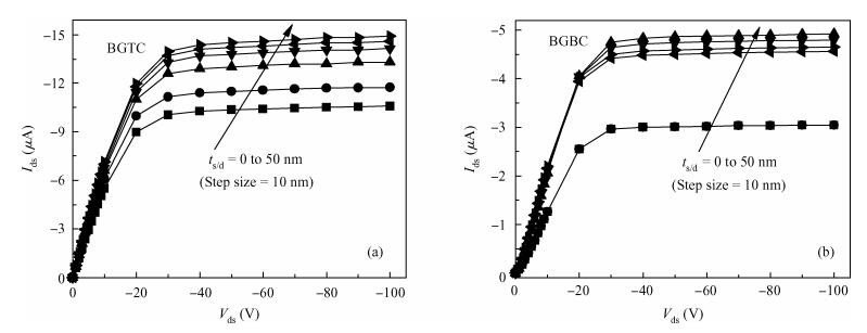
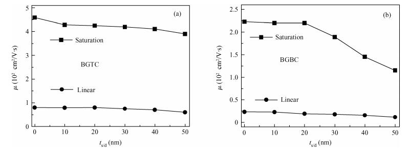
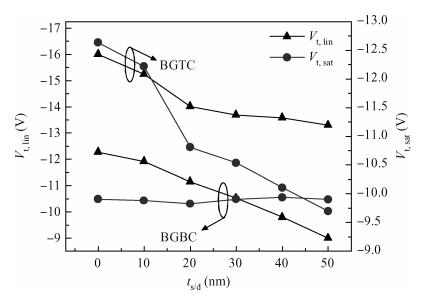
This paper analyzes the impact of source (ts) and drain (td) contact thicknesses on top contact (TC) and bottom contact (BC) organic thin film transistors (OTFTs) with a gate in the bottom, using a benchmarked industry standard Atlas 2-D numerical device simulator. The parameters including drive current (Ids), mobility (μ), threshold voltage (Vt) and current on-off ratio (ION/IOFF) are analyzed from the device physics point of view on different electrode thicknesses, ranging from infinitesimal to 50 nm, for both top and bottom contact structures. Observations demonstrate that the performance of the BC structure is more affected by scaling of ts/d in comparison to its counterpart. In the linear region, the mobility is almost constant at all the values of ts/d for both structures. However, an increment of 18% and 83% in saturation region mobility is found for TC and BC structures, respectively with scaling down ts/d from 50-0 nm. Besides this, the current on-off ratio increases more sharply in the BC structure. This analysis simplifies a number of issues related to the design and fabrication of organic material based devices and circuits.


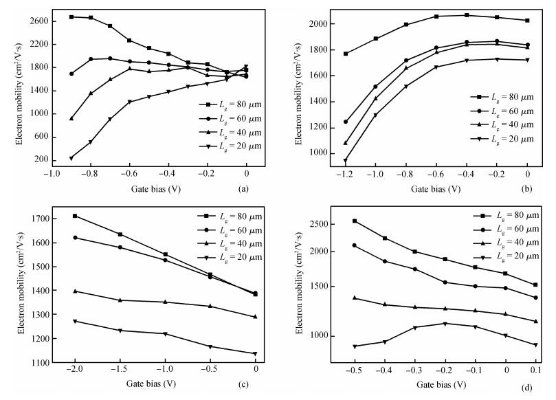
Using the measured capacitance-voltage and current-voltage characteristics of the rectangular AlN/GaN heterostructure field-effect transistors (HFETs) with the side-Ohmic contacts, it was found that the polarization Coulomb field scattering in the AlN/GaN HFETs was greatly weakened after the side-Ohmic contact processing, however, it still could not be ignored. It was also found that, with side-Ohmic contacts, the polarization Coulomb field scattering was much stronger in AlN/GaN HFETs than in AlGaN/AlN/GaN and In0.17Al0.83N/AlN/GaN HFETs, which was attributed to the extremely thinner barrier layer and the stronger polarization of the AlN/GaN heterostructure.
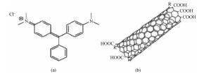
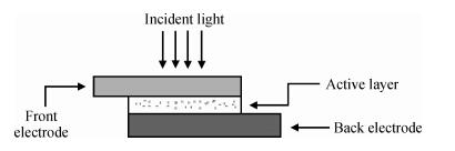
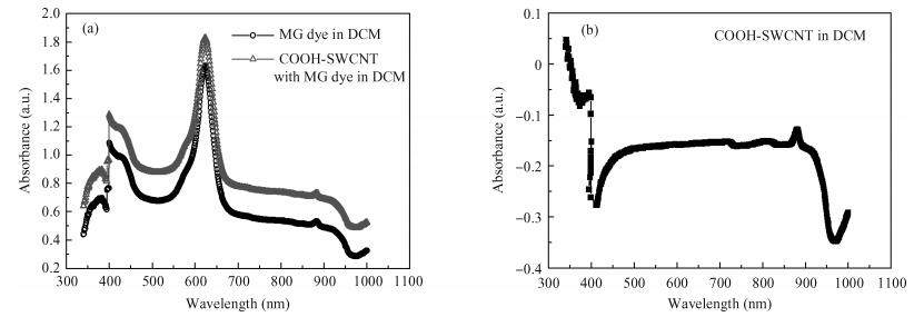
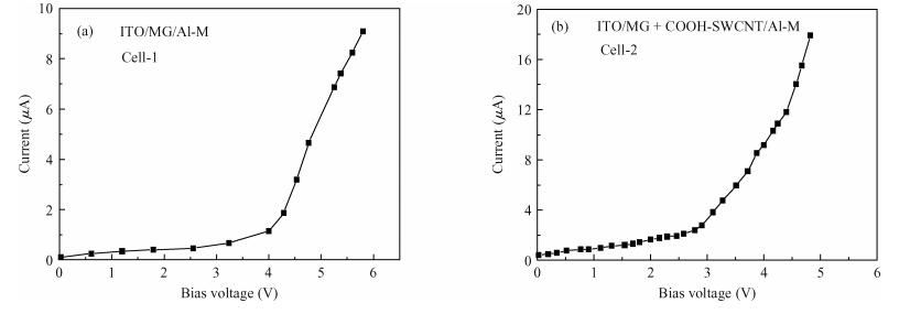
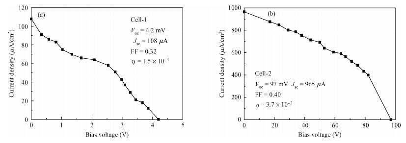
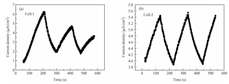
We report the effect of COOH-functionalized single walled carbon nanotubes (COOH-SWCNT) on the electrical and photovoltaic characteristics of Malachite Green (MG) dye based photovoltaic cells. Two different types of photovoltaic cells were prepared, one with MG dye and another by incorporating COOH-SWCNT with this dye. Cells were characterized through different electrical and photovoltaic measurements including photocurrent measurements with pulsed radiation. From the dark current-voltage (I-V) characteristic results, we observed a certain transition voltage (Vth) for both the cells beyond which the conduction mechanism of the cells change sharply. For the MG dye, Vth is 3.9 V whereas for COOH-SWCNT mixed with this dye, Vth drops to 2.7 V. The device performance improves due to the incorporation of COOH-SWCNT. The open circuit voltage (Voc) and short circuit current density change from 4.2 to 97 mV and from 108 to 965 μA/cm2 respectively. Observations from photocurrent measurements show that the rate of growth and decay of the photocurrent are quite faster in the presence of COOH-SWCNT. This observation indicates a faster charge separation processes due to the incorporation of COOH-SWCNT in the MG dye cells. The high aspect ratio of COOH-SWCNT allows efficient conduction pathways for the generated charge carriers.


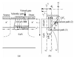
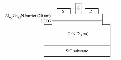
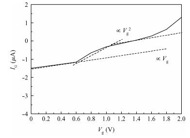
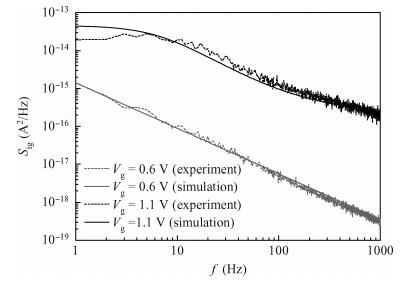
This work presents a theoretical and experimental study on the gate current 1/f noise in AlGaN/GaN HEMTs. Based on the carrier number fluctuation in the two-dimensional electron gas channel of AlGaN/GaN HEMTs, a gate current 1/f noise model containing a trap-assisted tunneling current and a space charge limited current is built. The simulation results are in good agreement with the experiment. Experiments show that, if Vg < Vx (critical gate voltage of dielectric relaxation), gate current 1/f noise comes from the superimposition of trap-assisted tunneling RTS (random telegraph noise), while Vg > Vx, gate current 1/f noise comes from not only the trap-assisted tunneling RTS, but also the space charge limited current RTS. This indicates that the gate current 1/f noise of the GaN-based HEMTs device is sensitive to the interaction of defects and the piezoelectric relaxation. It provides a useful characterization tool for deeper information about the defects and their evolution in AlGaN/GaN HEMTs.

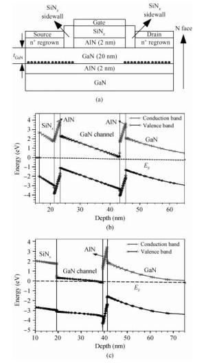
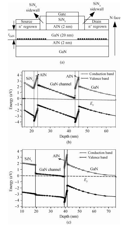
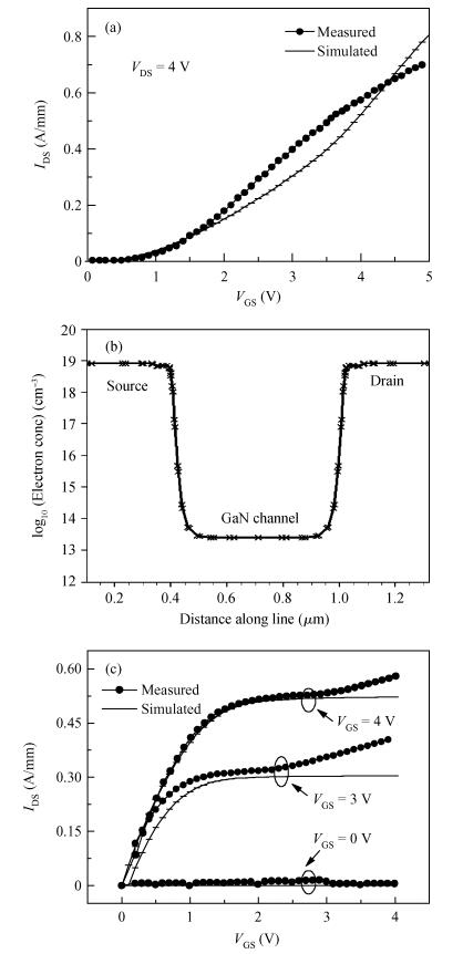
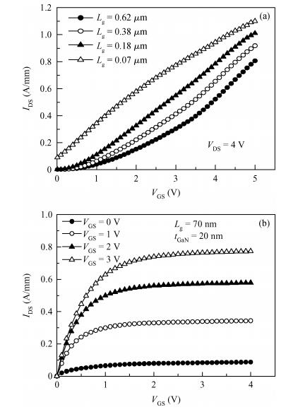
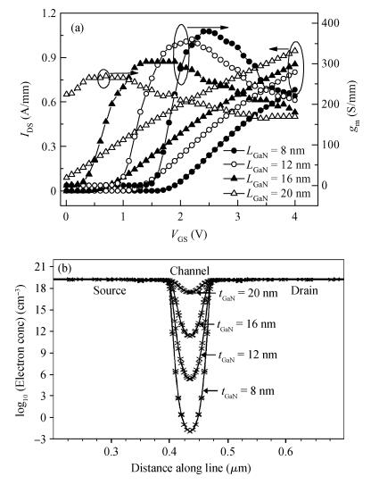
This paper aims to simulate the I-V static characteristic of the enhancement-mode (E-mode) N-polar GaN metal-insulator-semiconductor field effect transistor (MISFET) with self-aligned source/drain regions. Firstly, with SILVACO TCAD device simulation, the drain-source current as a function of the gate-source voltage is calculated and the dependence of the drain-source current on the drain-source voltage in the case of different gate-source voltages for the device with a 0.62 μm gate length is investigated. Secondly, a comparison is made with the experimental report. Lastly, the transfer characteristic with different gate lengths and different buffer layers has been performed. The results show that the simulation is in accord with the experiment at the gate length of 0.62 μm and the short channel effect becomes pronounced as gate length decreases. The E-mode will not be held below a 100 nm gate length unless both transversal scaling and vertical scaling are being carried out simultaneously.
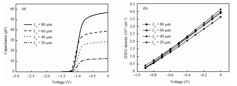
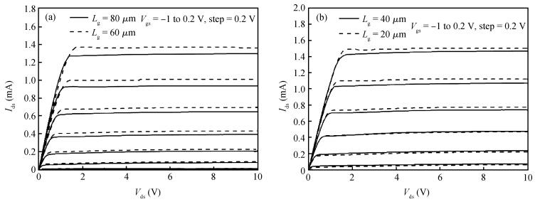
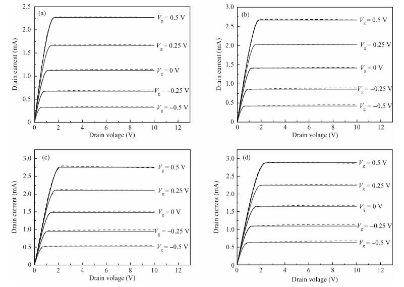
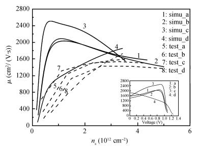
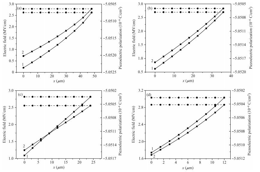
Based on the measured capacitance-voltage (C-V) curves and current-voltage (I-V) curves for the prepared differently-sized AlN/GaN heterostructure field-effect transistors (HFETs), the I-V characteristics of the AlN/GaN HFETs were simulated using the quasi-two-dimensional (quasi-2D) model. By analyzing the variation in the electron mobility for the two-dimensional electron gas (2DEG) with the channel electric field, it is found that the different polarization charge distribution generated by the different channel electric field distribution can result in different polarization Coulomb field (PCF) scattering. The 2DEG electron mobility difference is mostly caused by the PCF scattering which can reach up to 899.6 cm2/(V·s) (sample a), 1307.4 cm2/(V·s) (sample b), 1561.7 cm2/(V·s) (sample c) and 678.1 cm2/(V·s) (sample d), respectively. When the 2DEG sheet density is modulated by the drain-source bias, the electron mobility for samples a, b and c appear to peak with the variation of the 2DEG sheet density, but for sample d, no peak appears and the electron mobility rises with the increase in the 2DEG sheet density.

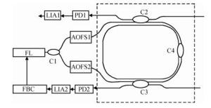
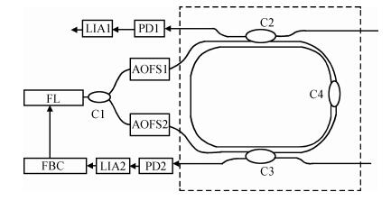
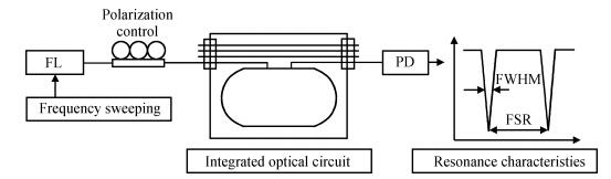
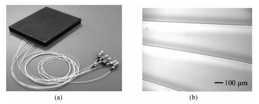
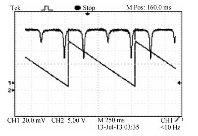
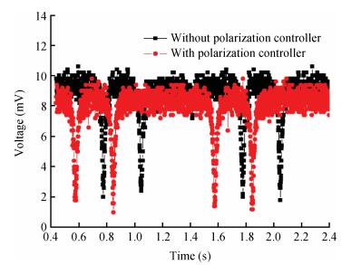
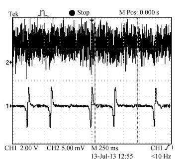
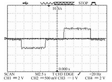
This paper reports the experimental results of silica on a silicon ring resonator in a resonator micro optic gyroscope based on the frequency modulation spectroscopy technique by our research group. The ring resonator is composed of a 4 cm diameter silica waveguide. By testing at λ=1550 nm, the FSR, FWHM and the depth of resonance are 3122 MHz, 103.07 MHz and 0.8 respectively. By using a polarization controller, the resonance curve under the TM mode can be inhibited. The depth of resonance increased from 0.8 to 0.8913, namely the finesse increase from 30.33 to 33.05. In the experiments, there is an acoustic-optical frequency shifter (AOFS) in each light loop. We lock the lasing frequency at the resonance frequency of the silica waveguide ring resonator for the counterclockwise lightwave; the frequency difference between the driving frequencies of the two AOFS is equivalent to the Sagnac frequency difference caused by gyro rotation. Thus, the gyro output is observed. The slope of the linear fit is about 0.330 mV/(°/s) based on the -900 to 900 kHz equivalent frequency and the gyro dynamic range is ±2.0×10³ rad/s.


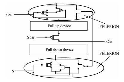
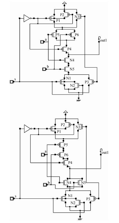
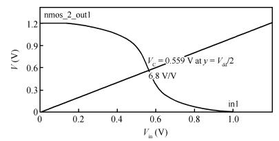
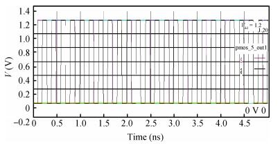
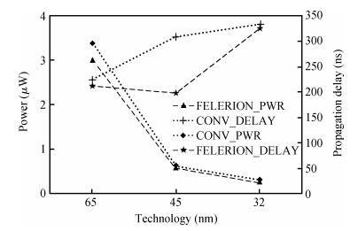
The circuit proposed in this paper simultaneously reduces the sub threshold leakage power and saves the state of art aspect of the logic circuits. Sleep transistors and PMOS-only logic are used to further reduce the leakage power. Sleep transistors are used as the keepers to reduce the sub threshold leakage current providing the low resistance path to the output. PMOS-only logic is used between the pull up and pull down devices to mitigate the leakage power further. Our proposed fast efficient leakage reduction circuit not only reduces the leakage current but also reduces the power dissipation. Power and delay are analyzed at the 32 nm BSIM4 model for a chain of four inverters, NAND, NOR and ISCAS-85 c17 benchmark circuits using DSCH3 and the Microwind tool. The simulation results reveal that our proposed approach mitigates leakage power by 90%-94% as compared to the conventional approach.

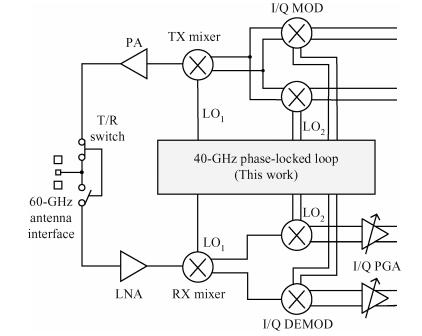
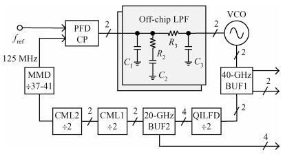
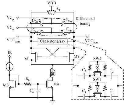
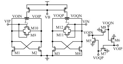
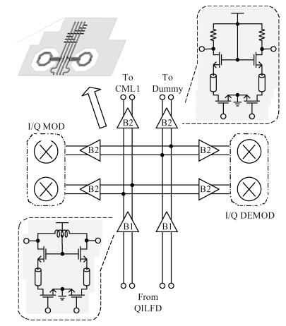
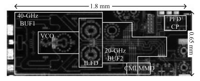
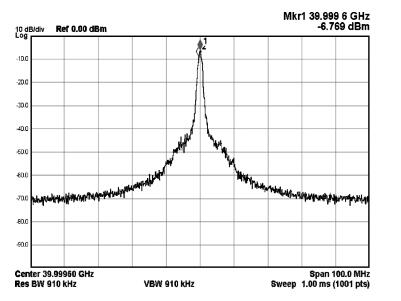
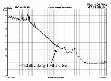
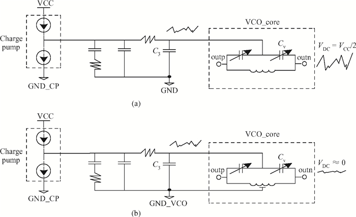
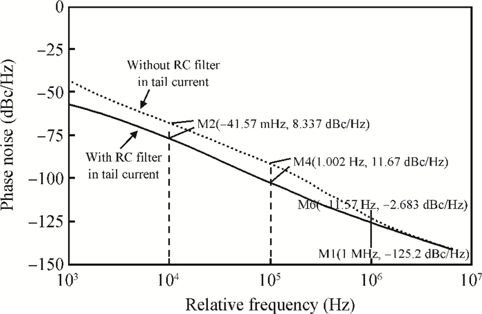
A 40-GHz phase-locked loop (PLL) frequency synthesizer for 60-GHz wireless communication applications is presented. The electrical characteristics of the passive components in the VCO and LO buffers are accurately extracted with an electromagnetic simulator HFSS. A differential tuning technique is utilized in the voltage controlled oscillator (VCO) to achieve higher common-mode noise rejection and better phase noise performance. The VCO and the divider chain are powered by a 1.0 V supply while the phase-frequency detector (PFD) and the charge pump (CP) are powered by a 2.5 V supply to improve the linearity. The measurement results show that the total frequency locking range of the frequency synthesizer is from 37 to 41 GHz, and the phase noise from a 40 GHz carrier is -97.2 dBc/Hz at 1 MHz offset. Implemented in 65 nm CMOS, the synthesizer consumes a DC power of 62 mW, including all the buffers.


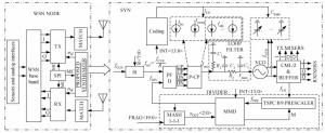
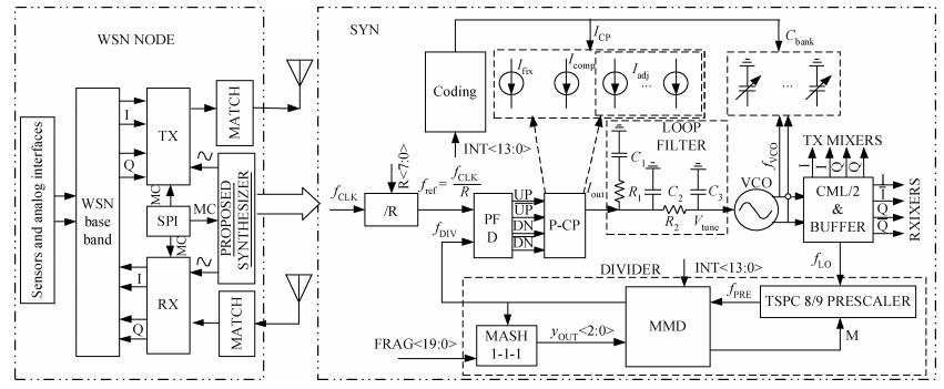
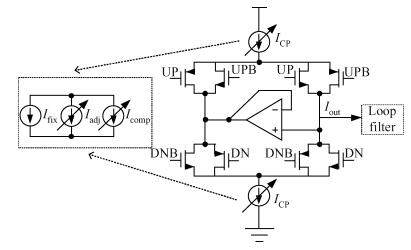
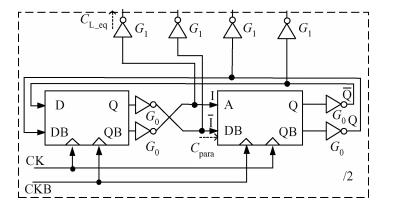
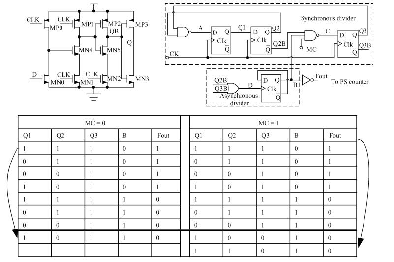
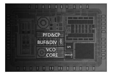
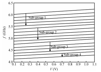
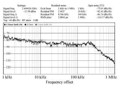
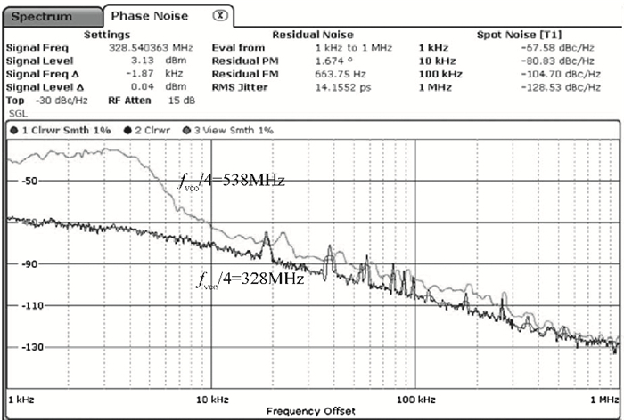
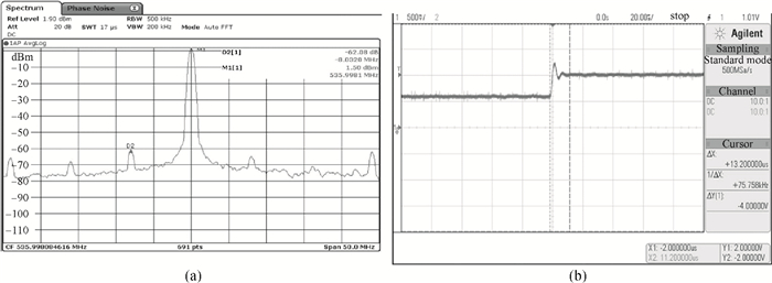
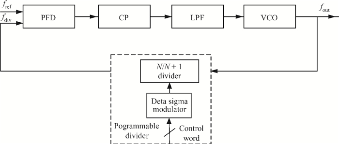
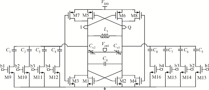
This paper presents a fractional-N frequency synthesizer for wireless sensor network (WSN) nodes. The proposed frequency synthesizer adopts a phase locked loop (PLL) based structure, which employs an LC voltage-controlled oscillator (VCO) with small VCO gain (KVCO) and frequency step (fstep) variations, a charge pump (CP) with current changing in proportion with the division ratio and a 20-bit Δ Σ modulator, etc. To realize constant KVCO and fstep, a novel capacitor sub-bands grouping method is proposed. The VCO sub-groups' sizes are arranged according to the maximal allowed KVCO variation of the system. Besides, a current mode logic divide-by-2 circuit with inside-loop buffers ensures the synthesizer generates I/Q quadrature signals robustly. This synthesizer is implemented in a 0.13 μm CMOS process. Measurement results show that the frequency synthesizer has a frequency span from 2.07 to 3.11 GHz and the typical phase noise is -86.34 dBc/Hz at 100 kHz offset and -114.17 dBc/Hz at 1 MHz offset with a loop bandwidth of about 200 kHz, which meet the WSN nodes' requirements.


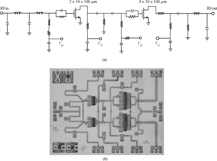
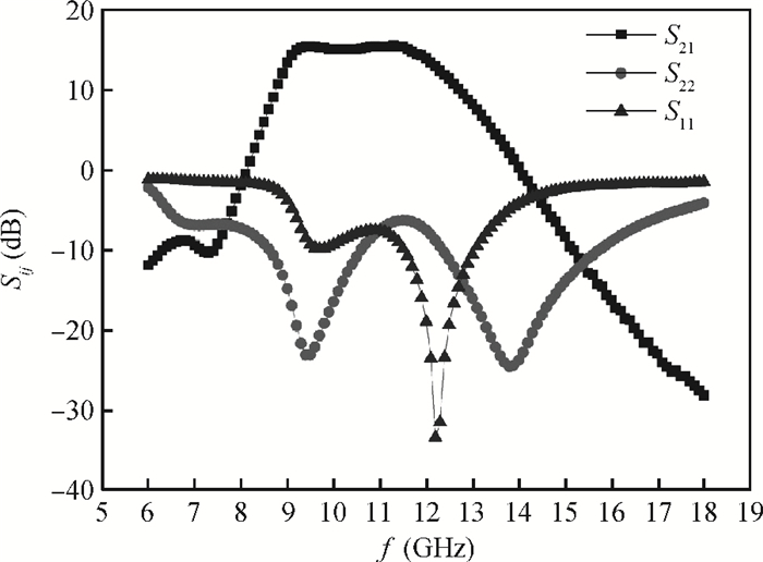
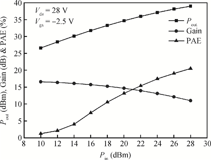
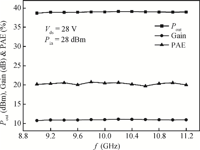
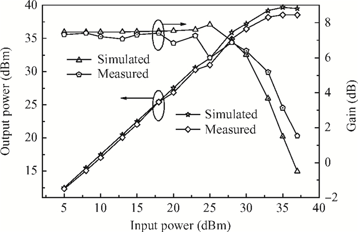
A flat gain two-stage MMIC power amplifier with a 2.8 GHz bandwidth is successfully developed for X band frequency application based on a fully integrated micro-strip AlGaN/GaN HEMT technology on a semi-insulating SiC substrate. Designed with a binary-cluster matching structure integrated with RC networks and LRC networks, the developed power MMIC gets a very flat small signal gain of 15 dB with a gain ripple of 0.35 dB over 9.1-11.9 GHz at the drain bias of 20 V. These RC networks are very easy to improve the stability of used GaN HEMTs with tolerance to the MMIC technology. Inside the frequency range of 9-11.2 GHz where the measurement system calibrated, the amplifier delivers a pulsed output power of 39 dBm and an associated power added efficiency of about 20% at 28 V without saturation, as the available RF power is limited.
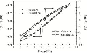
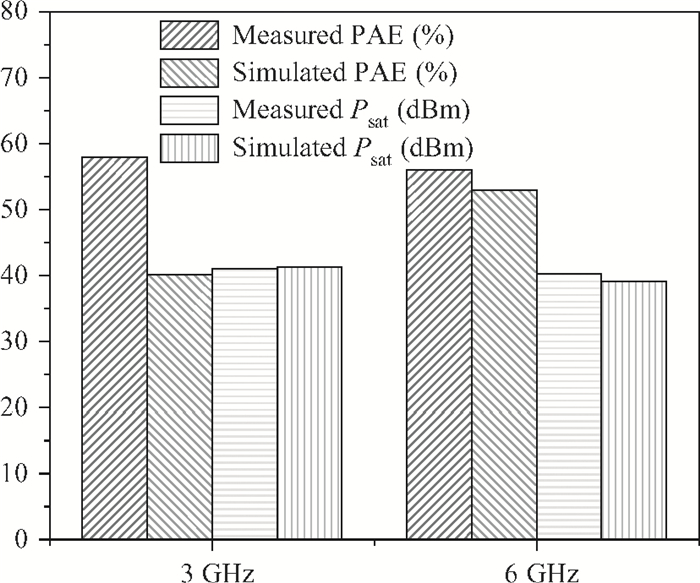
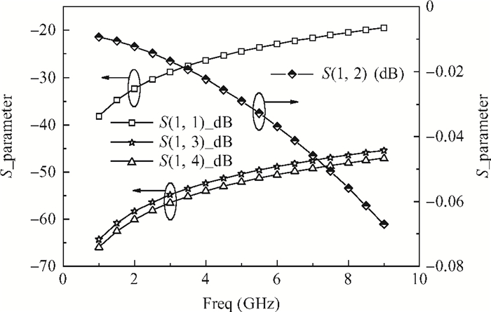
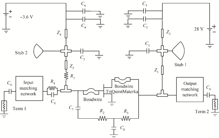
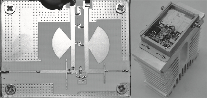
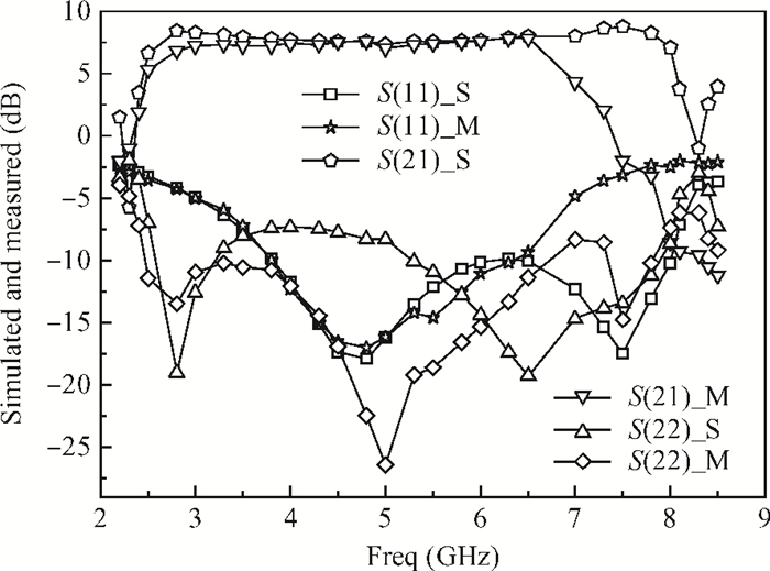
The design and fabrication of an ultra-broadband power amplifier based on a GaN HEMT, which operates in the frequency range from 3 to 8 GHz, is presented in this paper. A TGF2023-02 GaN HEMT chip from TriQuint is adopted and modeled. A novel negative feedback structure is applied in the circuit. The measured results show that the amplifier module has a wide range frequency response that is almost consistent with those of simulation at frequencies from 3 to 6.5 GHz. The measured power gain is greater than 7 dB between 3 and 6.5 GHz. The saturated output power is 38.5 dBm under DC bias of Vds=28 V, Vgs=-3.5 V at the frequency of 5.5 GHz.

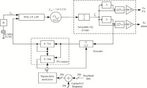
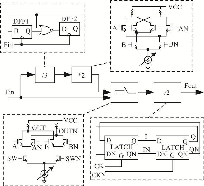
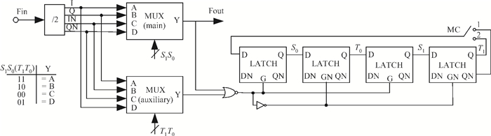
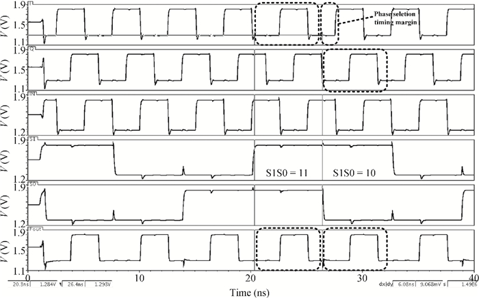
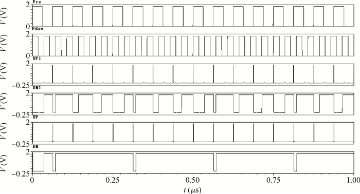
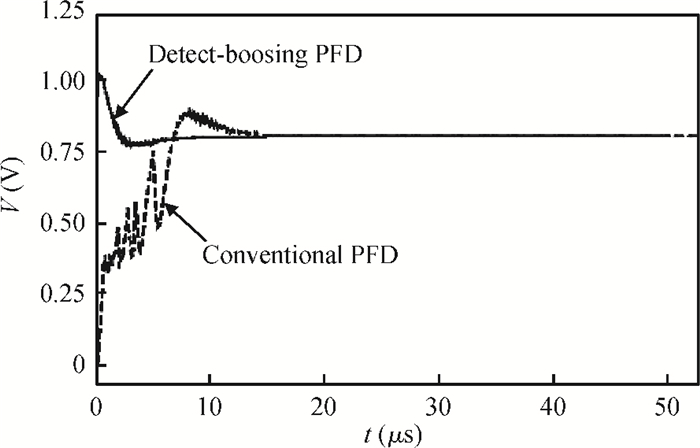
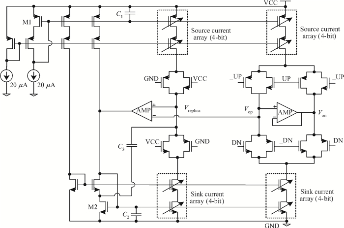
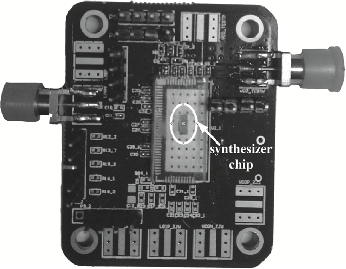
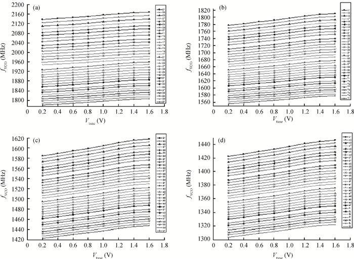
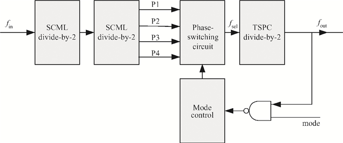
This paper presents a low phase-noise fractional-N frequency synthesizer which provides an in-phase/quadrature-phase (I/Q) signal over a frequency range of 220-1100 MHz for wireless networks of industrial automation (WIA) applications. Two techniques are proposed to achieve the wide range. First, a 1.4-2.2 GHz ultralow gain voltage-controlled oscillator (VCO) is adopted by using 128 tuning curves. Second, a selectable I/Q divider is employed to divide the VCO frequency by 2 or 3 or 4 or 6. Besides, a phase-switching prescaler is proposed to lower PLL phase noise, a self-calibrated charge pump is used to suppress spur, and a detect-boosting phase frequency detector is adopted to shorten settling time. With a 200 kHz loop bandwidth, lowest measured phase noise is -106 dBc/Hz at a 10 kHz offset and -131 dBc/Hz at a 1 MHz offset. Fabricated in the TSMC 0.18 μm CMOS process, the synthesizer occupies a chip area of 1.2 mm2, consumes only 15 mW from the 1.8 V power supply, and settles within 13.2 μs. The synthesizer is optimized for the WIA applications, but can also be used for other short-range wireless communications, such as 433, 868, 916 MHz ISM band applications.


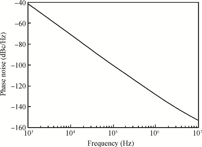
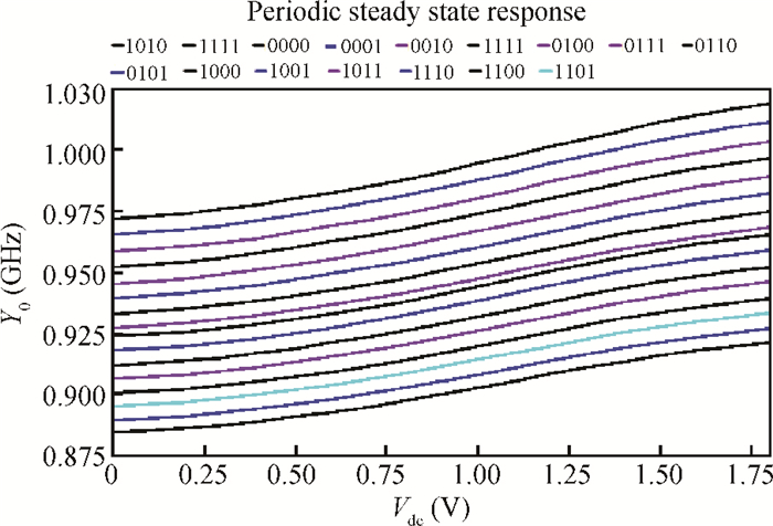
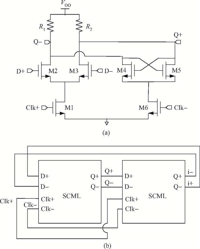
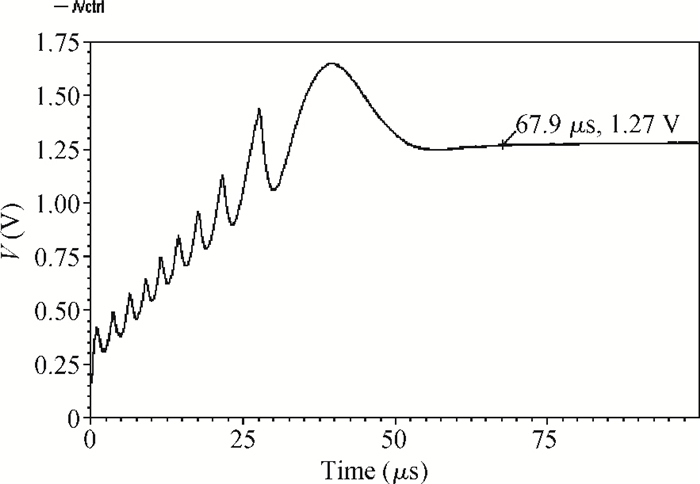
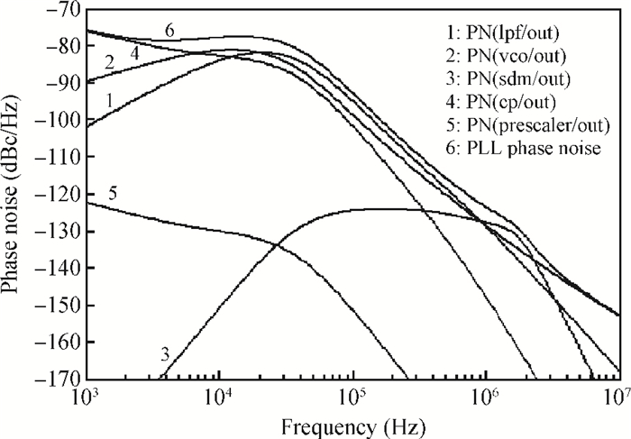
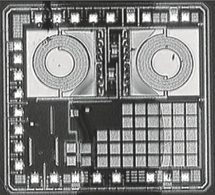
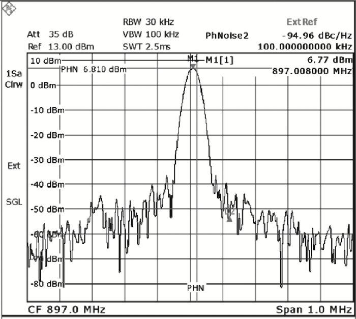
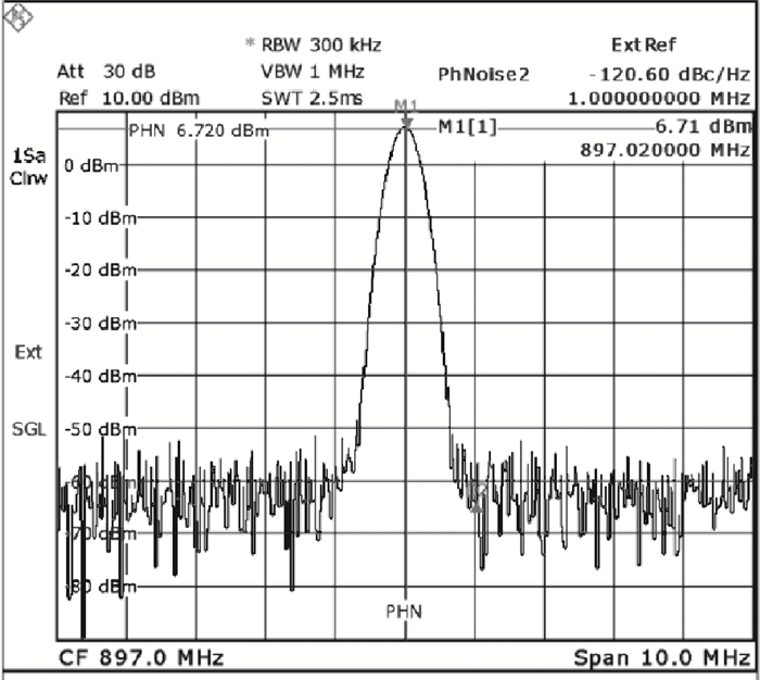
A 900 MHz fractional-N synthesizer is designed for the UHF transceiver. The VCO with a 4 bits capacitor bank covers 823-1061 MHz that implements 16 (24) sub-bands. A 7/8 dual-modulus prescaler is implemented with a phase-switching circuit and high-speed flip-flops, which are composed of source coupled logic. The proposed synthesizer phase-locked loop is demonstrated with a 50 kHz band width by a low 12.95 MHz reference clock, and offers a better phase noise and band width tradeoff. To reduce the out-band phase noise, a 4-levels 3-order single-loop sigma-delta modulator is applied. When its relative frequency resolution is settled to 10-6, the testing results show that the phase noises are -120.6 dBc/Hz at 1 MHz and -95.0 dBc/Hz at 100 kHz. The chip is 2.1 mm2 in UMC 0.18 μm CMOS. The power is 36 mW at a 1.8 V supply.

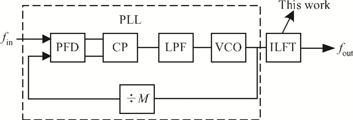
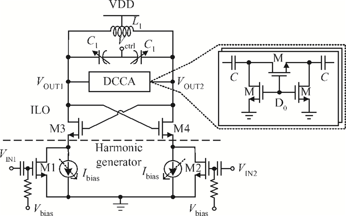
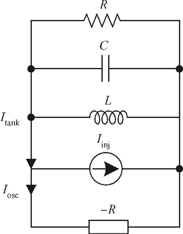
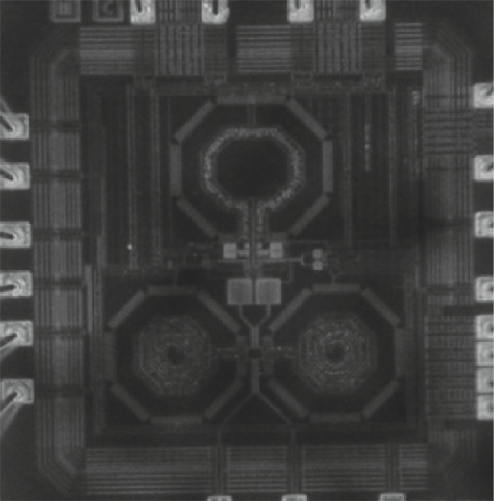
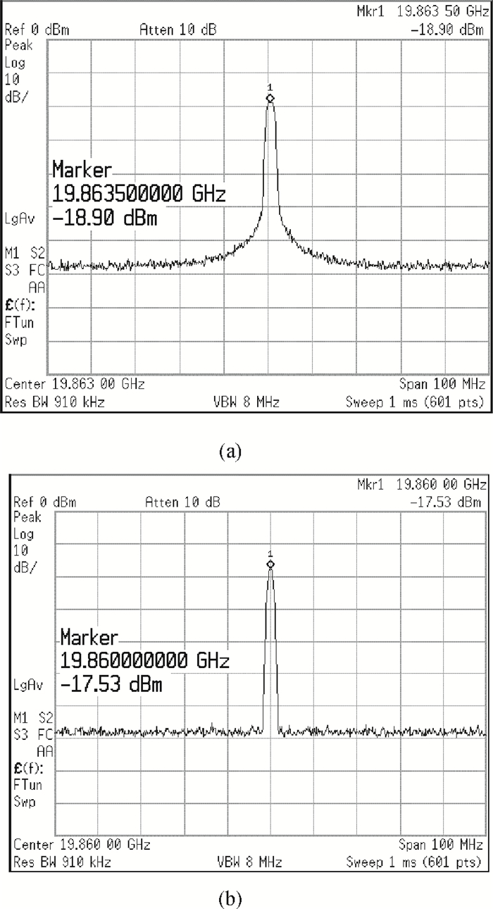
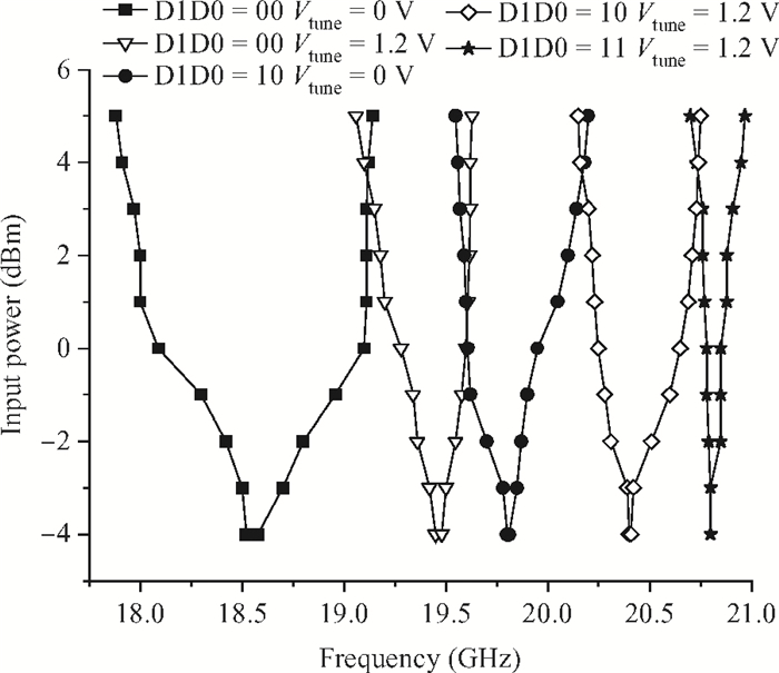
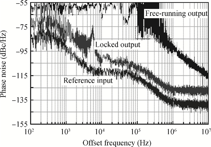
This paper presents a wide locking range and low DC power injection-locked frequency tripler for Kband frequency synthesizers application.The proposed ILFT employs a variable current source to decouple the injection signal path and the bias current so that the third harmonic of the injection signal can be maximized to enlarge the locking range.Meanwhile, a 2-bit digital control capacity array is used to further increase the output frequency locking range.It is implemented in a 130-nm CMOS process and occupies a chip area of 0.7×0.8 mm2 without pads.The measured results show that the proposed ILFT can achieve a whole locking range from 18 to 21 GHz under the input signal of 4 dBm and the core circuit dissipates only 4 mW of DC power from a 0.8 V supply voltage.The measured phase noise degradation from that of the injection signal is only 10 dB at 1 MHz offset.

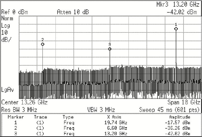
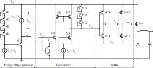
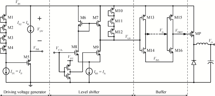
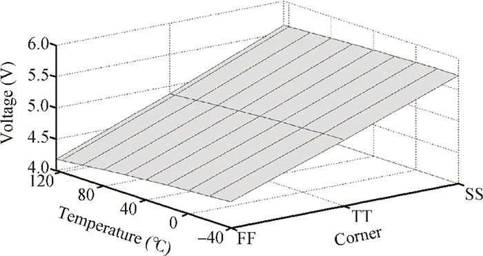
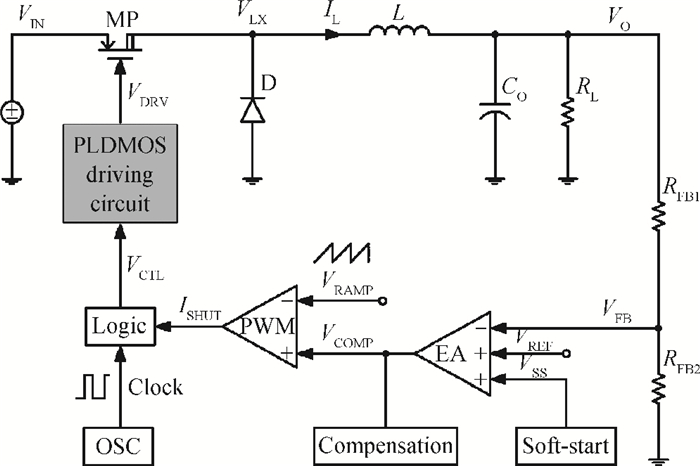
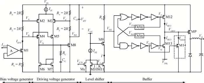
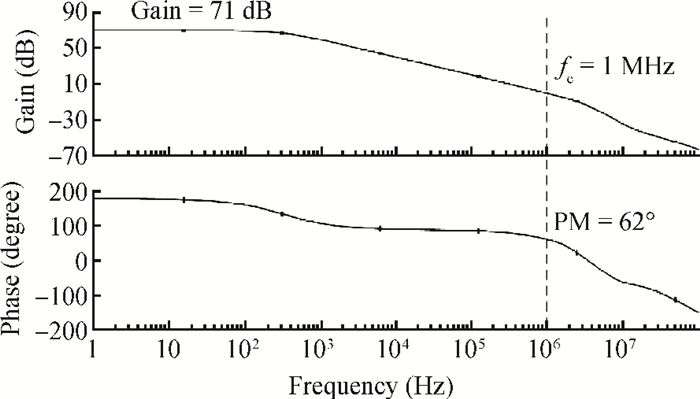
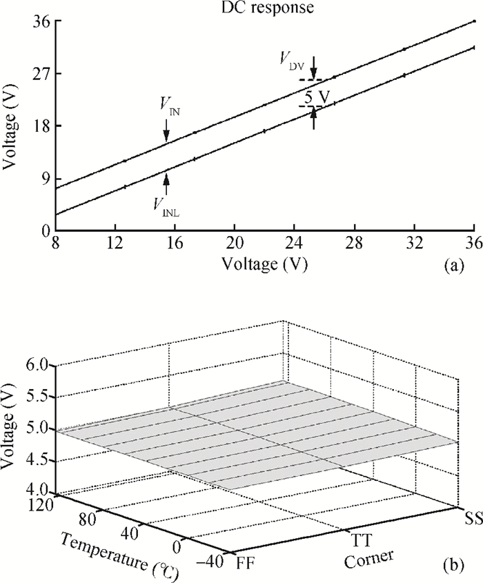
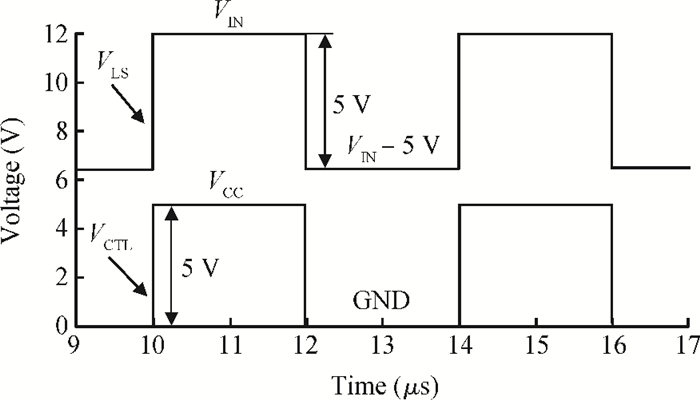
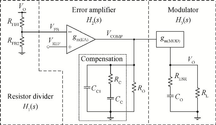
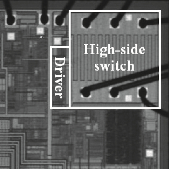
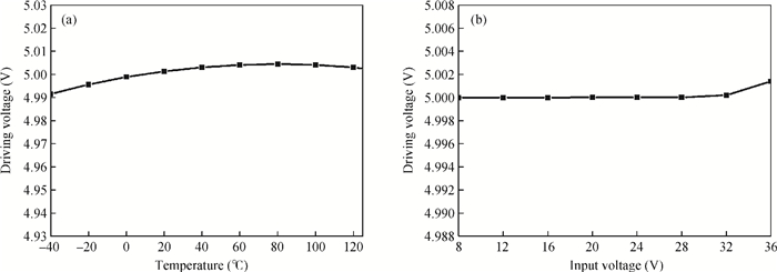
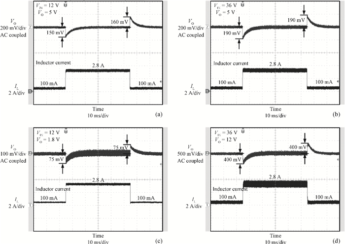
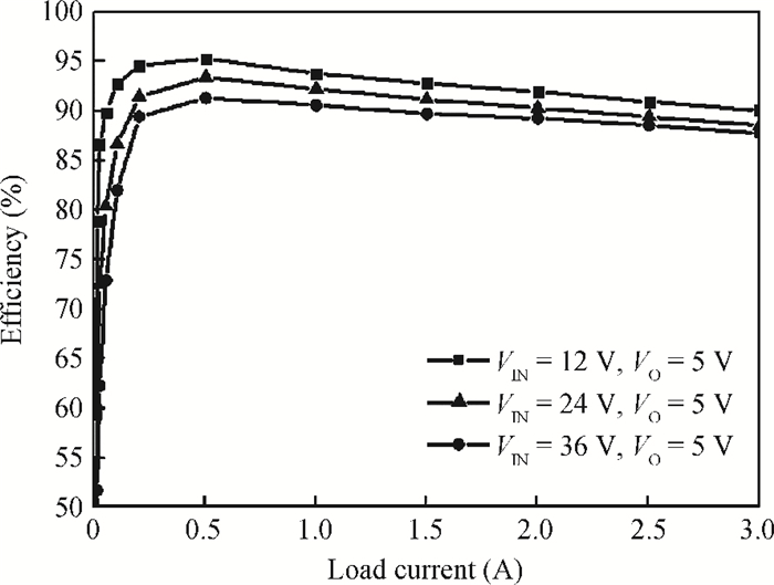
This paper presents a novel driving circuit for the high-side switch of high voltage buck regulators. A 40 V P-channel lateral double-diffused metal-oxide-semiconductor device whose drain-source and drain-gate can resist high voltage, but whose source-gate must be less than 5 V, is used as the high-side switch. The proposed driving circuit provides a stable and accurate 5 V driving voltage for protecting the high-side switch from breakdown and achieving low on-resistance and simple loop stability design. Furthermore, the driving circuit with excellent driving capability decreases the switching loss and dead time is also developed to reduce the shoot-through current loss. Therefore, power efficiency is greatly improved. An asynchronous buck regulator with the proposed technique has been successfully fabricated by a 0.35 μm CDMOS technology. From the results, compared with the accuracy of 16.38% of the driving voltage in conventional design, a high accuracy of 1.38% is achieved in this work. Moreover, power efficiency is up to 95% at 12 V input and 5 V output.


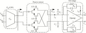
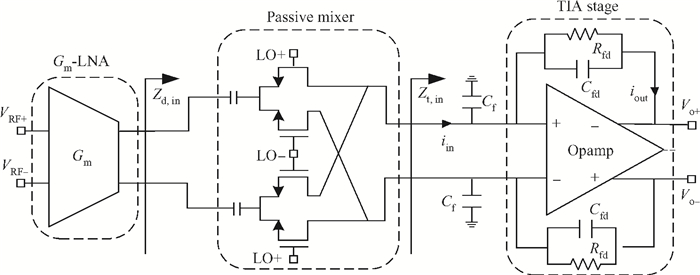
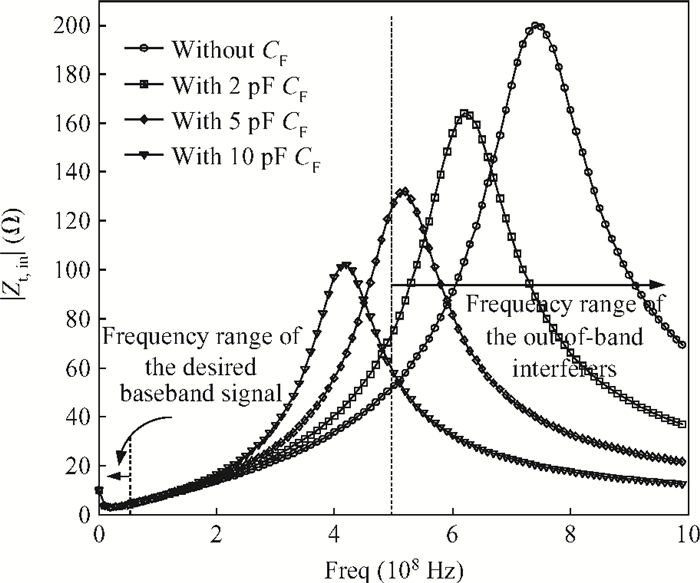
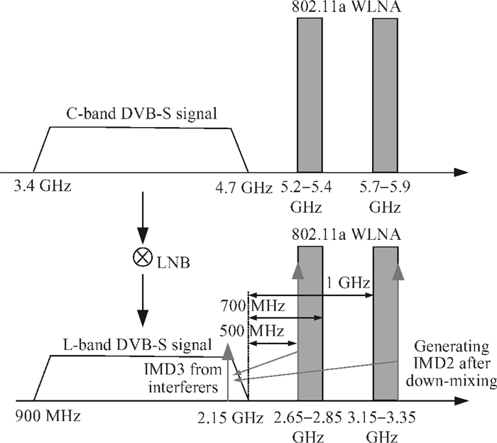
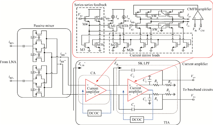
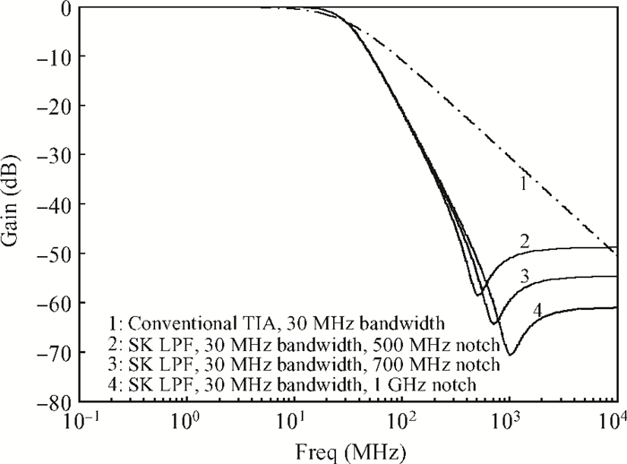
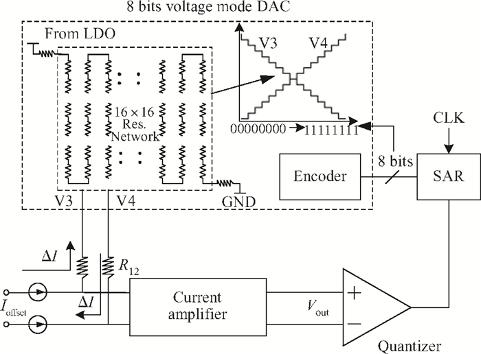
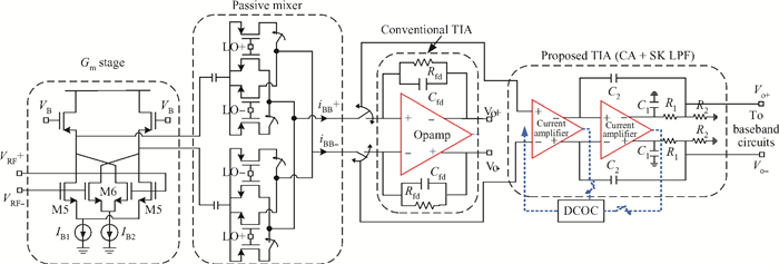
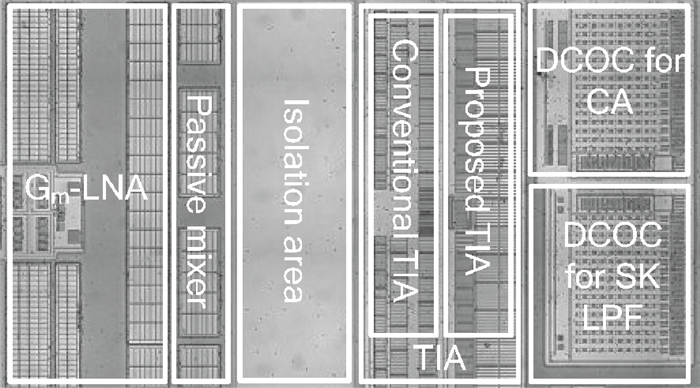
An integrated downconverter with high linearity for digital broadcasting system receivers is implemented in a 0.13 μm CMOS process with an active area of 0.1 mm2. The current-mode scheme is adopted to improve linearity performance by avoiding voltage fluctuation. A passive CMOS switching pair is utilized to improve the even-order linearity of the downconverter. A current amplifier is used to provide low input impedance which will easily lead to a wide operating bandwidth and high linearity. Moreover, a current-mode Sallen-Key low-pass filter is adopted for effective rejection of out-of-band interferers and also low input impedance. The digital-assisted DC offset calibration improves the second-order distortion of the downconverter. This design achieves a maximum gain of 40 dB and a dynamic range of 10 dB. Measured noise figure is 8.2 dB, an ⅡP2 of 63 dBm, an ⅡP3 of 17 dBm at the minimum gain of 30 dB. The downconverter consumes about 7.7 mA under a supply of 1.2 V.

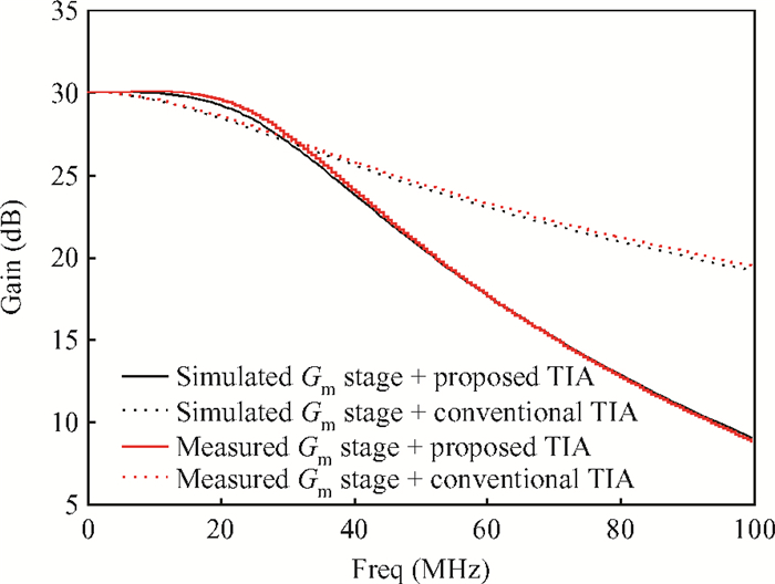


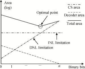
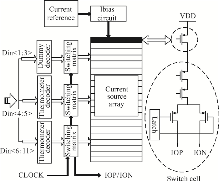
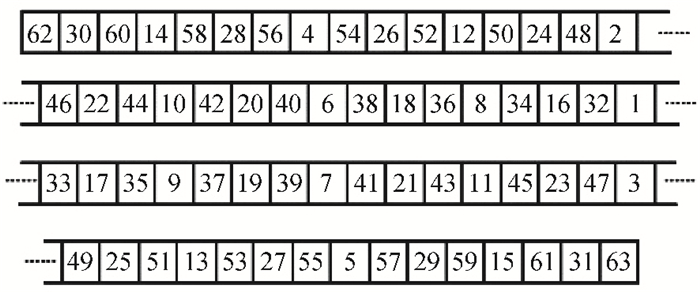
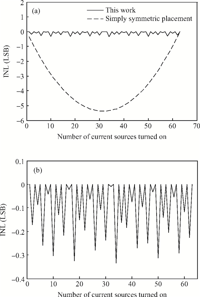
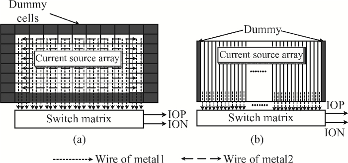
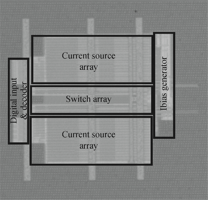
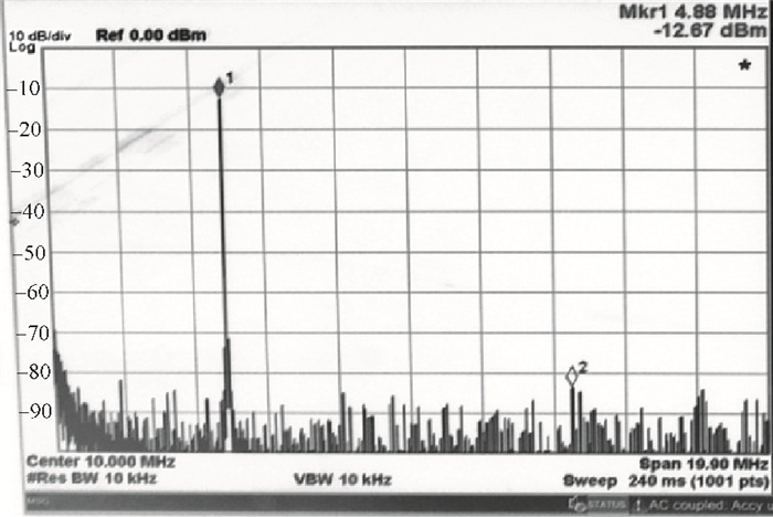
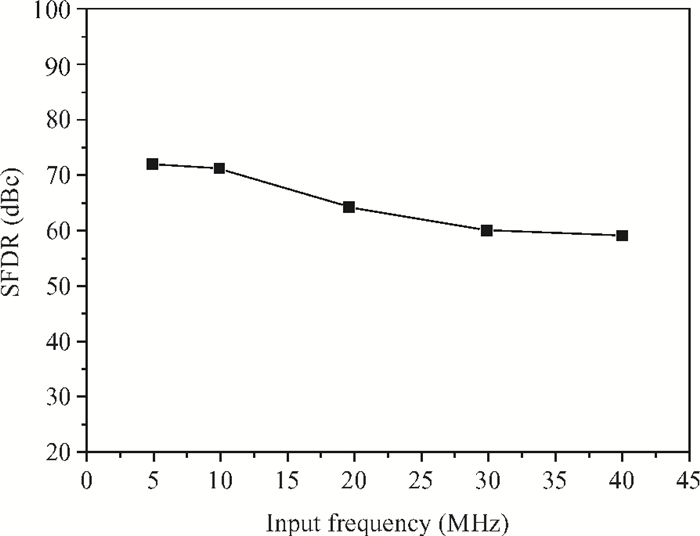
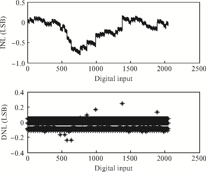
This paper presents an 11-bit 160 MS/s 2-channel current-steering digital-to-analog converter (DAC) IP. The circuit and layout are carefully designed to optimize its performance and area. A 6-2-3 segmented structure is used for the trade-off among linearity, area and layout complexity. The sizes of current source transistors are calculated out according to the process matching parameter. The unary current cells are placed in a one-dimension distribution to simplify the layout routing, spare area and wiring layer. Their sequences are also carefully designed to reduce integral nonlinearity. The test result presents an SFDR of 72 dBc at 4.88 MHz input signal with DNL ≤ 0.25 LSB, INL ≤ 0.8 LSB. The full-scale output current is 5 mA with a 2.5 V analog power supply. The core of each channel occupies 0.08 mm2 in a 1P-8M 55 nm CMOS process.

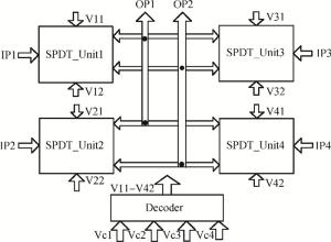
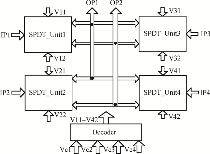
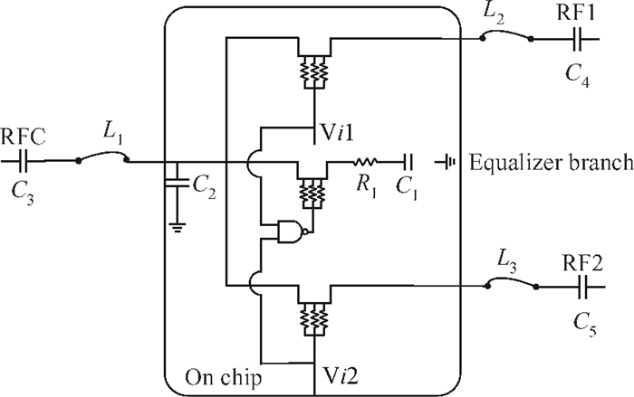
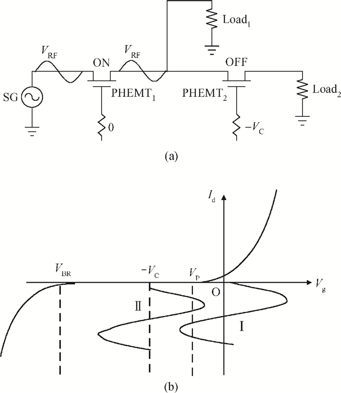
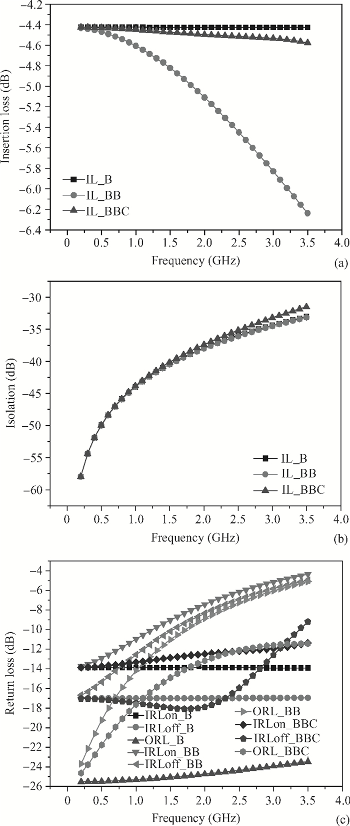
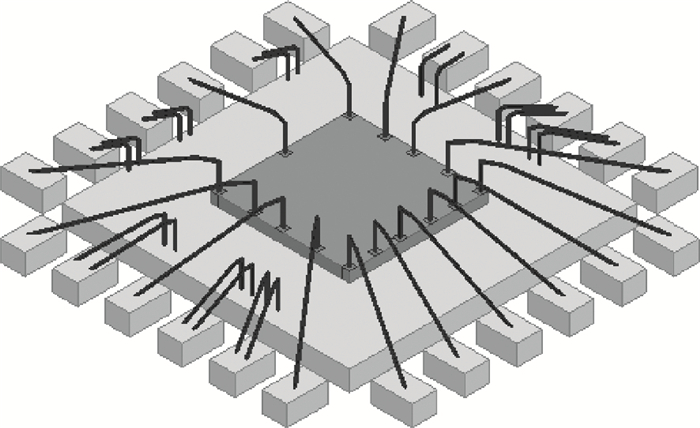
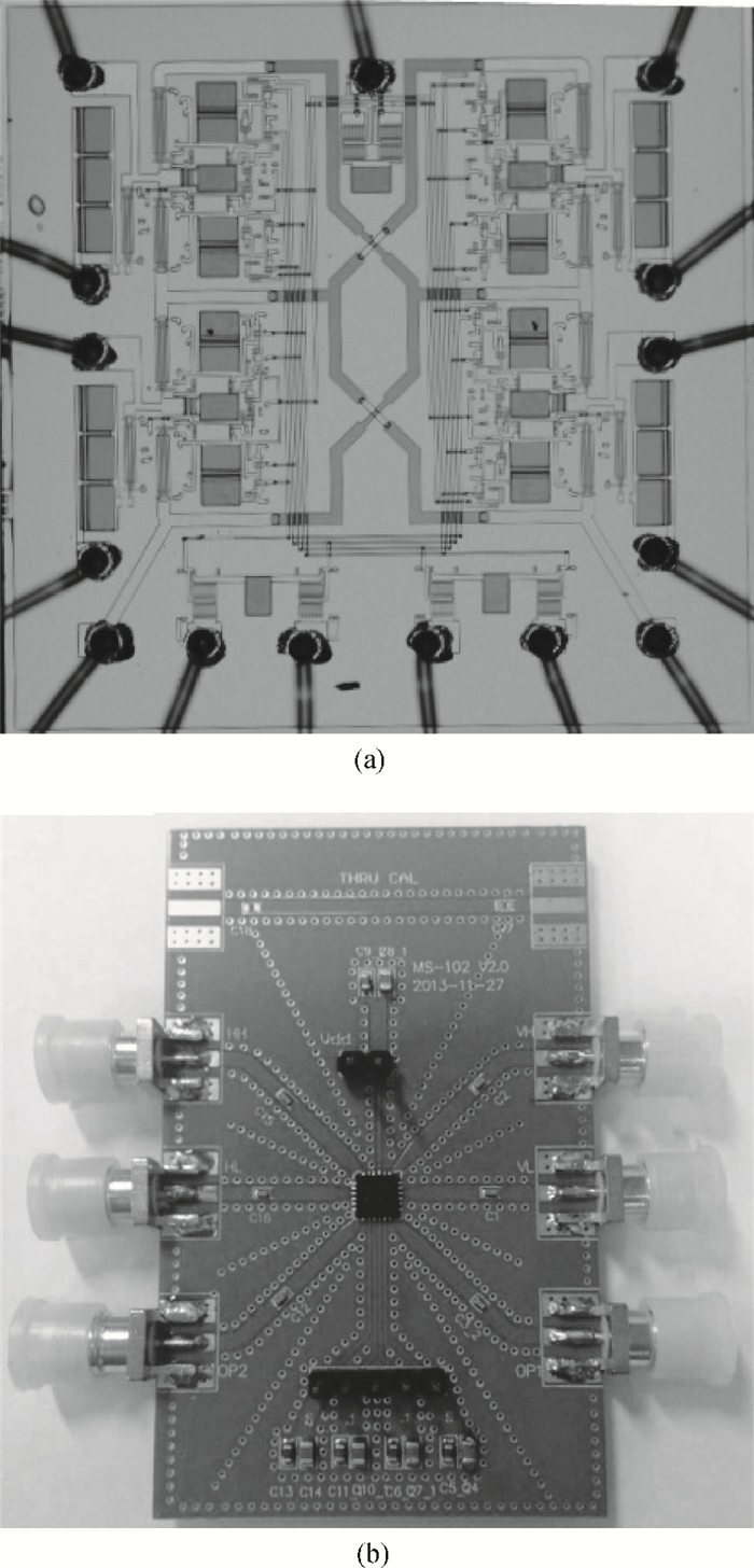
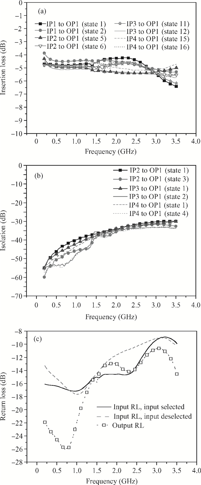
This paper presents a 4×2 switching matrix implemented in the Win 0.5 μm GaAs pseudomorphic high electron mobility transistor process, it covers the 0.5-3 GHz frequency range. The switch matrix is composed of 4 SPDT switch whose two output ports can simultaneously select the input port and a 4 to 8 bit digital decoder, both the radio frequency (RF) part and the digital part are integrated into one single chip. The chip is packaged in a low cost QFN24 plastic package. On chip shunt, capacitors at the input ports are taken to compensate for the bonding wire inductance effect. The designed switch matrix shows a good measured performance:the insertion loss is less than 5.5 dB, the isolation is no worse than 30 dB, the return loss of input ports and output ports is better than -10 dB, the input 1 dB compression point is better than 25.6 dBm, and the OIP3 is better than 37 dBm. The chip size of the switch matrix is only 1.45×1.45 mm2.
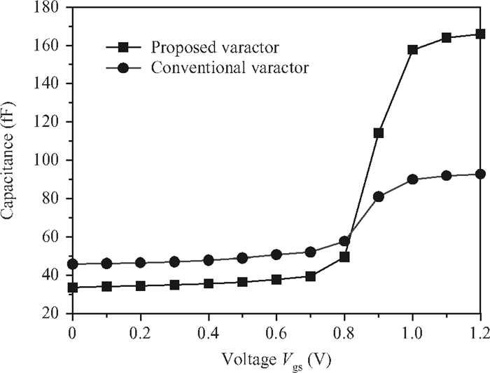
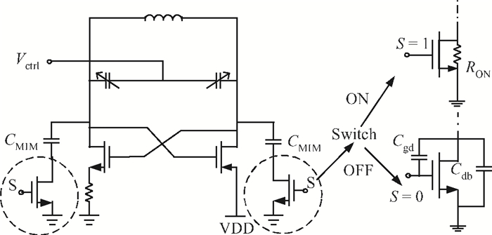
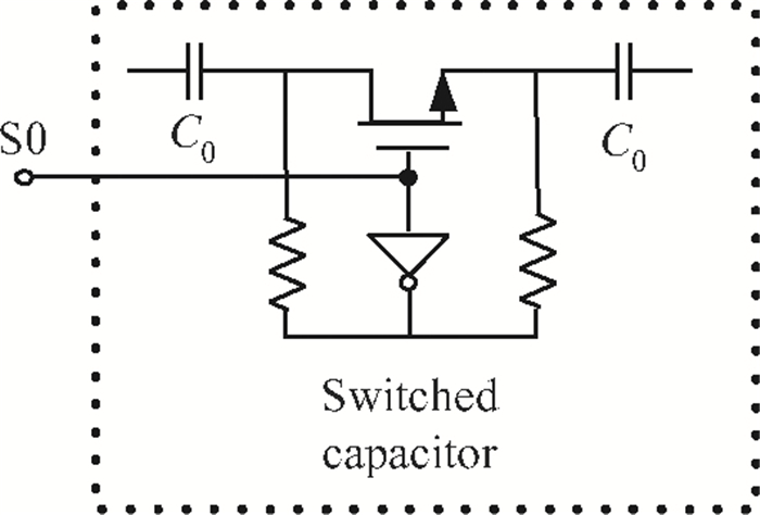
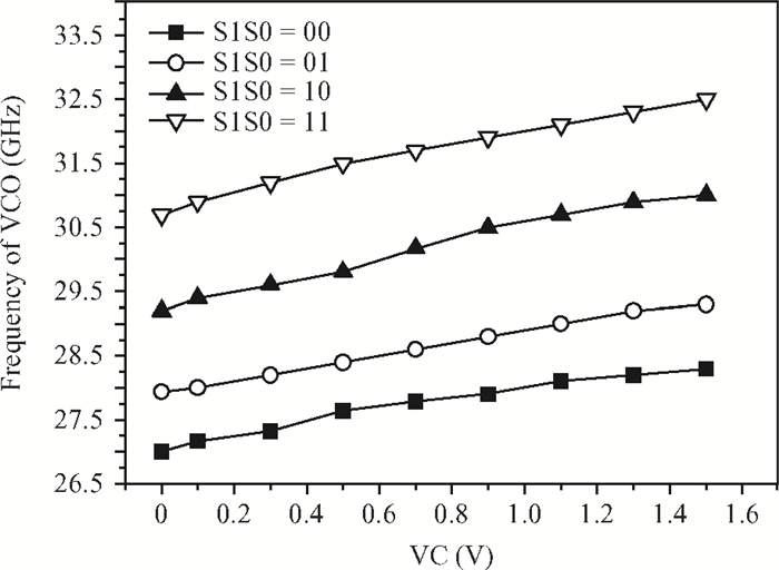
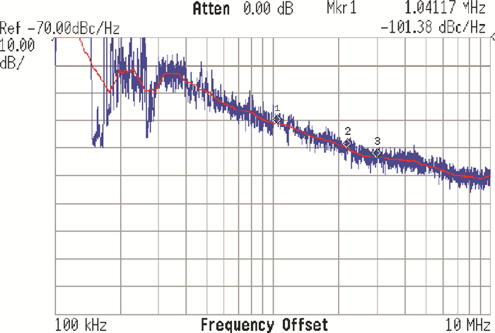
A low power VCO with a wide tuning range and low phase noise has been designed and realized in a standard 90 nm CMOS technology. A newly proposed current-reuse cross-connected pair is utilized as a negative conductance generator to compensate the energy loss of the resonator. The supply current is reduced by half compared to that of the conventional LC-VCO. An improved inversion-mode MOSFET (IMOS) varactor is introduced to extend the capacitance tuning range from 32.8% to 66%. A detailed analysis of the proposed varactor is provided. The VCO achieves a tuning range of 27-32.5 GHz, exhibiting a frequency tuning range (FTR) of 18.4% and a phase noise of -101.38 dBc/Hz at 1 MHz offset from a 30 GHz carrier, and shows an excellent FOM of -185 dBc/Hz. With the voltage supply of 1.5 V, the core circuit of VCO draws only 2.1 mA DC current.


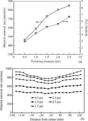
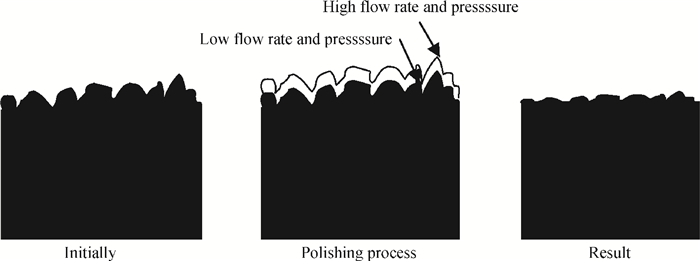
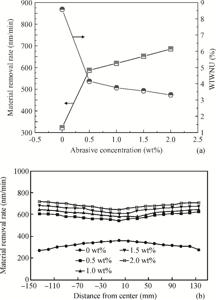
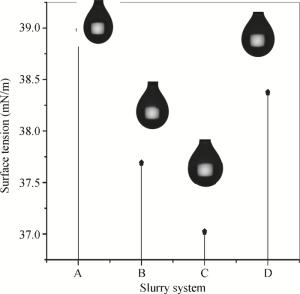
Chemical mechanical planarization (CMP) is a critical process in deep sub-micron integrated circuit manufacturing. This study aims to improve the planarization capability of slurry, while minimizing the mechanical action of the pressure and silica abrasive. Through conducting a series of single-factor experiments, the appropriate pressure and the optimum abrasive concentration for the alkaline slurry were confirmed. However, the reduced mechanical action may bring about a decline of the polishing rate, and further resulting in the decrease of throughput. Therefore, we take an approach to compensating for the loss of mechanical action by optimizing the composition of the slurry to enhance the chemical action in the CMP process. So 0.5 wt% abrasive concentration of alkaline slurry for copper polishing was developed, it can achieve planarization efficiently and obtain a wafer surface with no corrosion defect at a reduced pressure of 1.0 psi. The results presented here will contribute to the development of a "softer gentler polishing" technique in the future.
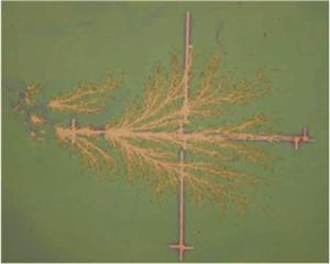
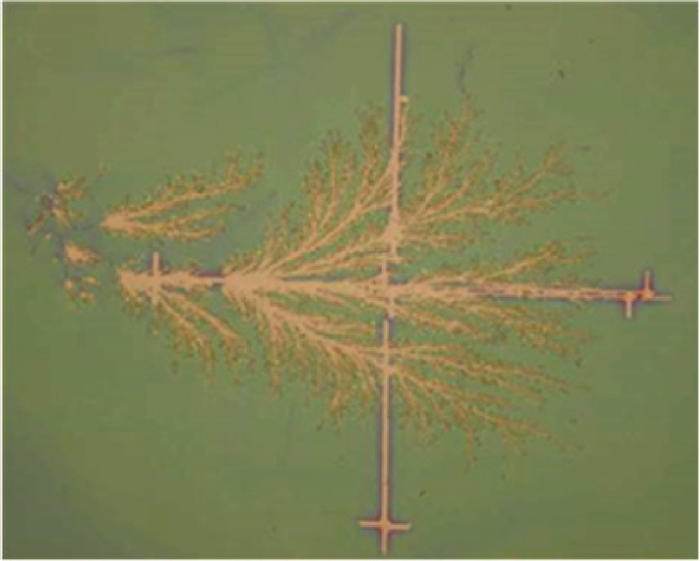
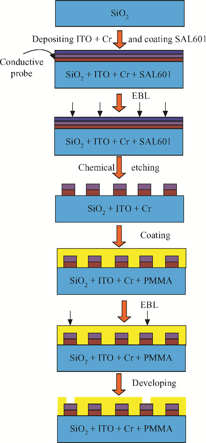
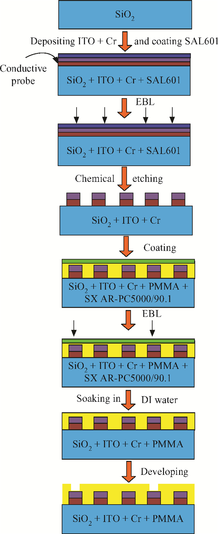
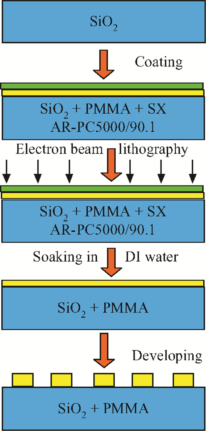
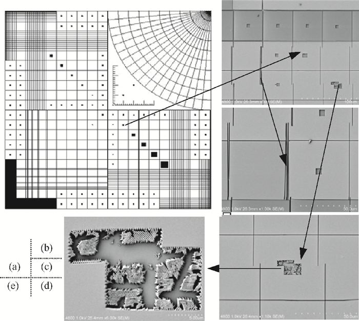
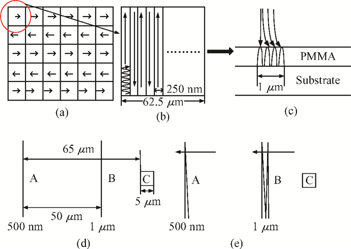
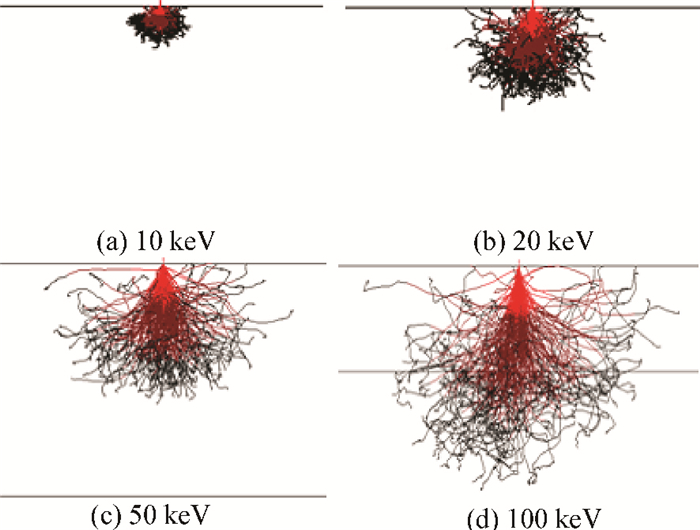
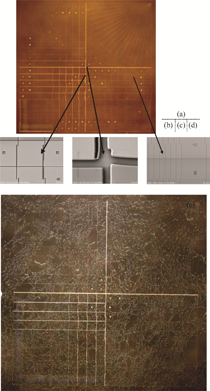
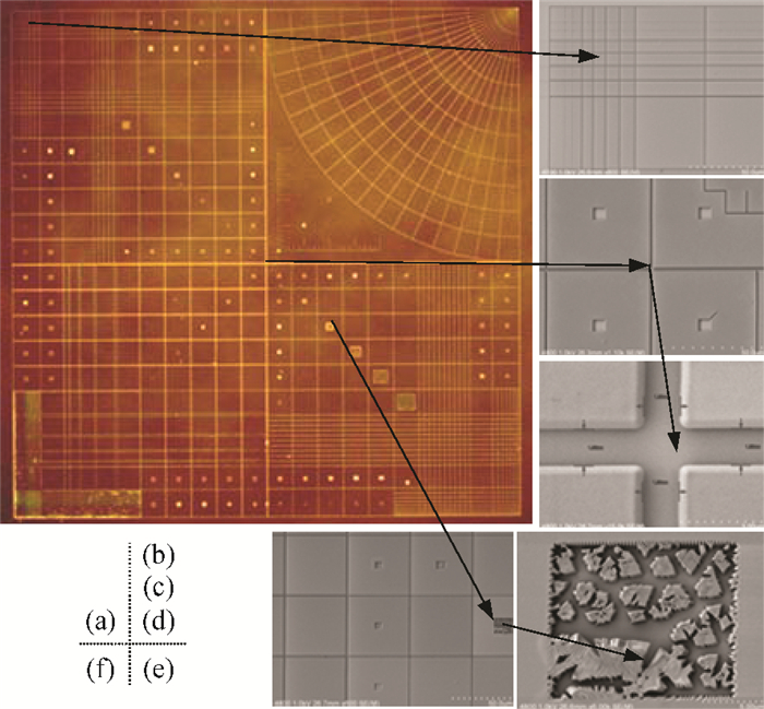
Pattern distortions caused by the charging effect should be reduced while using the electron beam lithography process on an insulating substrate. We have developed a novel process by using the SX AR-PC 5000/90.1 solution as a spin-coated conductive layer, to help to fabricate nanoscale patterns of poly-methyl-methacrylate polymer resist on glass for phased array device application. This method can restrain the influence of the charging effect on the insulating substrate effectively. Experimental results show that the novel process can solve the problems of the distortion of resist patterns and electron beam main field stitching error, thus ensuring the accuracy of the stitching and overlay of the electron beam lithography system. The main characteristic of the novel process is that it is compatible to the multi-layer semiconductor process inside a clean room, and is a green process, quite simple, fast, and low cost. It can also provide a broad scope in the device development on insulating the substrate, such as high density biochips, flexible electronics and liquid crystal display screens.
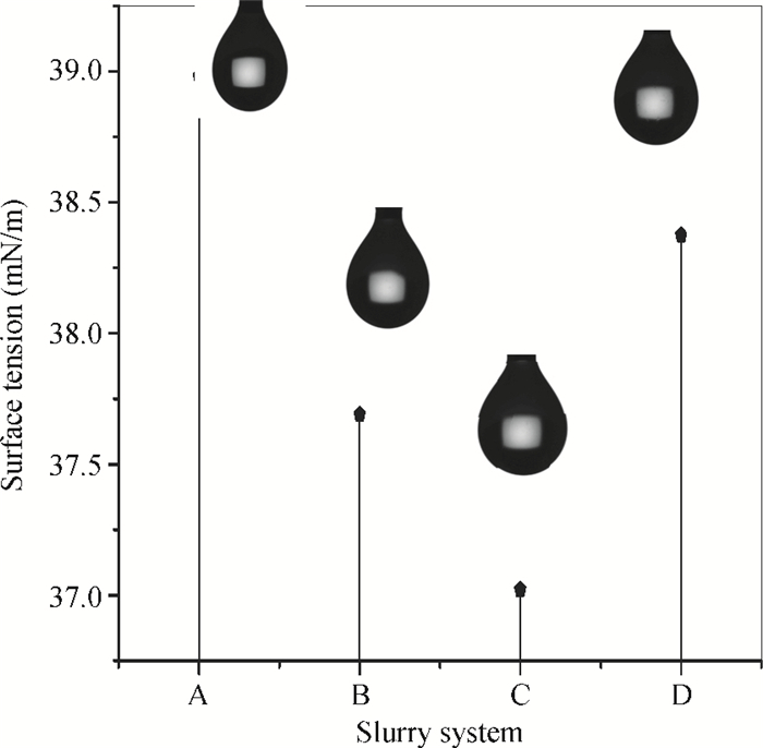
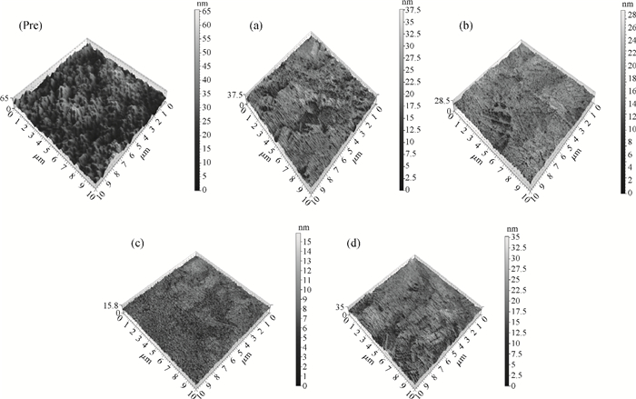
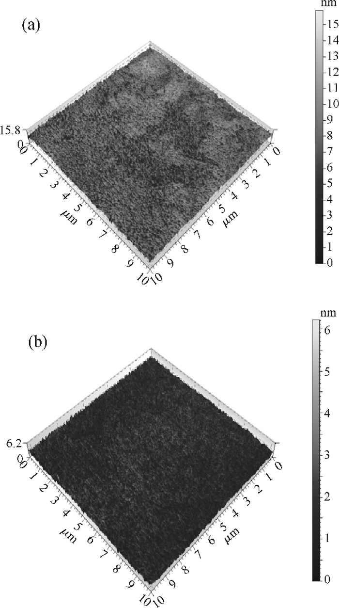
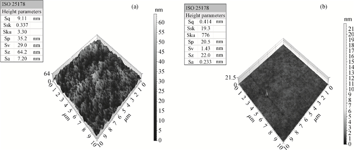
The surface roughness seriously affects the performance of devices after barrier CMP. Due to the high surface roughness of copper line, the local resistance of a device will be high when working, then the copper line will overheat prompting the generation of electro-migration and the circuit will lose efficacy. Reducing the surface roughness of the copper line in barrier CMP is still an important research topic. The main factors influencing the surface roughness of copper line in alkaline barrier slurry are analyzed in the paper. Aimed at influencing the law on the surface roughness of copper line, using a new type of alkaline barrier slurry with a different pH of the chelating agent and changing the content of non-ionic surfactant, we then analyze the influencing law both on the surface roughness of copper line, and the influence mechanism. The experimental results show that with a chelating agent with a low pH value in the barrier slurry, the surface roughness of the copper line is 1.03 nm and it is the lowest in all of the barrier slurries, and with the increase of non-ionic surfactant concentration, the surface roughness of copper line is reduced to 0.43 nm, meeting the demand of further development of integrated circuits.