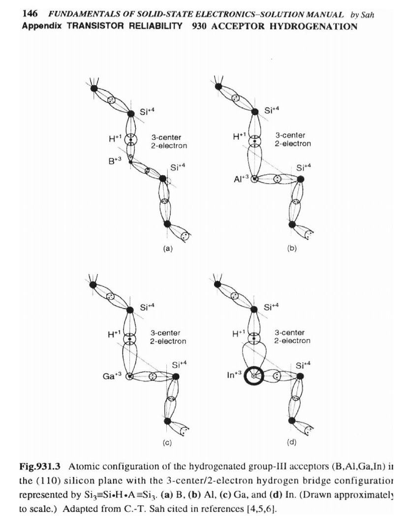
_mini.jpg)
The ‘abnormally’ high electrical conductivity of pure water was recently studied by us using our protonic bond, trap and energy band model, with five host particles:the positive and negative protons, and the amphoteric protonic trap in three charge states, positive, neutral and negative.Our second report described the electrical charge storage capacitance of pure and impure water.This third report presents the theory of particle density and electrical conductance of pure and impure water, including the impuritons, which consist of an impurity ion bonded to a proton, proton-hole or proton trap and which significantly affect impure waters' properties.
Issue Browser
Volume 35, Issue 4,
Apr 2014
.jpg)
.jpg)

J. Semicond.
2014, 35(4): 042001 doi: 10.1088/1674-4926/35/4/042001

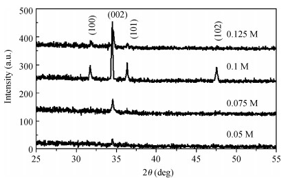
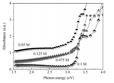
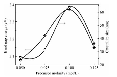
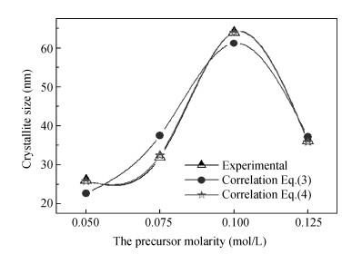
We investigated the structural and optical properties of ZnO thin films as an n-type semiconductor. The films were deposited at different precursor molarities using an ultrasonic spray method. In this paper we focused our attention on a new approach describing a correlation between the crystallite size and optical gap energy with the precursor molarity of ZnO thin films. The results show that the X-ray diffraction (XRD) spectra revealed a preferred orientation of the crystallites along the c-axis. The maximum value of the crystallite size of the films is 63.99 nm obtained at 0.1 M. The films deposited with 0.1 M show lower absorption within the visible wavelength region. The optical gap energy increased from 3.08 to 3.37 eV with increasing precursor molarity of 0.05 to 0.1 M. The correlation between the structural and optical properties with the precursor molarity suggests that the crystallite size of the films is predominantly influenced by the band gap energy and the precursor molarity. The measurement of the crystallite size by the model proposed is equal to the experimental data. The minimum error value was estimated by Eq. (4) in the higher crystallinity.
J. Semicond.
2014, 35(4): 042002 doi: 10.1088/1674-4926/35/4/042002
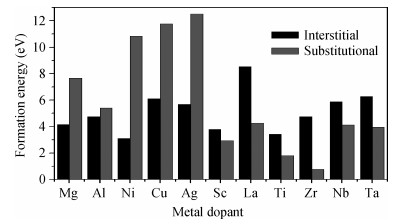
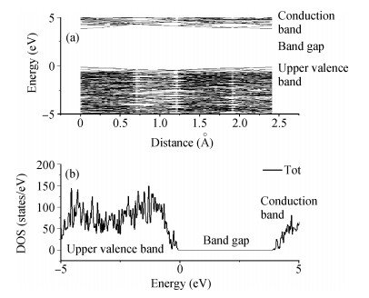
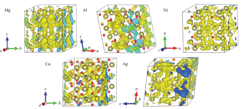
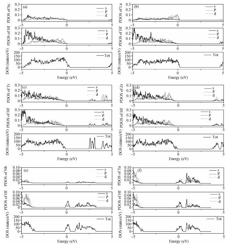
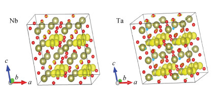
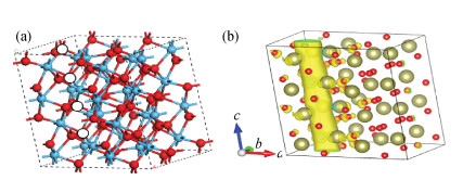
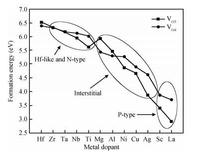
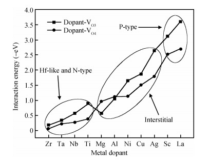
Based on density-functional theory (DFT), the effects of metal dopants in HfO2-based RRAM are studied by the Vienna ab initio simulation package (VASP). Metal dopants are classified into two types (interstitial and substitutional) according to the formation energy when they exist in HfO2 cell. Several conductive channels are observed through the isosurface plots of the partial charge density for HfO2 doped with interstitial metals, while this phenomenon cannot be found in HfO2 doped with substitutional metals. The electron density of states (DOS) and the projected electron density of states (PDOS) are calculated and analyzed; it is found that the conduction filament in HfO2 is directly formed by the interstitial metals and further, that the substitutional metals cannot directly generate conduction filament. However, all the metal dopants contribute to the formation of the oxygen vacancy (VO) filament. The formation energy of the VO and the interaction between metal dopants and Vo are calculated; it is revealed that the P-type substitutional metal dopants have a strong enhanced effect on the VO filament, the interstitial metal dopants have a minor assistant effect, while Hf-like and N-type substitutional metal dopants have the weakest assistant effect.

J. Semicond.
2014, 35(4): 043001 doi: 10.1088/1674-4926/35/4/043001

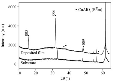
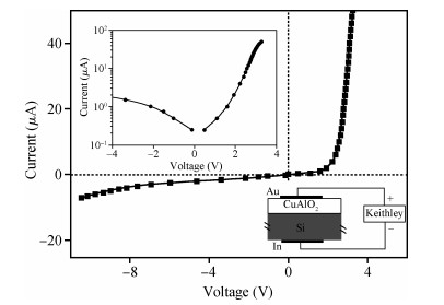
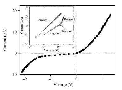
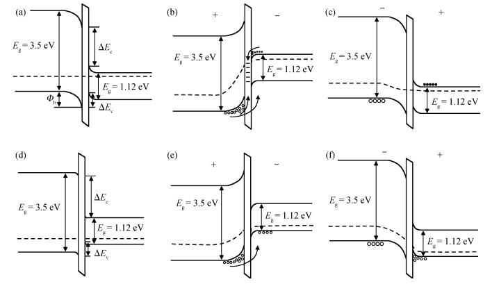
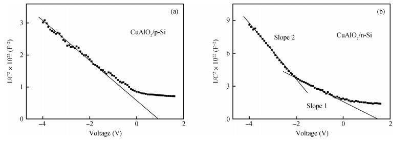
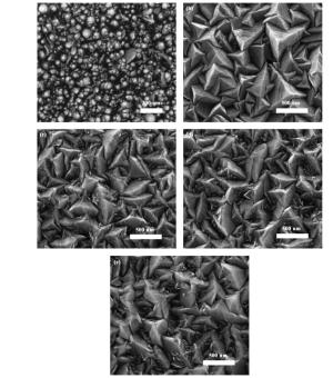
CuAlO2 thin films have been prepared by the chemical solution deposition method on both n-Si and p-Si substrates. X-ray diffraction analysis indicates that the obtained CuAlO2 films have a single delafossite structure. The current transport properties of the resultant p-CuAlO2/n-Si and p-CuAlO2/p-Si heterojunctions are investigated by current-voltage measurements. The p-CuAlO2/n-Si has a rectifying ratio of~35 within the applied voltages of -3.0 to +3.0 V, while the p-CuAlO2/p-Si shows Schottky diode-like characteristics, dominated in forward bias by the flow of space-charge-limited current.

J. Semicond.
2014, 35(4): 043002 doi: 10.1088/1674-4926/35/4/043002
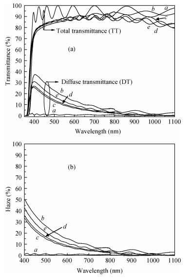
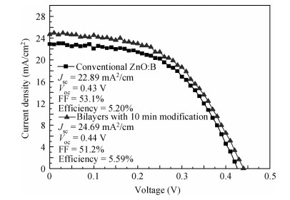
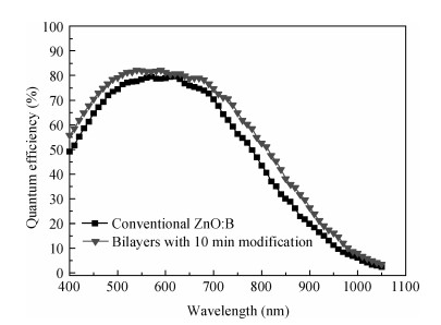
Modified textured surface boron-doped ZnO (ZnO:B) transparent conductive layers for thin-film solar cells were fabricated by low-pressure metal organic chemical vapor deposition (LP-MOCVD) on glass substrates. These modified textured surface ZnO:B thin films included two layers. The first ZnO:B layer, which has a pyramid-shaped texture, was deposited under conventional growth conditions, and the second layer, which has a sphere-like structure, at a relatively lower growth temperature. Typical bi-layer ZnO:B thin films exhibit a high electron mobility of 27.6 cm2/(V· s) due to improved grain boundary states. For bi-layer ZnO:B, the haze value increases and the total transmittance decreases with the increasing film thickness of the second modification layer. When applied in hydrogenated microcrystalline silicon (μc-Si:H) thin-film solar cells, the modified textured surface ZnO:B layers present relatively higher conversion efficiency than conventional ZnO:B films.

J. Semicond.
2014, 35(4): 043003 doi: 10.1088/1674-4926/35/4/043003
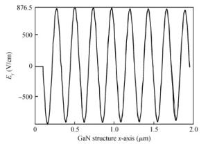
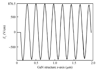
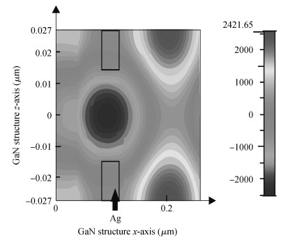
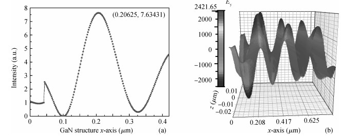
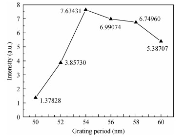
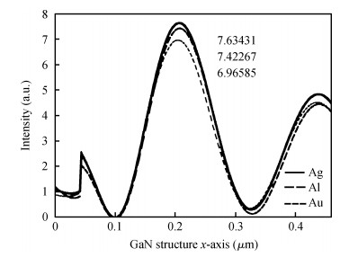
The transmitting light in GaN-based LED with 30 nm thickness metal film grating is investigated. We proposed a basic grating structure model to enhance light intensity in GaN material, which was simpler and cheaper. We calculated and analyzed the structure with different parameters, and studied the numerical simulation results of Ag-films/Al-films/Au-films. With a simple Al or Ag basic grating structure, the 7.4-7.6 times intensity of 550 nm light can be obtained easily, and the enhancement efficiency is better than others.


J. Semicond.
2014, 35(4): 044001 doi: 10.1088/1674-4926/35/4/044001
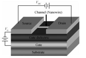
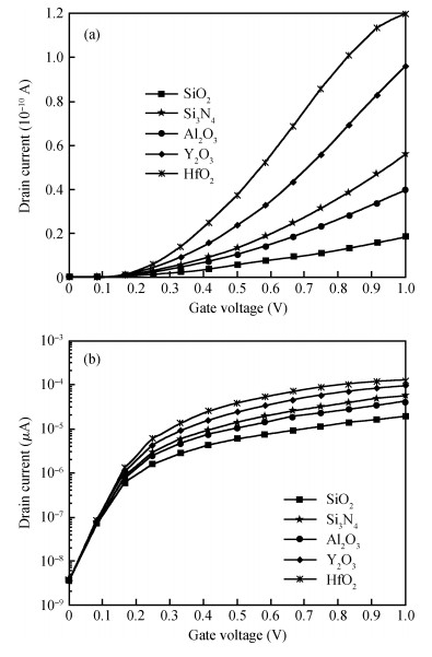
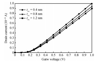
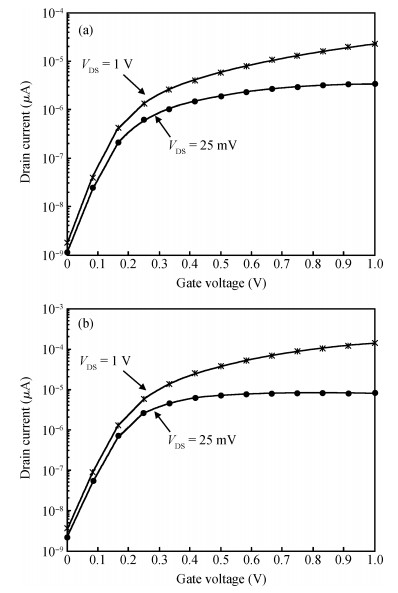
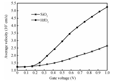
We have analyzed the effective oxide thickness (EOT) of the dielectric material for which we have optimum performance and the output characteristics of the silicon nanowire transistors by replacing the traditional SiO2 gate insulator with a material that has a much higher dielectric constant (high-k) gate, materials like Si3N4, Al2O3, Y2O3 and HfO2. We have also analyzed the channel conductance, the effect of a change in thickness, the average velocity of the charge carrier and the conductance efficiency in order to study the performance of silicon nanowire transistors in the nanometer region. The analysis was performed using the Fettoy, a numerical simulator for ballistic nanowire transistors using a simple top of the barrier (Natori) approach, which is composed of several matlab scripts. Our results show that hafnium oxide (HfO2) gate insulator material provides good thermal stability, a high recrystallization temperature and better interface qualities when compared with other gate insulator materials; also the effective oxide thickness of HfO2 is found to be 0.4 nm.

J. Semicond.
2014, 35(4): 044002 doi: 10.1088/1674-4926/35/4/044002
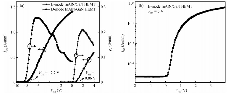
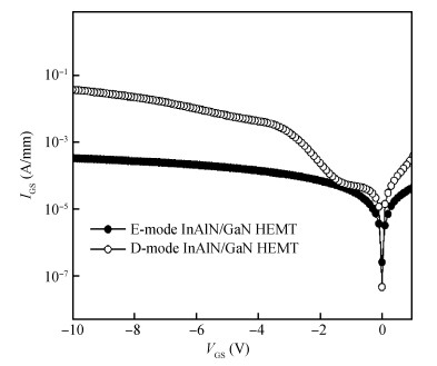
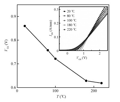
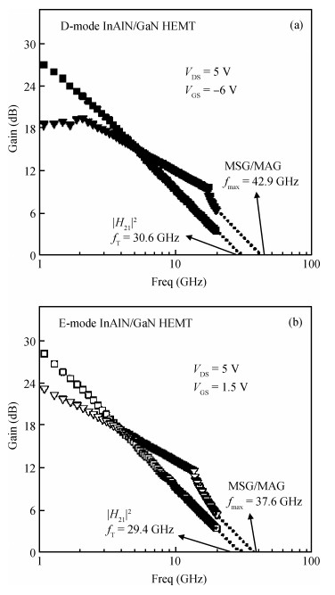
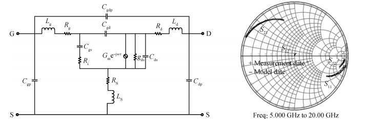
We report an enhancement-mode InAlN/GaN HEMT using a fluorine plasma treatment. The threshold voltage was measured to be +0.86 V by linear extrapolation from the transfer characteristics. The transconductance is 0 mS/mm at VGS=0 V and VDS=5 V, which shows a truly normal-off state. The gate leakage current density of the enhancement-mode device shows two orders of magnitude lower than that of the depletion-mode device. The transfer characteristics of the E-mode InAlN/GaN HEMT at room temperature and high temperature are reported. The current gain cut-off frequency (fT) and the maximum oscillation frequency (fmax) of the enhancement-mode device with a gate length of 0.3 μm were 29.4 GHz and 37.6 GHz respectively, which is comparable with the depletion-mode device. A classical 16 elements small-signal model was deduced to describe the parasitic and the intrinsic parameters of the device.

J. Semicond.
2014, 35(4): 044003 doi: 10.1088/1674-4926/35/4/044003
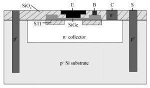
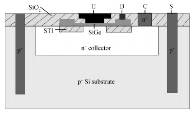
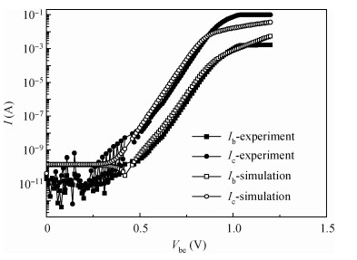
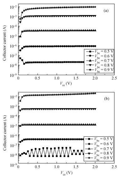
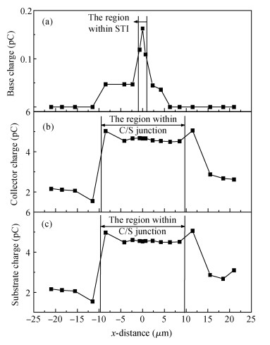
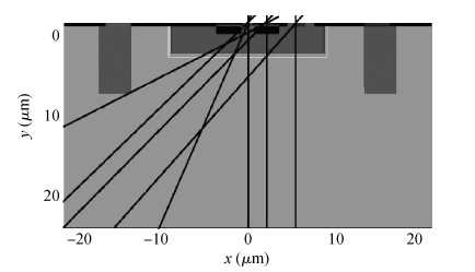
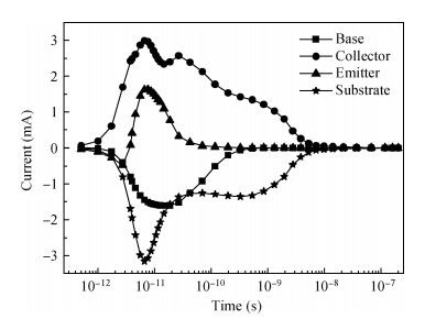
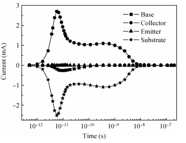
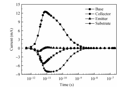
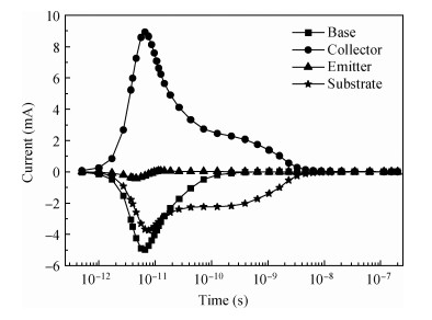
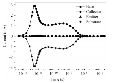
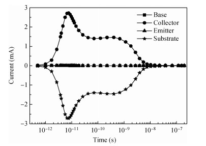
This paper presents 3-D simulation of angled strike heavy-ion induced charge collection in domestic silicon-germanium heterojunction bipolar transistors (SiGe HBTs). 3D damaged model of SiGe HBTs single-event effects (SEE) is built by TCAD simulation tools to research ions angled strike dependence. We select several different strike angles at variously typical ions strike positions. The charge collection mechanism for each terminal is identified based on analysis of the device structure and simulation results. Charge collection induced by angled strike ions presents a complex situation. Whether the location of device ions enters, as long as ions track through the sensitive volume, it will cause vast charge collection. The amount of charge collection of SiGe HBT is not only related to length of ions track in sensitive volume, but also influenced by STI and distance between ions track and electrodes. The simulation model is useful to research the practical applications of SiGe HBTs in space, and provides a theoretical basis for the further radiation hardening.


J. Semicond.
2014, 35(4): 044004 doi: 10.1088/1674-4926/35/4/044004
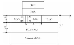
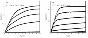
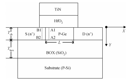
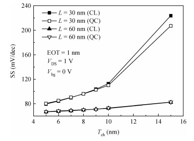
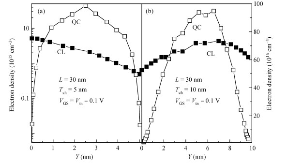
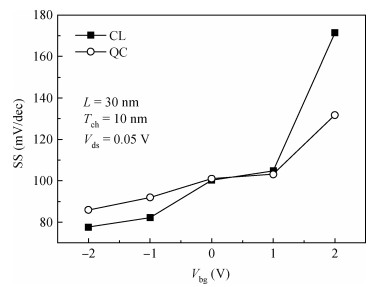
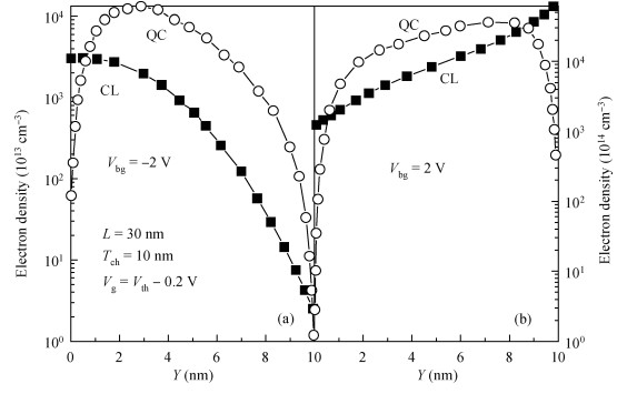
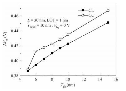
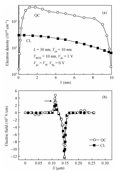
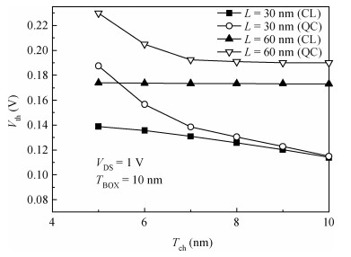
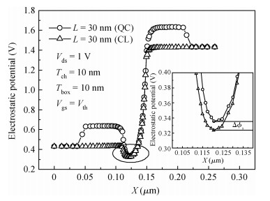
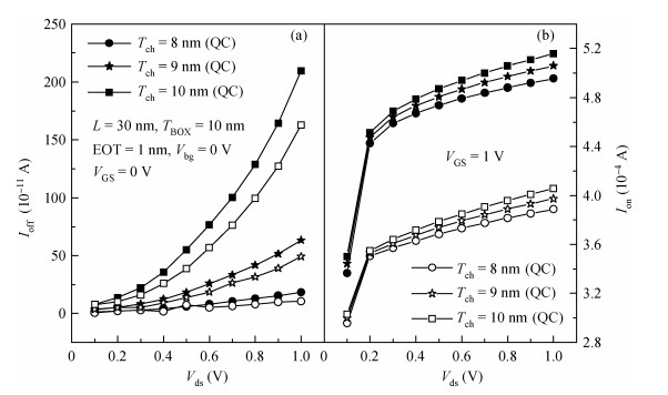
The impact of quantum confinement on the electrical characteristics of ultrathin-channel GeOI n-MOSFETs is investigated on the basis of the density-gradient model in TCAD software. The effects of the channel thickness (Tch) and back-gate bias (Vbg) on the electrical characteristics of GeOI MOSFETs are examined, and the simulated results are compared with those using the conventional semi-classical model. It is shown that when Tch > 8 nm, the electron conduction path of the GeOI MOSFET is closer to the front-gate interface under the QC model than under the CL model, and vice versa when Tch < 8 nm. Thus the electrically controlled ability of the front gate of the devices is influenced by the quantum effect. In addition, the quantum-mechanical mechanism will enhance the drain-induced barrier lowering effect, increase the threshold voltage and decrease the on-state current; for a short channel length (≤ 30 nm), when Tch > 8 nm(or < 8 nm), the quantum-mechanical mechanism mainly impacts the subthreshold slope (or the threshold voltage). Due to the quantum-size effect, the off-state current can be suppressed as the channel thickness decreases.
J. Semicond.
2014, 35(4): 044005 doi: 10.1088/1674-4926/35/4/044005
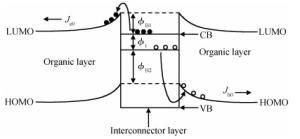
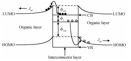
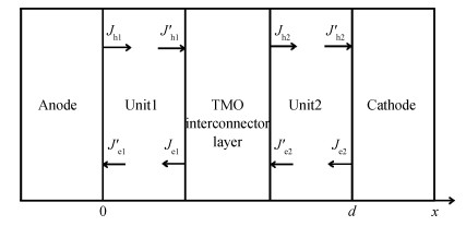
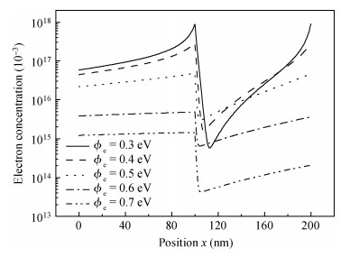
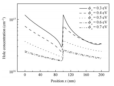
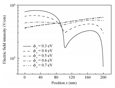
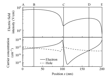
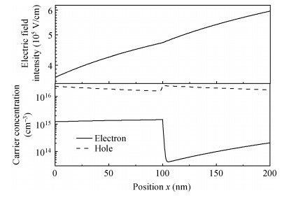
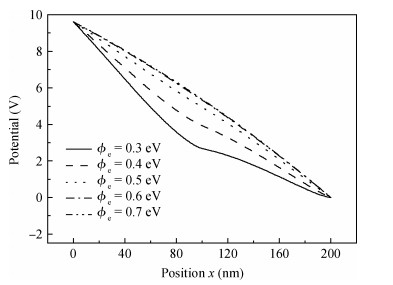
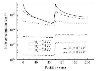
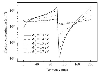
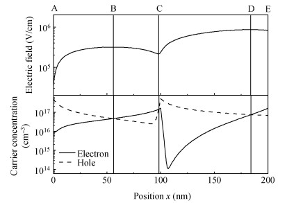
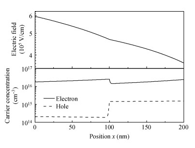
By utilizing a two-step process to express the charge generation and separation mechanism of the transition metal oxides (TMOs) interconnector layer, a numerical model was proposed for tandem organic light emitting diodes (OLEDs) with a TMOs thin film as the interconnector layer. This model is valid not only for an n-type TMOs interconnector layer, but also for a p-type TMOs interconnector layer. Based on this model, the influences of different carrier injection barriers at the interface of the electrode/organic layer on the charge generation ability of interconnector layers were studied. In addition, the distribution characteristics of carrier concentration, electric field intensity and potential in the device under different carrier injection barriers were studied. The results show that when keeping one carrier injection barrier as a constant while increasing another carrier injection barrier, carriers injected into the device were gradually decreased, the carrier generation ability of the interconnector layer was gradually reduced, the electric field intensity at the interface of the organic/electrode was gradually enhanced, and the electric field distribution became nearly linear:the voltage drops in two light units gradually became the same. Meanwhile, the carrier injection ability decreased as another carrier injection barrier increased. The simulation results agree with the experimental data. The obtained results can provide us with a deep understanding of the work mechanism of TMOs-based tandem OLEDs.


J. Semicond.
2014, 35(4): 044006 doi: 10.1088/1674-4926/35/4/044006

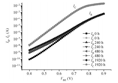
NPN-type small and medium power switching transistors in 3DK series are used to conduct analyses and studies of accelerating degradation. Through three group studies of accelerating degradation in different temperature-humidity constant stresses, the failure sensitive parameters of transistors are identified and the lifetime of samples is extrapolated from the performance degradation data. Average lifetimes in three common distributions are given, when, combined with the Hallberg-Peck temperature-humidity model, the storage lifetime of transistor samples in the natural storage condition is extrapolated between 105-107 h. According to its definition, the accelerating factor is 1462 in 100℃/100% relative humidity (RH) stress condition, and 25℃/25% RH stress condition. Finally, the degradation causes of performance parameters of the test samples are analyzed. The findings can provide certain references for the storage reliability of domestic transistors.
J. Semicond.
2014, 35(4): 044007 doi: 10.1088/1674-4926/35/4/044007

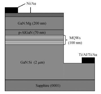
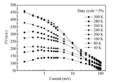
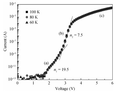
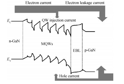
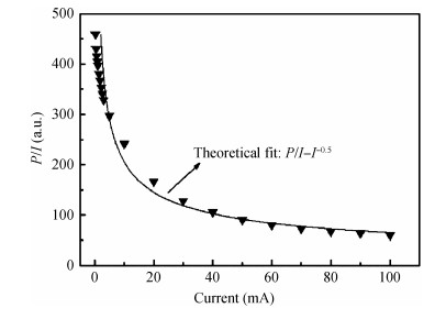
The typical light emission efficiency behaviors of InGaN/GaN multi-quantum well (MQW) blue light-emitting diodes (LEDs) grown on c-plane sapphire substrates are characterized by pulsed current operation mode in the temperature range 40 to 300 K. At temperatures lower than 80 K, the emission efficiency of the LEDs decreases approximately as an inverse square root relationship with drive current. We use an electron leakage model to explain such efficiency droop behavior; that is, the excess electron leakage into the p-side of the LEDs under high forward bias will significantly reduce the injection possibility of holes into the active layer, which in turn leads to a rapid reduction in the radiative recombination efficiency in the MQWs. Combining the electron leakage model and the quasi-neutrality principle in the p-type region, we can readily derive the inverse square root dependent function between the light emission efficiency and the drive current. It appears that the excess electron leakage into the p-type side of the LEDs is primarily responsible for the low-temperature efficiency droop behavior.
J. Semicond.
2014, 35(4): 044008 doi: 10.1088/1674-4926/35/4/044008
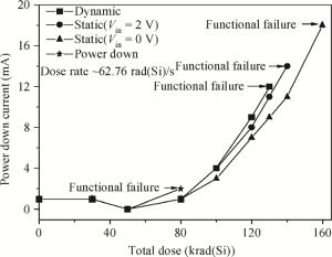
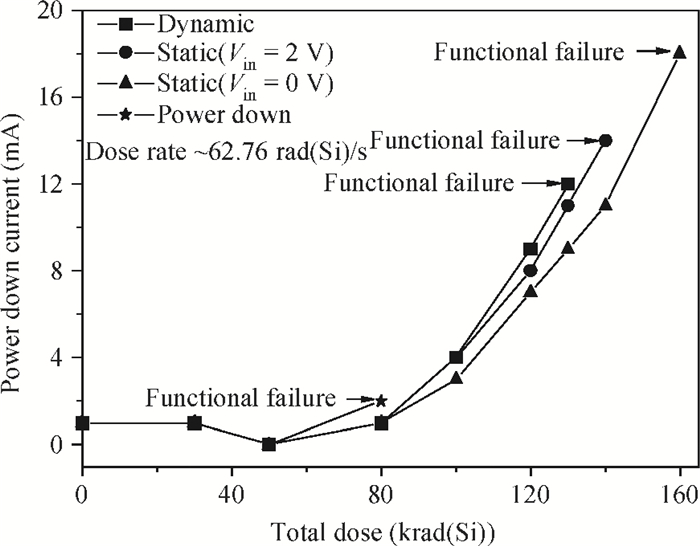
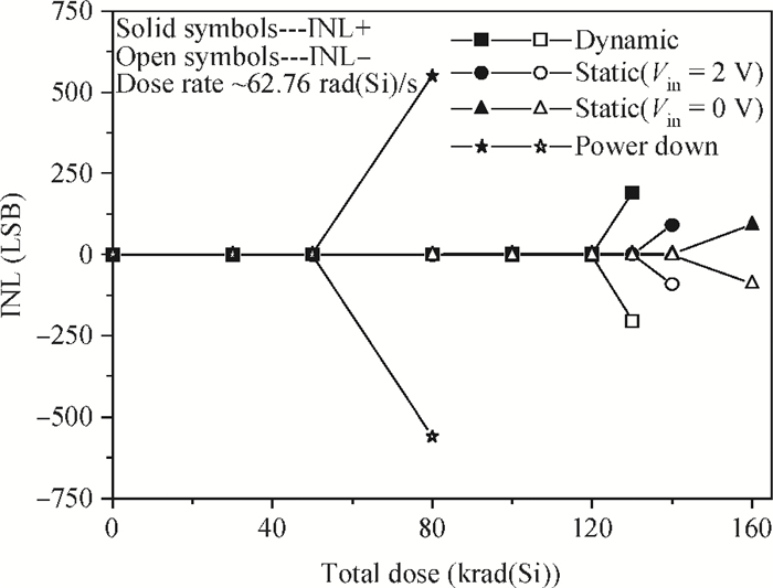
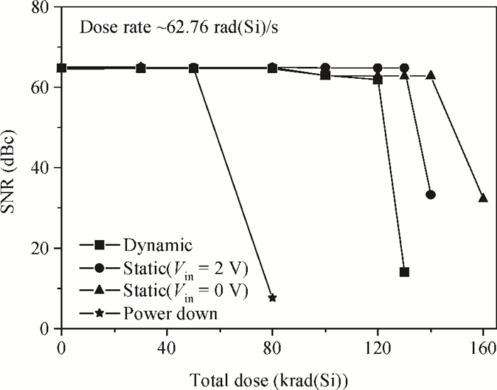
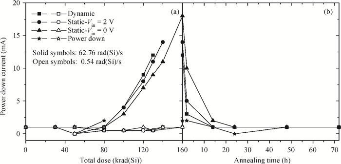
This paper presents the total ionizing dose test results at different biases and dose rates for AD9233, which is fabricated using a modern CMOS process. The experimental results show that the digital parts are more sensitive than the other parts. Power down is the worst-case bias, and this phenomenon is first found in the total ionizing dose effect of analog-to-digital converters. We also find that the AC as well as DC parameters are sensitive to the total ionizing dose at a high dose rate, whereas none of the parameters are sensitive at a low dose rate. The test facilities, results and analysis are presented in detail.
J. Semicond.
2014, 35(4): 045001 doi: 10.1088/1674-4926/35/4/045001
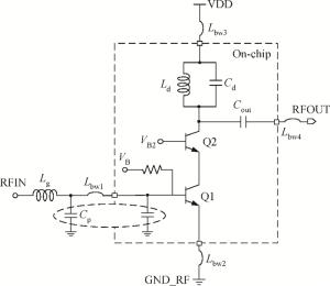
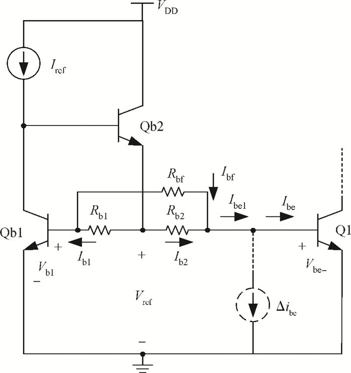
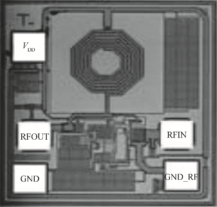
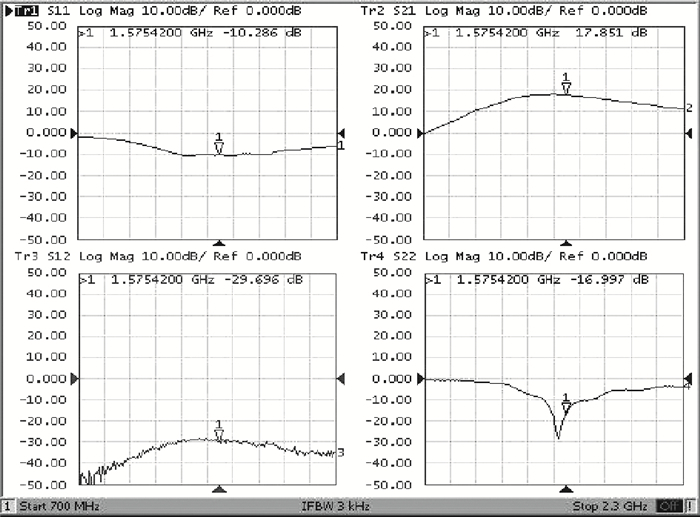
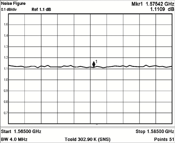
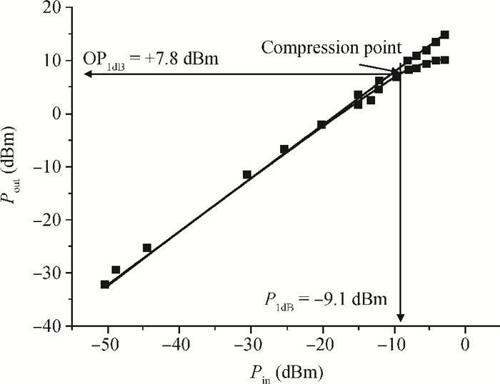
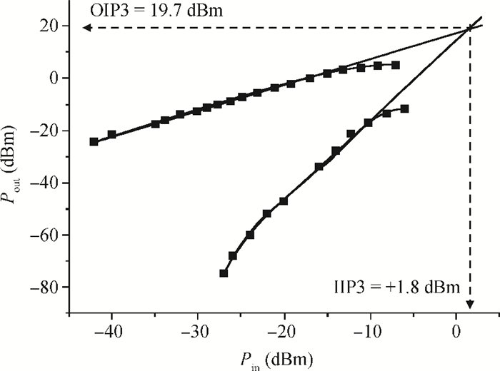
A high linearity 1.575 GHz SiGe:HBT low noise amplifier (LNA) for global positioning system applications is described. The bipolar cascoded with an MOSFET LNA was fabricated in a commercial 0.18 μm SiGe BiCMOS process. A resistor bias feed circuit with a feedback resistor was designed for the LNA input transistor to improve its intermodulation and compression performance. The packaged chip tested on board has displayed a noise figure of 1.11 dB, a power gain of 18 dB, an output 1 dB compression point of +7.8 dBm and an input third-order intercept point of +1.8 dBm. The chip occupies a 500×560 μm2 area and consumes 3.6 mA from a 2.85 V power supply.


J. Semicond.
2014, 35(4): 045002 doi: 10.1088/1674-4926/35/4/045002
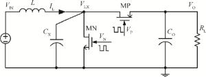
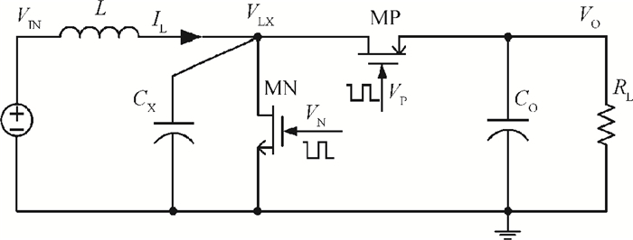
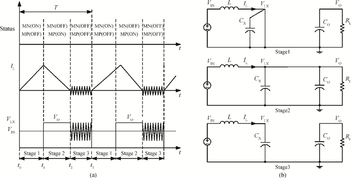
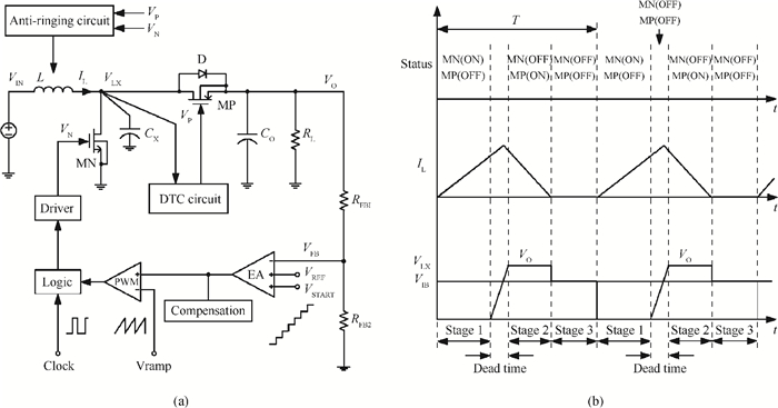
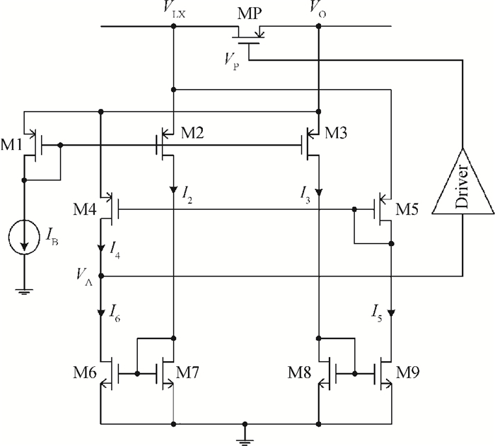
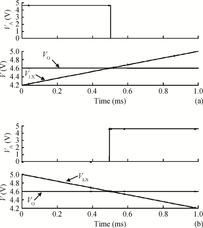
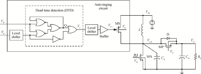
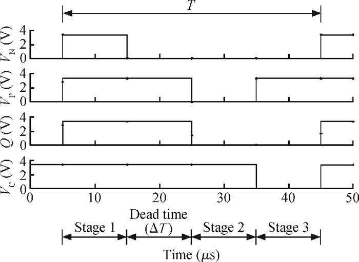
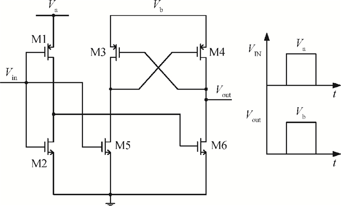
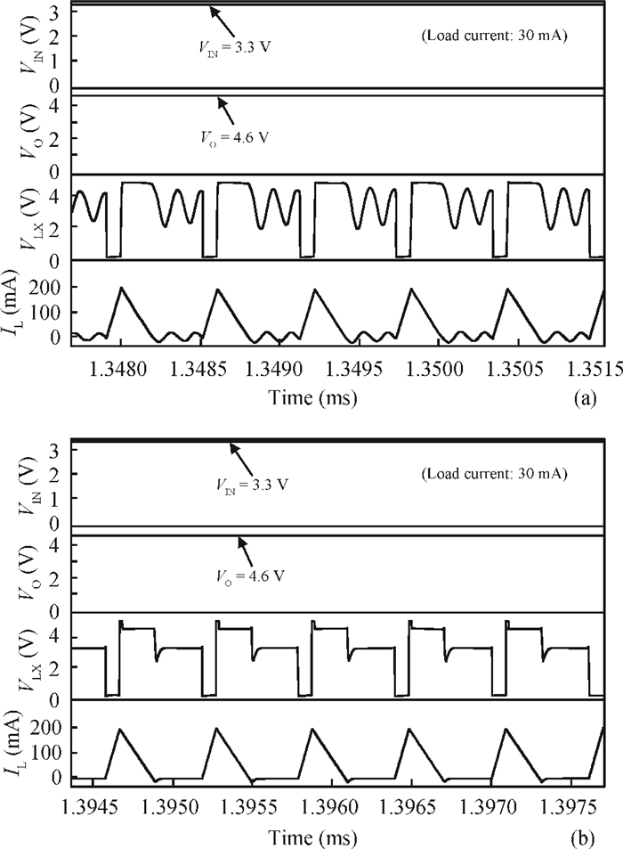
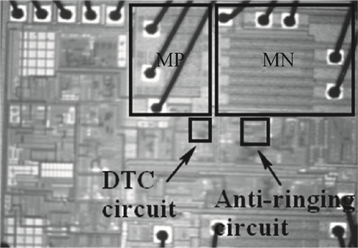
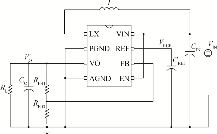
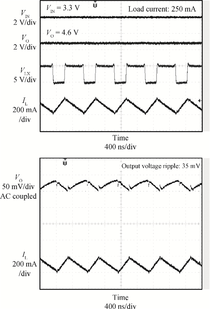
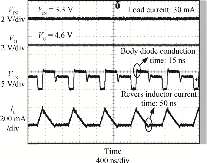
A synchronous boost DC-DC converter with an adaptive dead time control (DTC) circuit and anti-ringing circuit is presented. The DTC circuit is used to provide adjustable dead time and zero inductor current detection for power transistors and therefore, a high efficiency is achieved by minimizing power losses, such as the shoot-through current loss, the body diode conduction loss, the charge-sharing loss and the reverse inductor current loss. Simultaneously, a novel anti-ringing circuit controlled by the switching sequence of power transistors is developed to suppress the ringing when the converter enters the discontinuous conduction mode (DCM) for low electromagnetic interference (EMI) and additional power savings. The proposed converter has been fabricated in a 0.6 μm CDMOS technology. Simulation and experimental results show that the power efficiency of the boost converter is above 81% under different load currents from 10 to 250 mA and a peak efficiency of 90% is achieved at about 100 mA. Moreover, the ringing is easily suppressed by the anti-ringing circuit and therefore the EMI noise is attenuated.


J. Semicond.
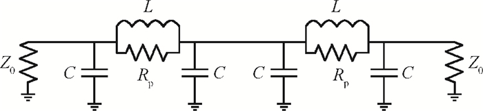
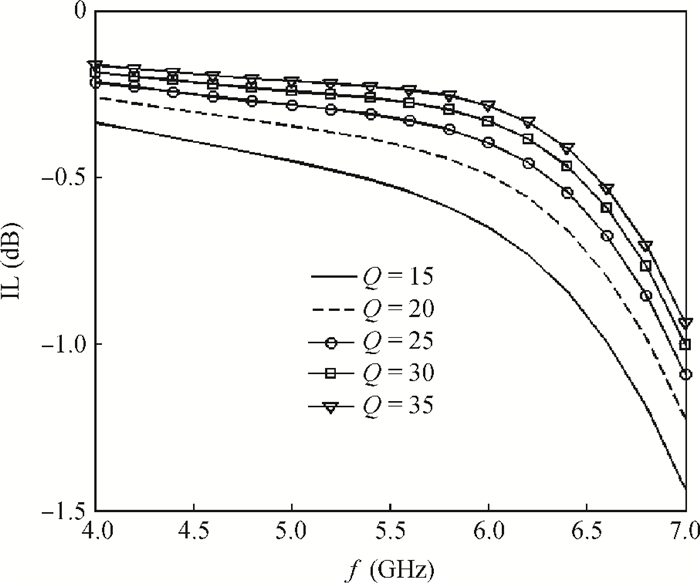
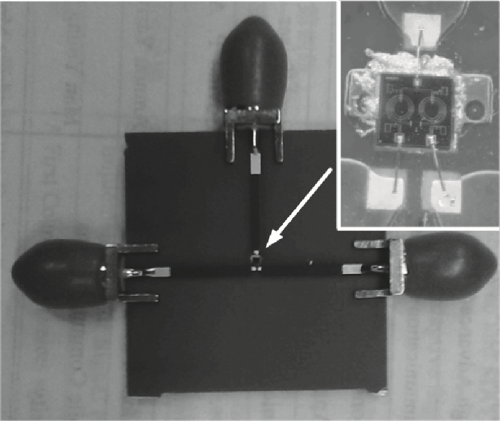
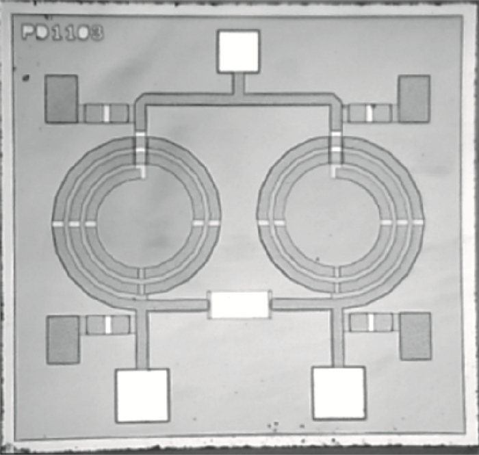
2014, 35(4): 045003 doi: 10.1088/1674-4926/35/4/045003
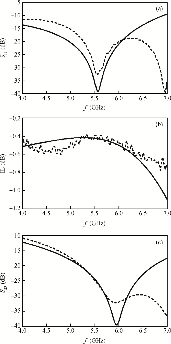
A compact lumped integrated power divider with low insertion loss using 0.5 μm GaAs pHEMT technology is presented. The proposed power divider uses the π-type LC network for transmission line equivalence and a thin film resistor for isolation tuning simultaneously. The quality factor of the inductor is analyzed and synthesized for insertion-loss influence. The measured insertion loss is less than 0.5 dB when the operating frequency is within the range of 5.15-6.15 GHz. The return loss and isolation are better than 15 dB and 20 dB, respectively. The compact dimension of the power divider is as small as 0.9×0.85 mm2. The measured results agree well with the simulated ones.
J. Semicond.
2014, 35(4): 045004 doi: 10.1088/1674-4926/35/4/045004

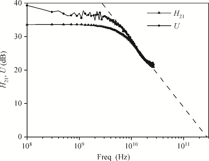
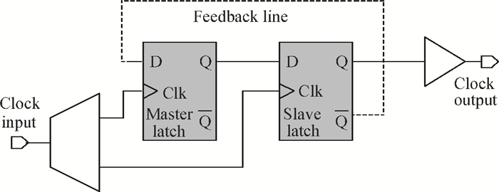
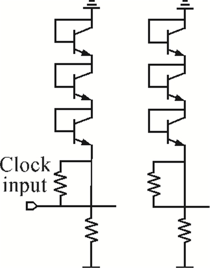
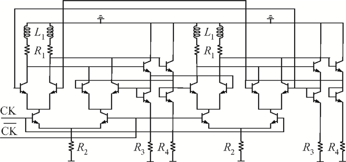
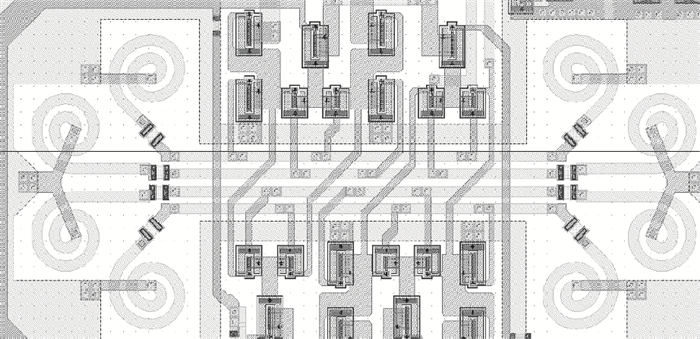
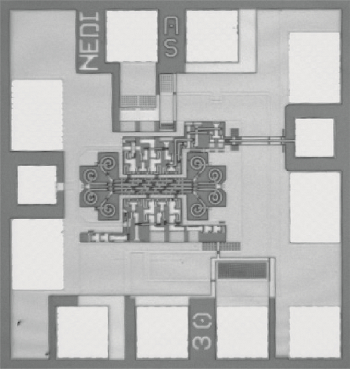
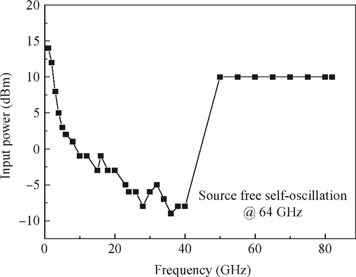
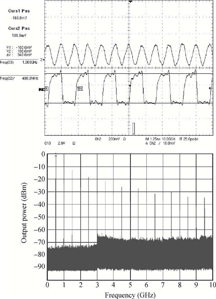
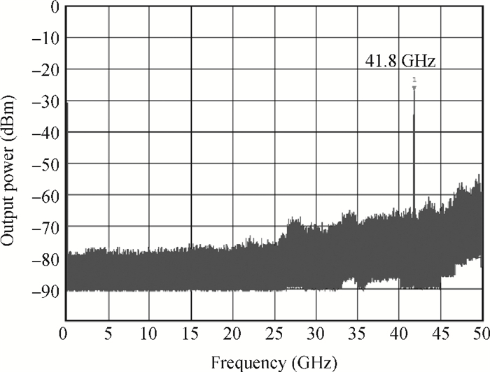
A static frequency divider is presented using 0.7 μm InP DHBTs with 280 GHz 1ft/fmax. The divider is based on ECL master-slave D-flip-flop topology with 30 HBTs and 20 resistors with a chip size 0.62×0.65 mm2. The circuits use peaking inductance as a part of the loads to maximize the highest clock rate. Momentum simulation is used to accurately characterize the effect of the clock feedback lines at the W band. Test results show that the divider can operate from 1 GHz up to 83 GHz. Its phase noise is 139 dBc/Hz with 100 kHz offset. The power dissipation of divider core is 350 mW.

J. Semicond.
2014, 35(4): 045005 doi: 10.1088/1674-4926/35/4/045005

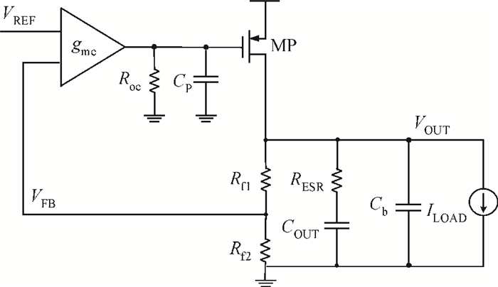
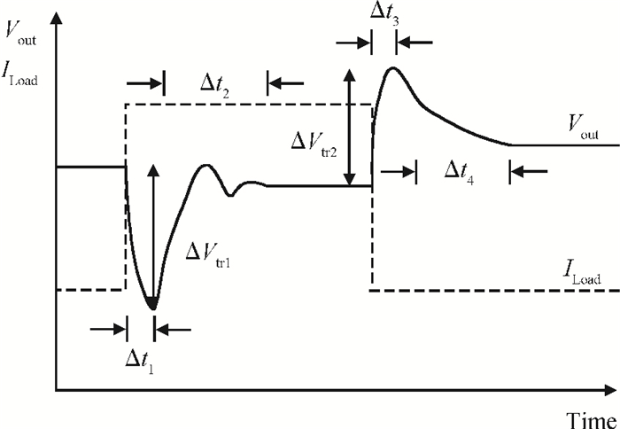
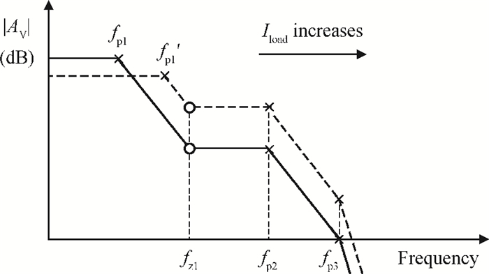
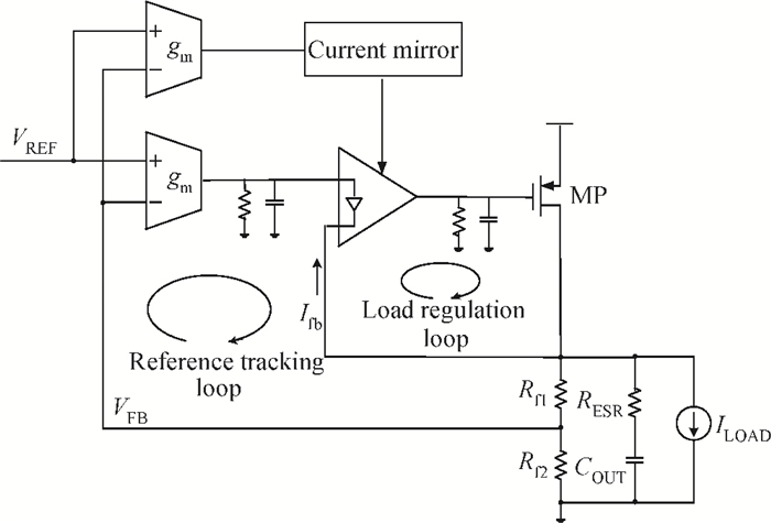
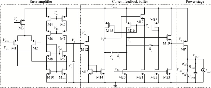
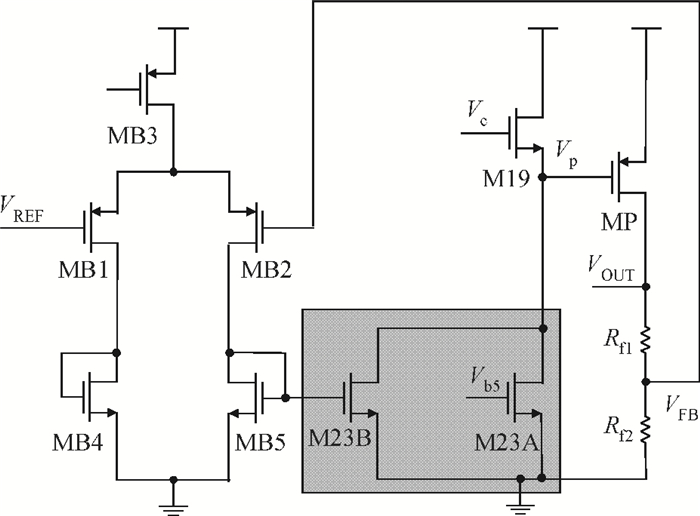
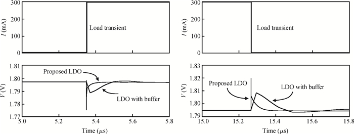
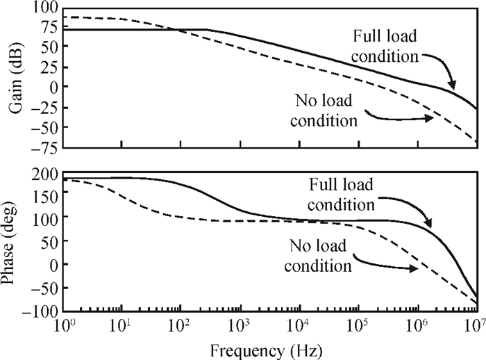
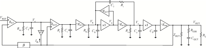
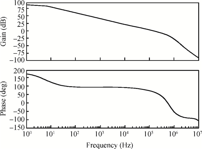
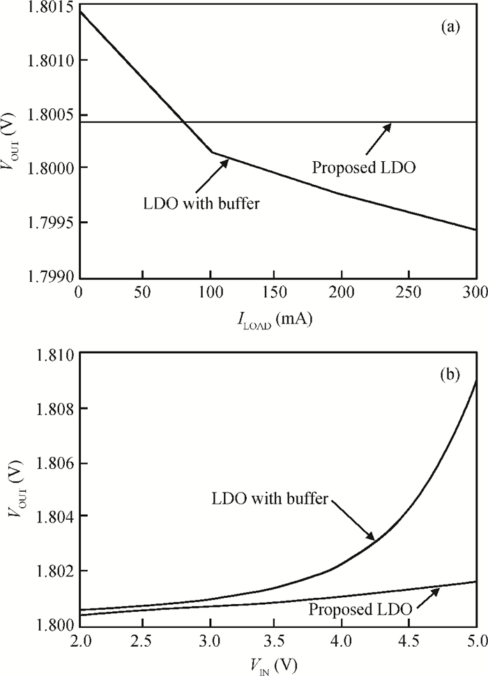
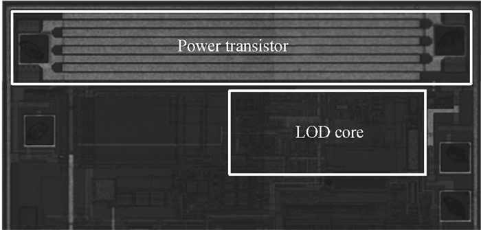
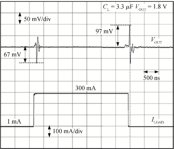
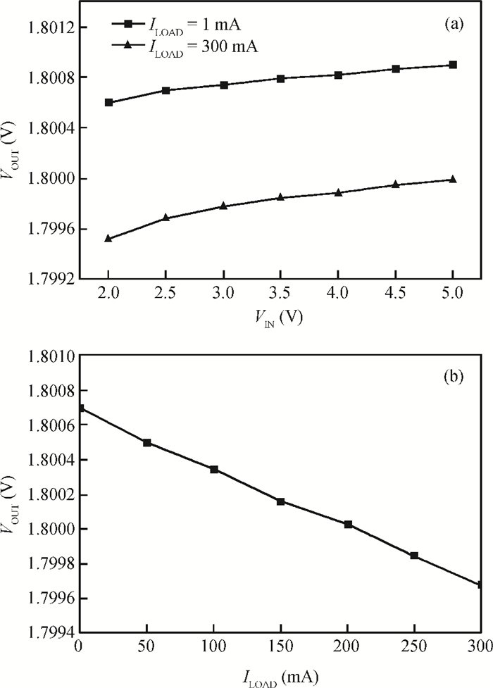
This paper presents a low-dropout regulator (LDO) for portable applications with dual-loop feedback and a dynamic bias circuit. The dual-loop feedback structure is adopted to reduce the output voltage spike and the response time of the LDO. The dynamic bias circuit enhances the slew rate at the gate of the power transistor. In addition, an adaptive miller compensation technique is employed, from which a single pole system is realized and over a 59° phase margin is achieved under the full range of the load current. The proposed LDO has been implemented in a 0.6-μm CMOS process. From the experimental results, the regulator can operate with a minimum dropout voltage of 200 mV at a maximum 300 mA load and IQ of 113 μA. The line regulation and load regulation are improved to 0.1 mV/V and 3.4 μV/mA due to the sufficient loop gain provided by the dual feedback loops. Under a full range load current step, the voltage spikes and the recovery time of the proposed LDO is reduced to 97 mV and 0.142 μs respectively.

J. Semicond.
2014, 35(4): 045006 doi: 10.1088/1674-4926/35/4/045006
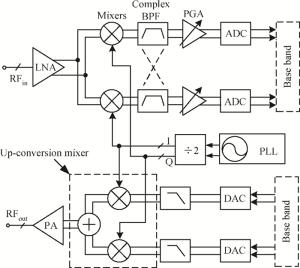
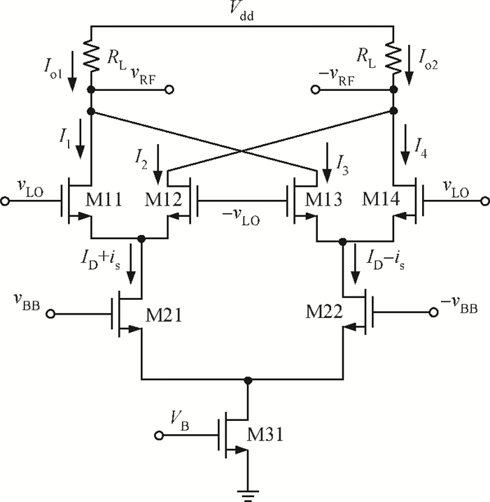
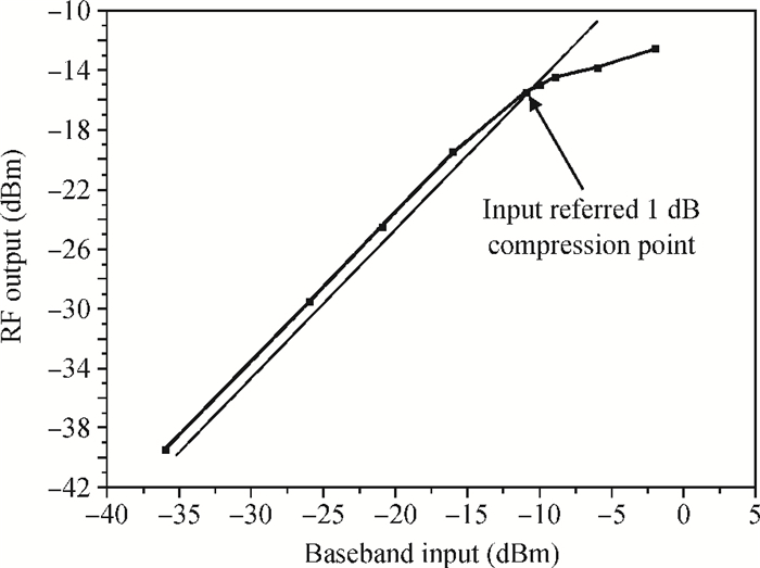
This paper presents an up-conversion mixer for 2.4-2.4835 GHz wireless sensor networks (WSN) in 0.18 μm RF CMOS technology. It was based on a double-balanced Gilbert cell type, with two Gilbert cells having quadrature modulation applied. Current-reuse and cross positive feedback techniques were applied in the mixer to boost conversion gain; the current source stage was removed from the mixer to improve linearity. Measured results exhibited that under a 1 V power supply, the conversion gain was 5 dB, the input referred 1 dB compression point was -11 dBm and the ⅡP3 was -0.75 dBm, while it only consumed 1.4 mW.


J. Semicond.
2014, 35(4): 045007 doi: 10.1088/1674-4926/35/4/045007

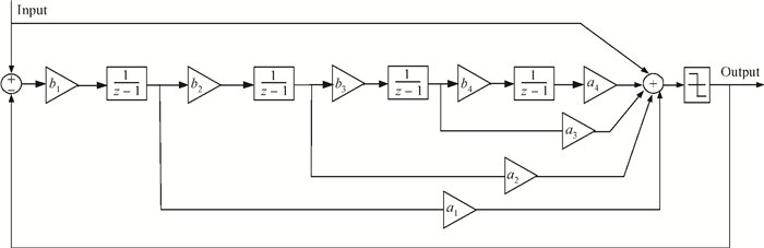
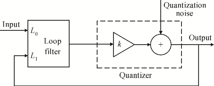
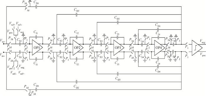
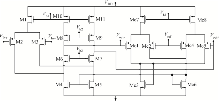
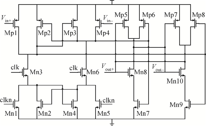
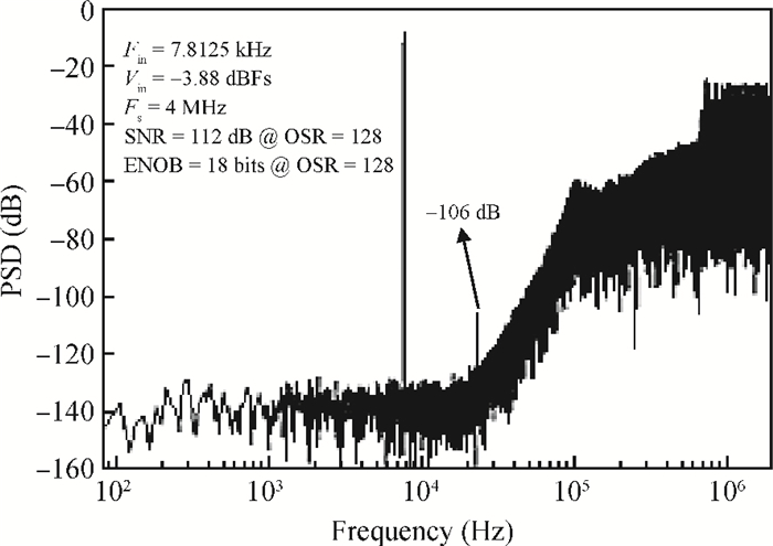
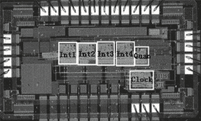
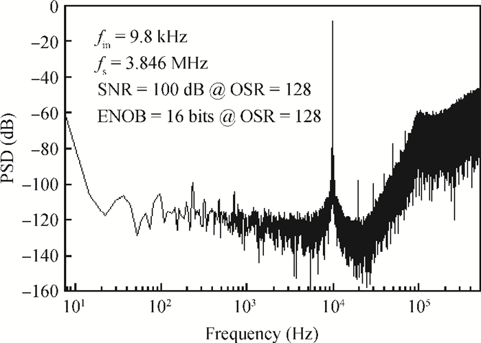
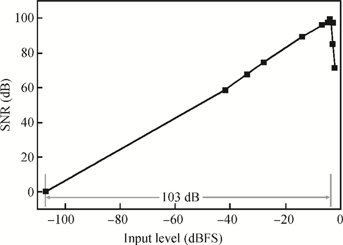
A fourth-order low-distortion low-pass sigma-delta (Σ Δ) modulator is presented for micro-machined inertial sensors. The proposed single-loop single-bit feedback modulator is optimized with a feed-forward path to decrease the nonlinearities and power consumption. The IC is implemented in a standard 0.6 μm CMOS technology and operates at a sampling frequency of 3.846 MHz. The chip area is 2.12 mm2 with 23 pads. The experimental results indicate a signal-to-noise ratio (SNR) of 100 dB and dynamic range (DR) of 103 dB at an oversampling rate (OSR) of 128 with the input signal amplitude of -3.88 dBFS at 9.8 kHz; the power consumption is 15 mW at a 5 V supply.
J. Semicond.
2014, 35(4): 045008 doi: 10.1088/1674-4926/35/4/045008
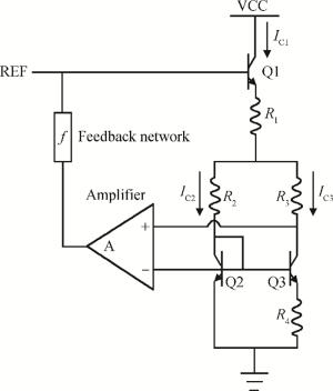
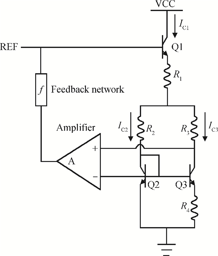
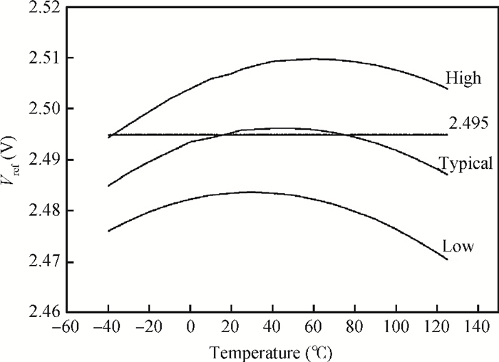
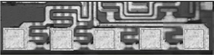
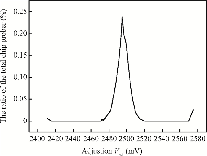
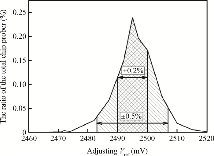
To design a high-precision reference, the various error sources have been analyzed and compensated with a compact 111 mV resistor-trim scheme and the upper and lower extremes of the reference precision are also temperature-compensated. At room temperature, the yield of ±0.5% precision is 96% and ±0.2% is 78%.

J. Semicond.
2014, 35(4): 045009 doi: 10.1088/1674-4926/35/4/045009
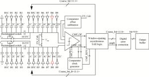
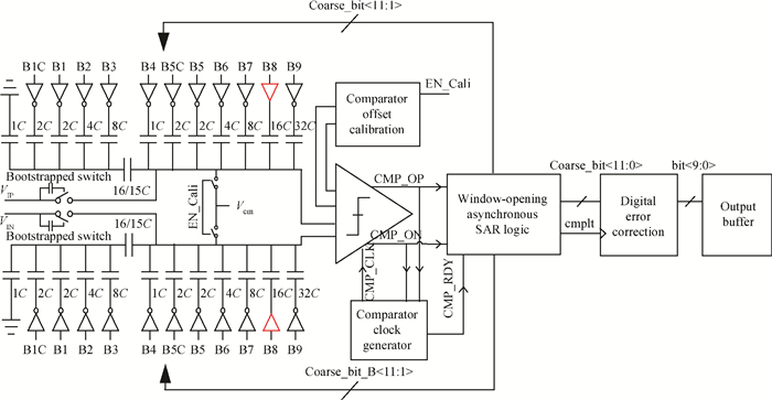
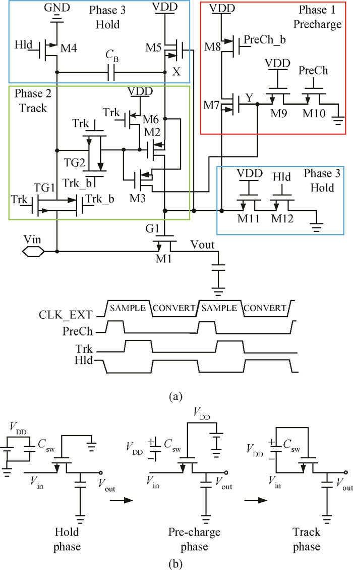
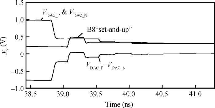
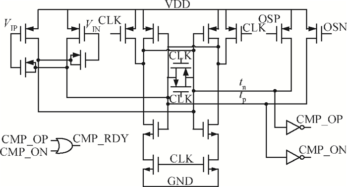
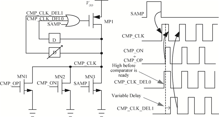
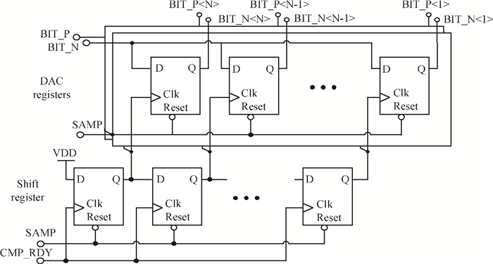
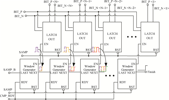
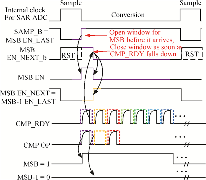
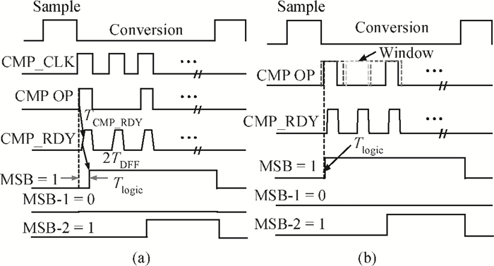
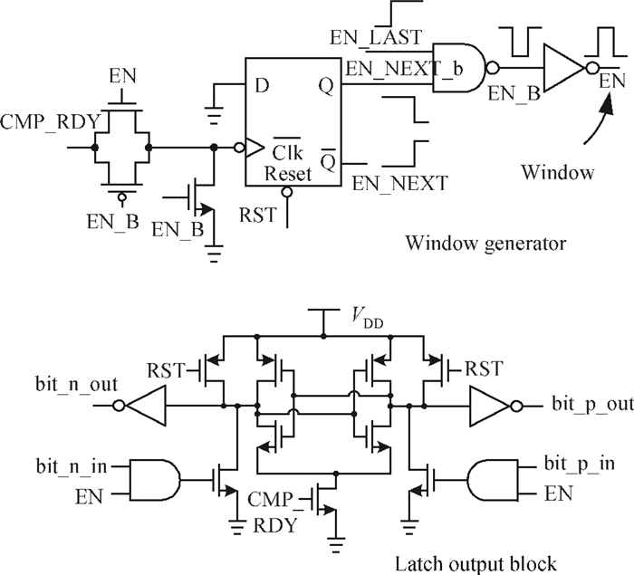
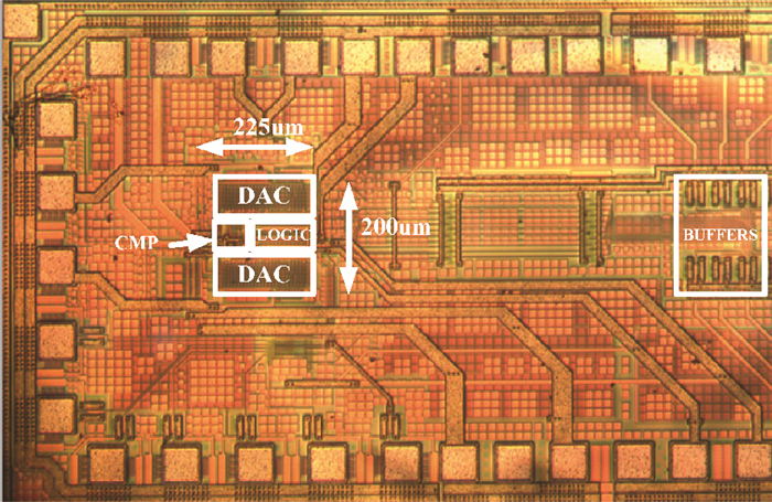
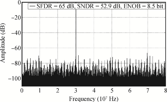
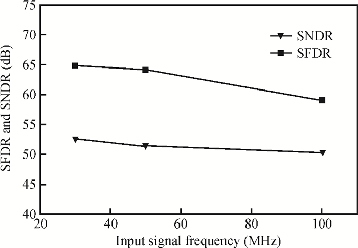
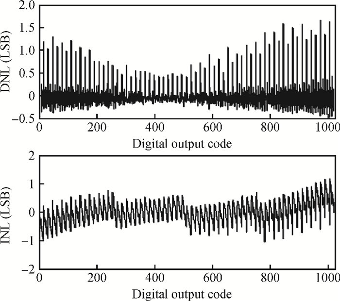
This paper demonstrates a single-channel 10-bit 160 MS/s successive-approximation-register (SAR) analog-to-digital converter (ADC) in 65 nm CMOS process with a 1.2 V supply voltage. To achieve high speed, a new window-opening logic based on the asynchronous SAR algorithm is proposed to minimize the logic delay, and a partial set-and-down DAC with binary redundancy bits is presented to reduce the dynamic comparator offset and accelerate the DAC settling. Besides, a new bootstrapped switch with a pre-charge phase is adopted in the track and hold circuits to increase speed and reduce area. The presented ADC achieves 52.9 dB signal-to-noise distortion ratio and 65 dB spurious-free dynamic range measured with a 30 MHz input signal at 160 MHz clock. The power consumption is 9.5 mW and a core die area of 250×200 μm2 is occupied.
J. Semicond.
2014, 35(4): 045010 doi: 10.1088/1674-4926/35/4/045010

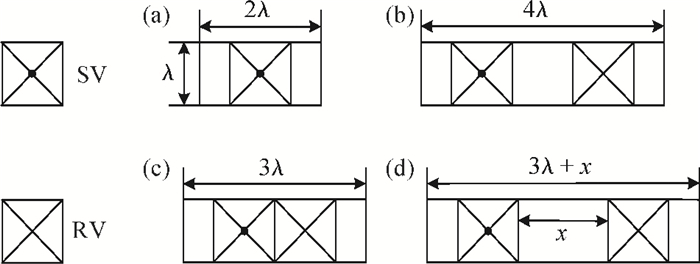
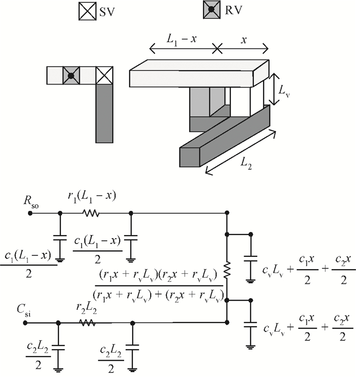
Redundant via (RV) insertion is a useful mechanism to enhance via reliability. However, when extra vias are inserted into the design, the circuit timing might be changed. Therefore, how to insert RV under the timing constraints is the main challenge. In this paper, we introduce a new model to compute the distance between a RV and the corresponding single via, put forward a new RV type, which is called the long length via (LLV), and then present an improved RV insertion method considering the timing constraints. This computing model can certify that the timing, which is obtained after inserting a RV, is not greater than the original timing. Meanwhile, the new RV type LLV can increase the possibility of RV insertion; this method provides a global perspective for the RV insertion. Considering the timing constraints, the total redundant via insertion rate is 85.38% in the MIS-based method, while our proposed method can obtain a high insertion rate 88.79% for the tested circuits.
J. Semicond.
2014, 35(4): 045011 doi: 10.1088/1674-4926/35/4/045011

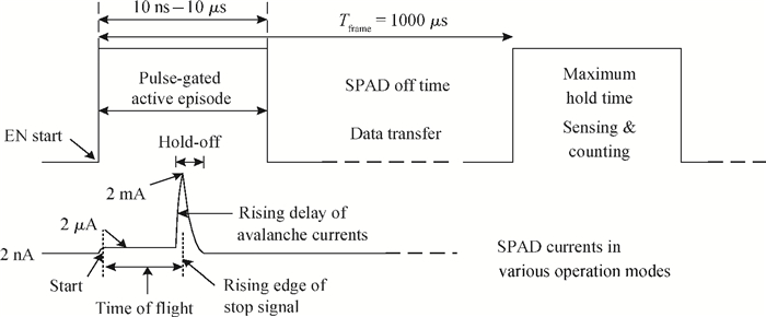
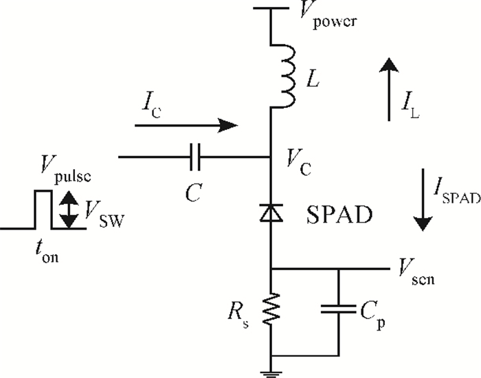
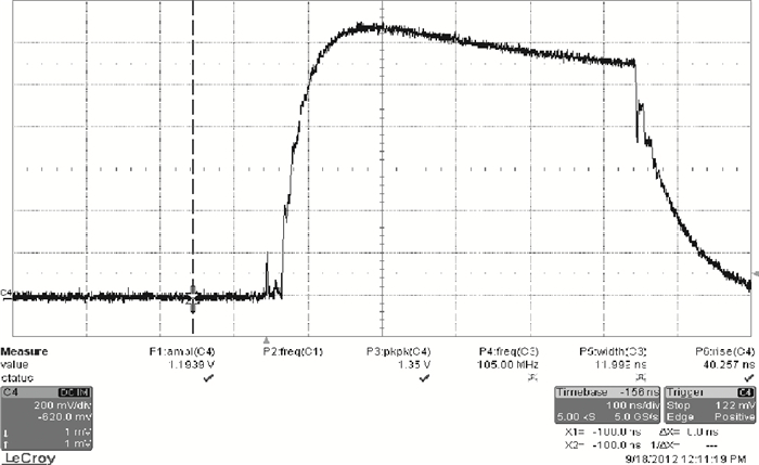
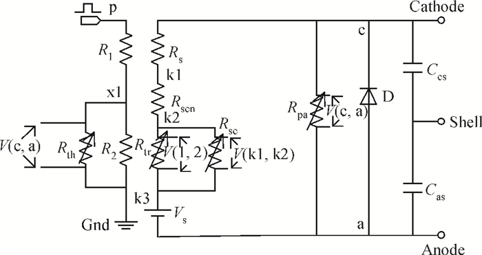
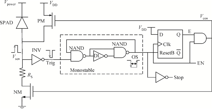
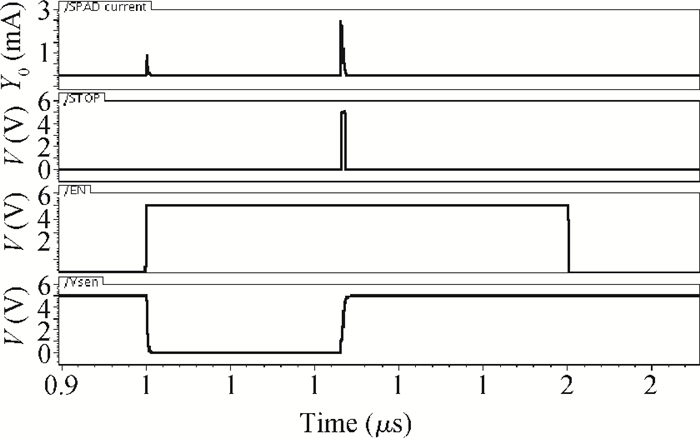
We present a novel gated operation active quenching circuit (AQC). In order to simulate the quenching circuit a complete SPICE model of a InGaAs SPAD is set up according to the I-V characteristic measurement results of the detector. The circuit integrated with a ROIC (readout integrated circuit) is fabricated in an CSMC 0.5 μm CMOS process and then hybrid packed with the detector. Chip measurement results show that the functionality of the circuit is correct and the performance is suitable for practical system applications.

J. Semicond.
2014, 35(4): 046001 doi: 10.1088/1674-4926/35/4/046001
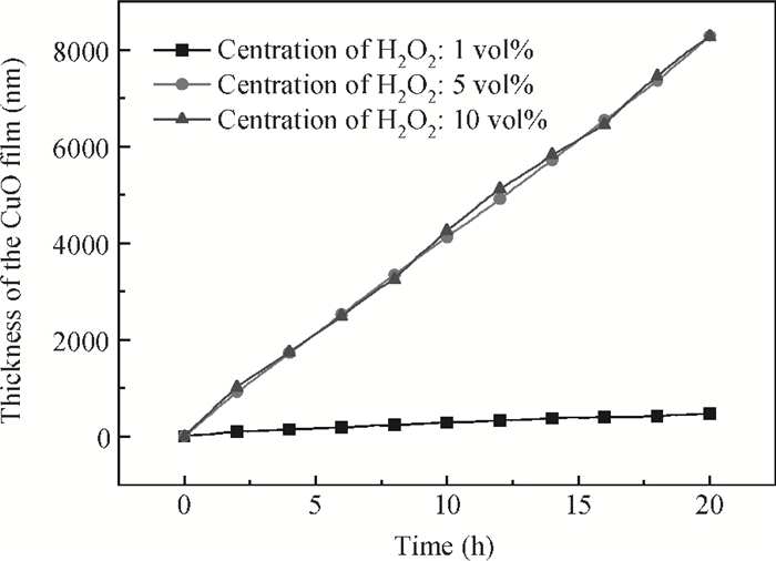
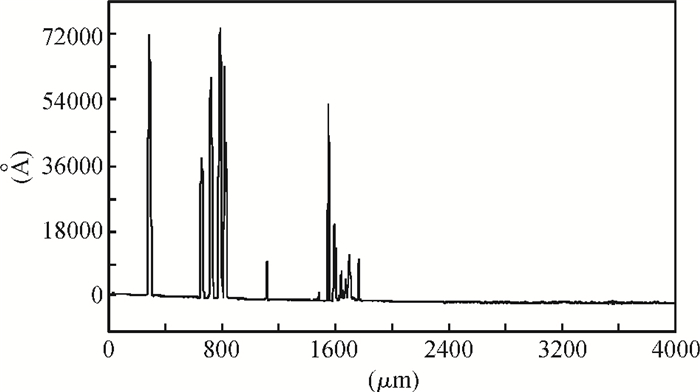
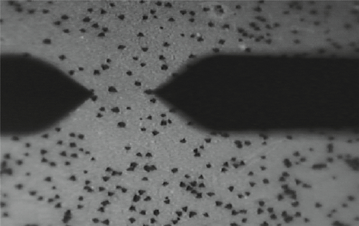
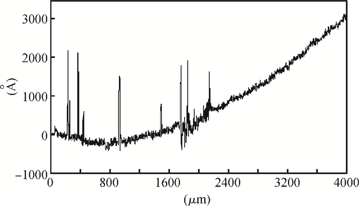
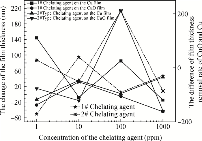
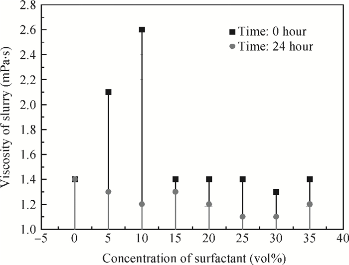
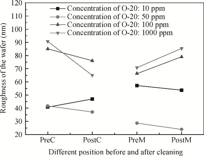
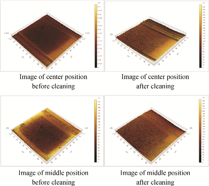
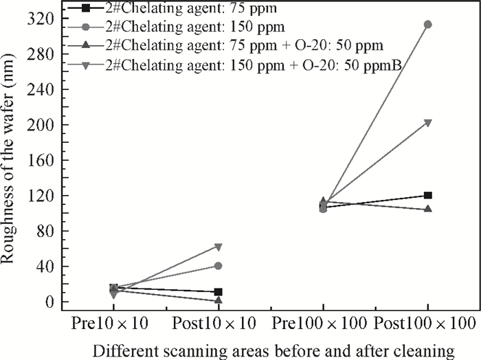
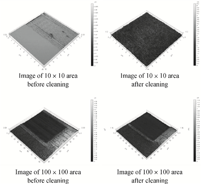
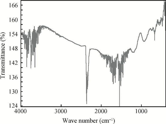
This article introduces the removal technology of CuO particles on the post CMP wafer surface of multi-layered copper. According to the Cu film corrosion curve with different concentrations of H2O2 and the effect curve of time on the growth rate of CuO film, CuO film with the thickness of 220 nm grown on Cu a surface was successfully prepared without the interference of CuCl2· 2H2O. Using the static corrosion experiment the type of chelating agent (FA/O Ⅱ type chelating agent) and the concentration range (10-100 ppm) for CuO removal was determined, and the Cu removal rate was close to zero. The effect of surfactant on the cleaning solution properties was studied, and results indicated that the surfactant has the effect of reducing the surface tension and viscosity of the cleaning solution, and making the cleaning agent more stable. The influence of different concentrations of FA/O Ⅰ type surfactant and the mixing of FA/O Ⅱ type chelating agent and FA/O Ⅰ type surfactant on the CuO removal effect and the film surface state was analyzed. The experimental results indicated that when the concentration of FA/O Ⅰ type surfactant was 50 ppm, CuO particles were quickly removed, and the surface state was obviously improved. The best removal effect of CuO on the copper wiring film surface was achieved with the cleaning agent ratio of FA/O Ⅱ type chelating agent 75 ppm and FA/O Ⅰ type surfactant 50 ppm. Finally, the organic residue on the copper pattern film after cleaning with that cleaning agent was detected, and the results showed that the cleaning used agent did not generate organic residues on the film surface, and effectively removes the organic residue on the wafer.


J. Semicond.
2014, 35(4): 046002 doi: 10.1088/1674-4926/35/4/046002
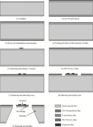
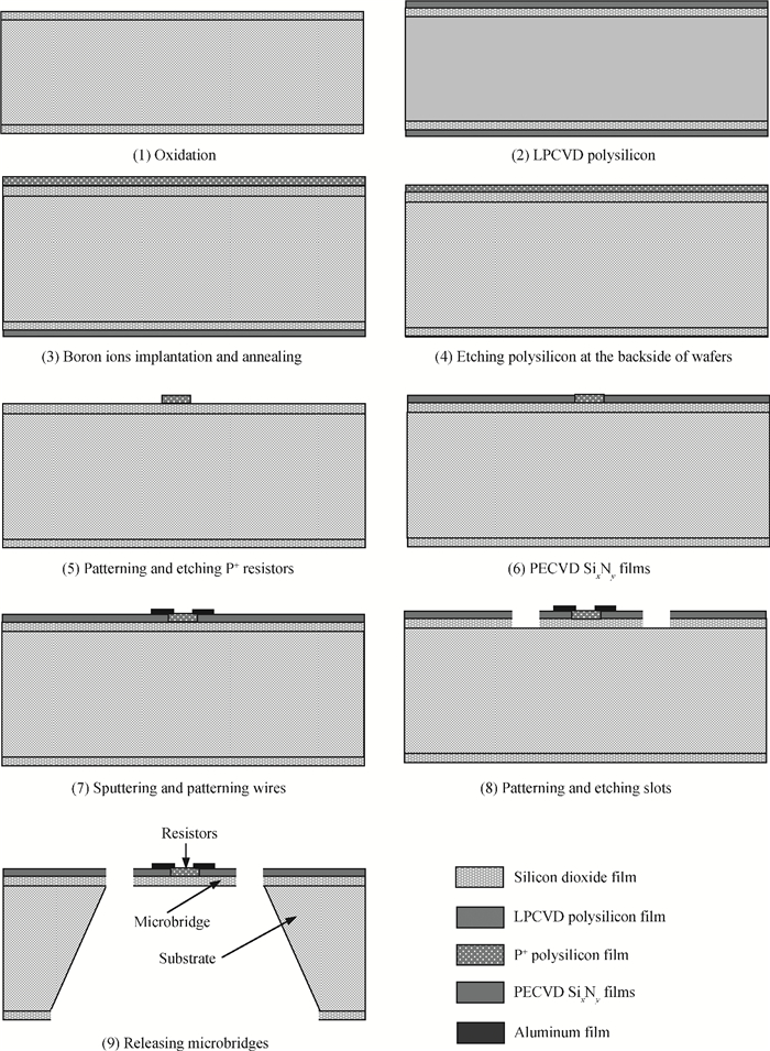
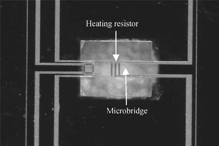
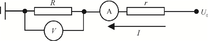
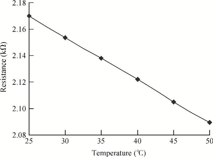
In order to balance the compressive stress of a silicon dioxide film and compose a steady MEMS structure, a silicon-rich silicon nitride film with tensile stress is deposited by plasma enhanced chemical vapor deposition process. Accurately measuring the thermal conductivity of the film is highly desirable in order to design, simulate and optimize MEMS devices. In this paper, a SiO2/SixNy bimaterial microbridge structure is presented to measure the thermal conductivity of the silicon-rich silicon nitride film by single steady-state measurement. The thermal conductivity is extracted as 3.25 W/(m· K). Low thermal conductivity indicates that the silicon-rich silicon nitride film can still be utilized as thermally insulating material in thermal sensors although its thermal conductivity is slightly larger than the values reported in literature.