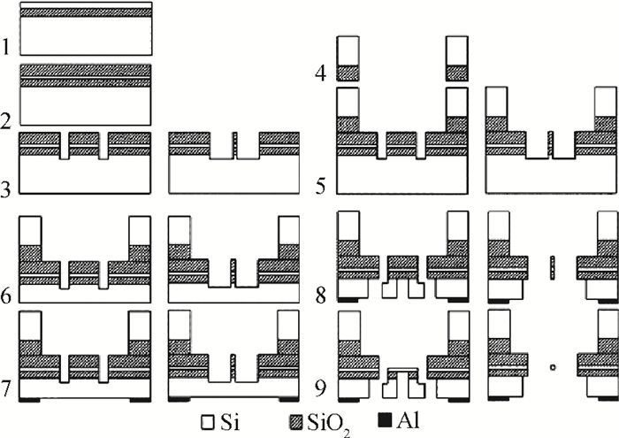
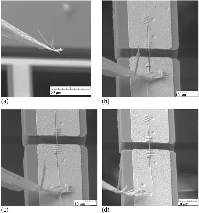
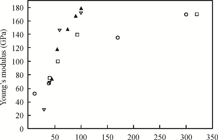
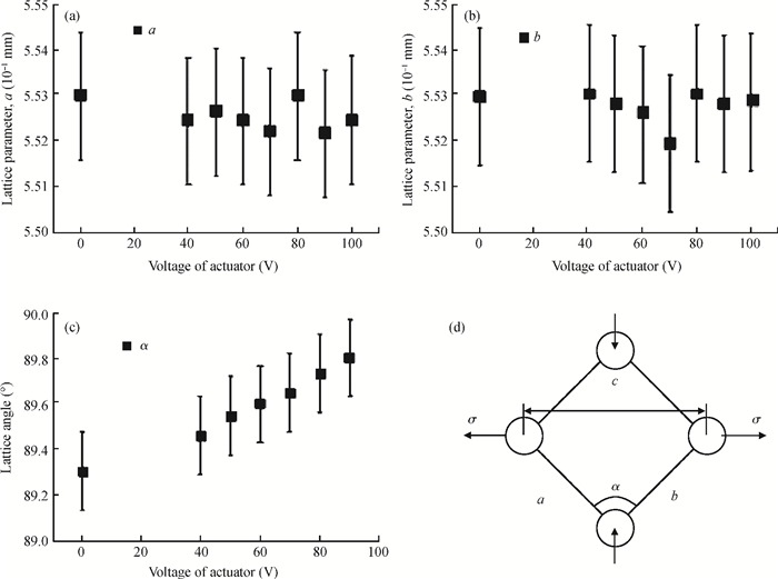
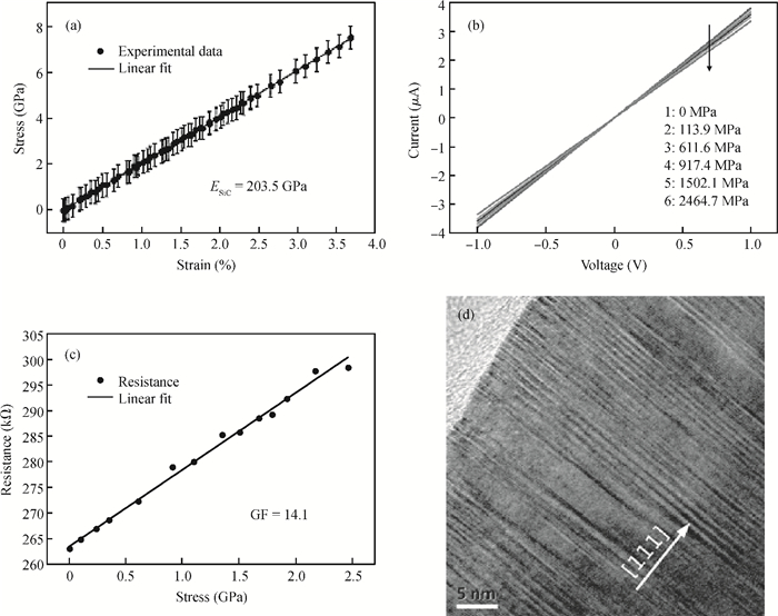
Our investigation of in situ observations on electronic and mechanical properties of nano materials using a scanning electron microscope (SEM) and a transmission electron microscope (TEM) with the help of traditional micro-electro-mechanical system (MEMS) technology has been reviewed. Thanks to the stability, continuity and controllability of the loading force from the electrostatic actuator and the sensitivity of the sensor beam, a MEMS tensile testing chip for accurate tensile testing in the nano scale is obtained. Based on the MEMS chips, the scale effect of Young's modulus in silicon has been studied and confirmed directly in a tensile experiment using a transmission electron microscope. Employing the nanomanipulation technology and FIB technology, Cu and SiC nanowires have been integrated into the tensile testing device and their mechanical, electronic properties under different stress have been achieved, simultaneously. All these will aid in better understanding the nano effects and contribute to the designation and application in nano devices.


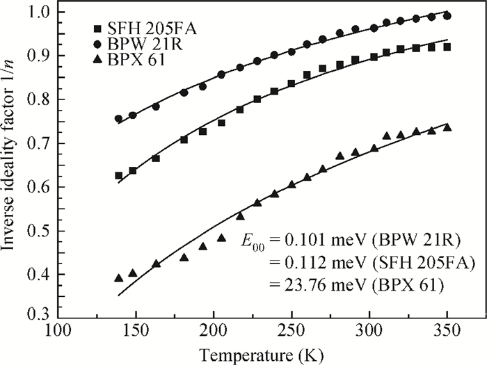
We investigate the dominant dark current transport mechanism in Si based p-i-n photodiodes, namely, BPW 21R, SFH 205FA and BPX 61 photodiodes in the temperature range of 350 to 139 K. The forward current-voltage characteristics of these photodiodes are explained via the tunneling enhanced recombination model, which gives a quantitative description of the electronic mechanism in the p-i-n junction photodiodes. The observed temperature dependence of the saturation current and the diode ideality factor of these devices agree well with theoretical predictions; the analysis also indicates the importance of doping for enhancement of tunneling. The present study will be helpful in applying the devices at low temperature ambience.


Polarons bound to a shallow Coulomb impurity center in cylindrical quantum wire is studied by a variational approach. The binding energies of the shallow impurity states in AlxGa1-xAs cylindrical quantum wire are calculated as functions of the composition x and the impurity position. It is confirmed that the binding energies are reduced obviously by the influence of the electron-phonon interaction and the binding energies are increased with increasing the composition x.


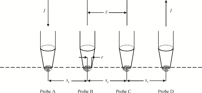
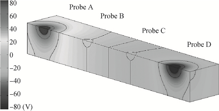
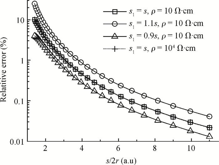
The four-probe technique is widely used in the characterization of electrical properties of solids and thin films. To investigate the influence of finite size probes with non-planar contact on the standard four-probe method, we have proposed an image method to simulate the potential distribution within the specimen. The numerical results show that for infinitely thick samples, the standard method can only provide accurate determination of resistivity (relative error below 1%) when the ratio of the average inter-electrode spacing to the diameter of the probe is greater than 3. We have also found that disregarding the probe size brings a less dominate error than that introduced by the approximate formula, when the sample's thickness is close to the inter-electrode spacing.

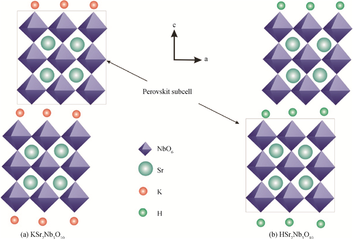
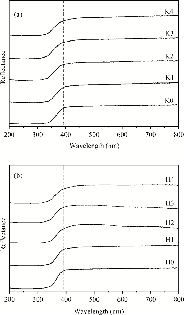
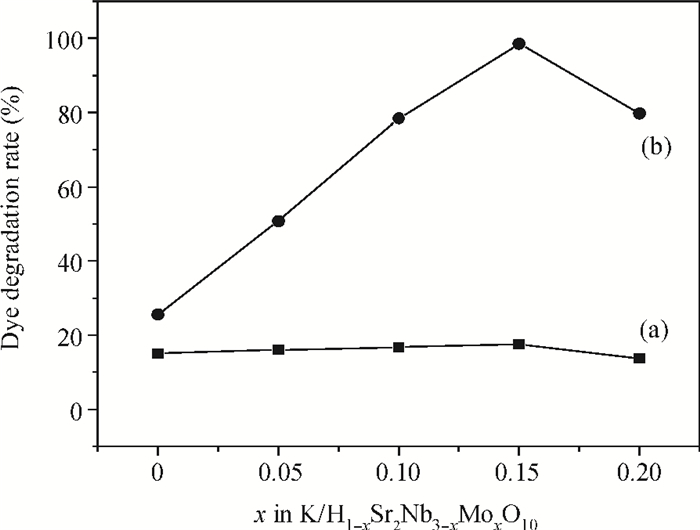
H1-xSr2Nb3-xMoxO10 photocatalysts were synthesized using a microwave-irradiation-assisted ion-exchange reaction. The physicochemical properties of the photocatalysts were analyzed by field-emission scanning electron microscopy (FE-SEM), X-ray diffraction (XRD) and ultraviolet-visible spectroscopy (UV-Vis). The photocatalytic activity of the H1-xSr2Nb3-xMoxO10 was evaluated by degrading methyl orange (MO) dye under light irradiation from a 40-W mercury lamp. The results proved that the Mo doping amount had an important effect on the photocatalytic activity of the catalysts. The highest photocatalytic activity was obtained when the doping amount was 15 mol%. Furthermore, the complex preparation process and lengthy time was simplified and shortened greatly.


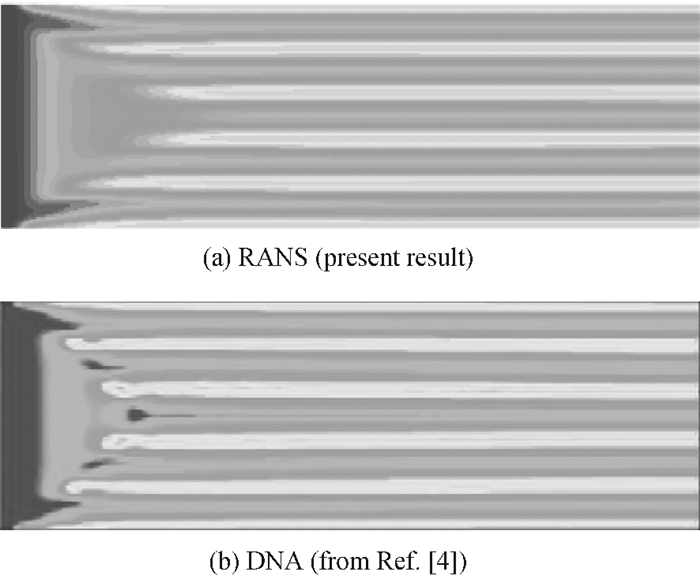
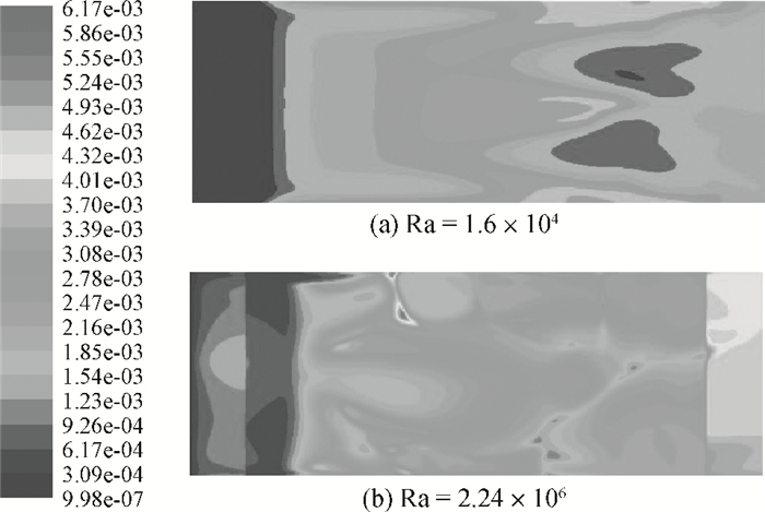
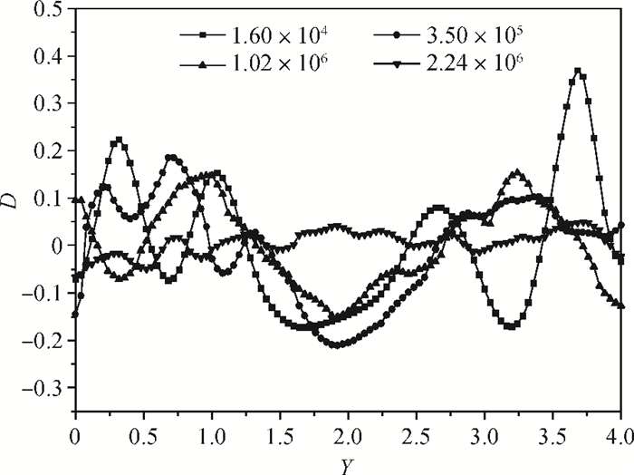
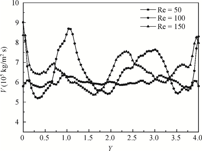
Numerical simulation, based on simple reaction models that manifest the deposition quality of silicon from silane, was undertaken to investigate the horizontal reactor, with longitudinal and transversal aspect ratios of 10 and 4, respectively. The effects of Rayleigh (Ra) and Reynolds (Re) numbers on the Si deposition rate in these turbulent-type reactors are discussed. The results show that the time-averaged deposition rate is fairly uniform and fast, although the instantaneous deposition is non-uniform in these turbulent reactors. In addition, the increase of the Re number within a certain range can compensate for the path loss of the reactant and obviously enhance the downstream deposition rate, but deteriorate the transverse distribution of the deposition.


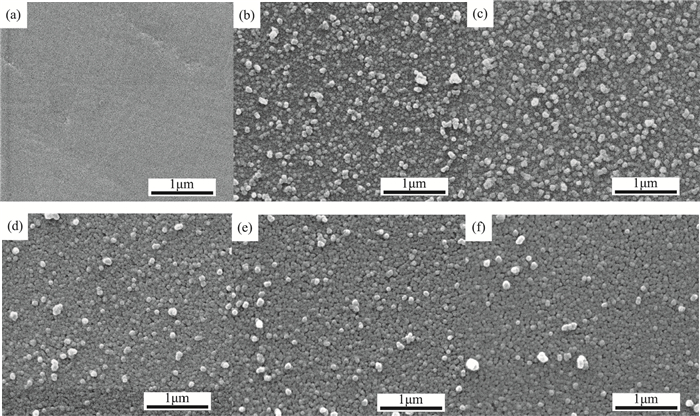
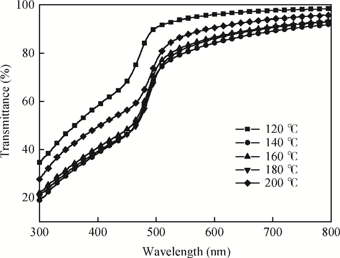
CdS thin films were successfully deposited onto glass substrates for the first time by the polyol method using cadmium acetate, thiourea and diethylene glycol as the raw materials. The effects of the deposition temperature from 120 to 200℃ in steps of 20℃ on the structure, morphology and optical properties of the resultant films were investigated. It was found that the crystallinity was improved and the value of the surface average roughness was decreased with increasing the deposition temperature. The average grain sizes of the CdS thin films were 77.16 and 76.61 nm at 140 and 180℃, respectively. All samples showed excellent transmittance and the band gaps were found to reduce from 2.55 to 2.45 eV with the increase of the deposition temperature, which was attributed to the improvement of crystallinity.


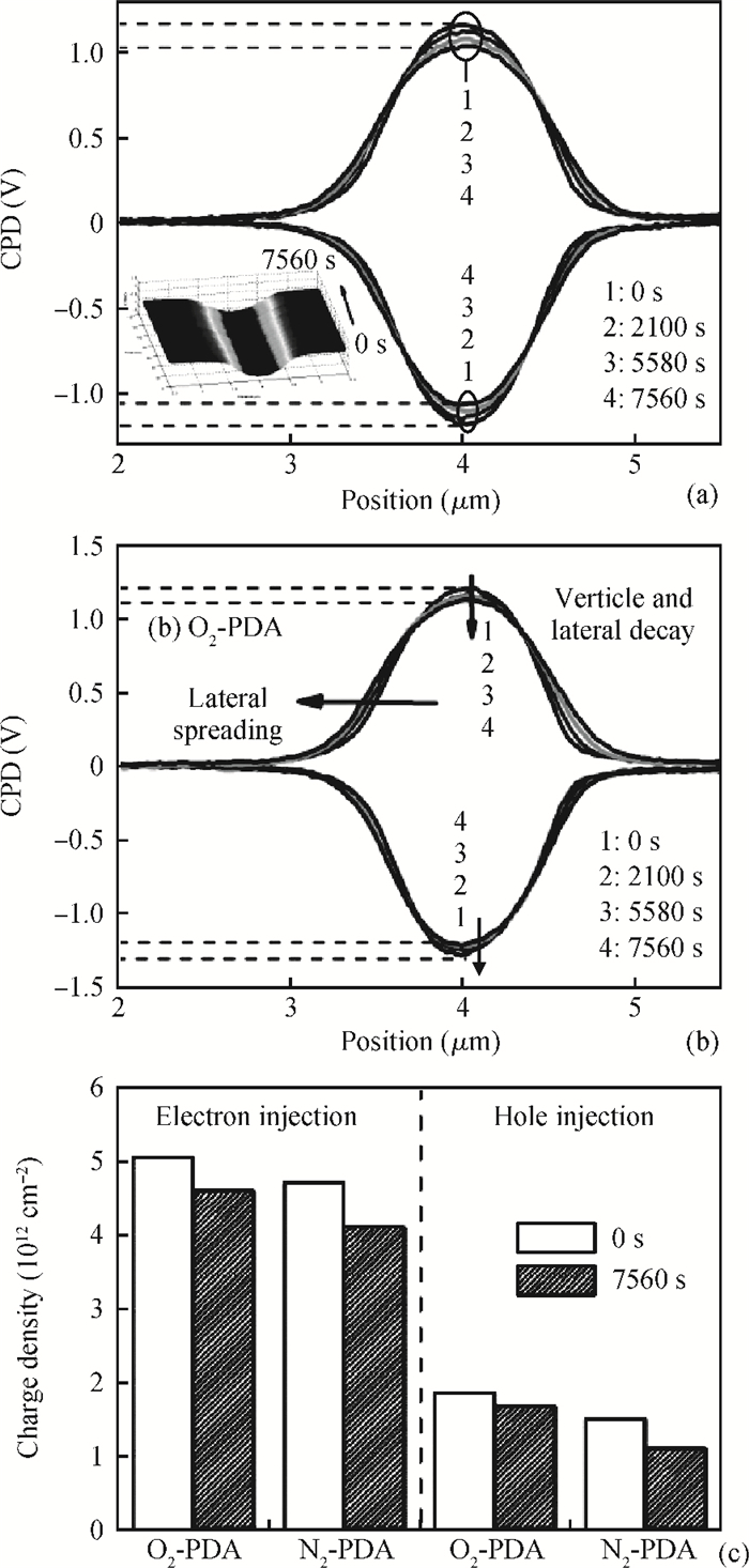
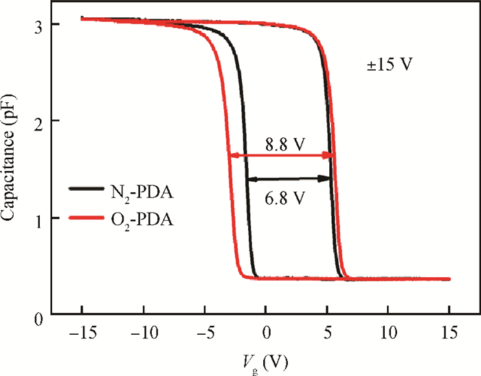
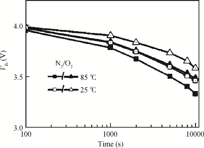
The retention characteristics of electrons and holes in hafnium oxide with post-deposition annealing in a N2 or O2 ambient were investigated by Kelvin probe force microscopy. The KFM results show that compared with the N2 PDA process, the O2 PDA process can lead to a significant retention improvement. Vertical charge leakage and lateral charge spreading both played an important role in the charge loss mechanisms. The retention improvement is attributed to the deeper trap energy. For electrons, the trap energy of the HOS structure annealed in a N2 or O2 ambient were determined to be about 0.44 and 0.49 eV, respectively. For holes, these are about 0.34 and 0.36 eV, respectively. Finally, the electrical characteristics of the memory devices are demonstrated from the experiment, which agreed with our characterization results. The qualitative and quantitative determination of the charge retention properties, the possible charge decay mechanism and trap energy reported in this work can be very useful for the characterization of hafnium charge storage devices.


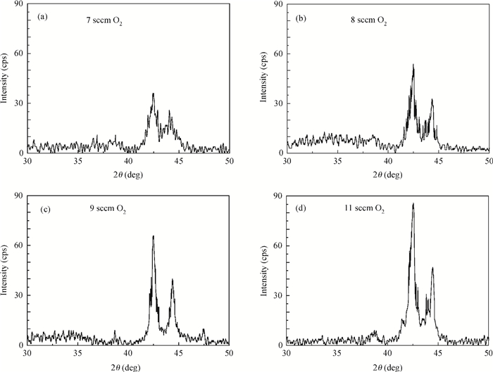
With RF sputtering process, Si/SiO2/Ta/Ru/Ta/CoFeB/MgO/CoFeB/Ta/Ru structure has been grown on Si (100) substrate. Attempting different targets and adjusting the oxygen dose, the crystallization quality of the MgO layer is studied. The X-ray diffraction measurements demonstrate that crystal structure and crystallization quality of MgO layers are related to the type of target and concentration of oxygen in sputtering process. With the method sputtering Mg in an ambient flow of oxygen, not only the crystallization quality of a normal MgO layer with lattice constant of 0.421 nm is improved, but also a new MgO crystal with lattice constant of 0.812 nm is formed and the perpendicular magnetic anisotropy of CoFeB is enhanced. Also it is found that crystallization quality for both the normal MgO and new MgO is more improved with MgO target and same oxygen dose, which means that this new method is helpful to form a new structure of MgO with lattice constant of 0.812 nm. All of the samples were annealed at 400℃ in vacuum.


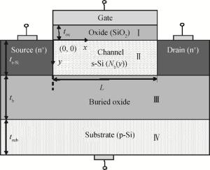
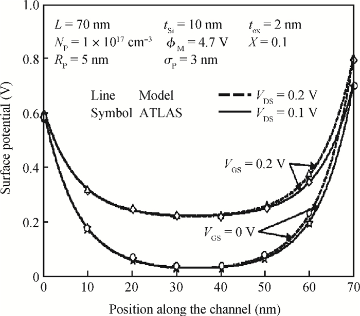
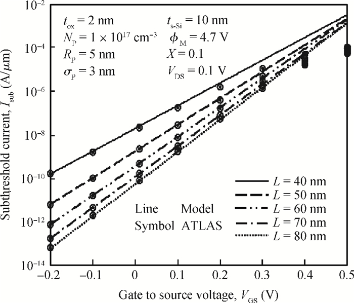
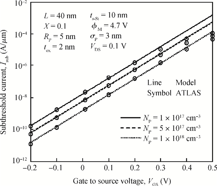
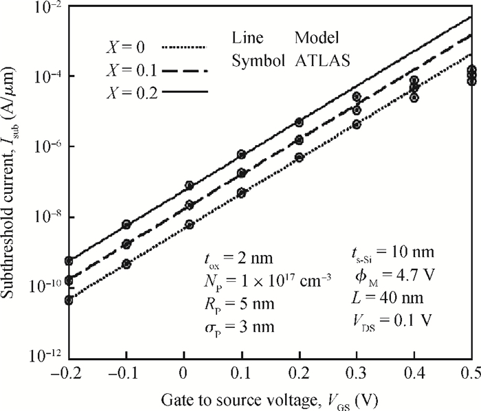
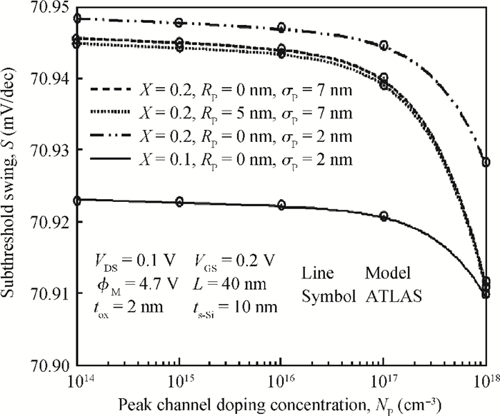
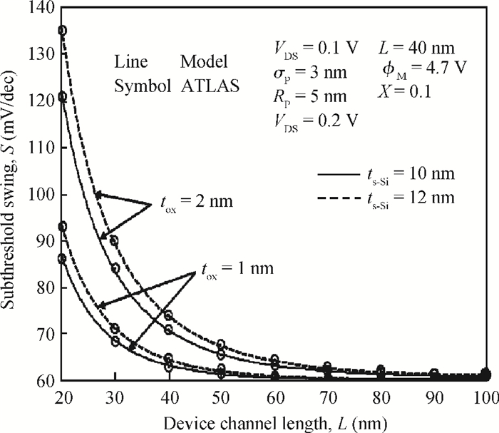
This paper presents the analytical modeling of subthreshold current and subthreshold swing of short-channel fully-depleted (FD) strained-Si-on-insulator (SSOI) MOSFETs having vertical Gaussian-like doping profile in the channel. The subthreshold current and subthreshold swing have been derived using the parabolic approximation method. In addition to the effect of strain on silicon layer, various other device parameters such as channel length (L), gate-oxide thickness (tox), strained-Si channel thickness (ts-Si), peak doping concentration (NP), project range (Rp) and straggle (σp) of the Gaussian profile have been considered while predicting the device characteristics. The present work may help to overcome the degradation in subthreshold characteristics with strain engineering. These subthreshold current and swing models provide valuable information for strained-Si MOSFET design. Accuracy of the proposed models is verified using the commercially available ATLASTM, a two-dimensional (2D) device simulator from SILVACO.


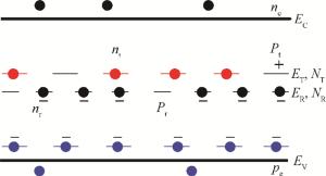
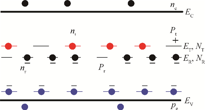
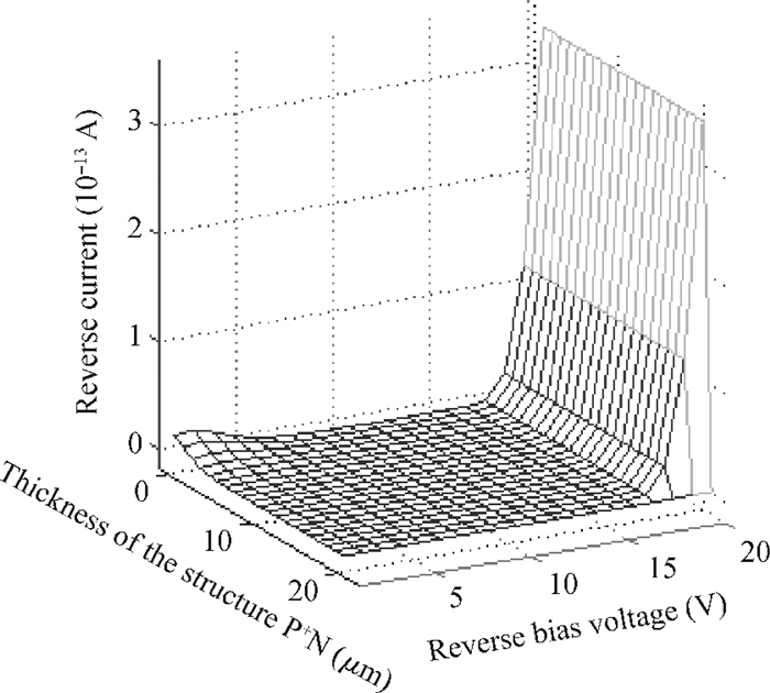
This work aims to determine the characteristic I (breakdown voltage) of the inverse current in a GaAs PN junction diode, subject to a reverse polarization, while specifying the parameters that influence the breakdown voltage of the diode. In this work, we simulated the behavior of the ionization phenomenon by impact breakdown by avalanche of the PN junctions, subject to an inverse polarization.We will take into account both the trapping model in a stationary regime in the P+N structure using like material of basis the Ⅲ-Ⅴ compounds and mainly the GaAs semi-insulating in which the deep centers have in important densities. We are talking about the model of trapping in the space charge region (SCR) and that is the trap density donor and acceptor states.The carrier crossing the space charge region (SCR) of W thickness creates N electron-hole pairs:for every created pair, the electron and the hole are swept quickly by the electric field, each in an opposite direction, which comes back, according to an already accepted reasoning, to the crossing of the space charge region (SCR) by an electron or a hole. So the even N pair created by the initial particle provoke N2 ionizations and so forth.The study of the physical and electrical behaviour of semiconductors is based on the influence of the presence of deep centers on the characteristic I(V) current-tension, which requires the calculation of the electrostatic potential, the electric field, the integral of ionization, the density of the states traps, the diffusion current of minority in the regions (1) and (3), the current thermal generation in the region (2), the leakage current in the surface, and the breakdown voltage.


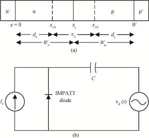
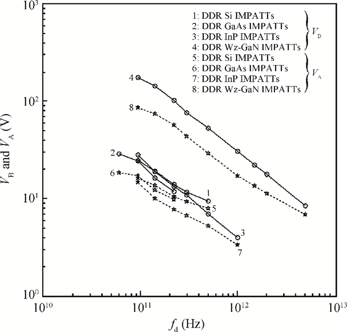
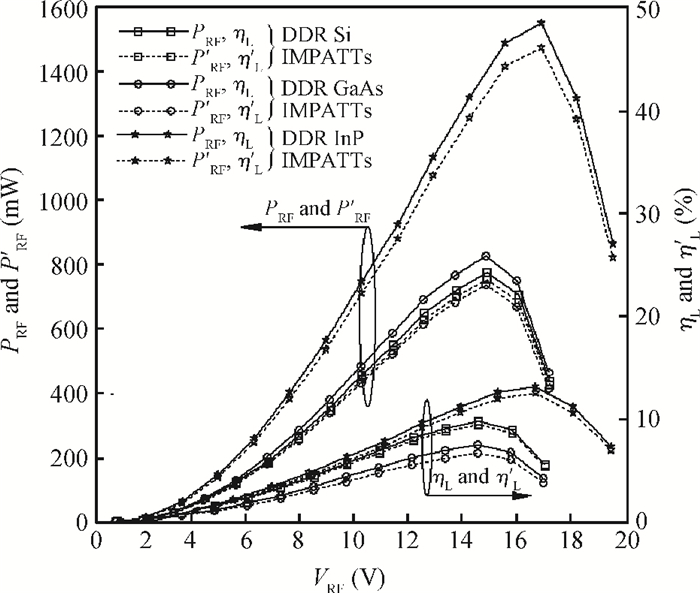
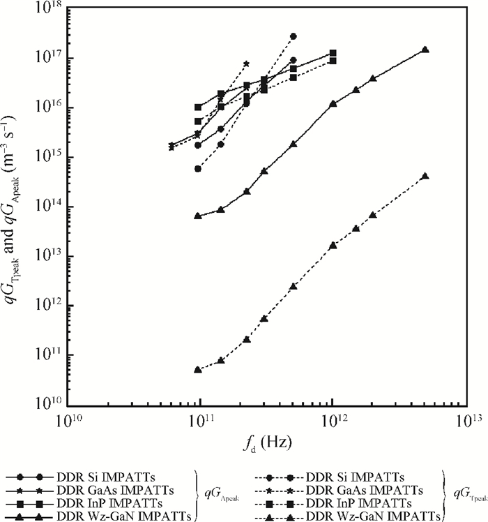
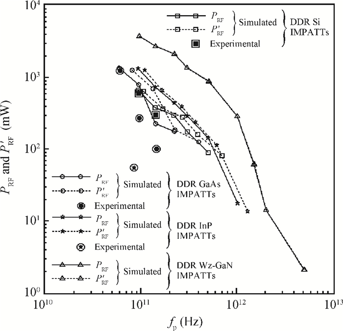
Large-signal (L-S) characterizations of double-drift region (DDR) impact avalanche transit time (IMPATT) devices based on group Ⅲ-Ⅴ semiconductors such as wurtzite (Wz) GaN, GaAs and InP have been carried out at both millimeter-wave (mm-wave) and terahertz (THz) frequency bands. A L-S simulation technique based on a non-sinusoidal voltage excitation (NSVE) model developed by the authors has been used to obtain the high frequency properties of the above mentioned devices. The effect of band-to-band tunneling on the L-S properties of the device at different mm-wave and THz frequencies are also investigated. Similar studies are also carried out for DDR IMPATTs based on the most popular semiconductor material, i.e. Si, for the sake of comparison. A comparative study of the devices based on conventional semiconductor materials (i.e. GaAs, InP and Si) with those based on Wz-GaN shows significantly better performance capabilities of the latter at both mm-wave and THz frequencies.


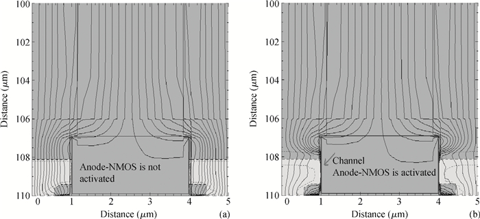
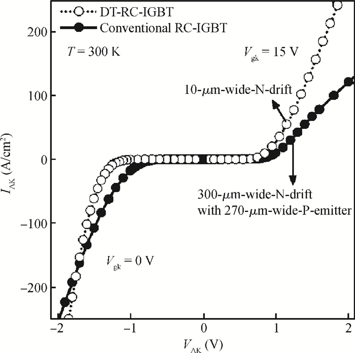
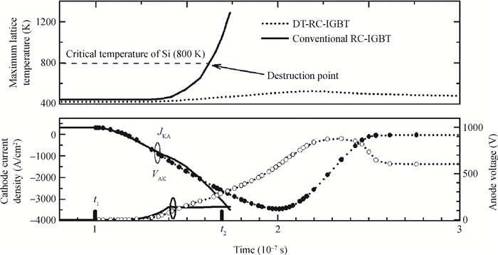
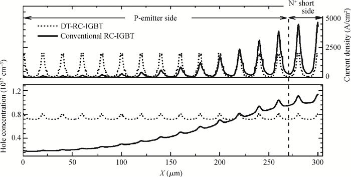
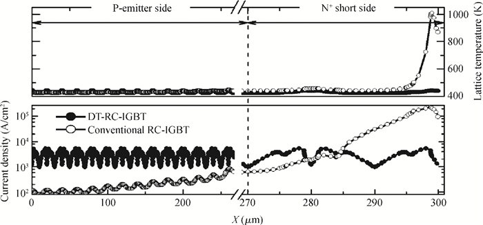
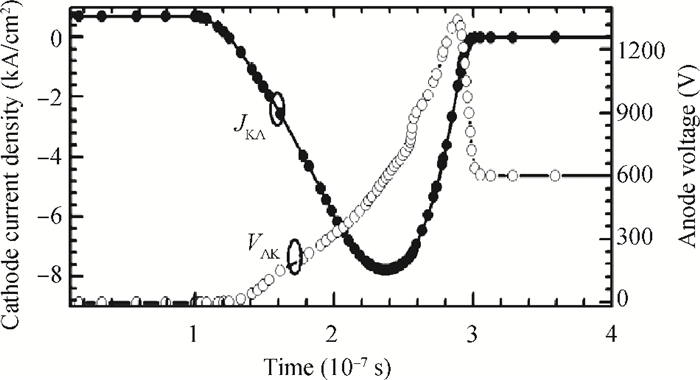
The phenomenon that the wide P-emitter region in the conventional reverse conducting insulated gate bipolar transistor (RC-IGBT) results in the non-uniform current distribution in the integrated freewheeling diode (FWD), and then causes a parasitic thyristor to latch-up during its reverse-recovery process, which induces a hot spot in the local region of the device is revealed for the first time. Furthermore, a novel RC-IGBT based on double trench IGBT is proposed. It not only solves the snapback problem but also has uniform current distribution and high ruggedness during the reverse-recovery process.


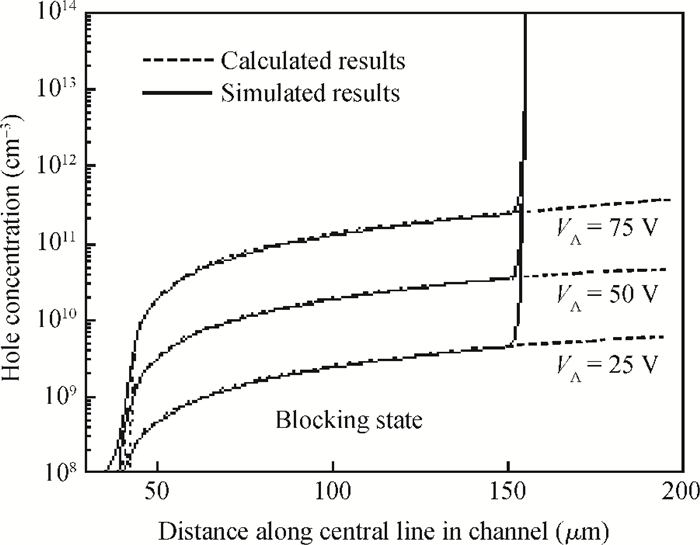
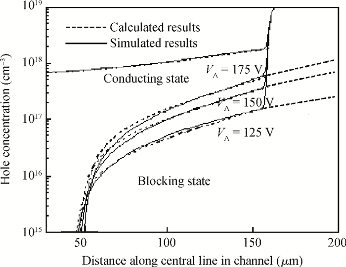
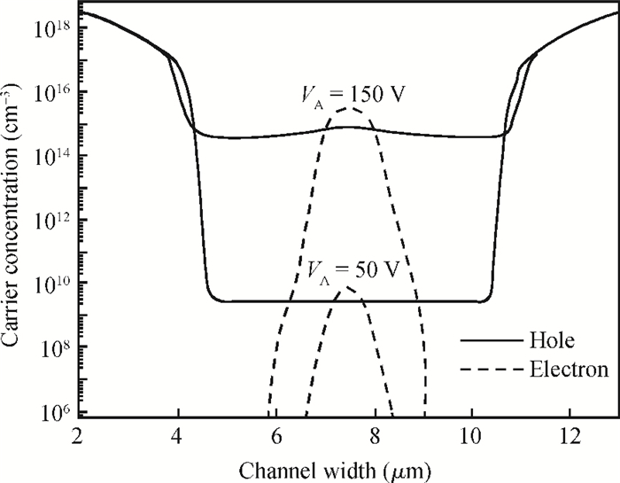
The physical effects of the carrier distribution in the channel on the dynamical performance of a static induction thyristor (SITH) have been studied numerically and experimentally. The analytical expressions of the minority carrier distribution in the channel of the SITH were also derived and the space charge distribution controlling mechanism on the current of the SITH under high level injection have been analyzed deeply. The relationships among the minority carrier distribution, potential distribution, I-V characteristics and transient performances of the SITH are revealed.

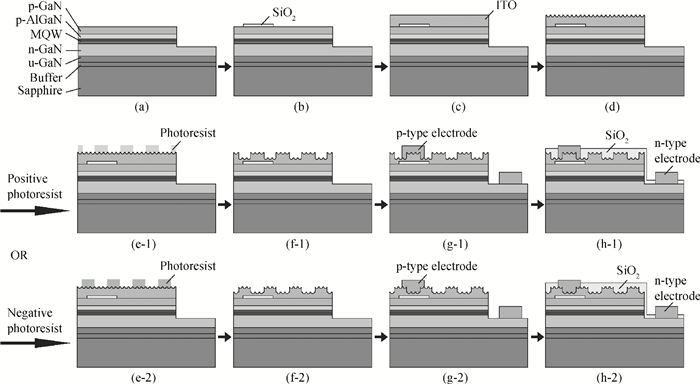
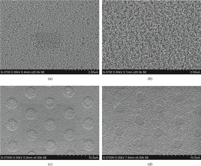
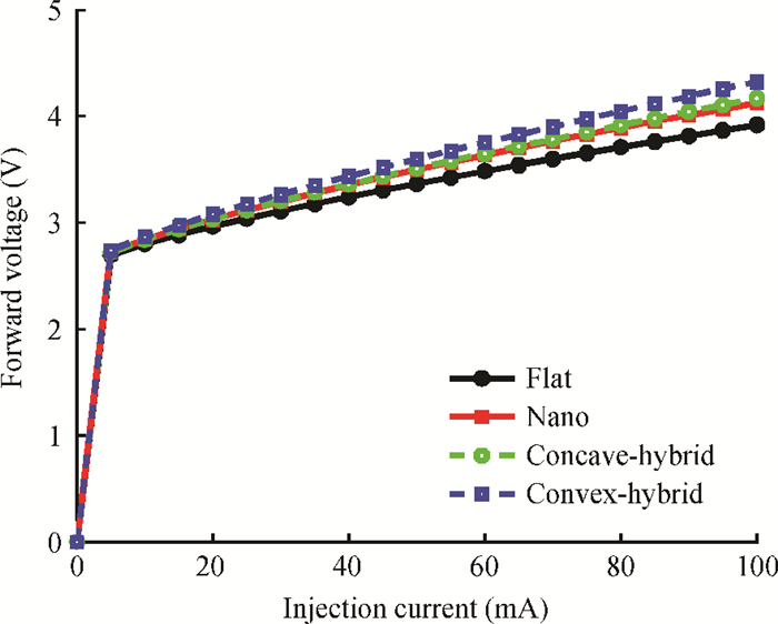
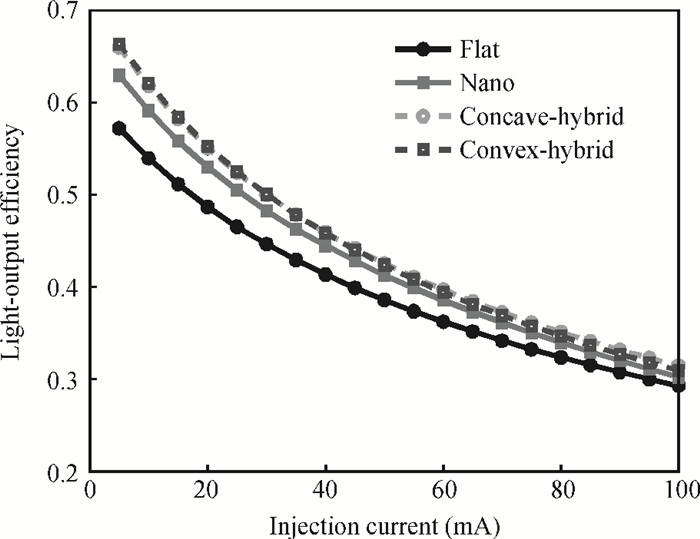
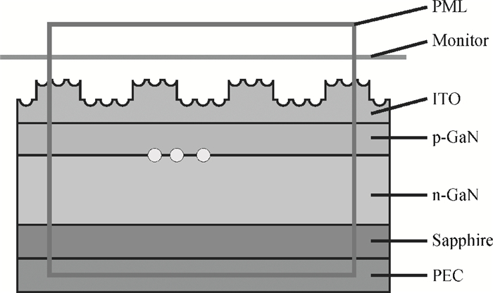
Three types of textured indium-tin-oxide (ITO) surface, including nano-texturing and hybrid micro/nano-texturing with micro-holes (concave-hybrid-pattern) or micro-pillars (convex-hybrid-pattern), were applied to GaN-based light-emitting diodes (LEDs). The nano-texturing was realized by maskless wet-etching, and the micro-texturing was achieved by standard photolithography and wet-etching. Compared to LED chips with flat ITO surface, those with nano-pattern, concave-hybrid-pattern, and convex-hybrid-pattern exhibit enhancement of 11.3%, 15.8%, and 17.9%, respectively, for the light-output powers at 20 mA. The electrical performance has no degradation. Moreover, the convex-hybrid-pattern show higher light-output efficiency under small injection current, while the concave-hybrid-pattern exhibit better light-output efficiency at large injection current. The light-extraction efficiency is simulated by use of two-dimensional finite difference time domain method, and the numerical results are consistent with the experiments.

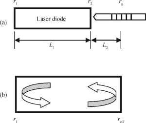
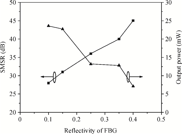
The coupling cavity theory is used to analyze the impact of high side mode suppression ratio (SMSR) on fiber grating external cavity semiconductor lasers (FGECSL). The high SMSR and high stable frequency FGECSLs were obtained by experiment. The center wavelength is 974 nm, SMSR is 45 dB, the center wavelength change rate reaches 3.08 ppm/℃ in the temperature range of -20 to 80℃.


The temperature dependence of single event upset (SEU) measurement both in commercial bulk and silicon on insulator (SOI) static random access memories (SRAMs) has been investigated by experiment in the Heavy Ion Research Facility in Lanzhou (HIRFL). For commercial bulk SRAM, the SEU cross section measured by 12C ions is very sensitive to the temperature. The temperature test of SEU in SOI SRAM was conducted by 209Bi and 12C ions, respectively, and the SEU cross sections display a remarkable growth with the elevated temperature for 12C ions but keep constant for 209Bi ions. The impact of temperature on SEU measurement was analyzed by Monte Carlo simulation. It is revealed that the SEU cross section is significantly affected by the temperature around the threshold linear energy transfer of SEU occurrence. As the SEU occurrence approaches saturation, the SEU cross section gradually exhibits less temperature dependency. Based on this result, the experimental data measured in HIRFL was analyzed, and then a reasonable method of predicting the on-orbit SEU rate was proposed.


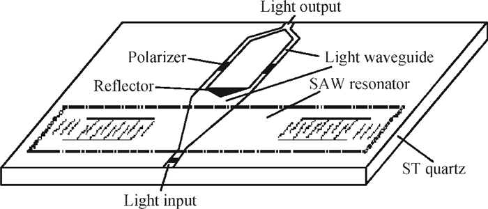
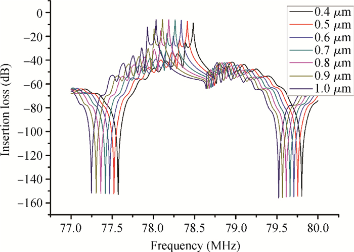
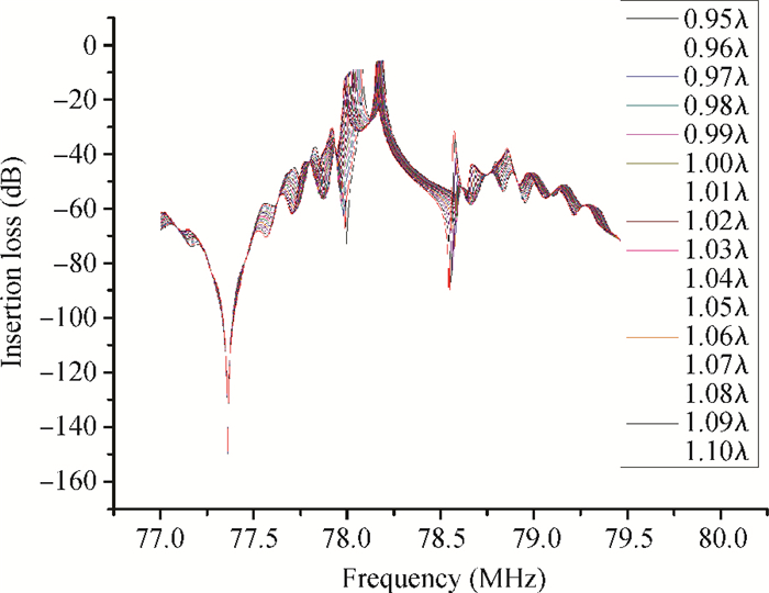
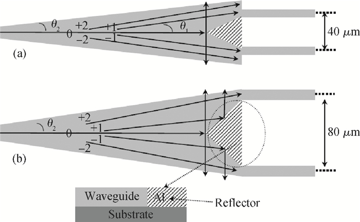
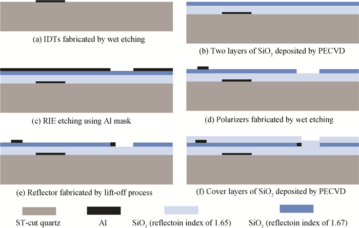
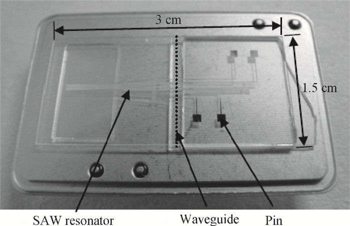
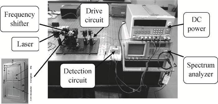
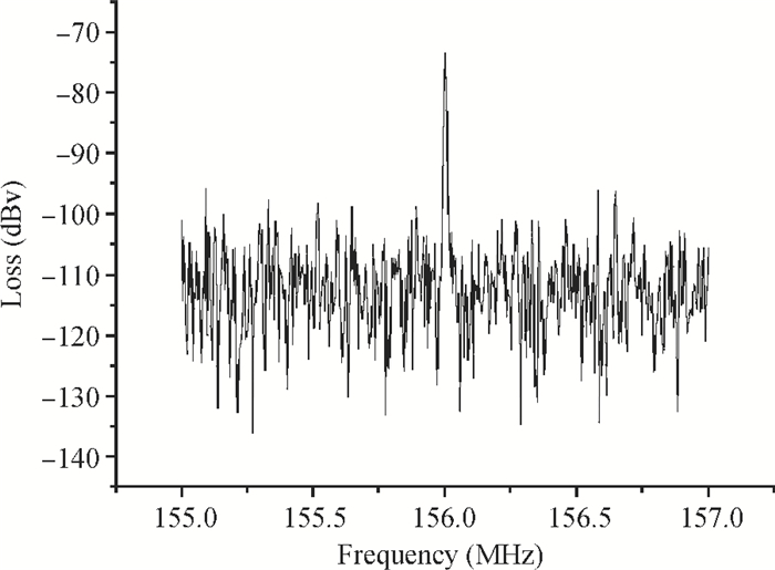
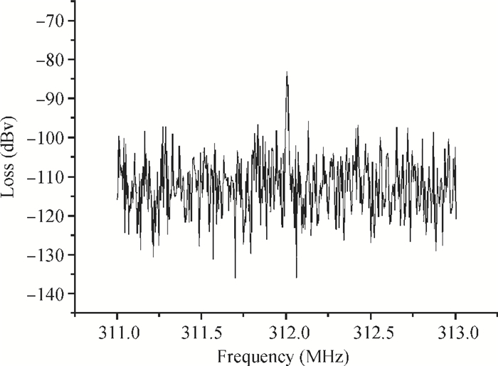
A Raman acousto-optic frequency shifter (AOFS) based on surface acoustic wave (SAW) is presented. It consists of a double-ended SAW resonator and optical waveguide system. The structure parameters of the SAW resonator are optimized using COM software and the optical waveguide system is designed using an effective index method. The AOFS prototype fabricated using MEMS technology is detected. The optical beat signals superimposed by ±1st-order and ±2nd-order diffracted beams are detected. The frequency shift of 78.2201 MHz related to the 1st-order diffracted beams and 156.2306 MHz related to the 2nd-order diffracted beams are obtained respectively.


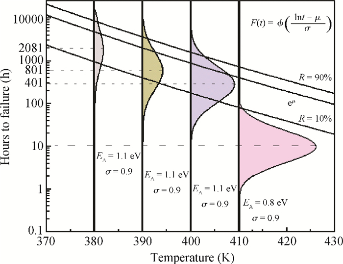
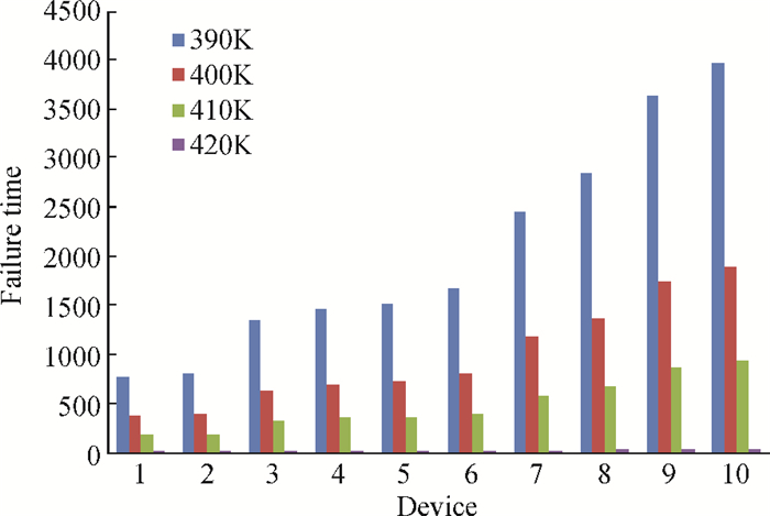
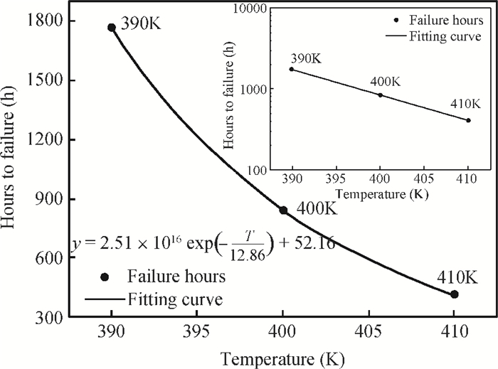
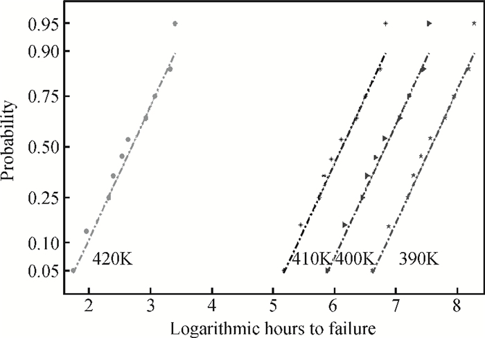
The failure mechanism stimulated by accelerated stress in the degradation may be different from that under normal conditions, which would lead to invalid accelerated life tests. To solve the problem, we study the relation between the Arrhenius equation and the lognormal distribution in the degradation process. Two relationships of the lognormal distribution parameters must be satisfied in the conclusion of the unaltered failure mechanism, the first is that the logarithmic standard deviations must be equivalent at different temperature levels, and the second is that the ratio of the differences between logarithmic means must be equal to the ratio of the differences between reciprocals of temperature. The logarithm of distribution lines must simultaneously have the same slope and regular interval lines. We studied the degradation of thick-film resistors in MCM by accelerated stress at four temperature levels (390, 400, 410 and 420 K), and the result agreed well with our method.


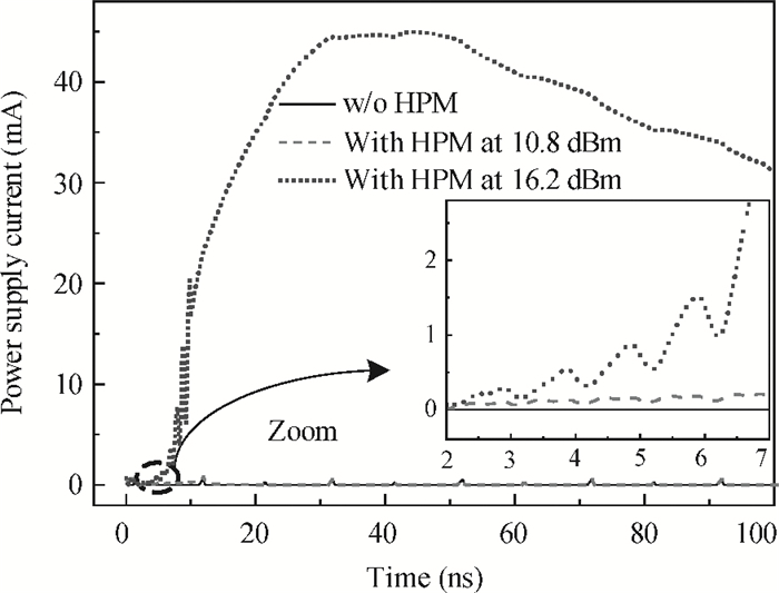
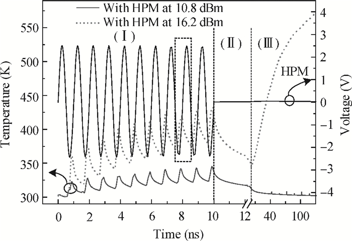
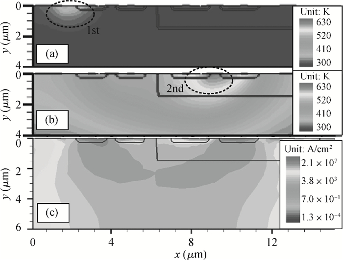
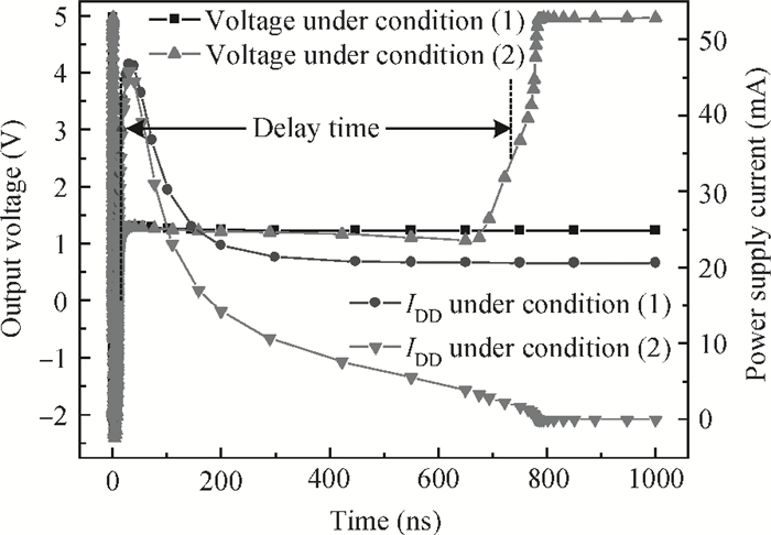
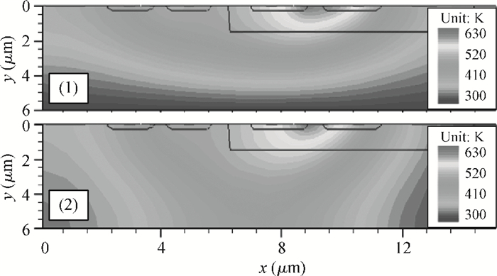
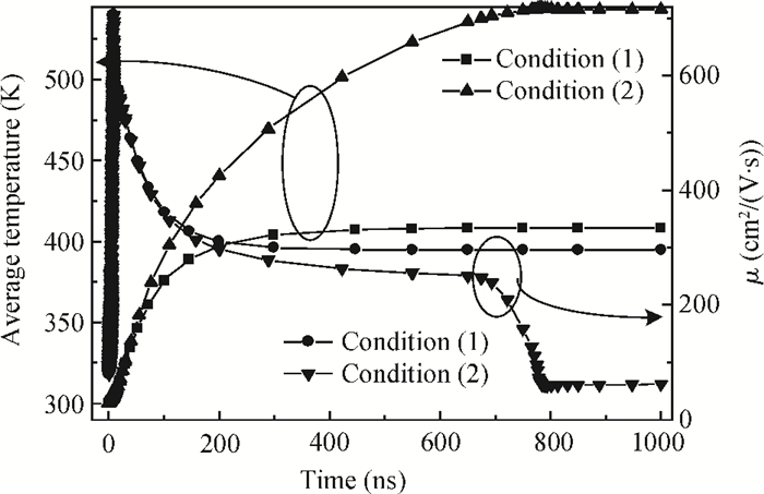
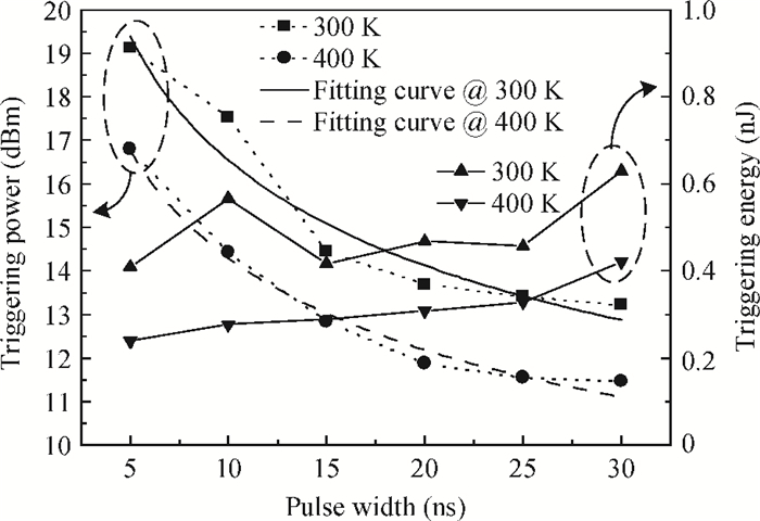
The temperature dependence of the latch-up effects in a CMOS inverter based on 0.5 μm technology caused by high power microwave (HPM) is studied. The malfunction and power supply current characteristics are revealed and adopted as the latch-up criteria. The thermal effect is shown and analyzed in detail. CMOS inverters operating at high ambient temperature are confirmed to be more susceptible to HPM, which is verified by experimental results from previous literature. Besides the dependence of the latch-up triggering power P on the ambient temperature T follows the power-law equation P=ATβ. Meanwhile, the ever reported latch-up delay time characteristic is interpreted to be affected by the temperature distribution. In addition, it is found that the power threshold increases with the decrease in pulse width but the degree of change with a certain pulse width is constant at different ambient temperatures. Also, the energy absorbed to cause latch-up at a certain temperature is basically sustained at a constant value.


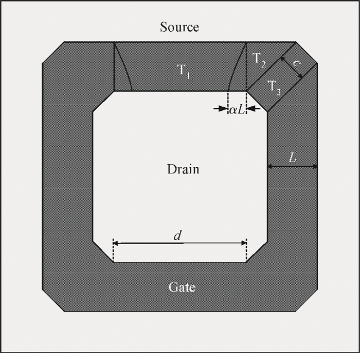
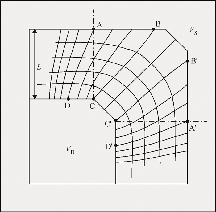
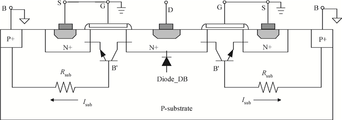
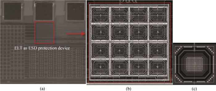
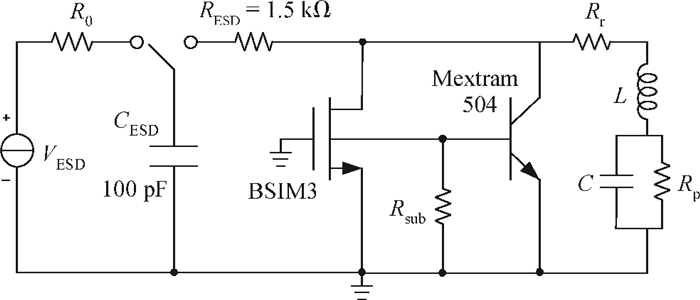
This paper proposes a novel technique for modeling the electrostatic discharge (ESD) characteristic of the enclosed-gate layout transistors (ELTs). The model consists of an ELT, a parasitic bipolar transistor, and a substrate resistor. The ELT is decomposed into edge and corner transistors by solving the electrostatic field problem through the conformal mapping method, and these transistors are separately modeled by BSIM (Berkeley Short-channel IGFET Model). Fast simulation speed and easy implementation is obtained as the model can be incorporated into standard SPICE simulation. The model parameters are extracted from the critical point of the snapback curve, and simulation results are presented and compared to experimental data for verification.


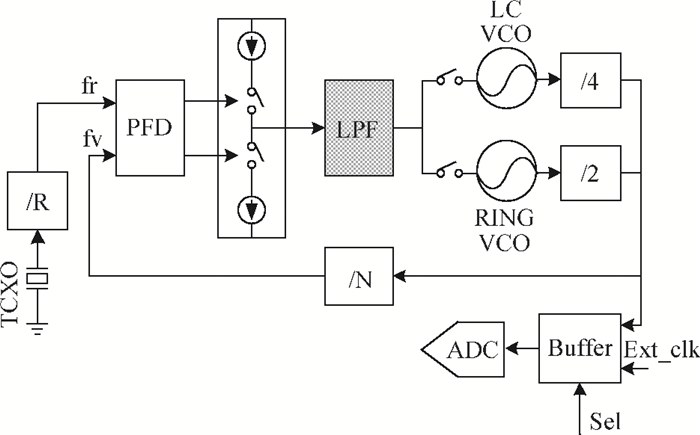
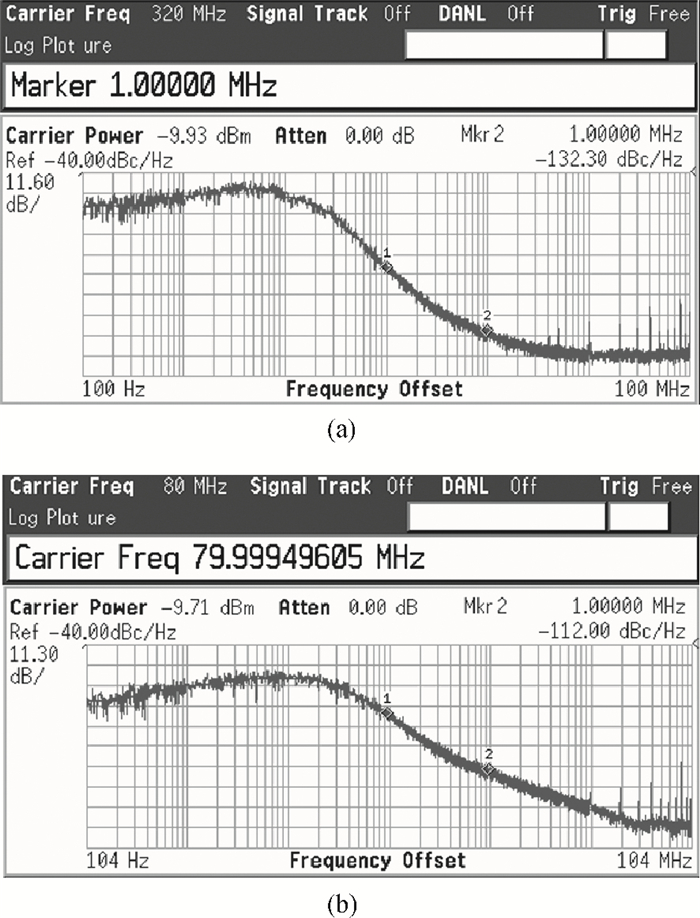
A 35-130 MHz/300-360 MHz phase-locked loop frequency synthesizer for Δ-Σ analog-to-digital converter (ADC) in 65 nm CMOS is presented. The frequency synthesizer can work in low phase-noise mode (300-360 MHz) or in low-power mode (35-130 MHz) to satisfy the ADC's requirements. To switch between these two modes, a high frequency GHz LC VCO followed by a divided-by-four frequency divider and a low frequency ring VCO followed by a divided-by-two frequency divider are integrated on-chip. The measured results show that the frequency synthesizer achieves a phase-noise of -132 dBc/Hz at 1 MHz offset and an integrated RMS jitter of 1.12 ps with 1.74 mW power consumption from a 1.2 V power supply in low phase-noise mode. In low-power mode, the frequency synthesizer achieves a phase-noise of -112 dBc/Hz at 1 MHz offset and an integrated RMS jitter of 7.23 ps with 0.92 mW power consumption from a 1.2 V power supply.


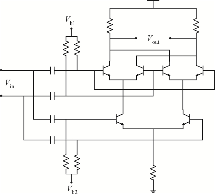
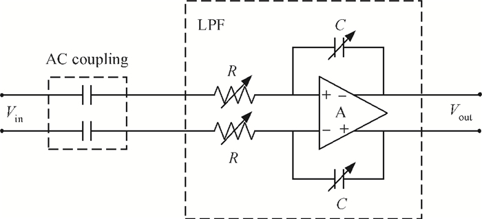
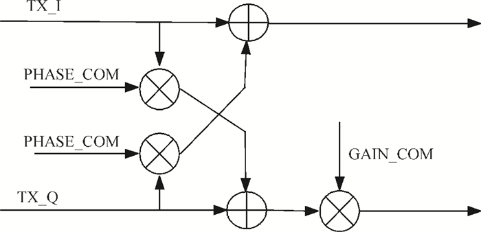
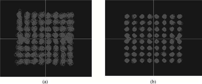
An IQ mismatch calibration and compensation technique based on the digital baseband for wideband wireless communication transmitters is proposed. The digital baseband transmits the signal used for IQ mismatch calibration. The signal passes through the RF transmitter path, the calibration loop (which is composed of a square power detector and a band-pass filter in the RF transceiver) and the variable gain amplifier of the receiver. The digital baseband samples the signal for IQ mismatch estimation and compensates for it. Compared with the self-calibration technique in the RF chip, the proposed technique saves area and power consumption for the wireless local area network solution. This technique has been successfully used for the 802.11n system and satisfies the requirement of the standard by achieving over 50 dB image suppression.


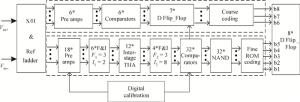
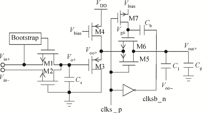
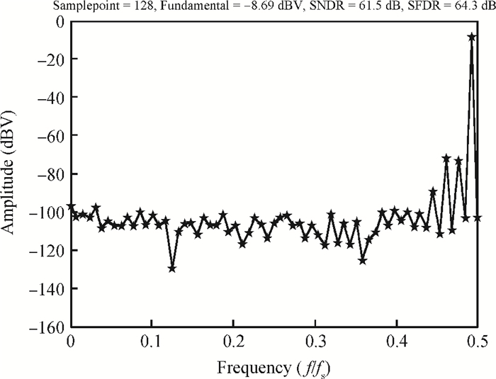
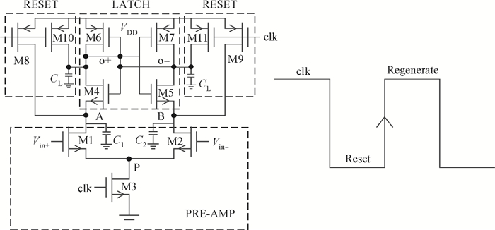
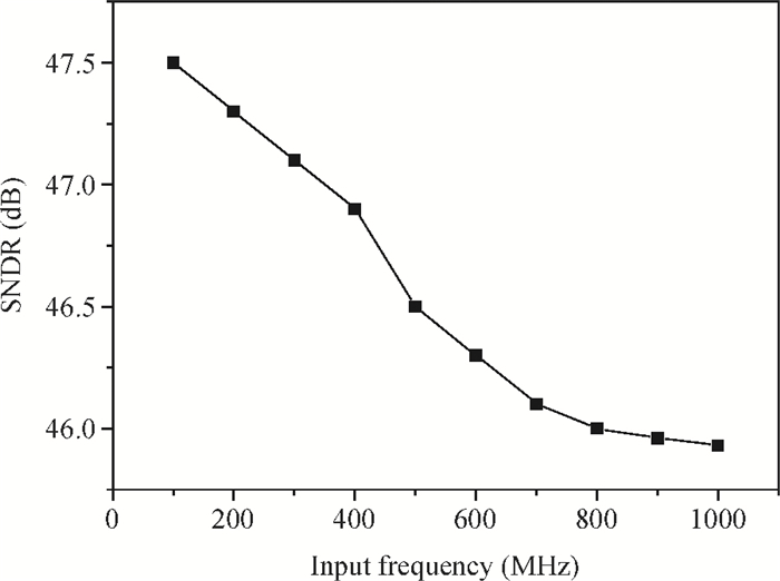
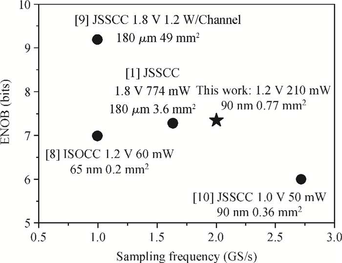
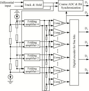
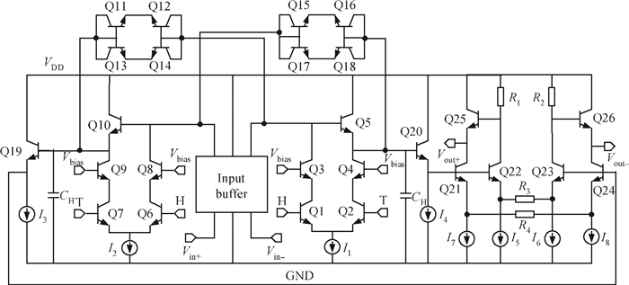
A single-channel 2 GS/s 8-bit analog-to-digital converter in 90 nm CMOS process technology is presented. It utilizes cascade folding architecture, which incorporates an additional inter-stage sample-and-hold amplifier between the folding circuits to enhance the quantization time. It also uses the foreground on-chip digital-assisted calibration circuit to improve the linearity of the circuit. The post simulation results demonstrate that it has a differential nonlinearity < ±0.3 LSB and an integral nonlinearity < ±0.25 LSB at the Nyquist frequency. Moreover, 7.338 effective numbers of bits can be achieved at 2 GSPS. The whole chip area is 0.88×0.88 mm2 with the pad. It consumes 210 mW from a 1.2 V single supply.


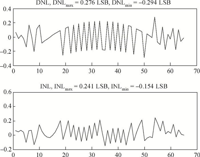
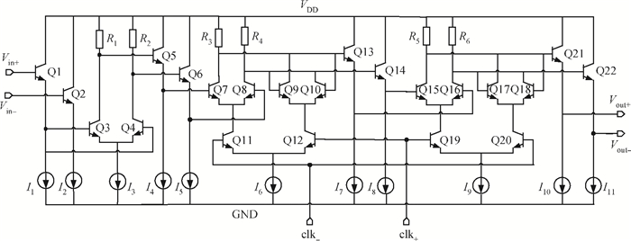
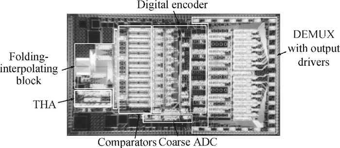
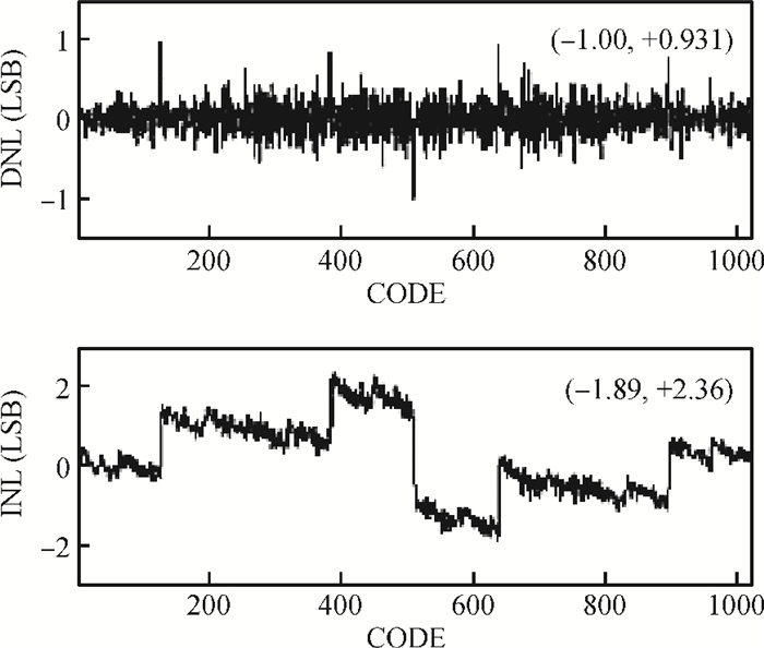
The design and test results of a 6-bit 3-Gsps analog-to-digital converter (ADC) using 1 μm GaAs heterojunction bipolar transistor (HBT) technology are presented. The monolithic folding-interpolating ADC makes use of a track-and-hold amplifier (THA) with a highly linear input buffer to maintain a highly effective number of bits (ENOB). The ADC occupies an area of 4.32×3.66 mm2 and achieves 5.53 ENOB with an effective resolution bandwidth of 1.1 GHz at a sampling rate of 3 Gsps. The maximum DNL and INL are 0.36 LSB and 0.48 LSB, respectively.


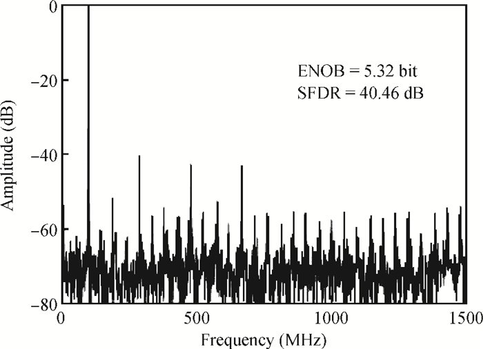
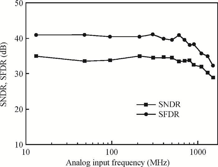

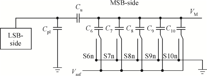
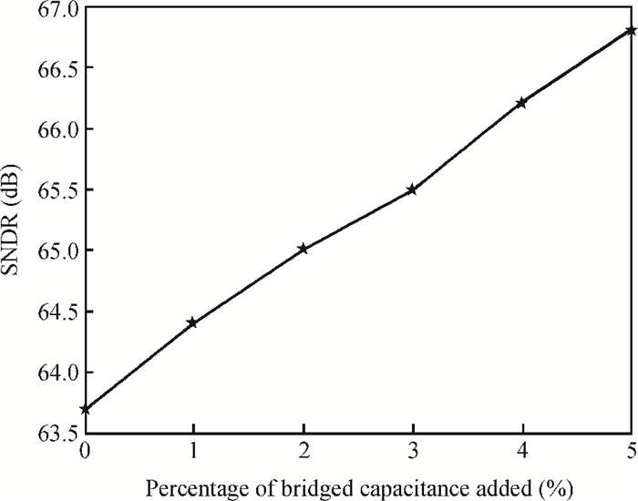
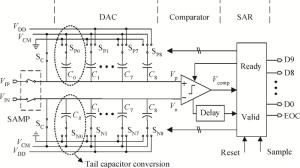
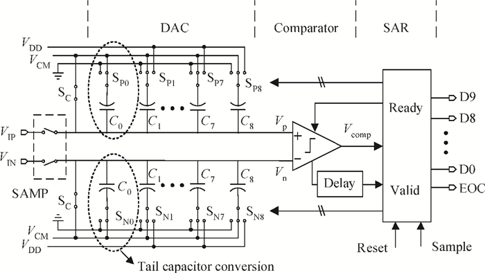
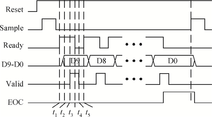
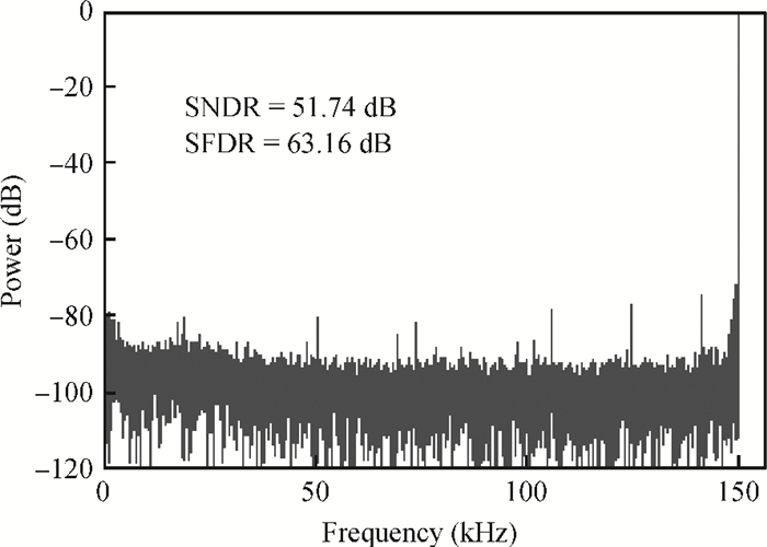
This paper presents an 11-bit 22-MS/s 0.6-mW successive approximation register (SAR) analog-to-digital converter (ADC) using SMIC 65-nm low leakage (LL) CMOS technology with a 1.2 V supply voltage. To reduce the total capacitance and core area the split capacitor architecture is adopted. But in high resolution ADCs the parasitic capacitance in the LSB-side would decrease the linearity of the ADC and it is hard to calibrate. This paper proposes a parasitic capacitance compensation technique to cancel the effect with no calibration circuits. Moreover, dynamic circuits are used to minimize the switching power of the digital logic and also can reduce the latency time. The prototype chip realized an 11-bit SAR ADC fabricated in SMIC 65-nm CMOS technology with a core area of 300×200 μm2. It shows a sampling rate of 22 MS/s and low power dissipation of 0.6 mW at a 1.2 V supply voltage. At low input frequency the signal-to-noise-and-distortion ratio (SNDR) is 59.3 dB and the spurious-free dynamic range is 72.2 dB. The peak figure-of-merit is 36.4 fJ/conversion-step.


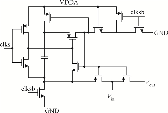

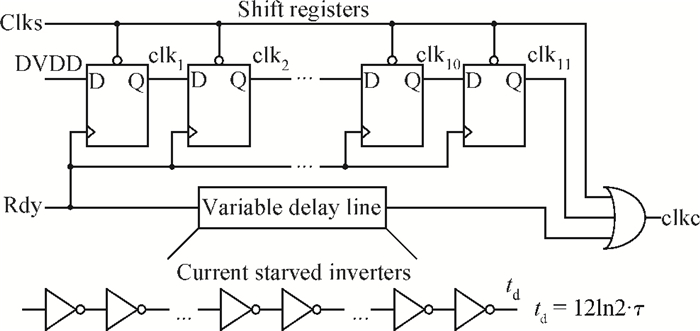


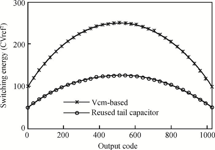
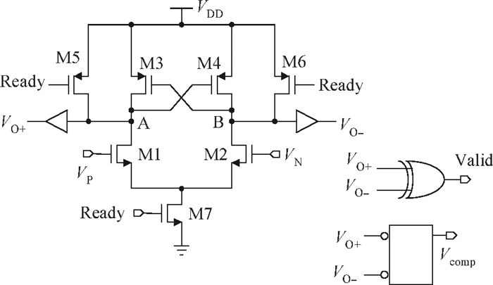
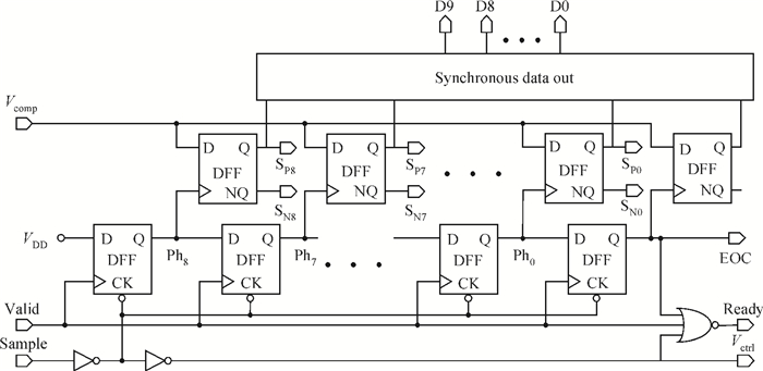
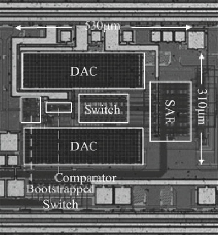
A microwatt asynchronous successive approximation register (SAR) analog-to-digital converter (ADC) is presented. The supply voltage of the SAR ADC is decreased to 0.6 V to fit the low voltage and low power requirements of biomedical systems. The tail capacitor of the DAC array is reused for least significant bit conversion to decrease the total DAC capacitance thus reducing the power. Asynchronous control logic avoids the high frequency clock generator and further reduces the power consumption. The prototype ADC is fabricated with a standard 0.18 μm CMOS technology. Experimental results show that it achieves an ENOB of 8.3 bit at a 300-kS/s sampling rate. Very low power consumption of 3.04 μW is achieved, resulting in a figure of merit of 32 fJ/conv.-step.


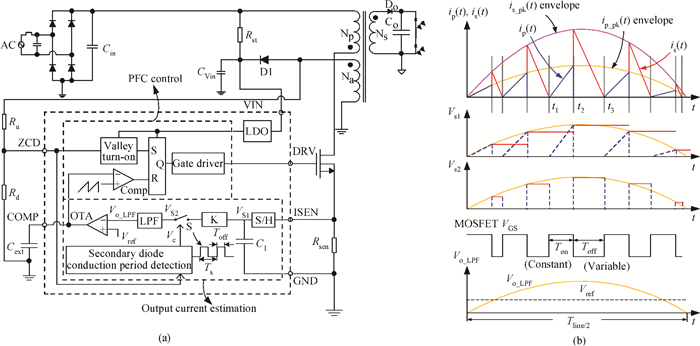
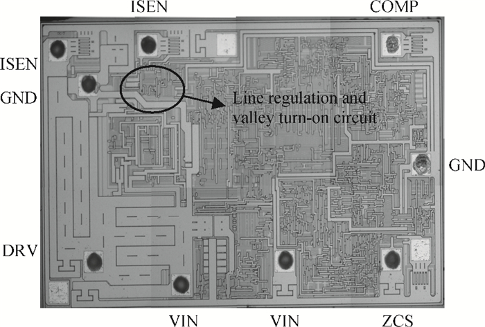
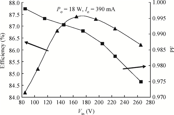
A single-stage flyback driving integrated circuit (IC) for light-emitting diodes (LEDs) is proposed. With an average primary-side current estimation and negative feedback networks, the driver operates in the boundary conduction mode (BCM), while the output current can be derived and regulated precisely. By means of a simple external resistor divider, a compensation voltage is produced on the ISEN pin during the turn-on period of the primary MOSFET to improve the line regulation performance. On the other hand, since the delay time between the time that the secondary diode current reaches zero and the turn-on time of the MOSFET can be automatically adjusted, the MOSFET can always turn on at the valley voltage even if the inductance of the primary winding varies with the output power, resulting in quasi-resonant switching for different primary inductances. The driving IC is fabricated in a Dongbu HiTek's 0.35 μm bipolar-CMOS-DMOS process. An 18 W LED driver is finally built and tested. Results show that the driver has an average efficiency larger than 86%, a power factor larger than 0.97, and works under the universal input voltage (85-265 V) with the LED current variation within ±0.5%.


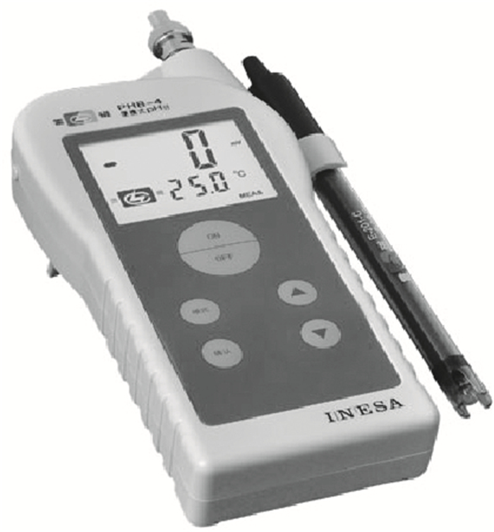
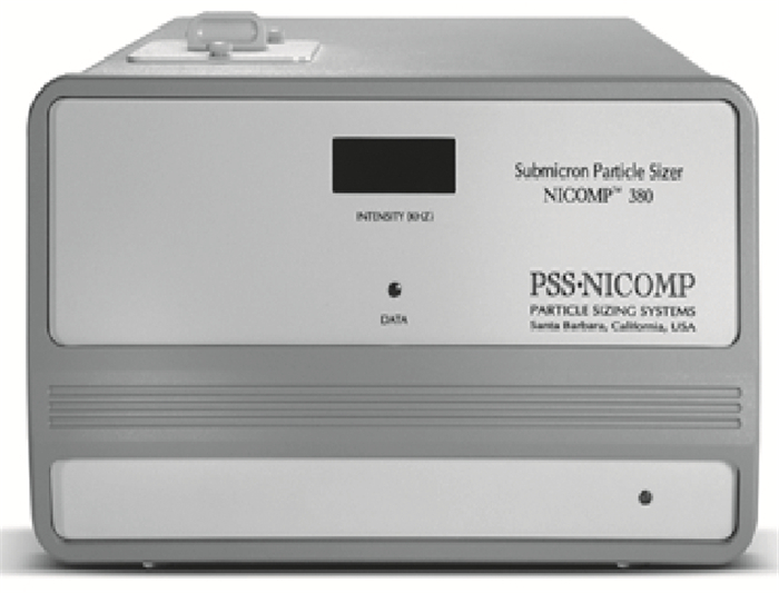
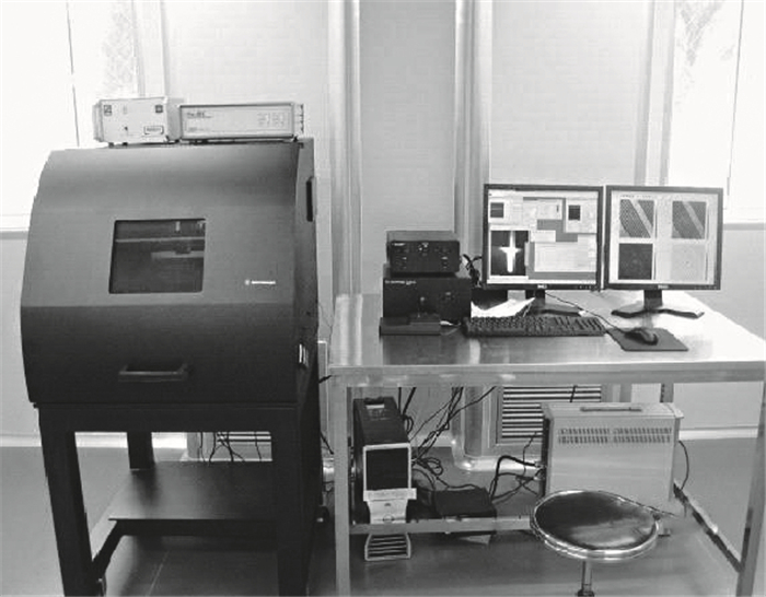
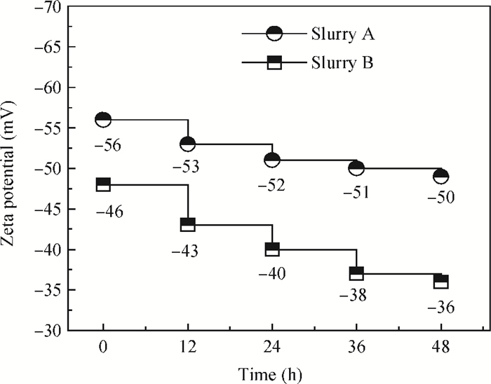
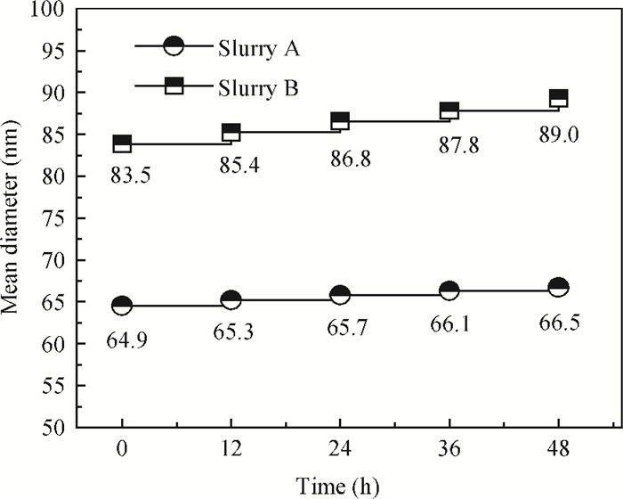
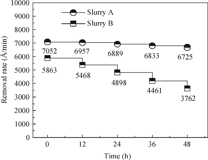
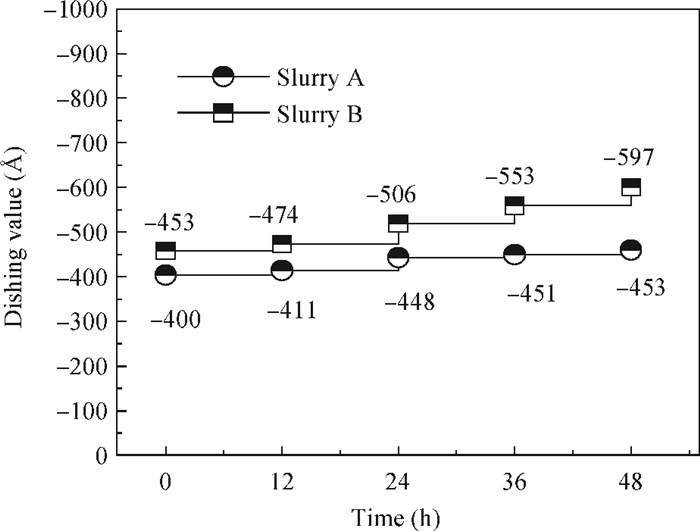
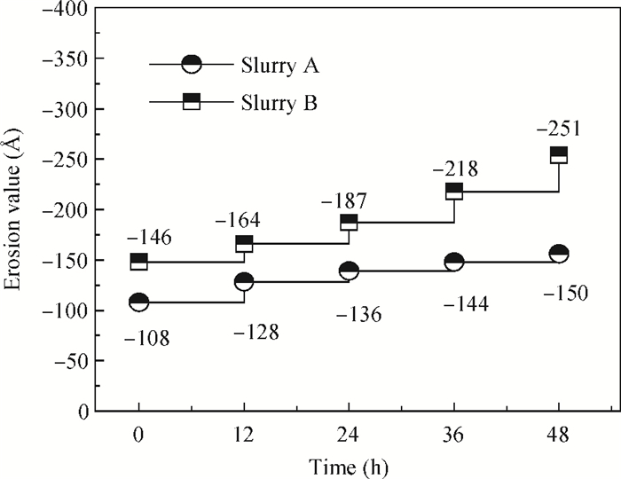
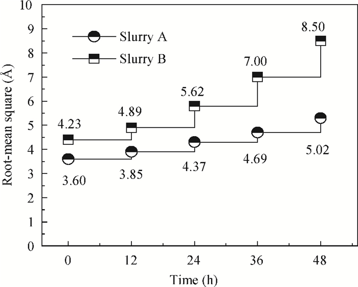
The stability of a novel low-pH alkaline slurry (marked as slurry A, pH=8.5) for copper chemical mechanical planarization was investigated in this paper. First of all, the stability mechanism of the alkaline slurry was studied. Then many parameters have been tested for researching the stability of the slurry through comparing with a traditional alkaline slurry (marked as slurry B, pH=9.5), such as the pH value, particle size and zeta potential. Apart from this, the stability of the copper removal rate, dishing, erosion and surface roughness were also studied. All the results show that the stability of the novel low-pH alkaline slurry is better than the traditional alkaline slurry. The working-life of the novel low-pH alkaline slurry reaches 48 h.