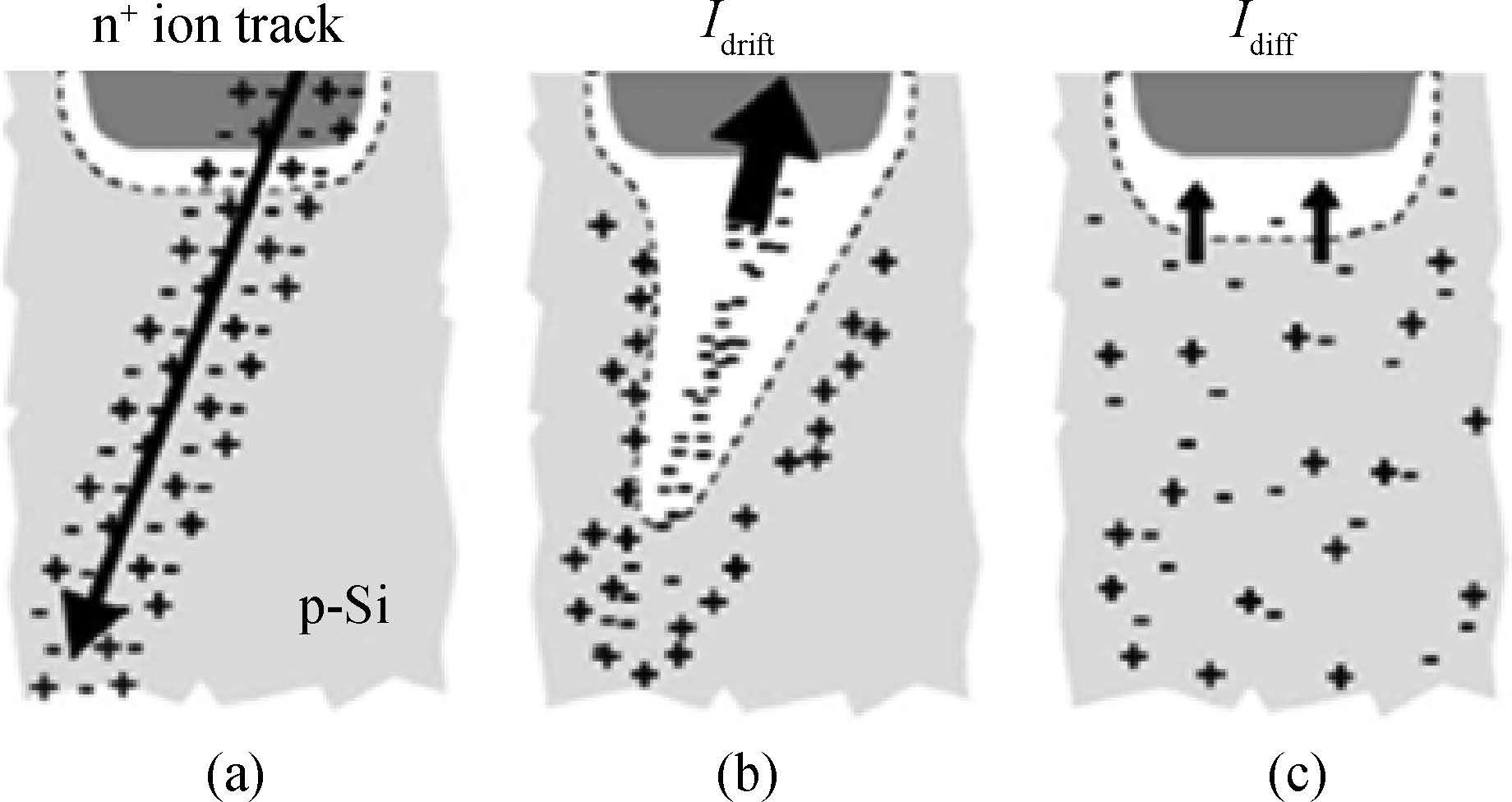
As technology feature sizes decrease, single event upset (SEU), and single event transient (SET) dominate the radiation response of microcircuits. Multiple bit upset (MBU) (or multi cell upset) effects, digital single event transient (DSET) and analogue single event transient (ASET) caused serious problems for advanced integrated circuits (ICs) applied in a radiation environment and have become a pressing issue. To face this challenge, a lot of work has been put into the single event soft error mechanism and mitigation schemes. This paper presents a review of SEU and SET, including: a brief historical overview, which summarizes the historical development of the SEU and SET study since their first observation in the 1970's; effects prominent in advanced technology, which reviews the effects such as MBU, MSET as well as SET broadening and quenching with the influence of temperature, device structure etc.; the present understanding of single event soft error mechanisms, which review the basic mechanism of single event generation including various component of charge collection; and a discussion of various SEU and SET mitigation schemes divided as circuit hardening and layout hardening that could help the designer meet his goals.


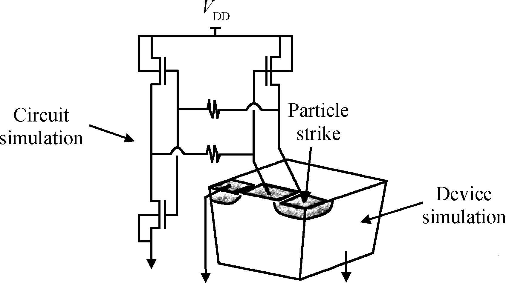
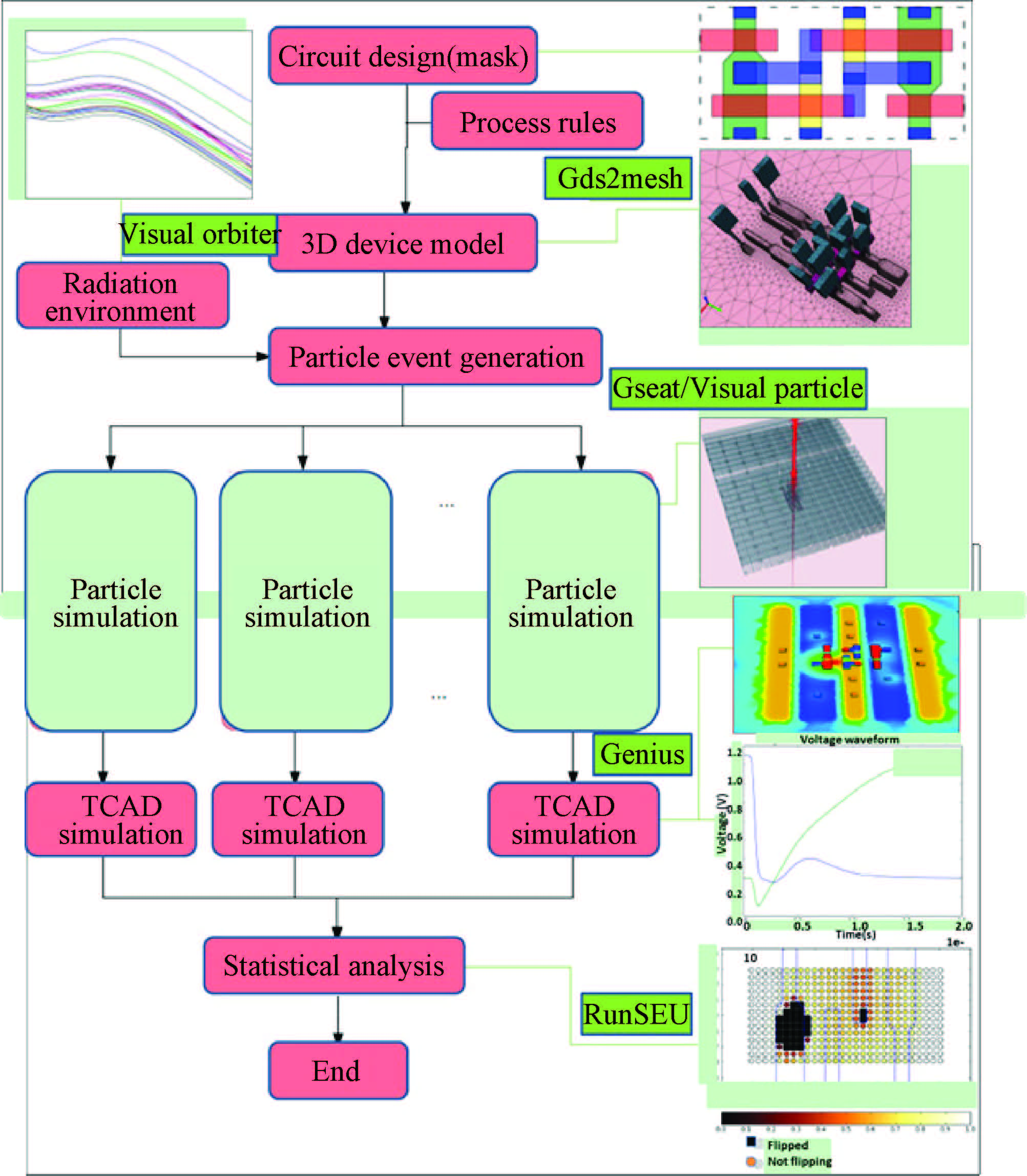
This paper reviews the status of research in modeling and simulation of single-event effects (SEE) in digital devices and integrated circuits. After introducing a brief historical overview of SEE simulation, different level simulation approaches of SEE are detailed, including material-level physical simulation where two primary methods by which ionizing radiation releases charge in a semiconductor device (direct ionization and indirect ionization) are introduced, device-level simulation where the main emerging physical phenomena affecting nanometer devices (bipolar transistor effect, charge sharing effect) and the methods envisaged for taking them into account are focused on, and circuit-level simulation where the methods for predicting single-event response about the production and propagation of single-event transients (SETs) in sequential and combinatorial logic are detailed, as well as the soft error rate trends with scaling are particularly addressed.

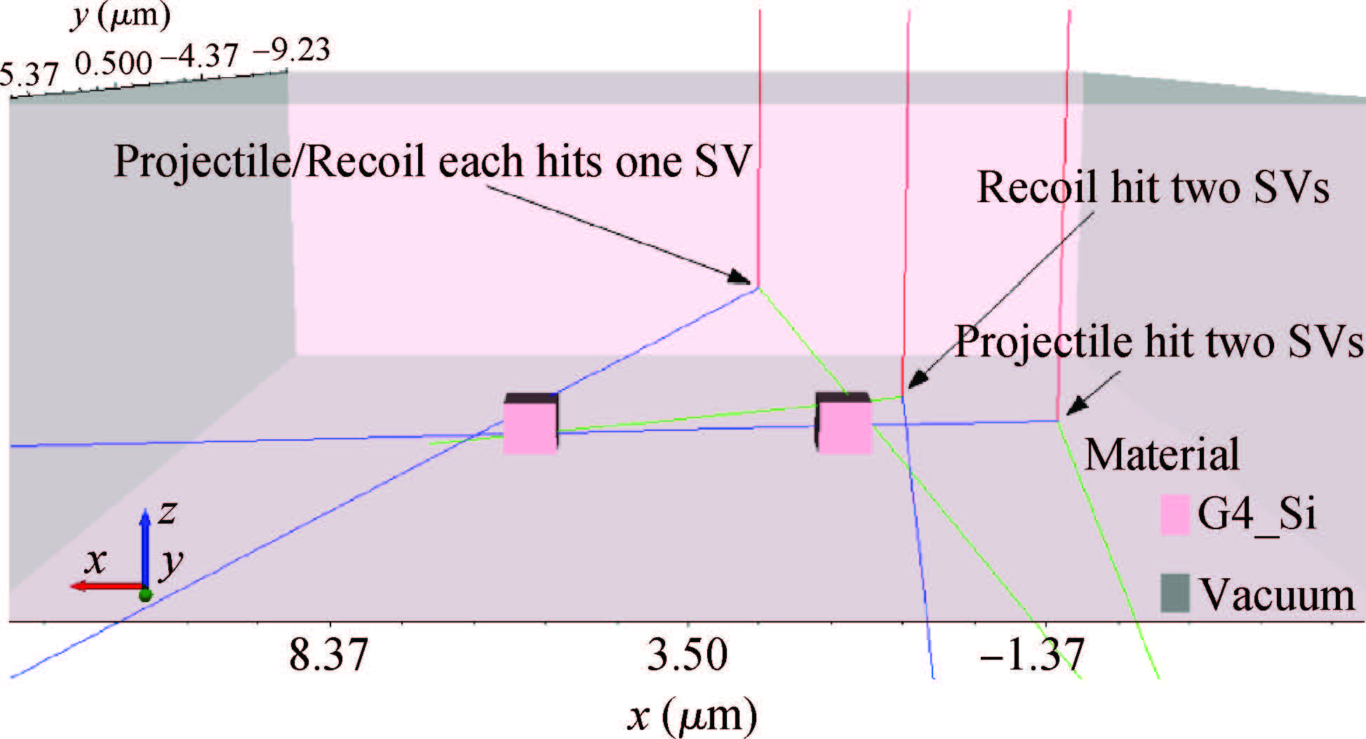


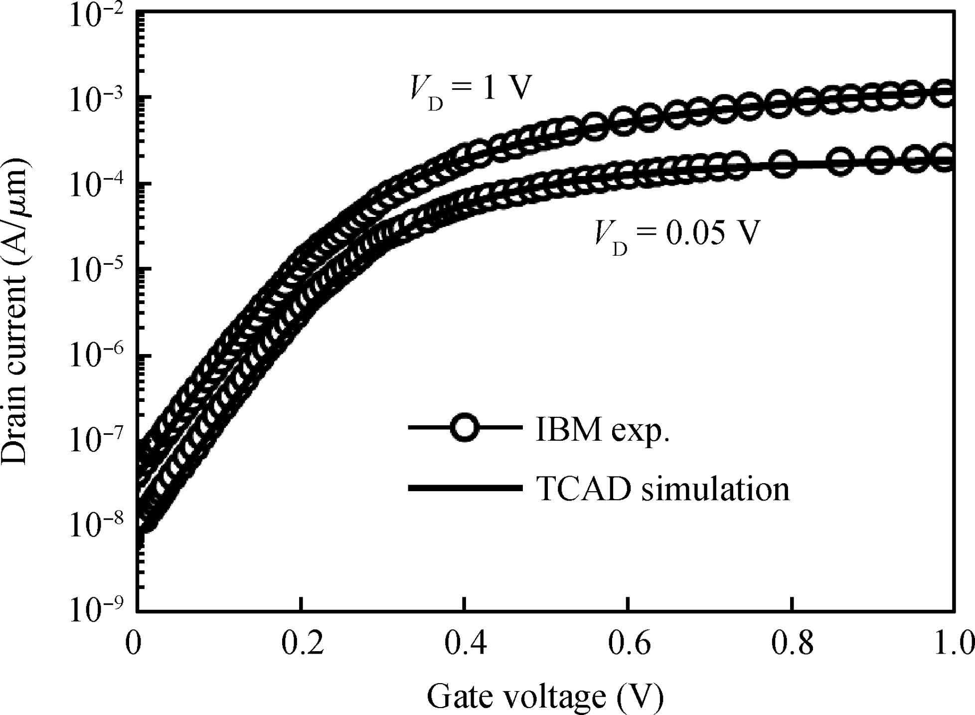
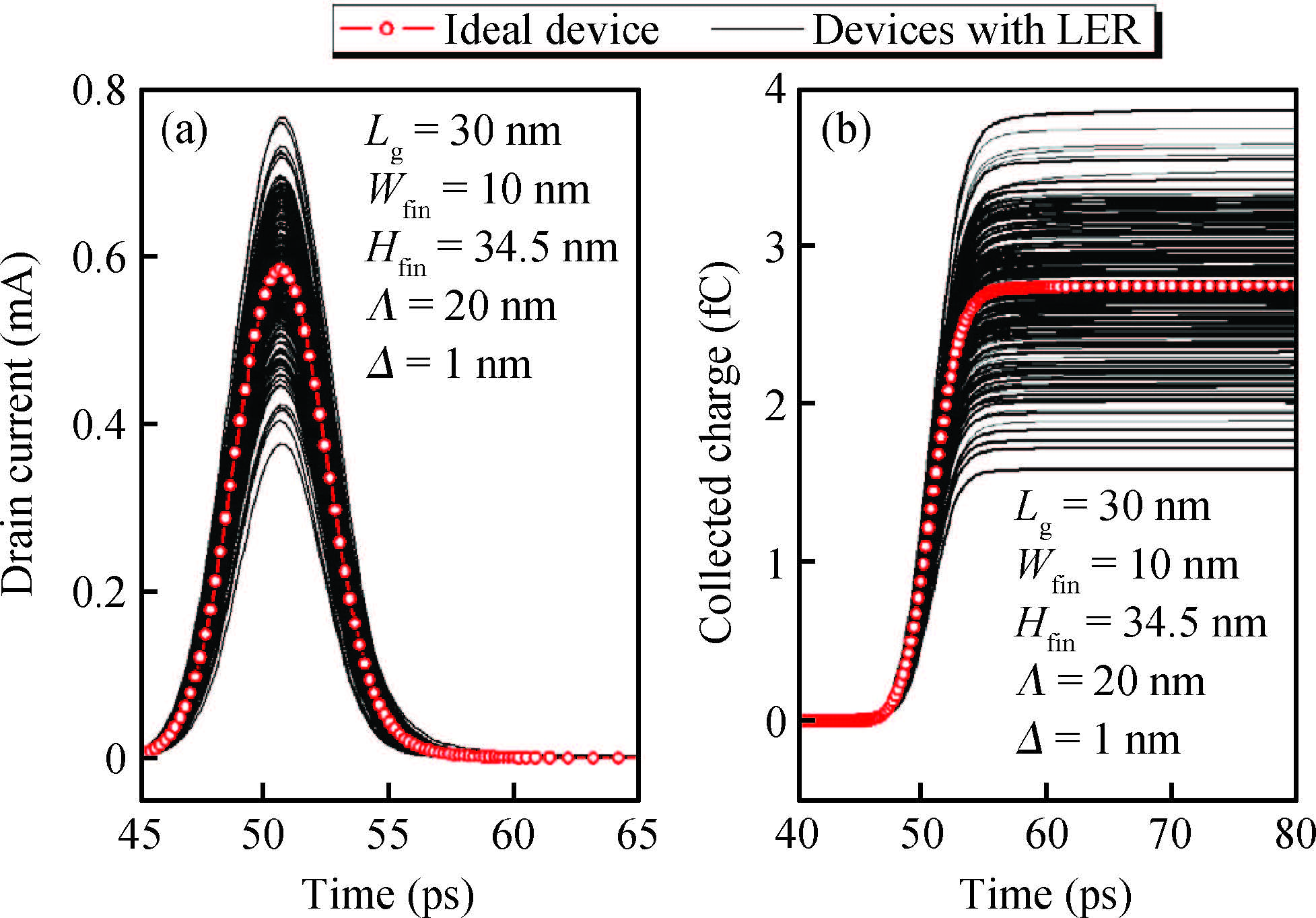
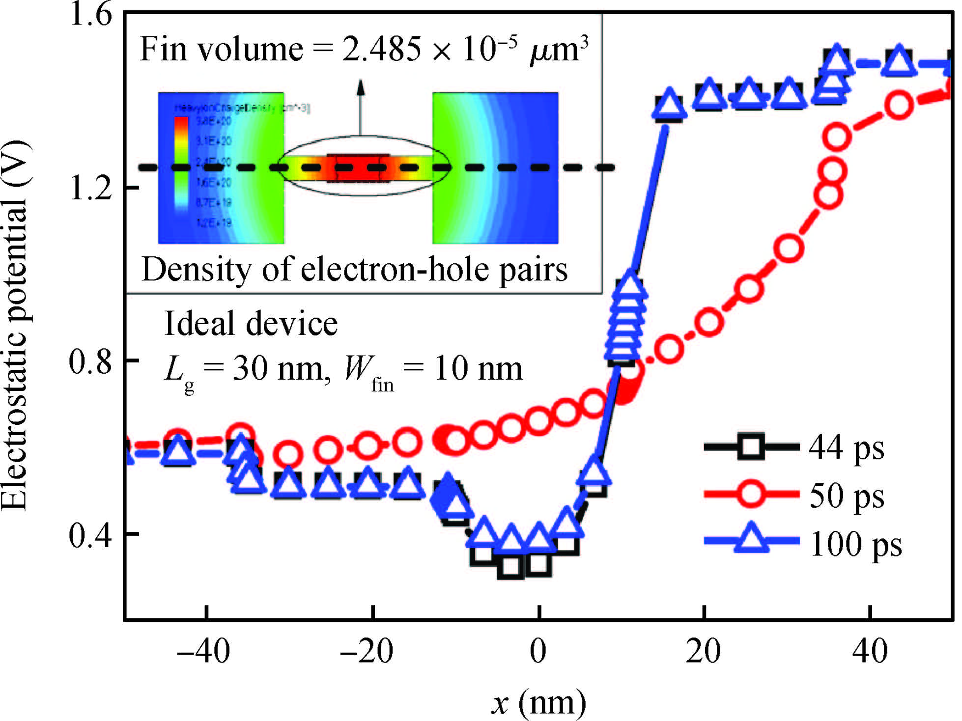
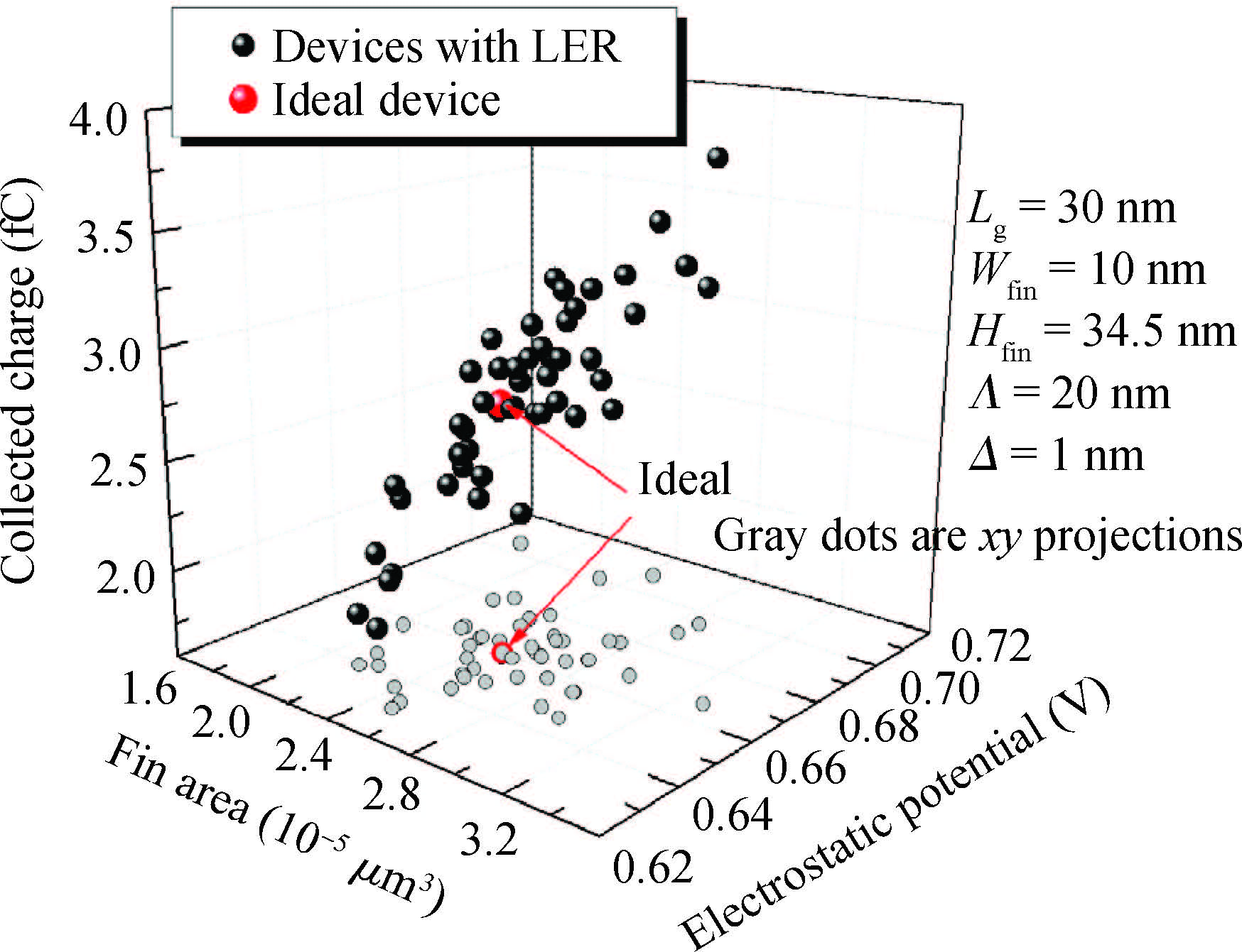
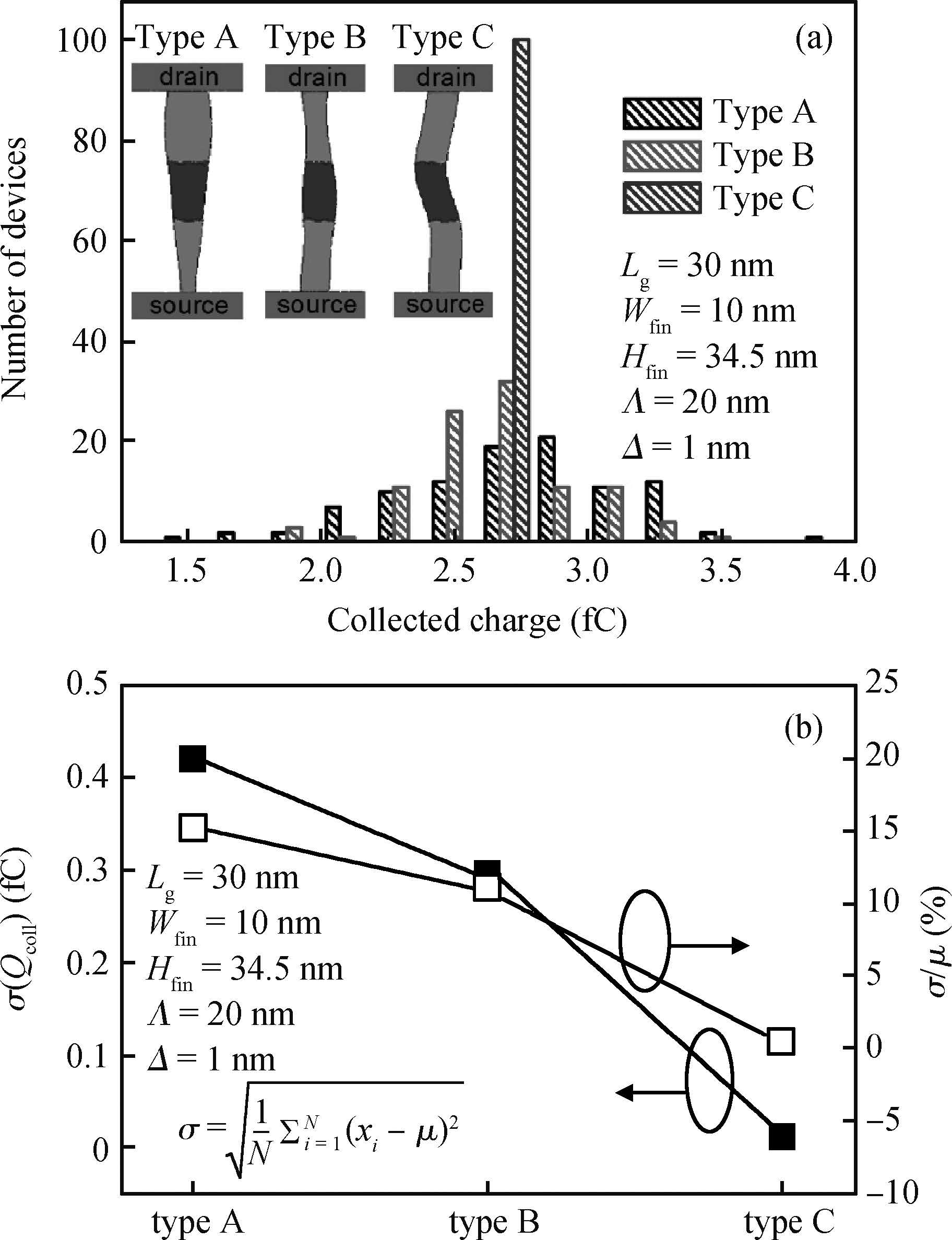
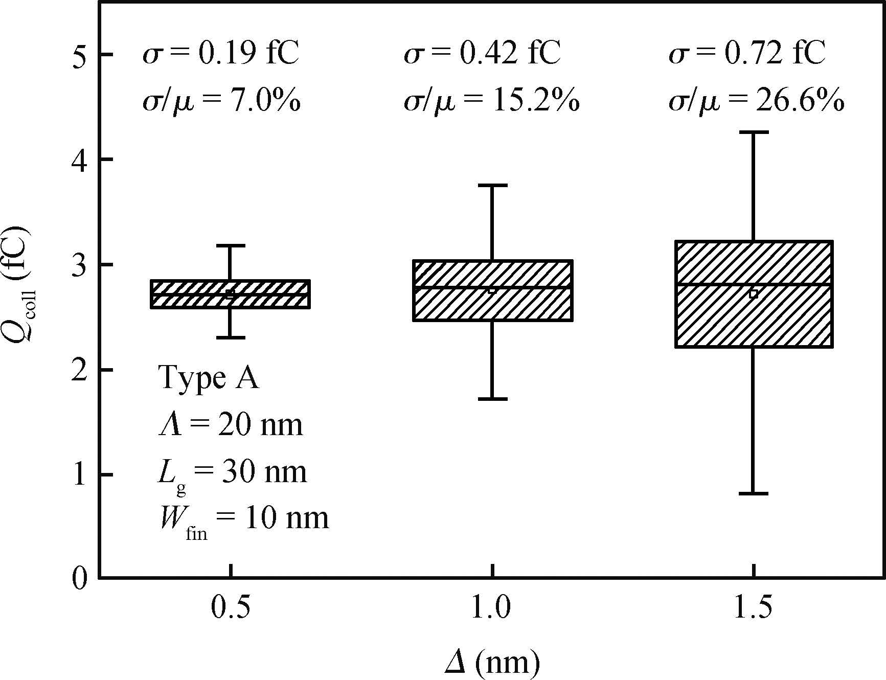
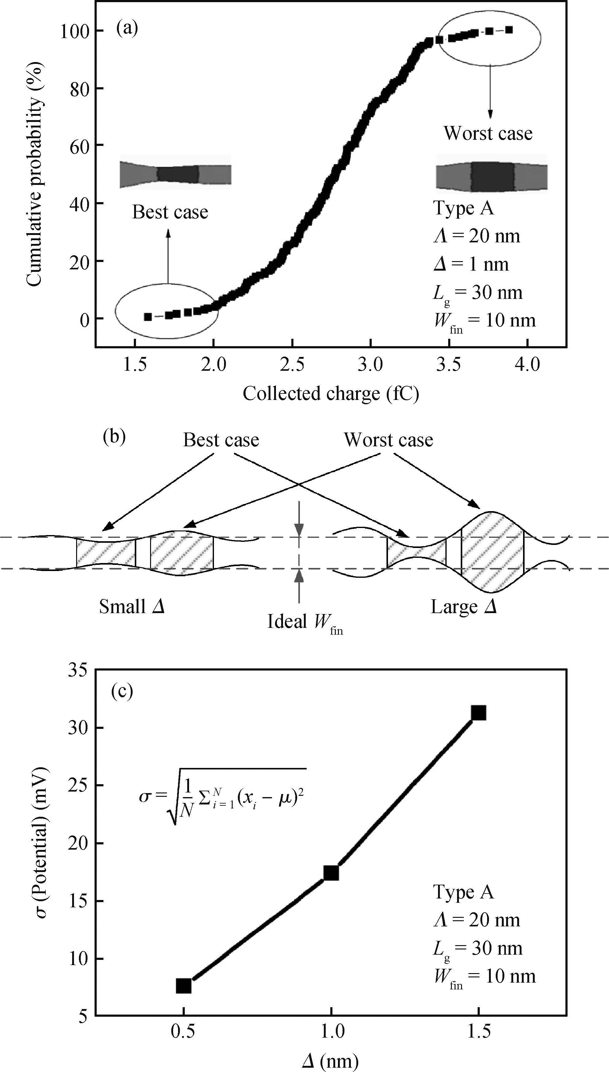
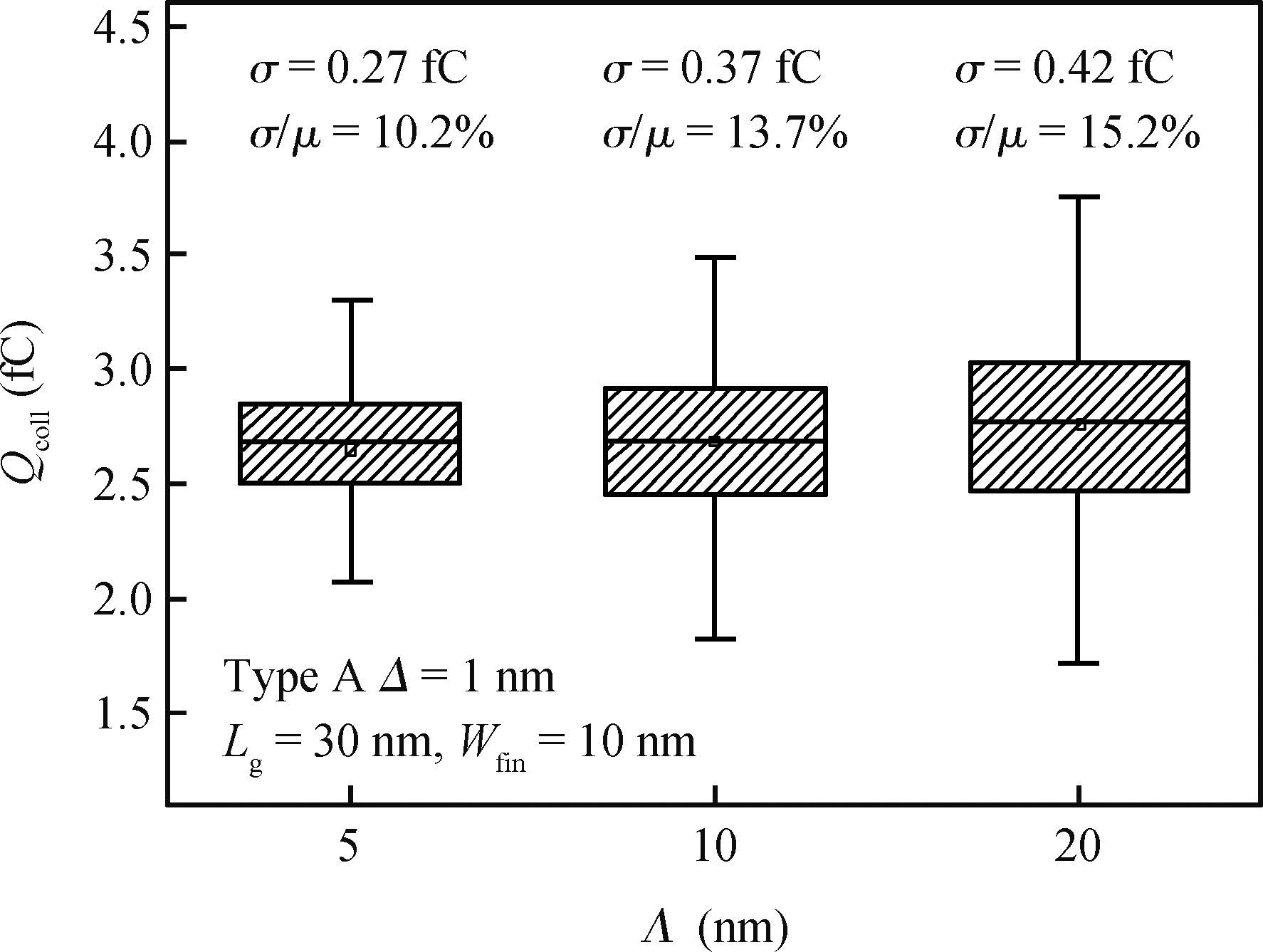
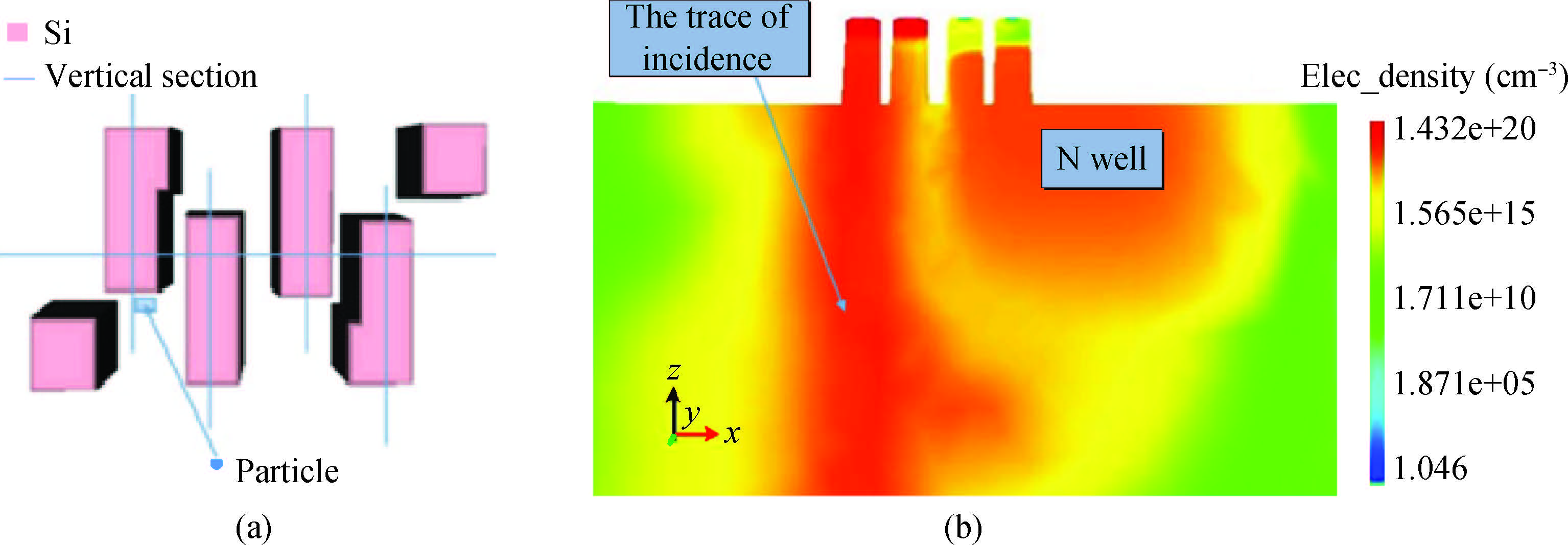
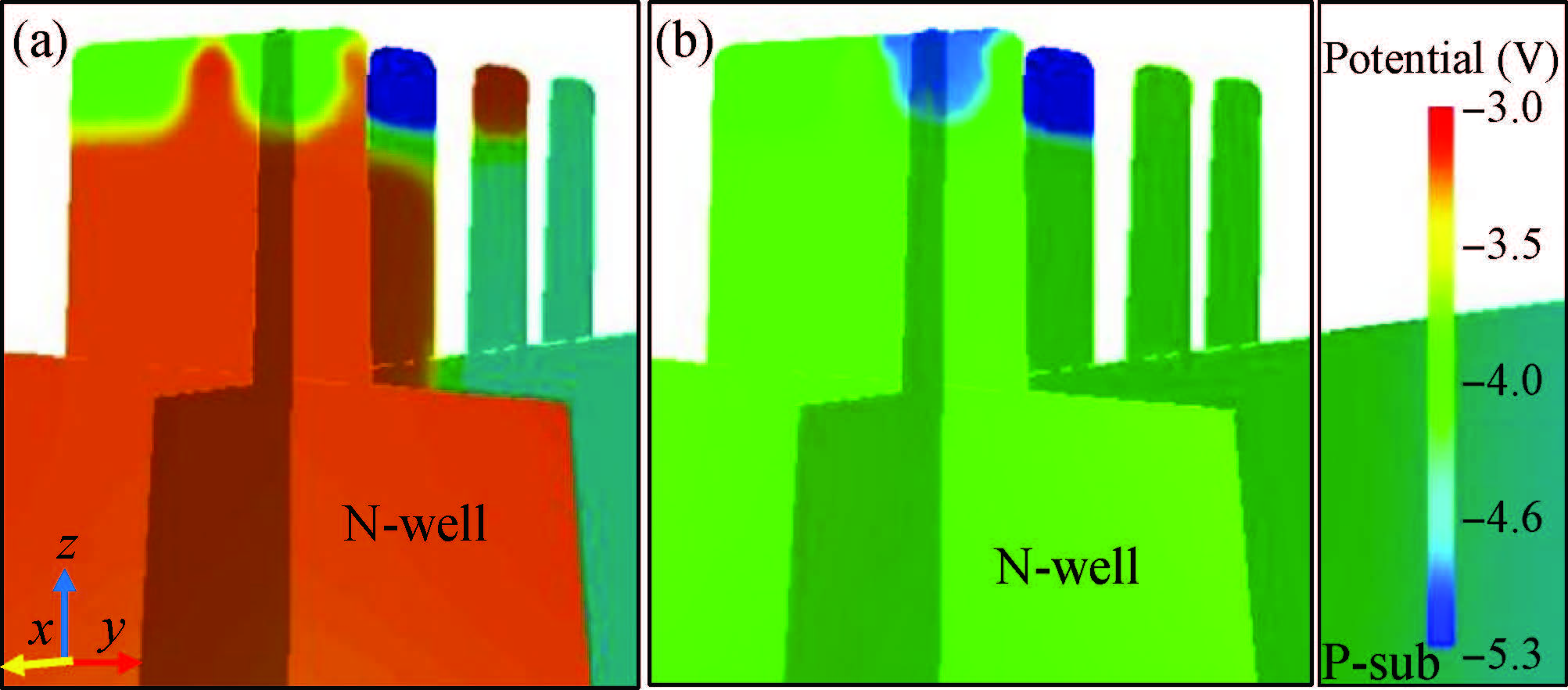
The impact of process induced variation on the response of SOI FinFET to heavy ion irradiation is studied through 3-D TCAD simulation for the first time. When FinFET biased at OFF state configuration (Vgs=0, Vds=Vdd) is struck by a heavy ion, the drain collects ionizing charges under the electric field and a current pulse (single event transient, SET) is consequently formed. The results reveal that with the presence of line-edge roughness (LER), which is one of the major variation sources in nano-scale FinFETs, the device-to-device variation in terms of SET is observed. In this study, three types of LER are considered: type A has symmetric fin edges, type B has irrelevant fin edges and type C has parallel fin edges. The results show that type A devices have the largest SET variation while type C devices have the smallest variation. Further, the impact of the two main LER parameters, correlation length and root mean square amplitude, on SET variation is discussed as well. The results indicate that variation may be a concern in radiation effects with the down scaling of feature size.


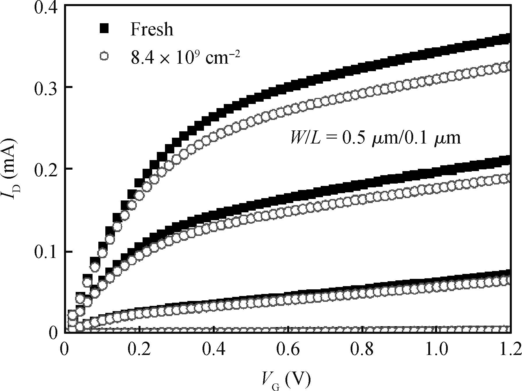
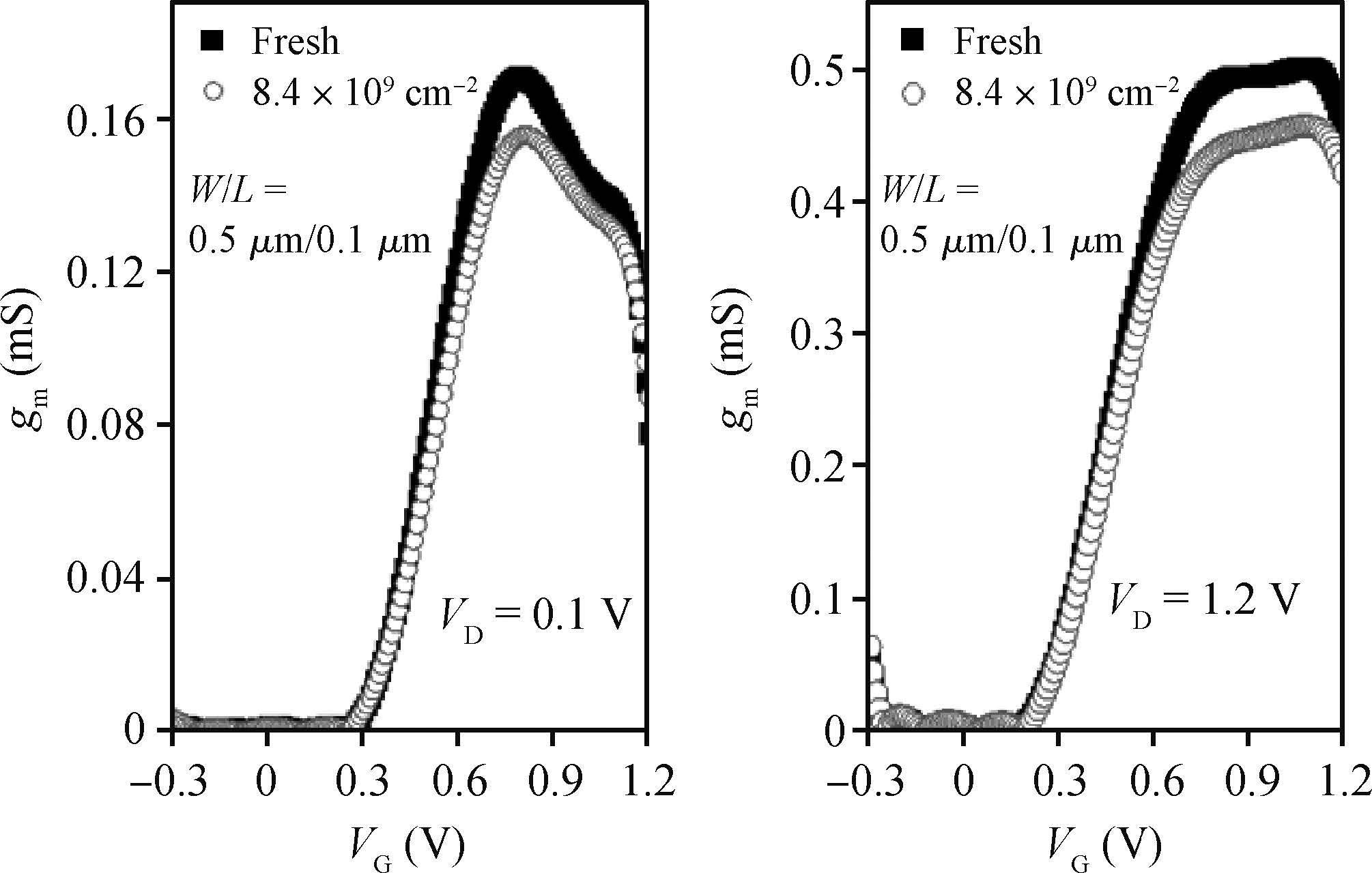
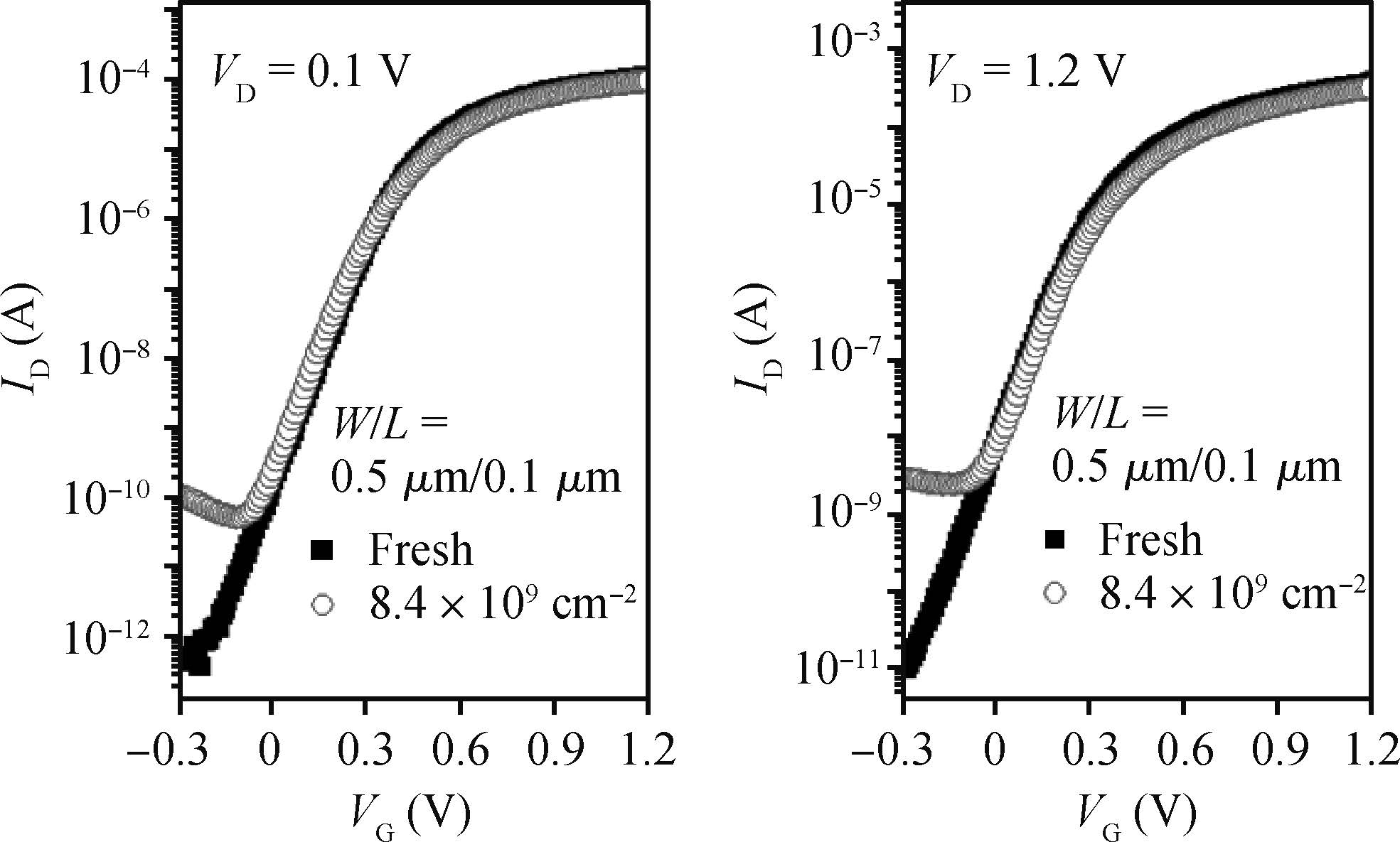
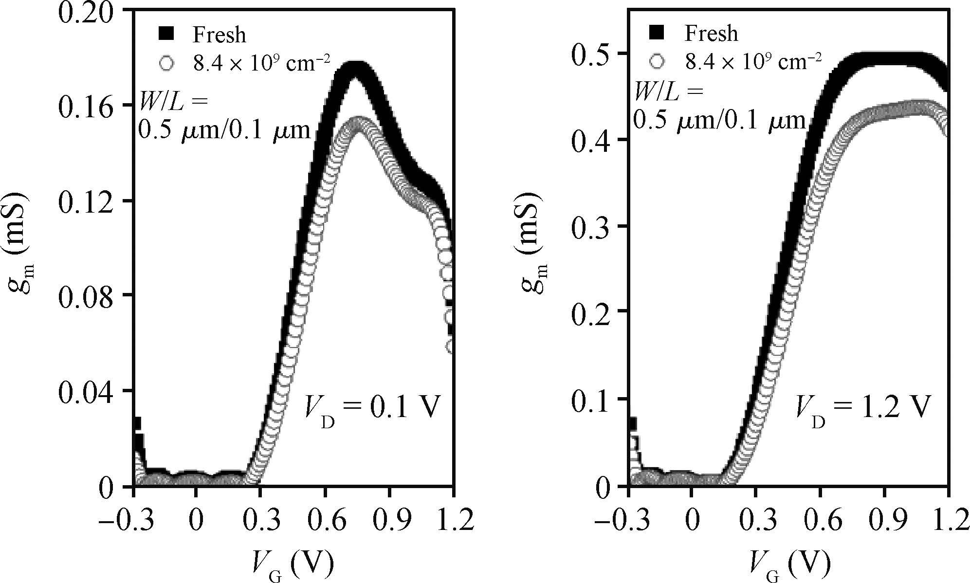
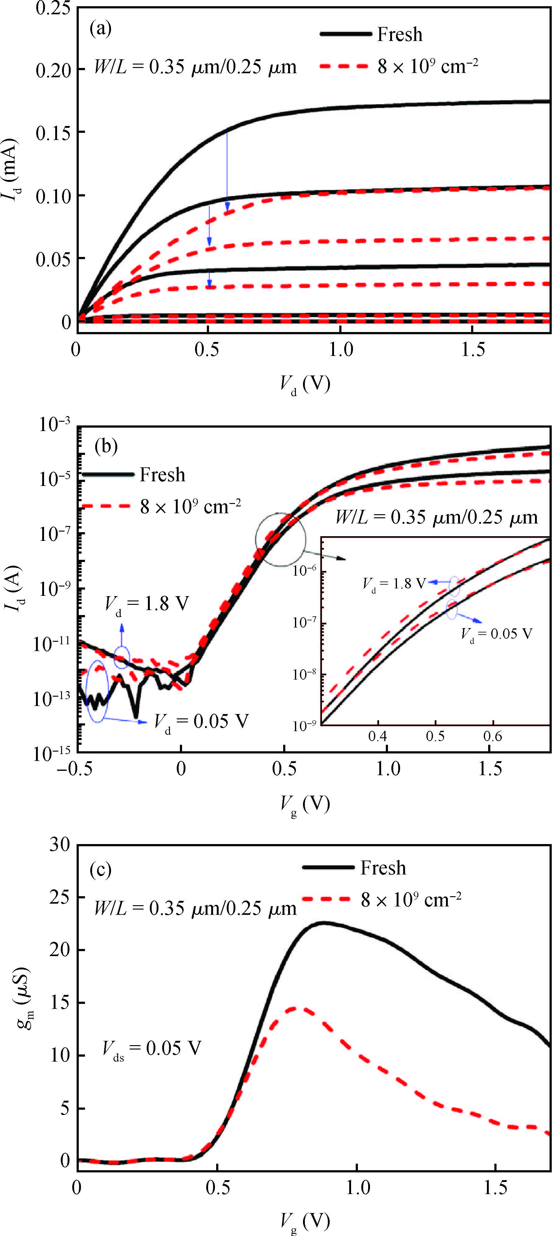
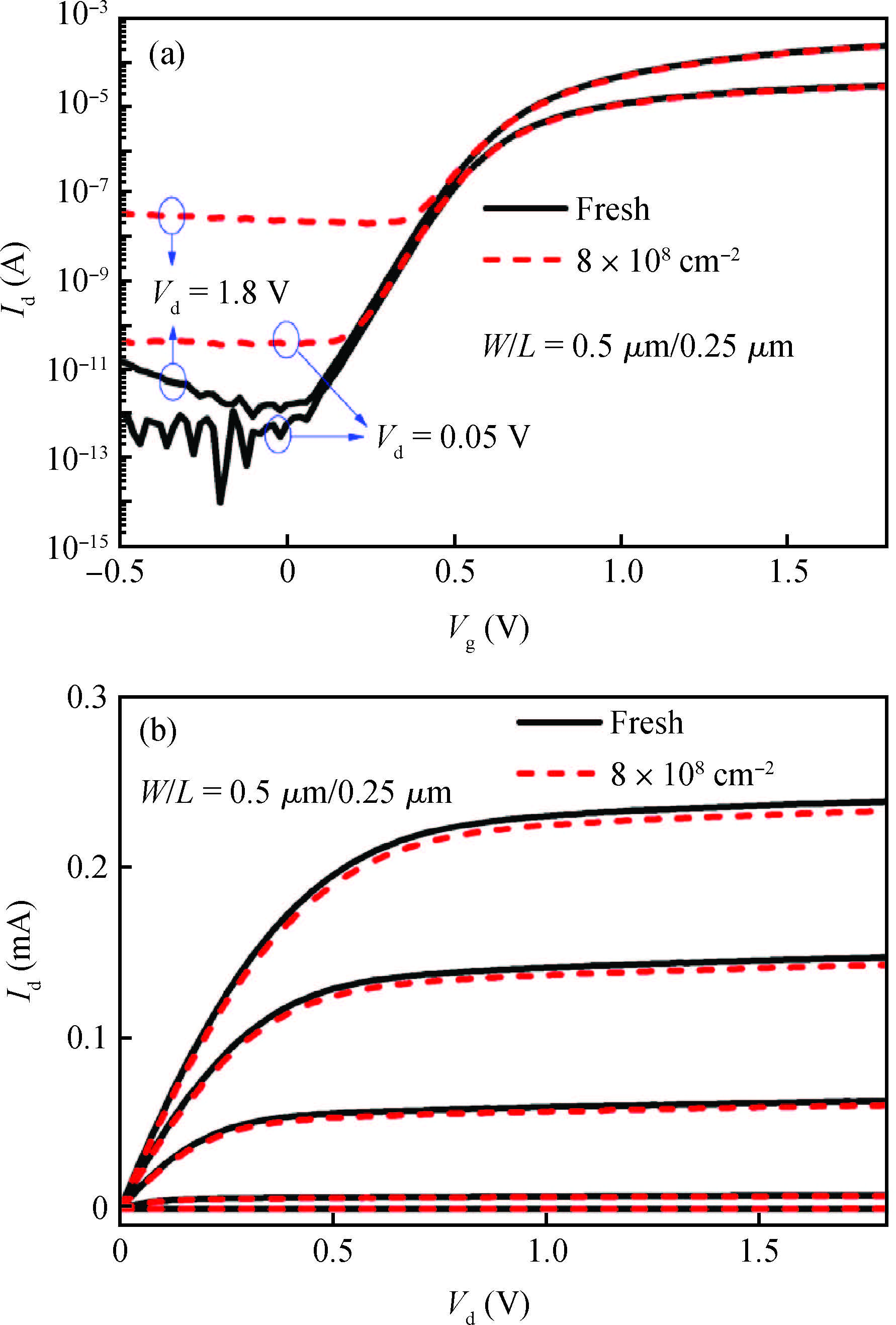
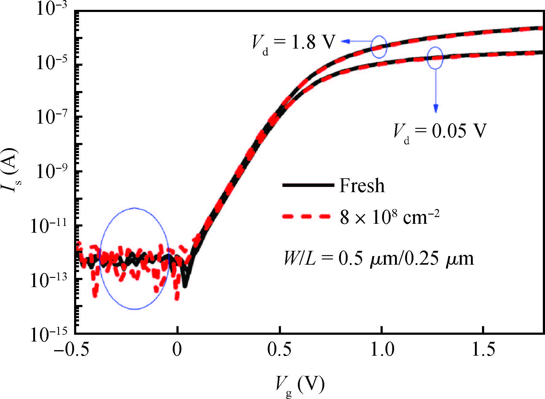
The radiation response of 90 nm bulk silicon MOS devices after heavy ion irradiation is experimentally investigated. Due to the random strike of the incident particle, different degradation behaviors of bulk silicon MOS devices are observed. The drain current and maximum transconductance degrade as a result of the displacement damage in the channel induced by heavy ion strike. The off-state leakage current degradation and threshold voltage shift are also observed after heavy ion irradiation. The results suggest that the radiation induced damage of sub-100 nm MOS devices caused by heavy ion irradiation should be paid attention.


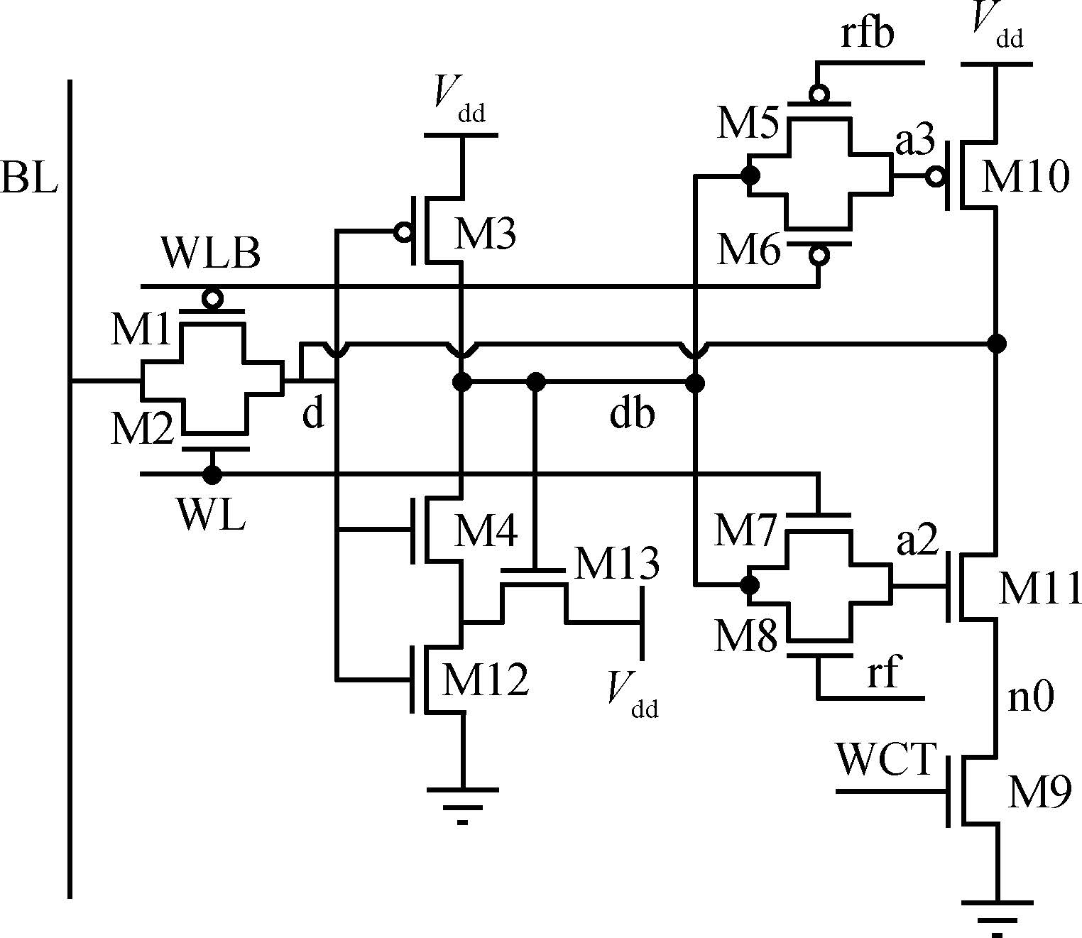
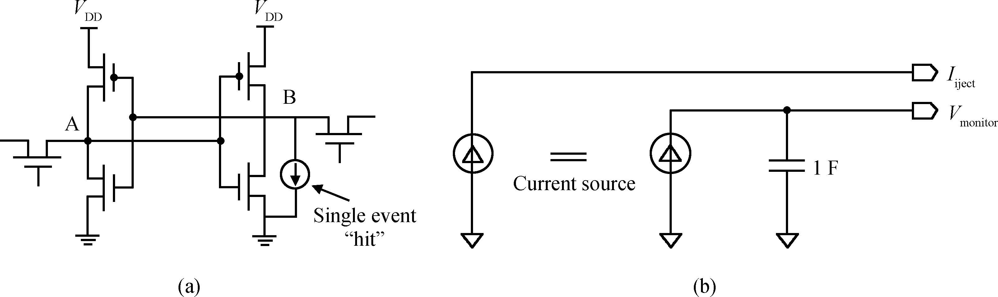
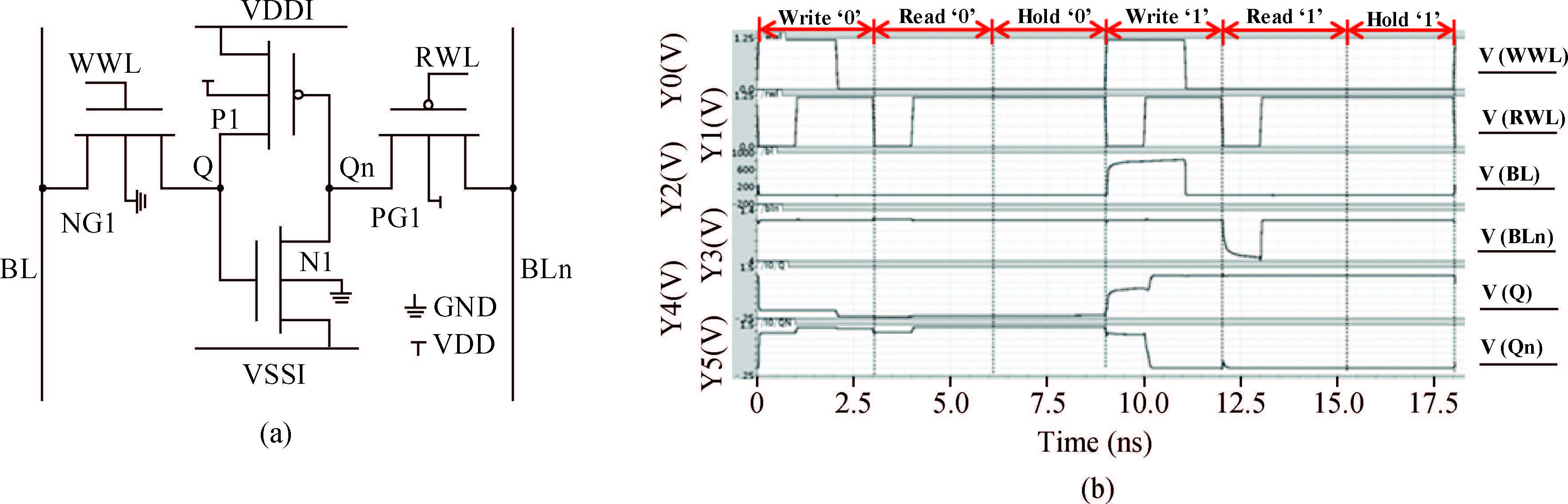
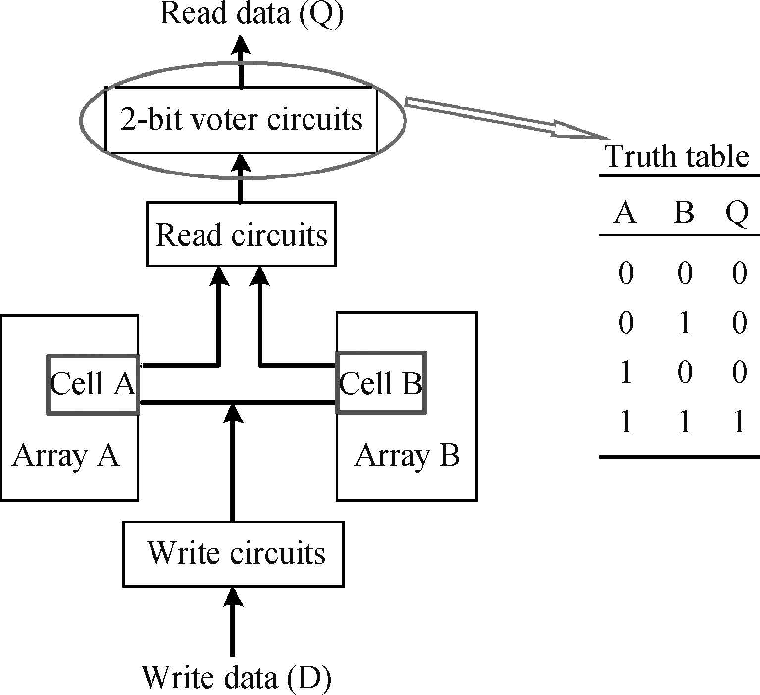
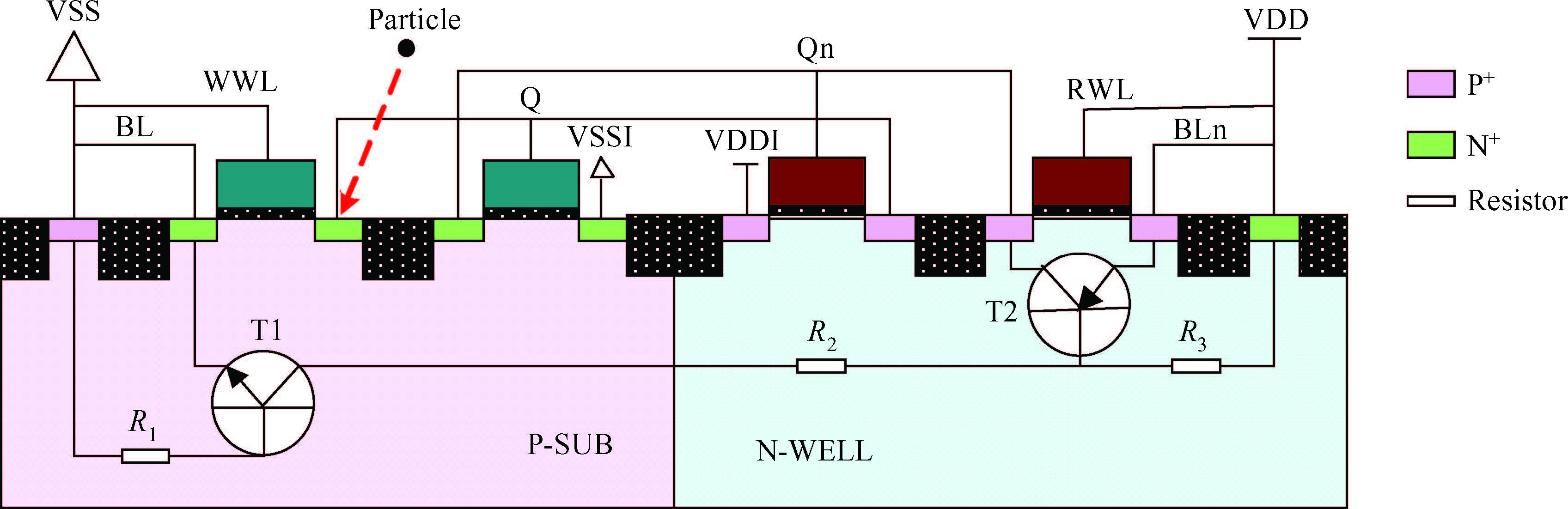
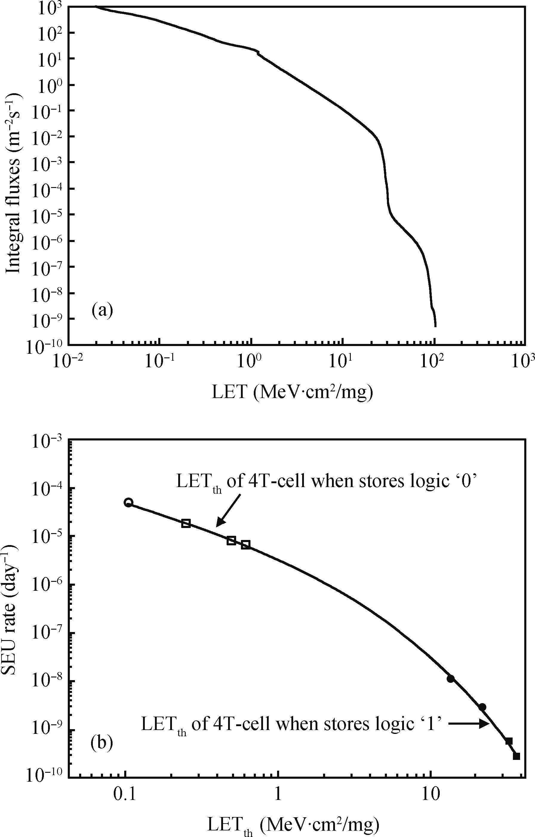
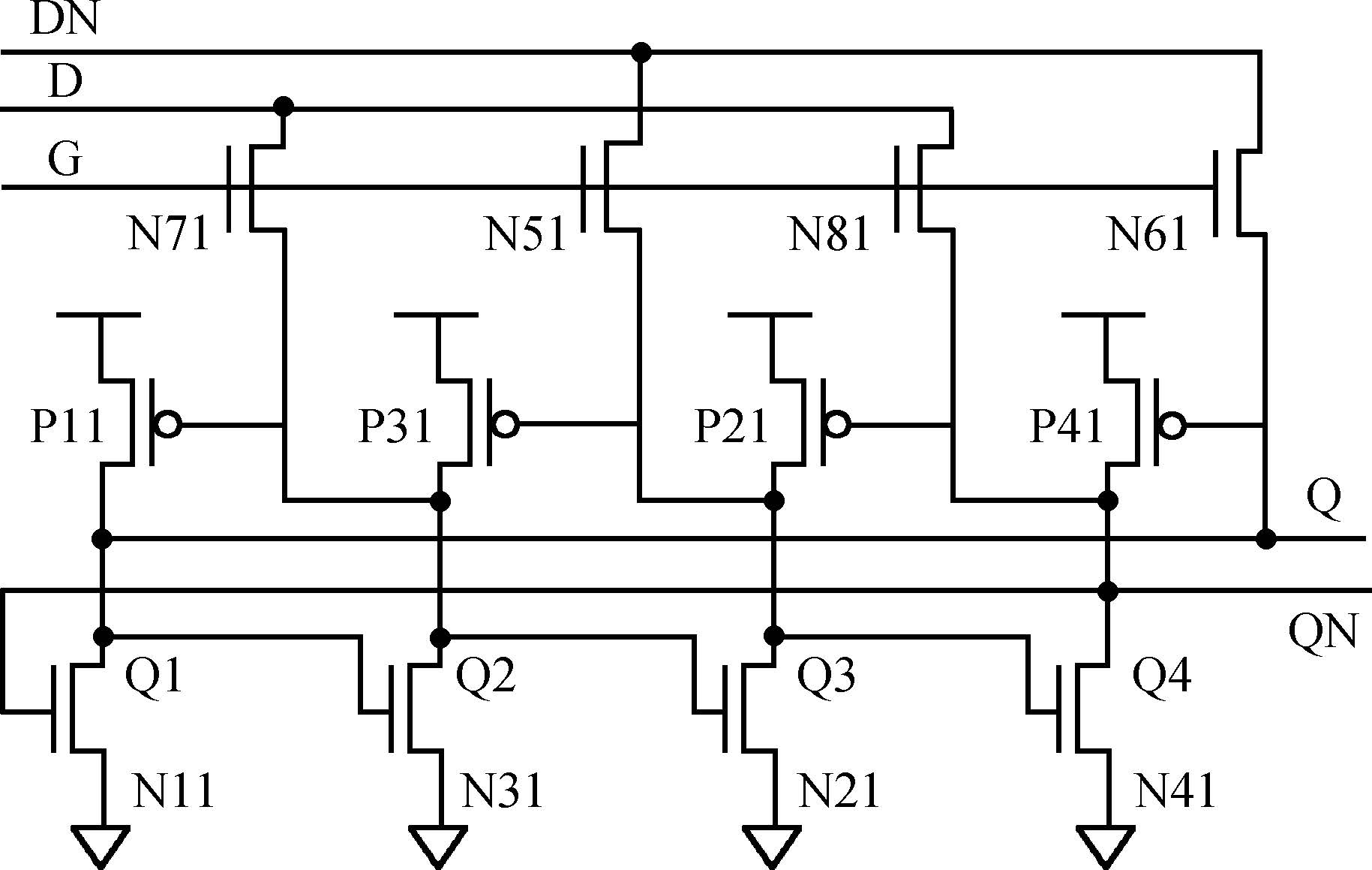
A novel 4T-cell based duplication redundancy SRAM is proposed for SEU radiation hardening applications. The memory cell is designed with a 65-nm low leakage process; the operation principle and the SEU radiation hardening mechanism are discussed in detail. The SEE characteristics and failure mechanism are also studied with a 3-D device simulator. The results show that the proposed SRAM structure exhibits high SEU hardening performance with a small cell size.

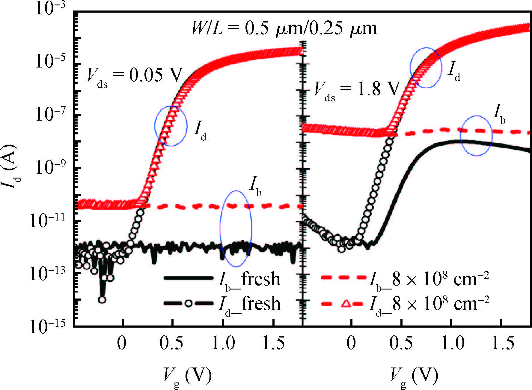
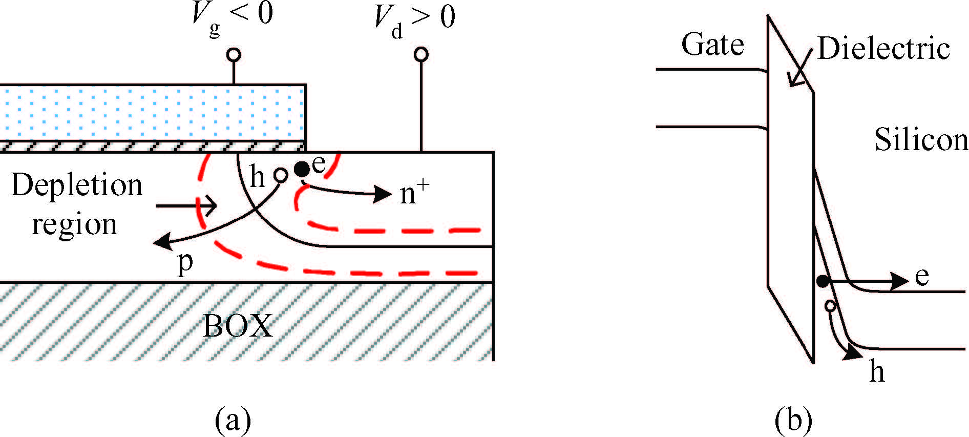
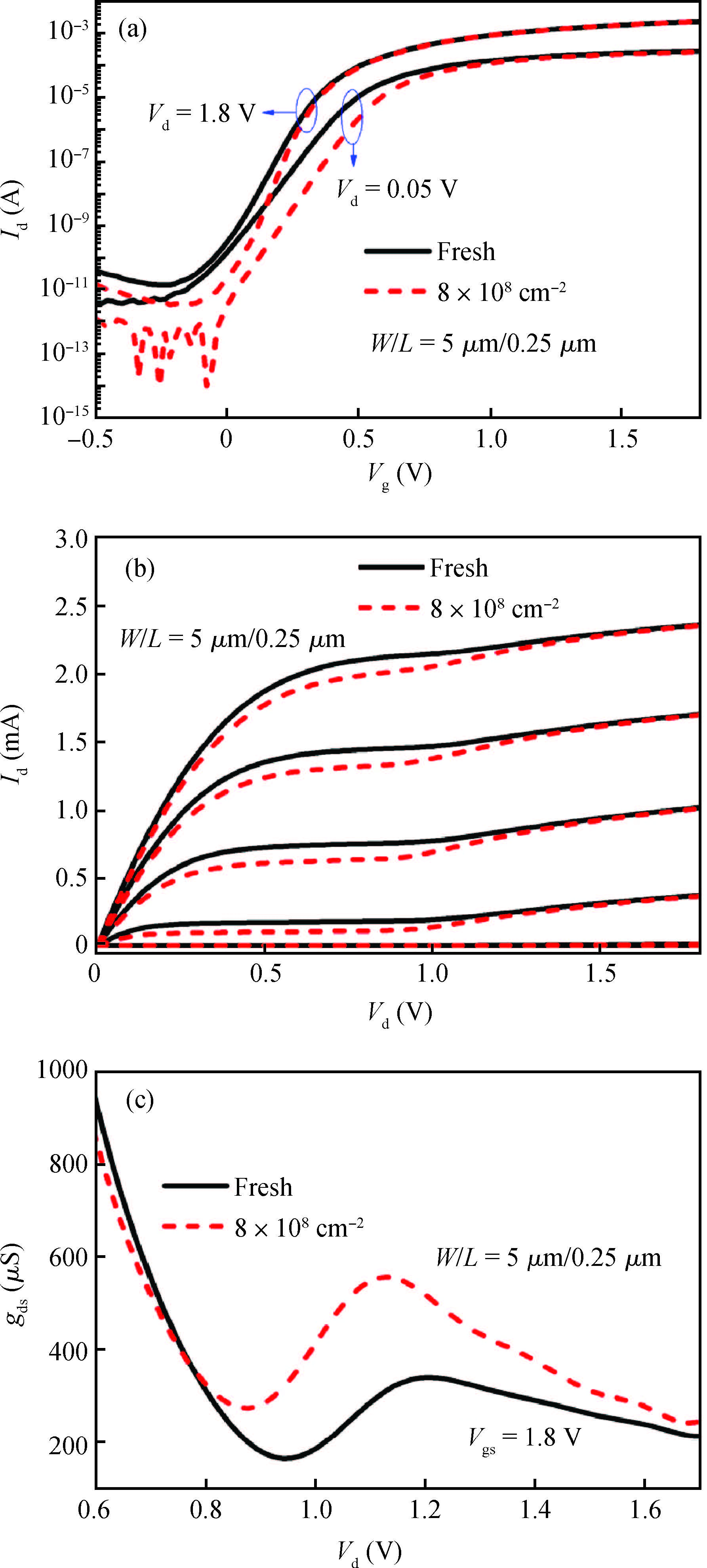
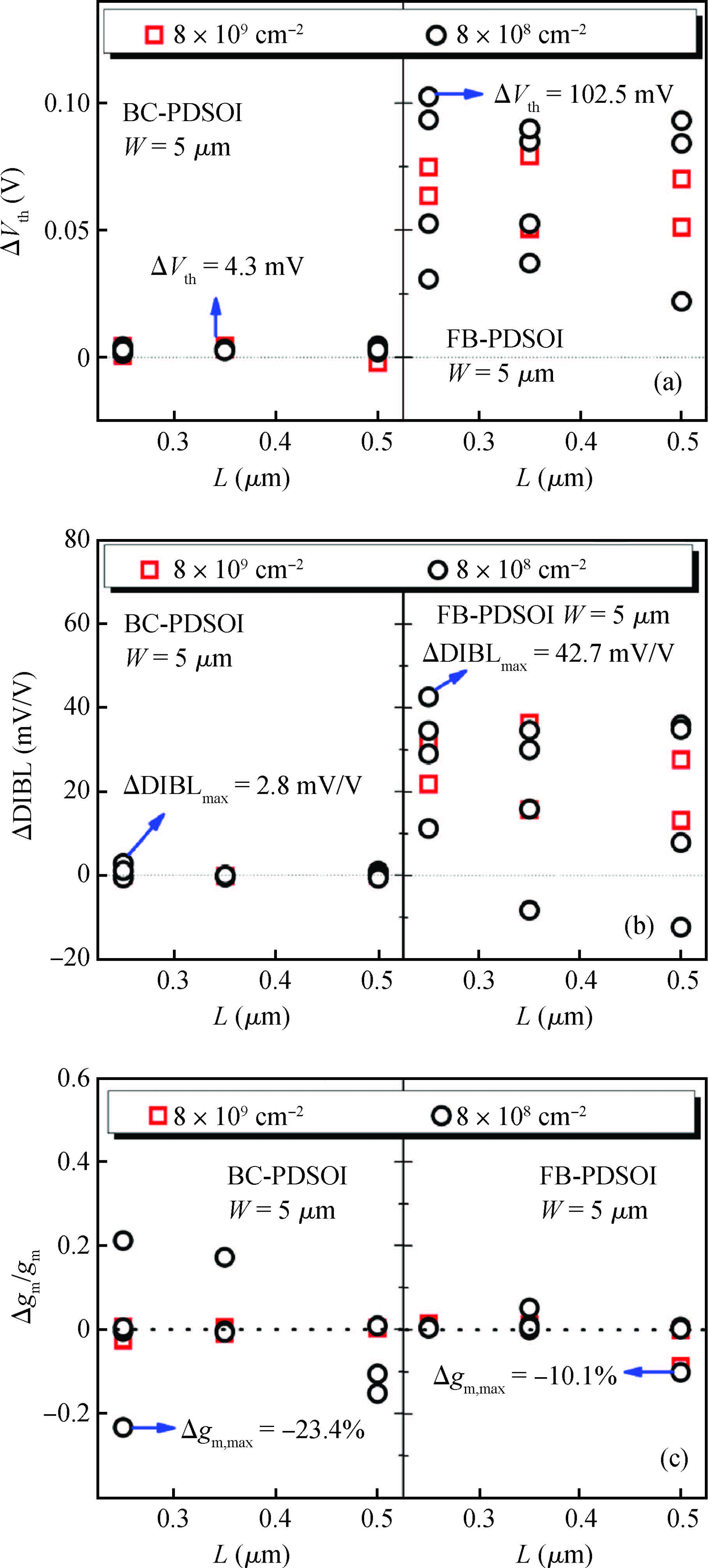
The effects of the physical damages induced by heavy ion irradiation on the performance of partially-depleted SOI devices are experimentally investigated. After heavy ion exposure, different degradation phenomena are observed due to the random strike of heavy ions. A decrease of the saturation current and transconductance, and an enhanced gate-induced drain leakage current are observed, which are mainly attributed to the displacement damages that may be located in the channel, the depletion region of the drain/body junction or the gate-to-drain overlap region. Further, PDSOI devices with and without body contact are compared, which reveals the differences in the threshold voltage shift, the drain-induced barrier lowing effect, the transconductance and the kink effect. The results may provide a guideline for radiation hardened design.


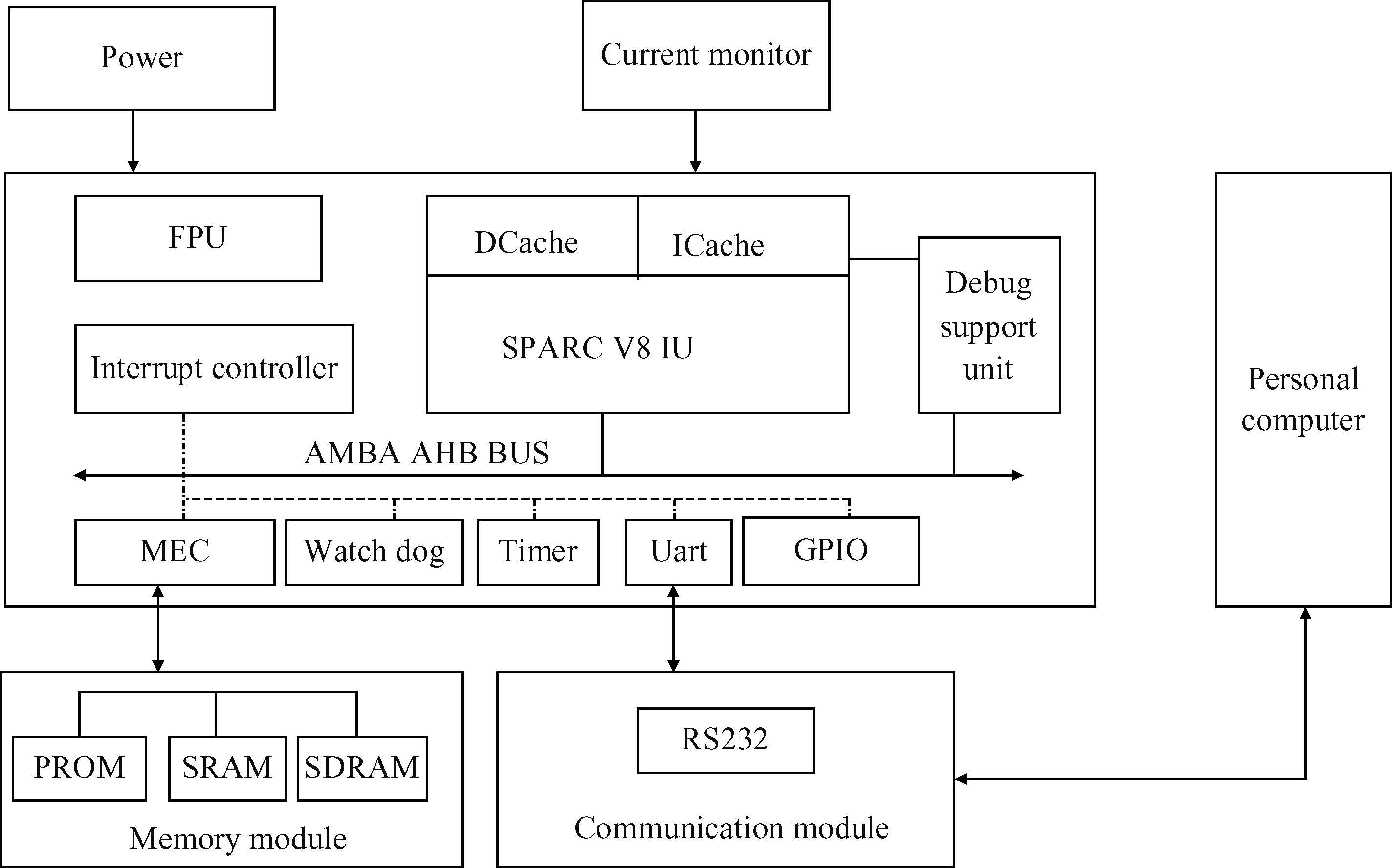
Design of a highly reliable SPARC-V8 processor for space applications requires consideration single-event effects including single event upsets, single event transients, single event latch-up, as well as cumulative effects such as the total ionizing dose (TID). In this paper, the fault tolerance of the SPARC-V8 processor to radiation effects is discussed in detail. The SPARC-V8 processor, fabricated in the 65 nm CMOS process, achieves a frequency of 300 MHz with a core area of 9.78×9.78 mm2, and it is demonstrated that its radiation hardened performance is suitable for operating in a space environment through the key elements' experiments, which show TID resistance to 300 krad(Si), SEL immunity to greater than 92.5 MeV·cm2/mg, and an SEU error rate of 2.51×10⁻⁴ per day.


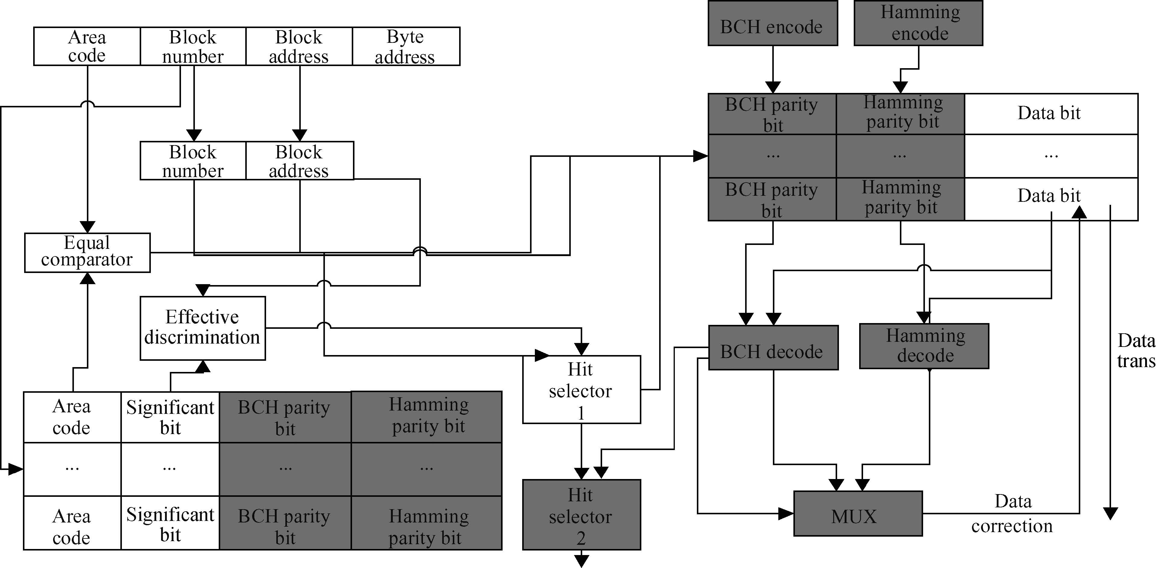
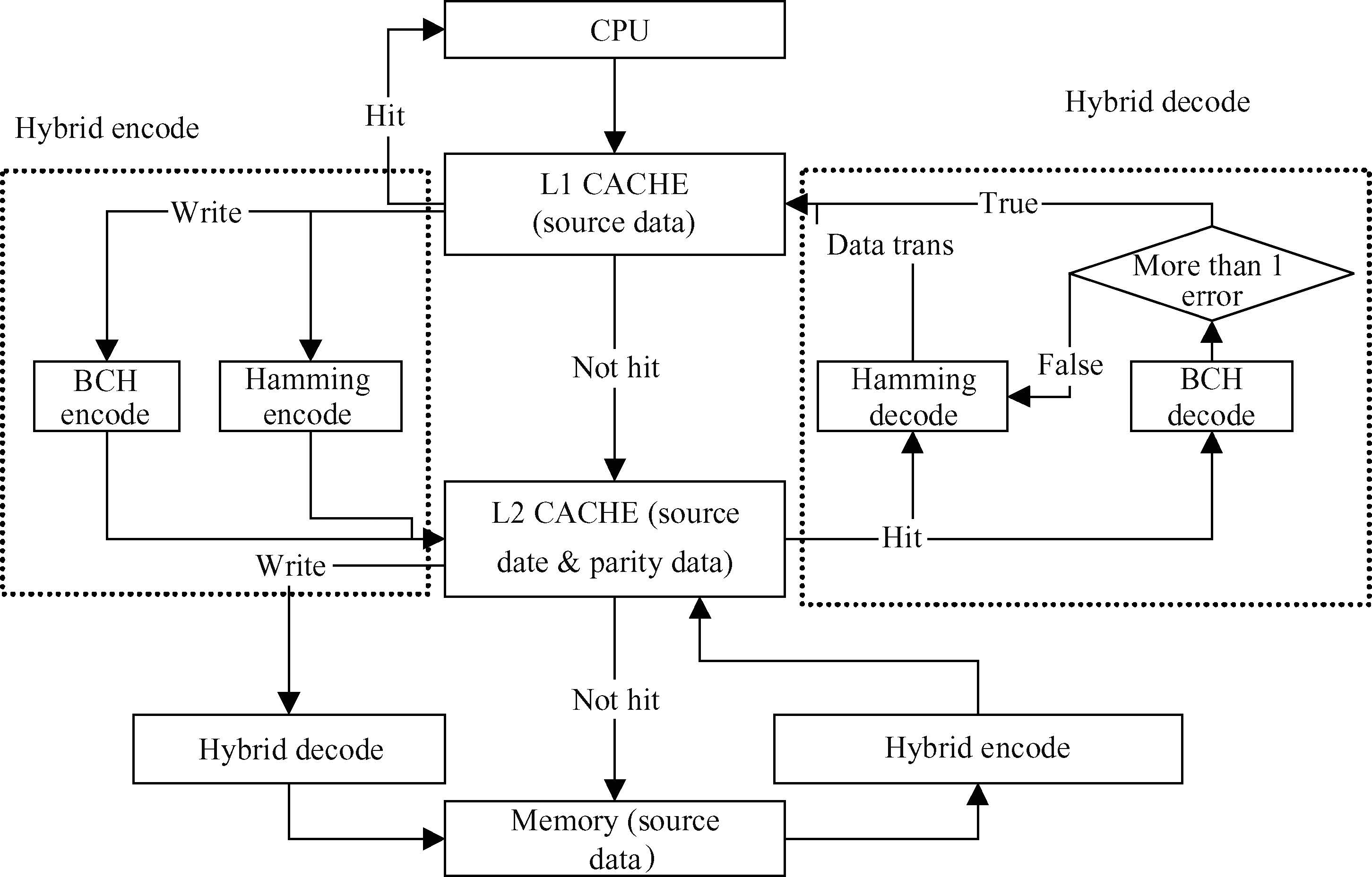
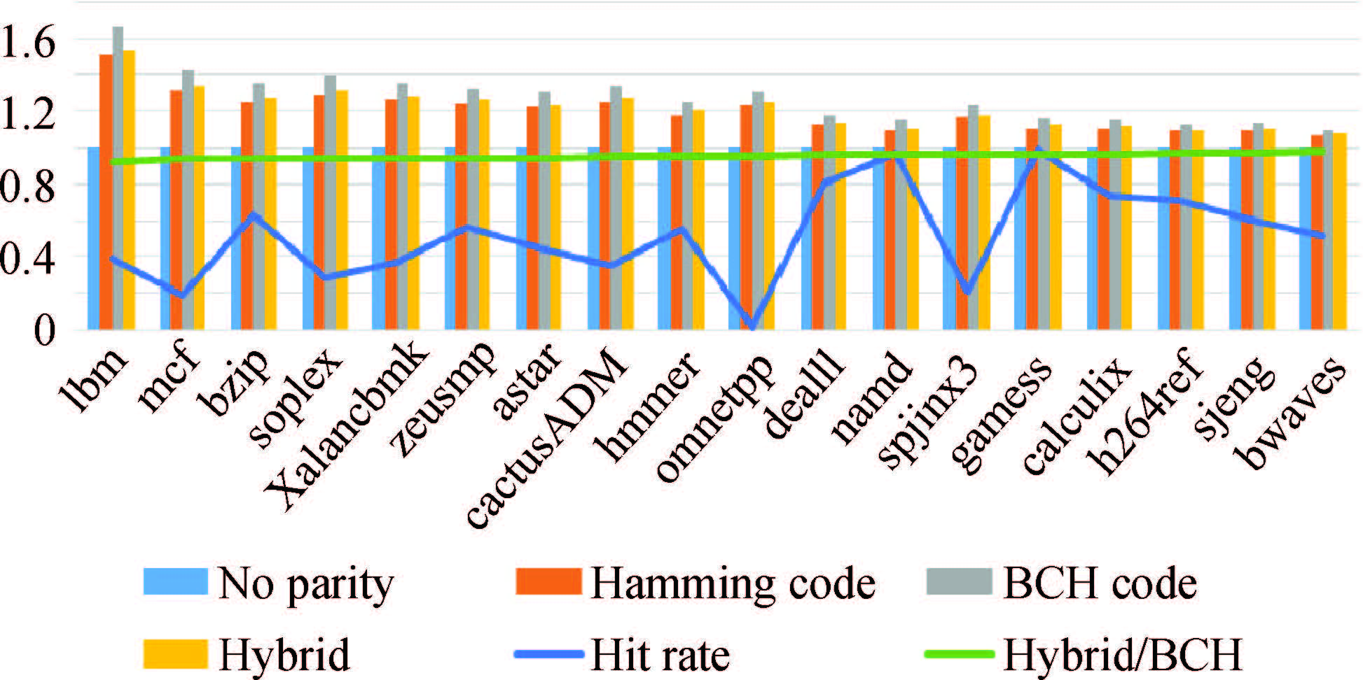
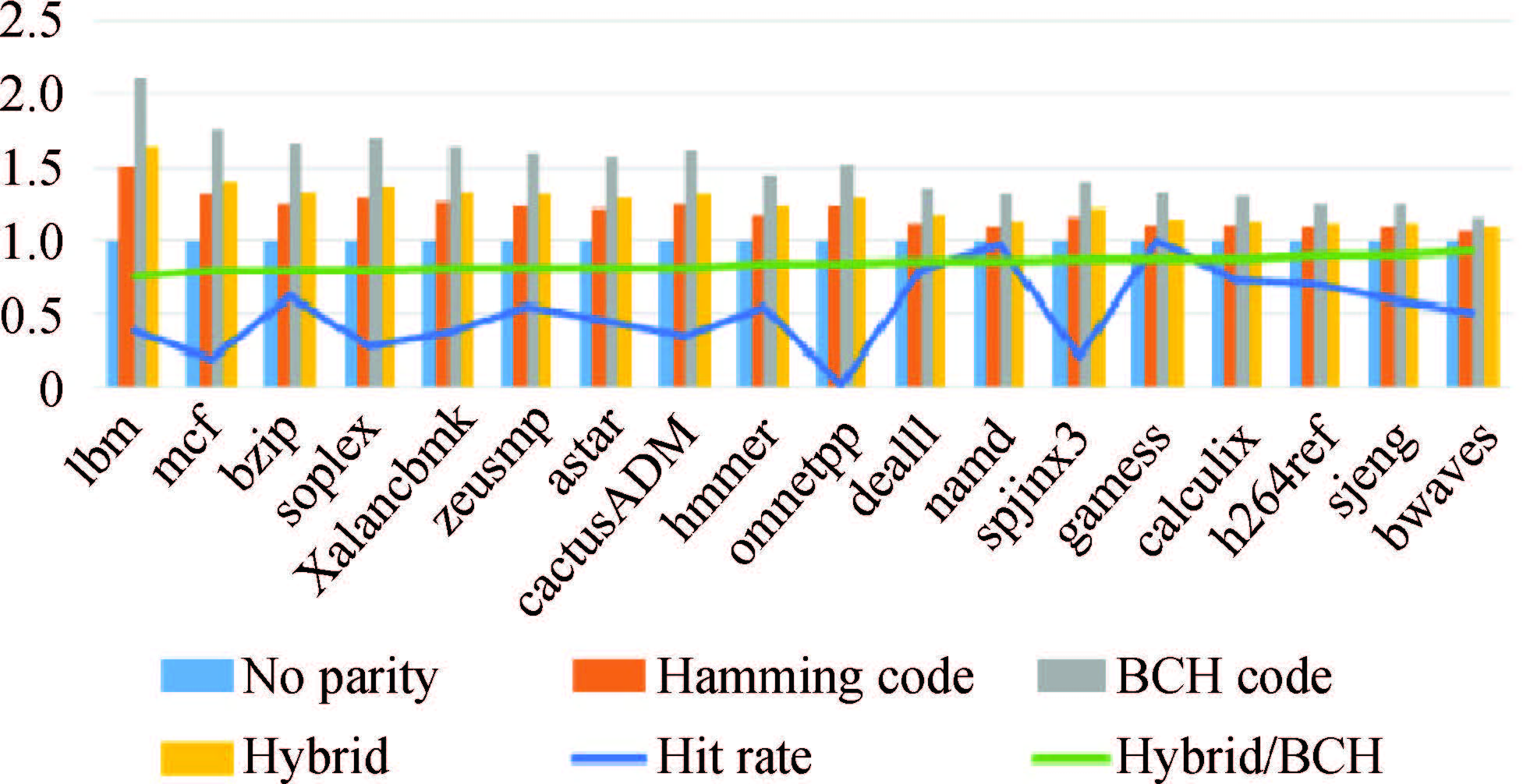
For the processor working in the radiation environment in space, it tends to suffer from the single event effect on circuits and system failures, due to cosmic rays and high energy particle radiation. Therefore, the reliability of the processor has become an increasingly serious issue. The BCH-based error correction code can correct multi-bit errors, but it introduces large latency overhead. This paper proposes a hybrid error correction approach that combines BCH and EDAC to correct both multi-bit and single-bit errors for caches with low cost. The proposed technique can correct up to four-bit error, and correct single-bit error in one cycle. Evaluation results show that, the proposed hybrid error-correction scheme can improve the performance of cache accesses up to 20% compared to the pure BCH scheme.

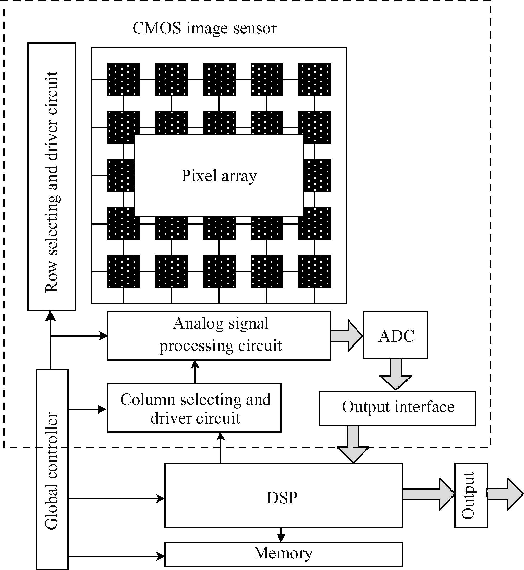
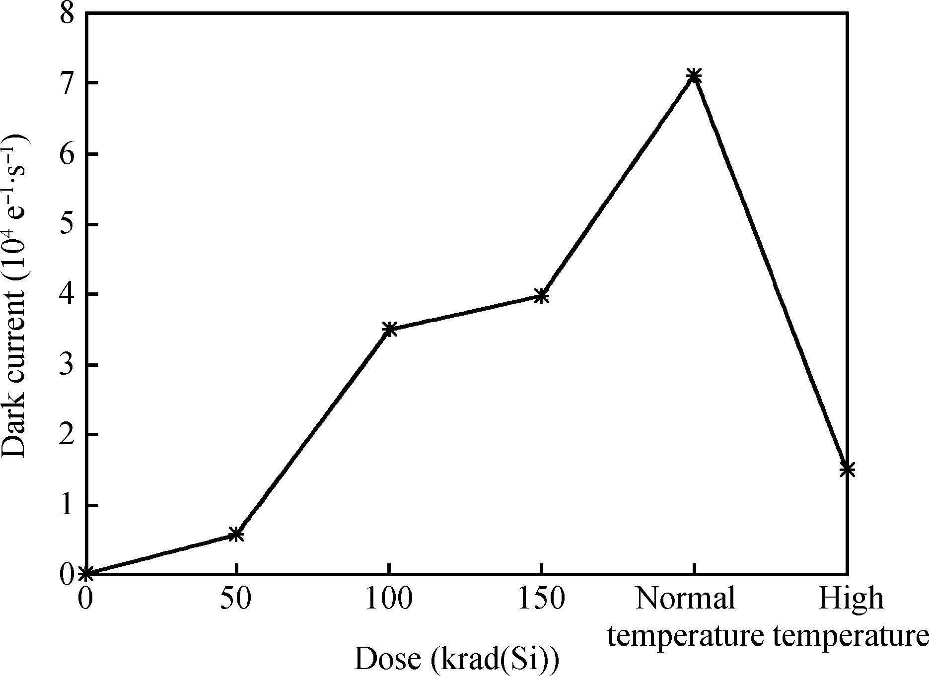
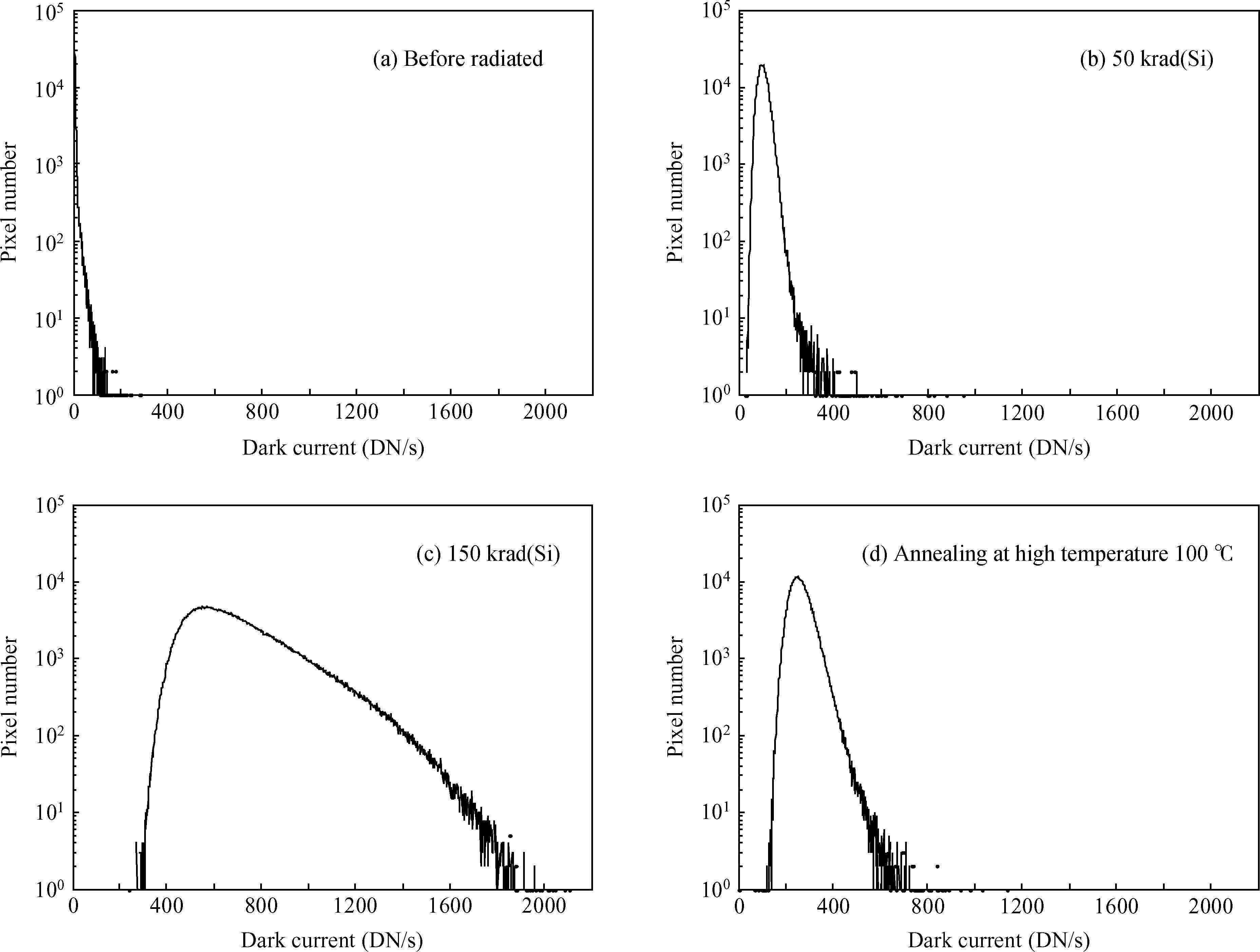
A systemic solution for radiation hardened design is presented. Besides, a series of experiments have been carried out on the samples, and then the photoelectric response characteristic and spectral characteristic before and after the experiments have been comprehensively analyzed. The performance of the CMOS image sensor with the radiation hardened design technique realized total-dose resilience up to 300 krad(Si) and resilience to single-event latch up for LET up to110 MeV·cm2/mg.


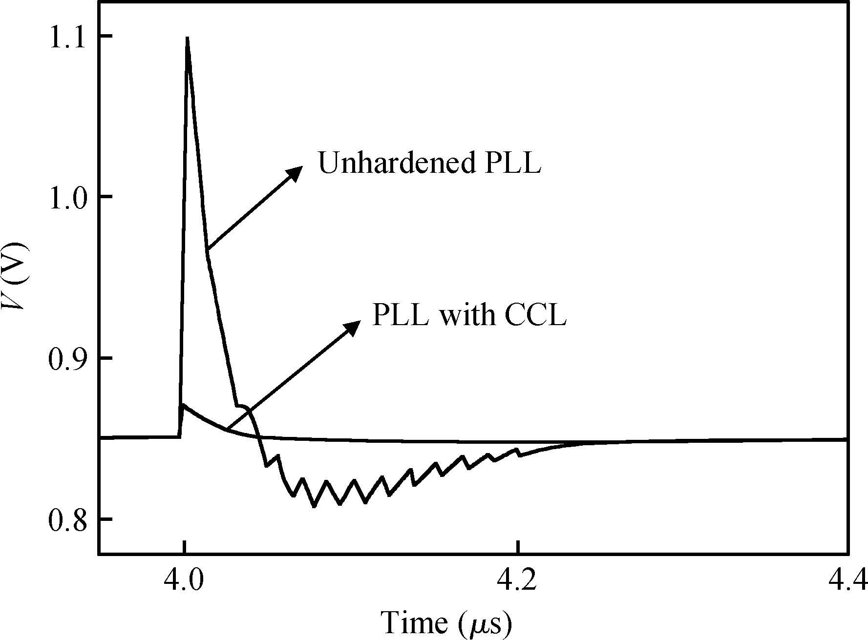
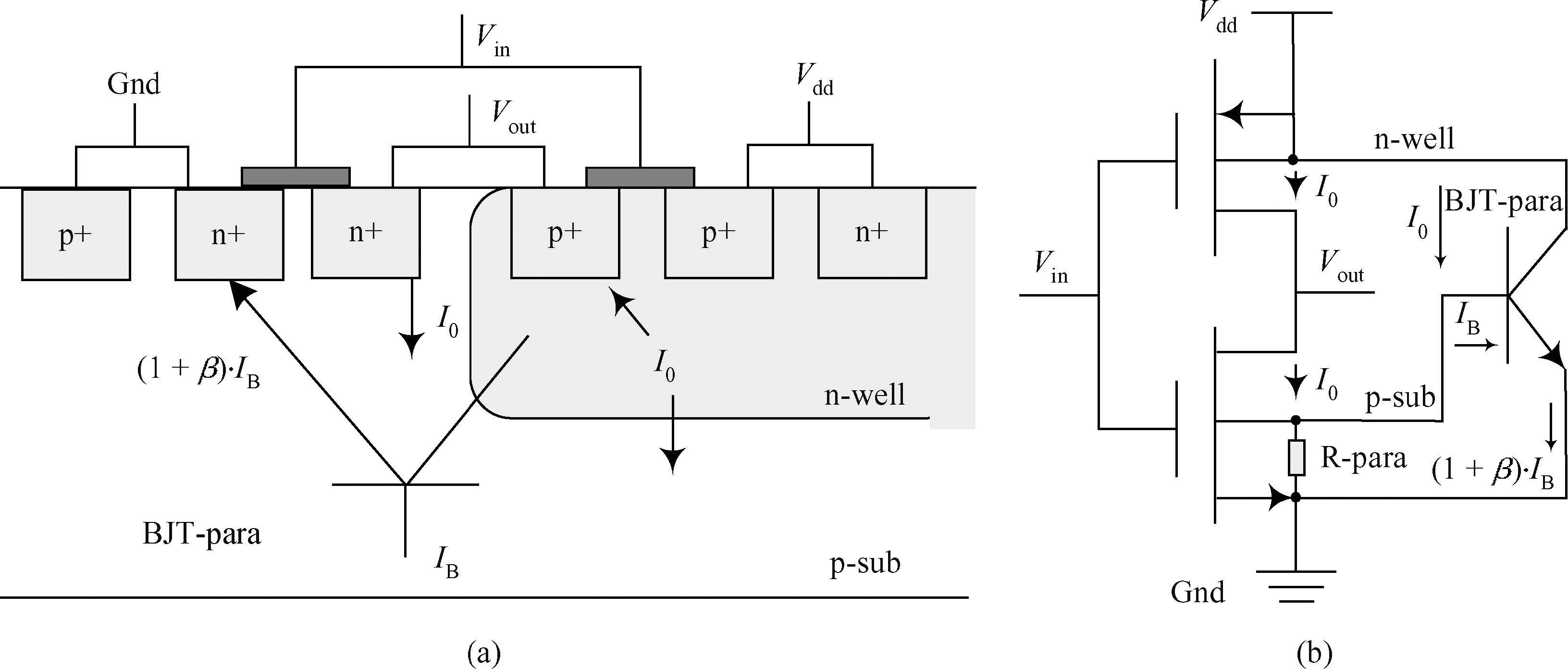
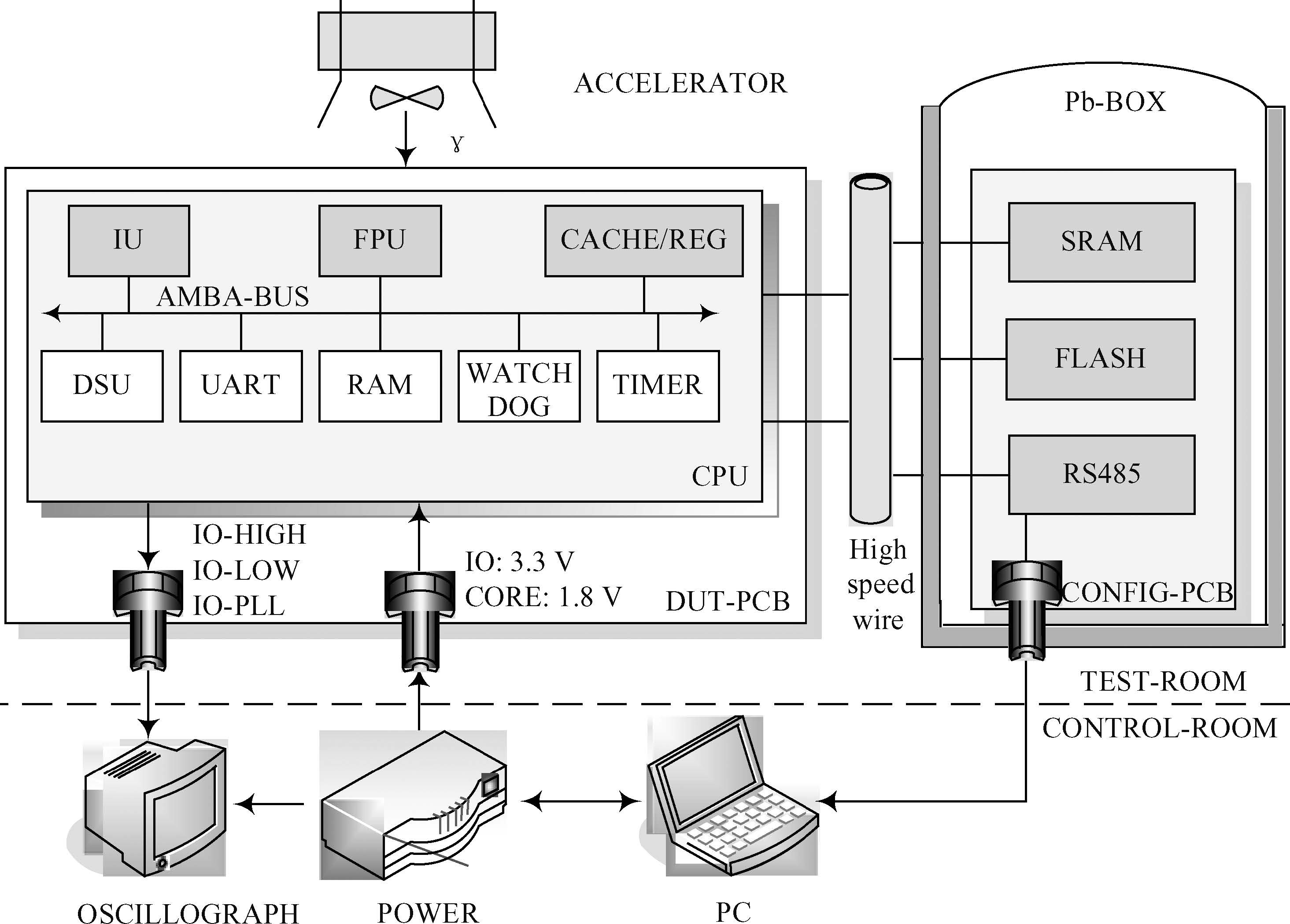
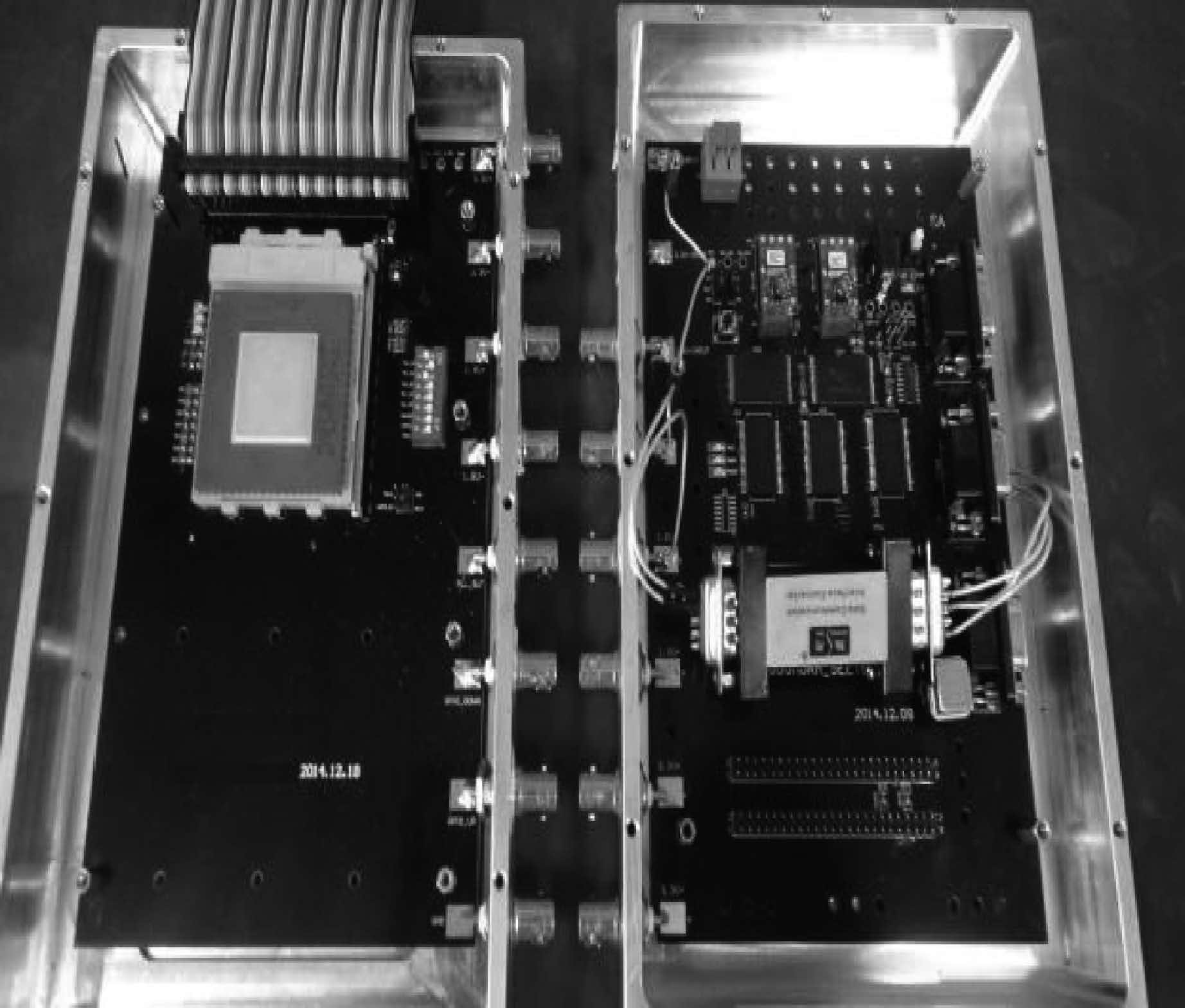
An experimental system is developed for the transient radiation effects testing of an anti-radiation hardened processor. Based on this system, the transient radiation effects in a microprocessor based on SPARC-V8 architecture was investigated. The dose-rate-soft-error index parameters of the processor were determined according to the test results, as were the influences on the function and timing parameters of the processor. The power supply balance is affected, which caused the system to reset and be the main source of soft errors. The results showed the circuit recovery time is primarily determined by the internal PLL, while the core power and the output-low-IO ports are more sensitive to the transient dose rate effect. The power-integrity-hardened design is proposed to mitigate the transient radiation effect.


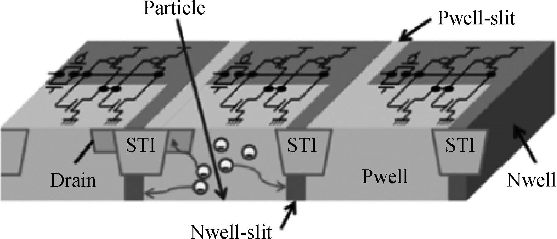
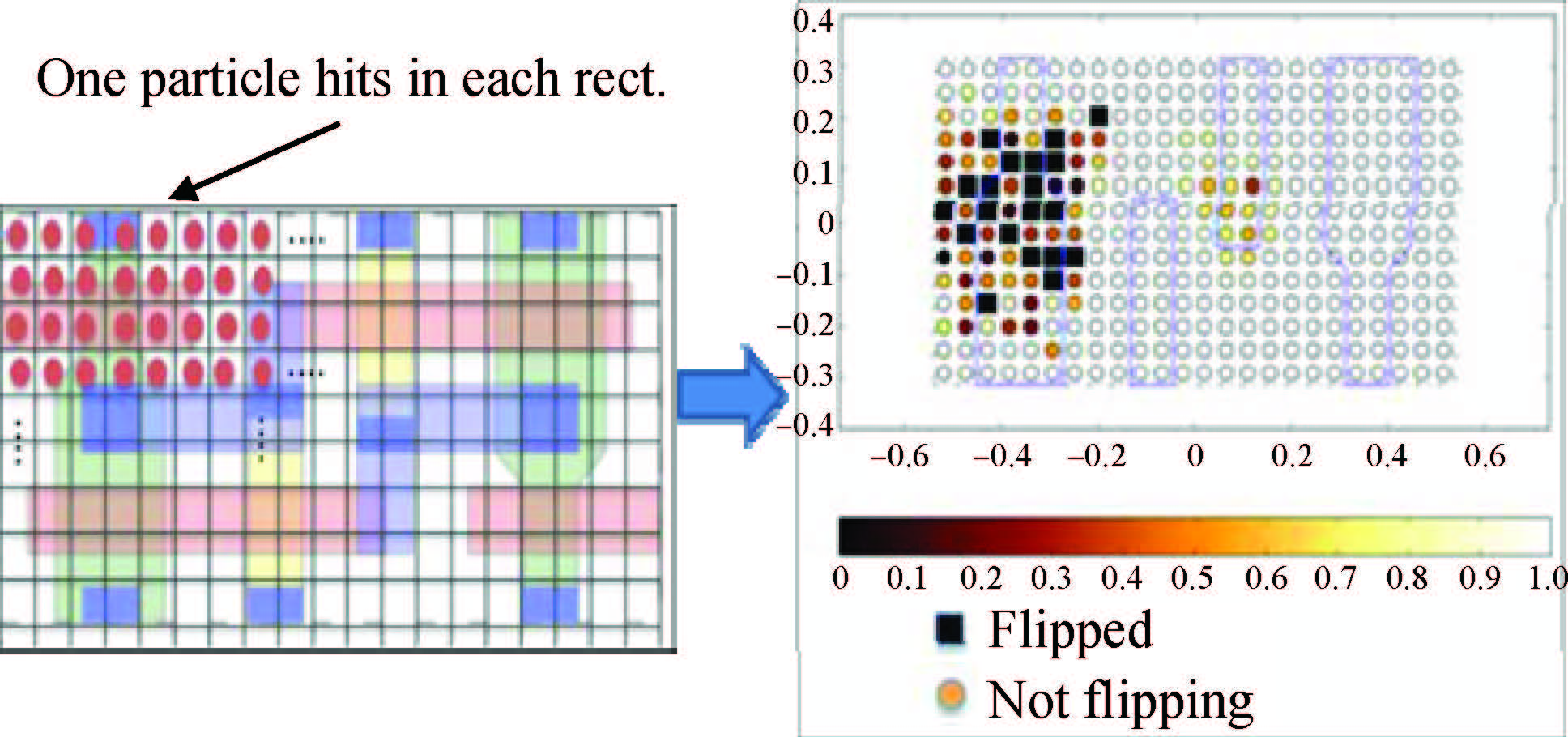
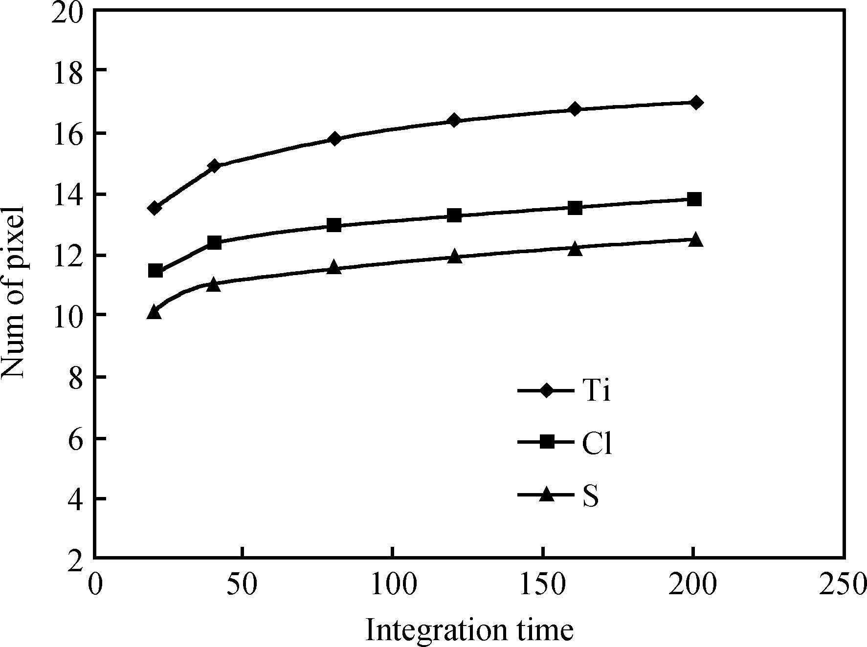
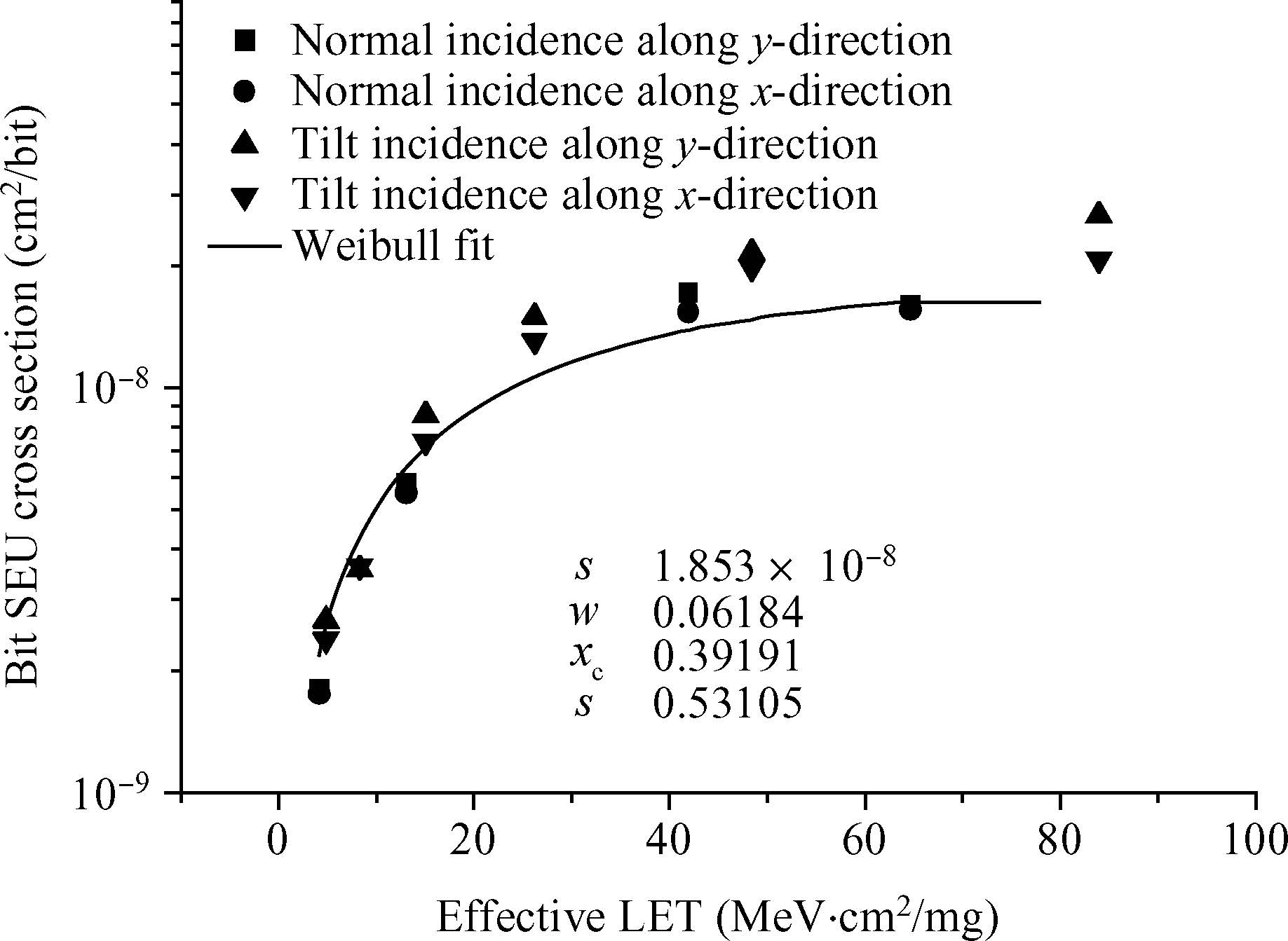
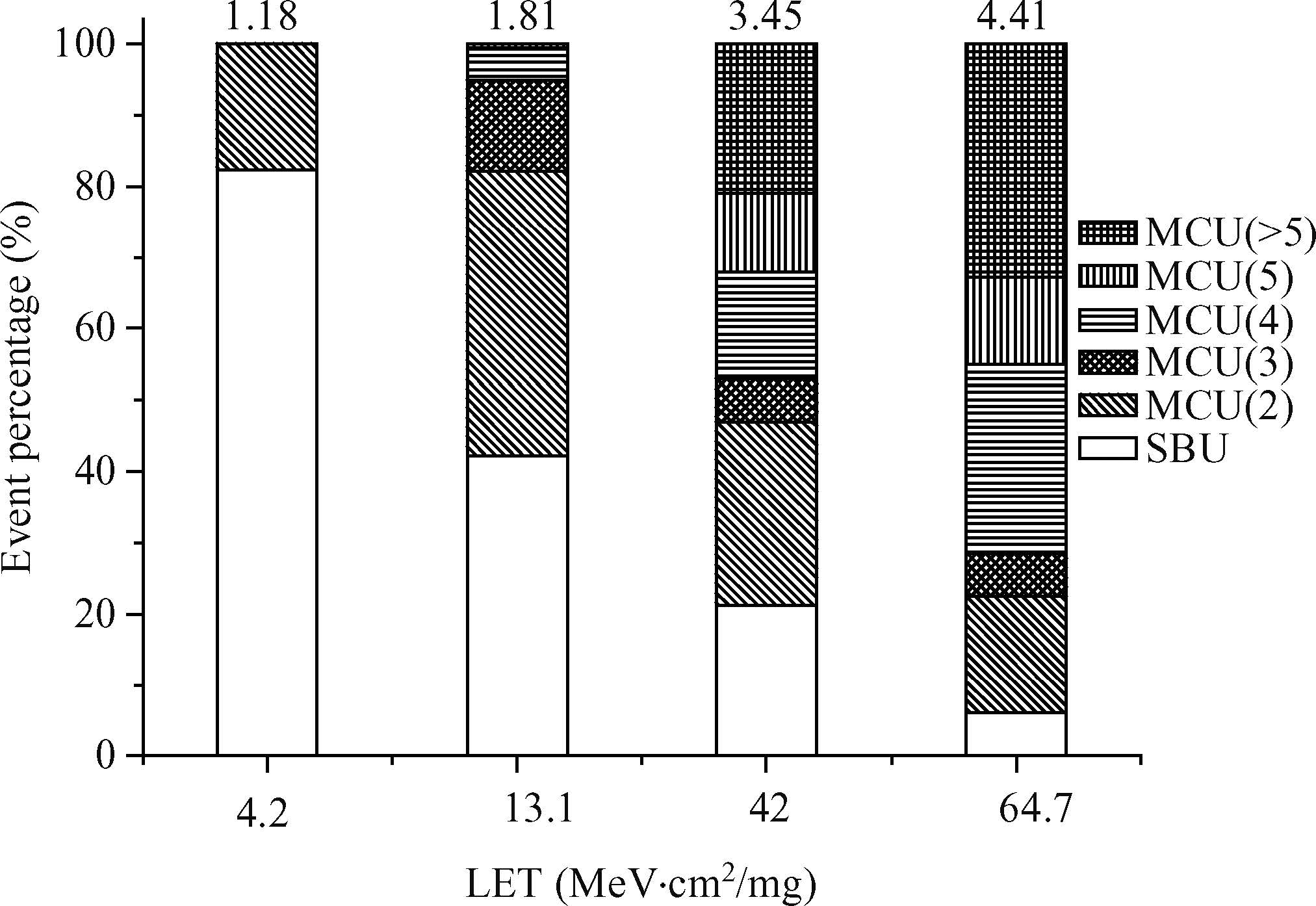
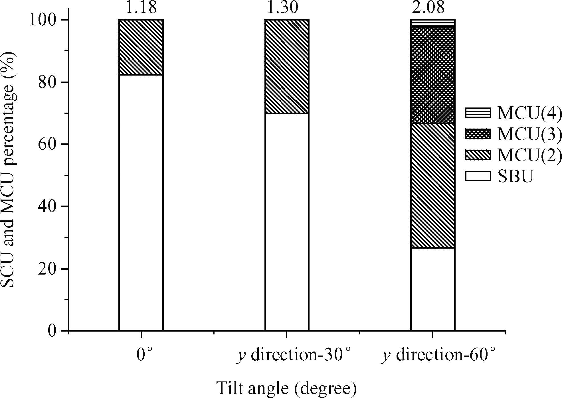
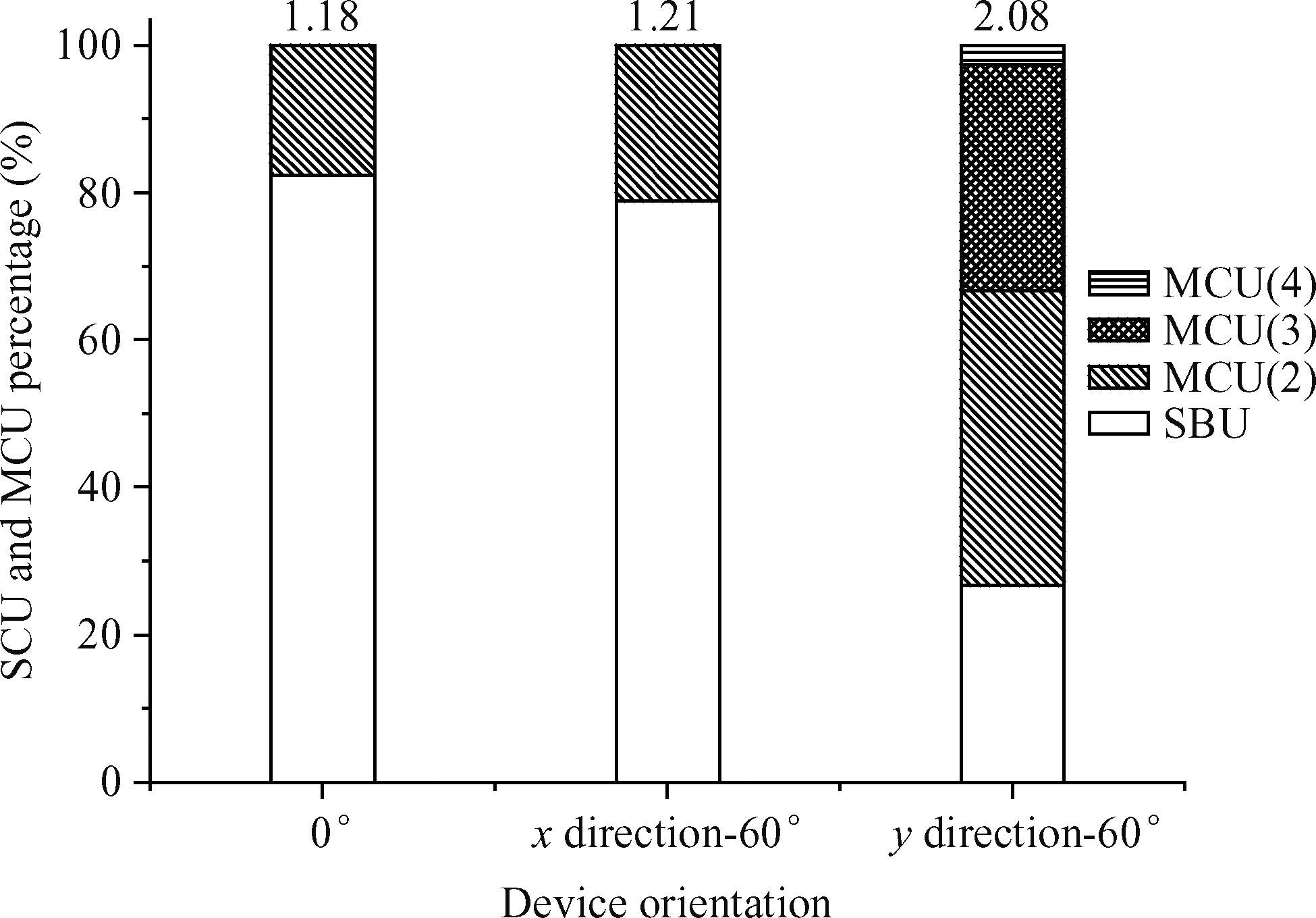
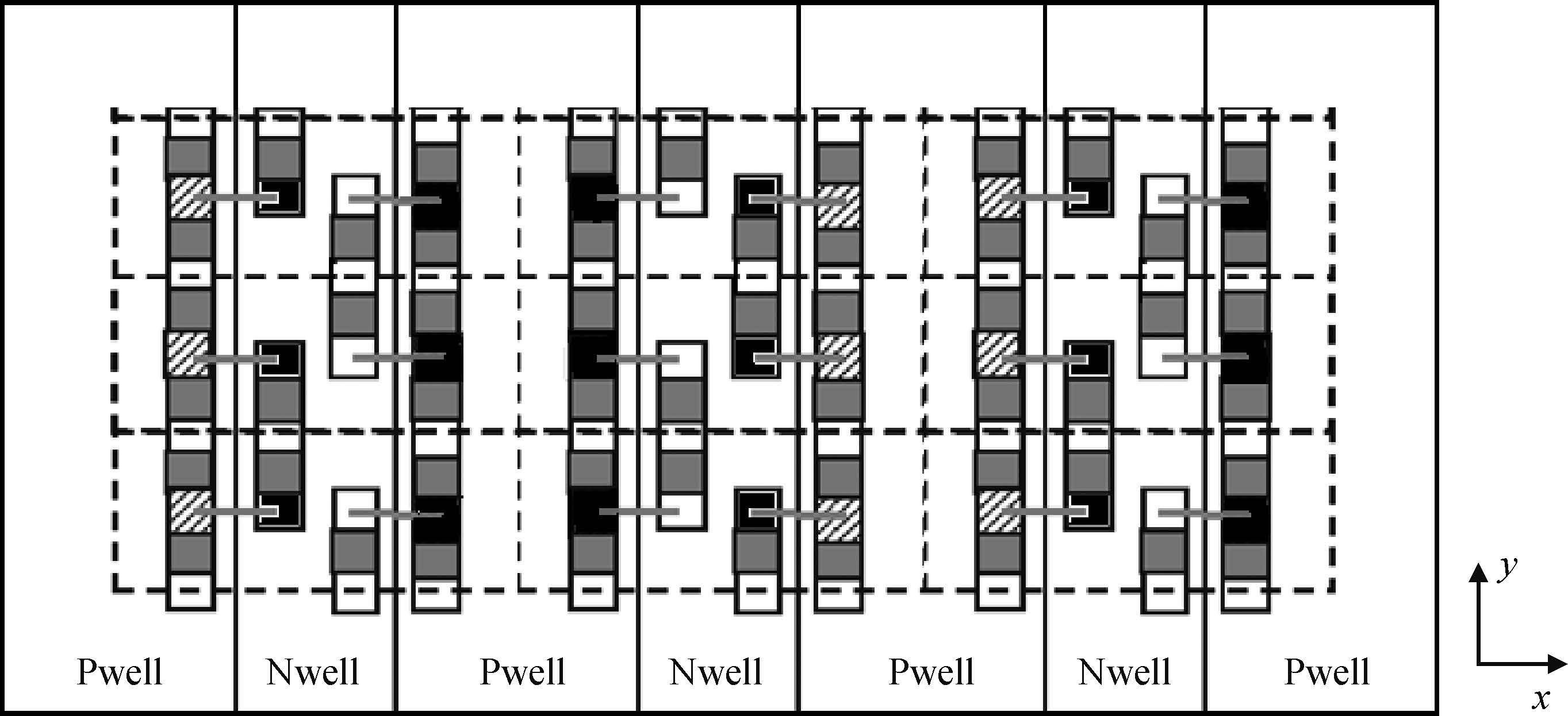
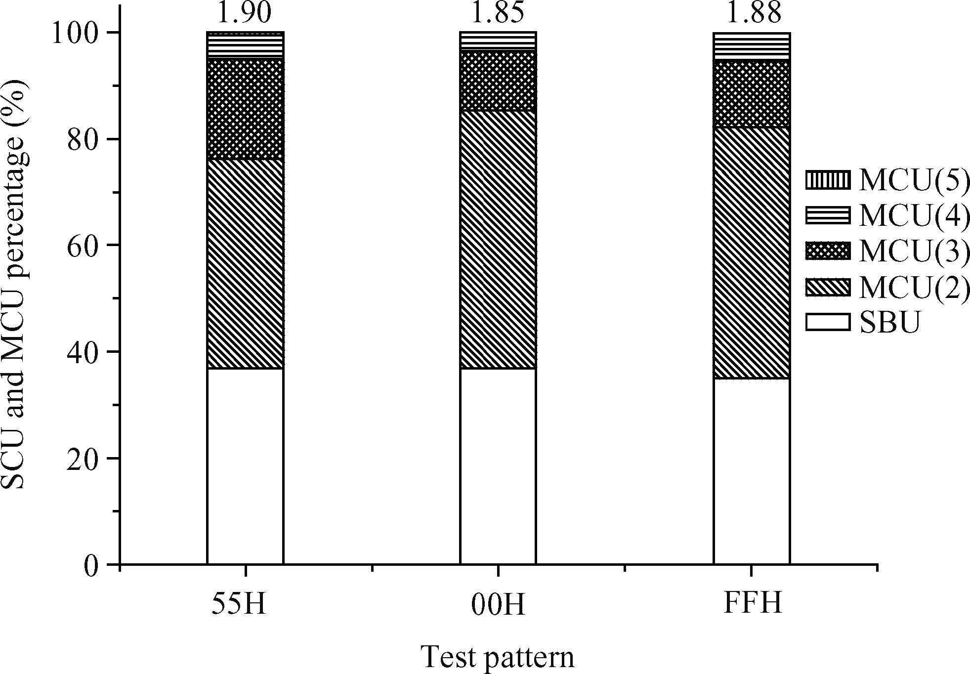
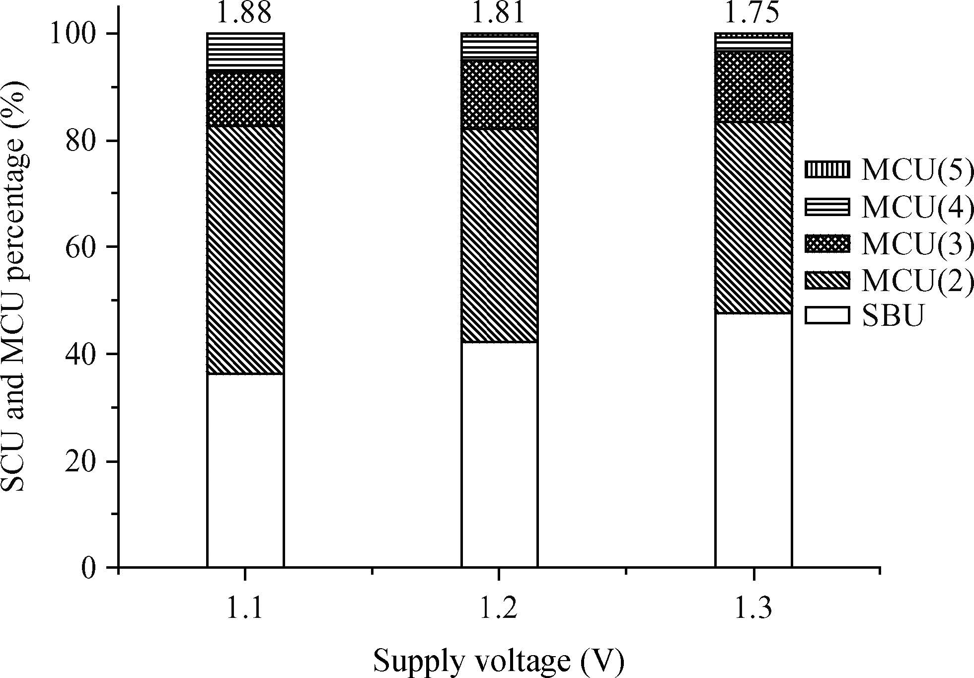
Single event multiple-cell upsets (MCU) increase sharply with the semiconductor devices scaling. The impacts of several test factors on heavy ion single event MCU in 65 nm SRAM are studied based on the buildup of MCU test data acquiring and processing technique, including the heavy ion LET, the tilt angle, the device orientation, the test pattern and the supply voltage; the MCU physical bitmaps are extracted correspondingly. The dependencies of parameters such as the MCU percentage, MCU mean and topological pattern on these factors are summarized and analyzed. This work is meaningful for developing a more reasonable single event test method and assessing the effectiveness of anti-MCU strategies on nanometer-scale devices.

We report on irradiation induced single event upset (SEU) by high-energy protons and heavy ions. The experiments were performed at the Paul Scherer Institute, and heavy ions at the SEE irradiating Facility on the HI-13 Tandem Accelerator in China's Institute of Atomic Energy, Beijing and the Heavy Ion Research Facility in Lanzhou in the Institute of Modern Physics, Chinese Academy of Sciences. The results of proton and heavy ions induced (SEU) in 65 nm bulk silicon CMOS SRAMS are discussed and the prediction on several typical orbits are presented.


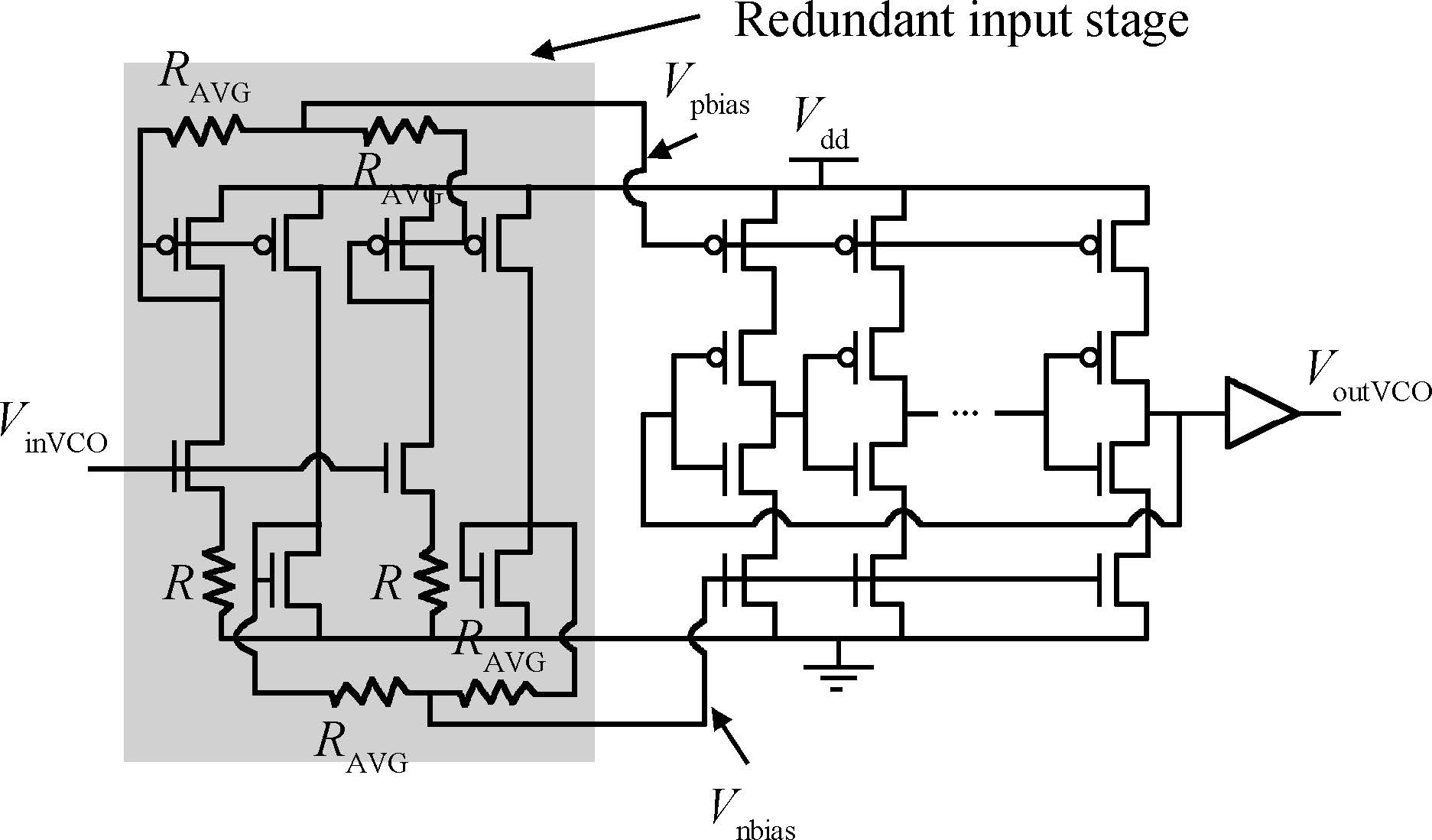
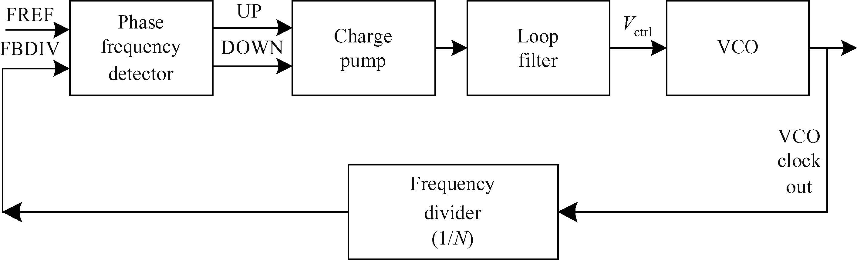
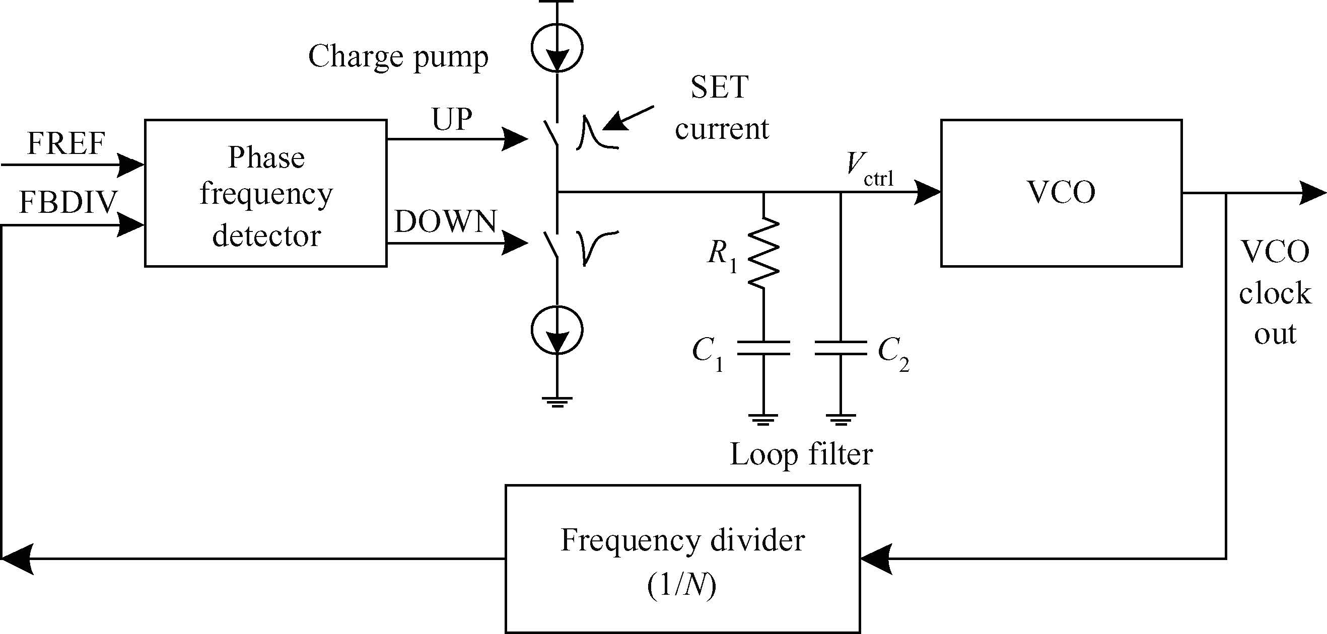
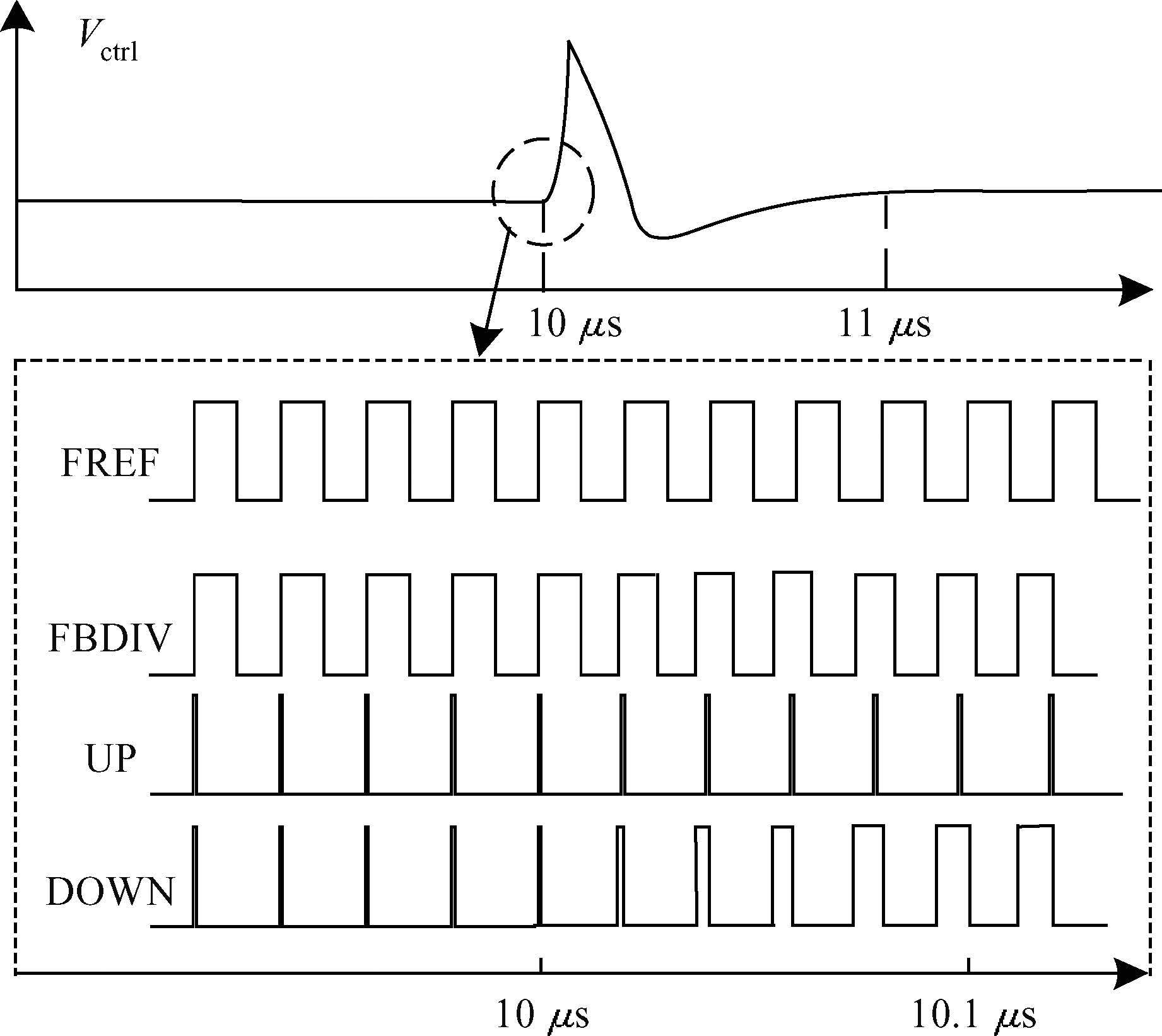
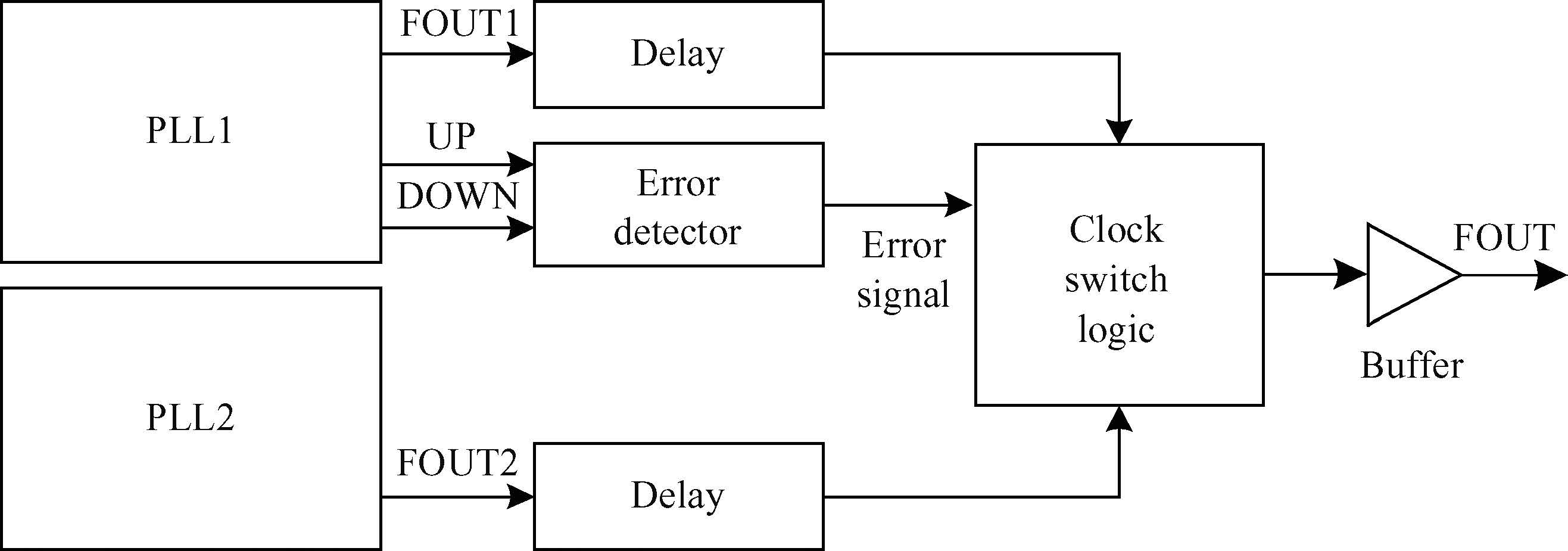
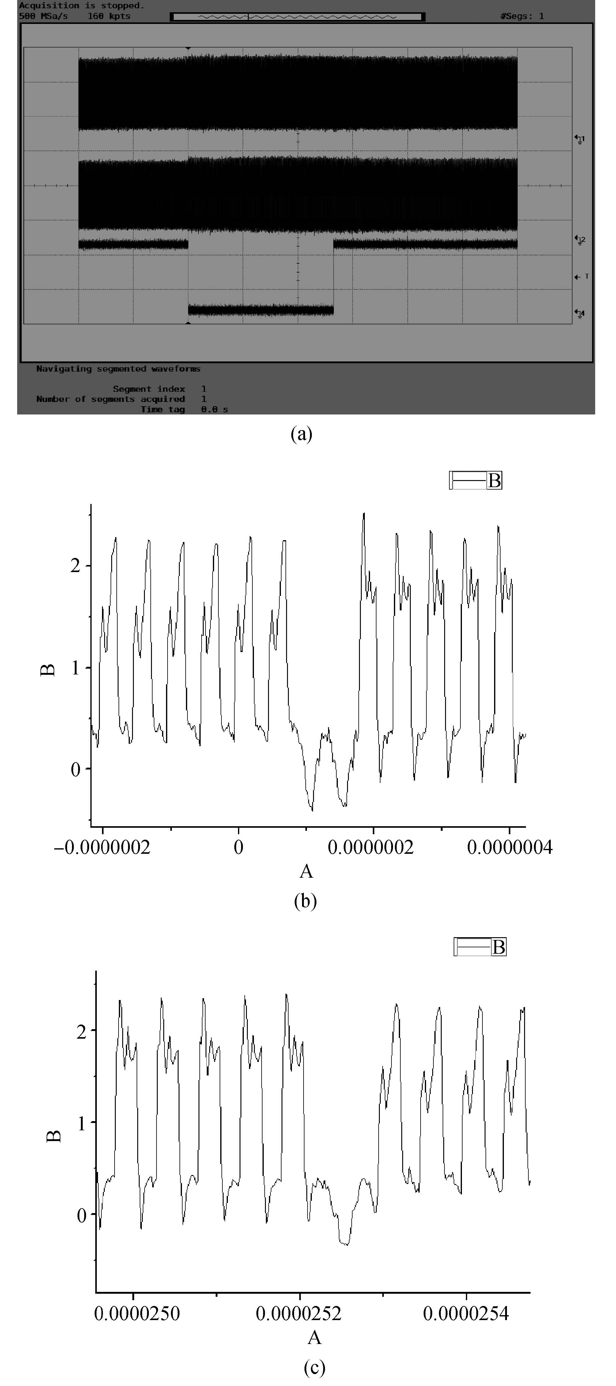
Single-event transient susceptibility of phase-locked loops has been investigated. The charge pump is the most sensitive component of the PLL to SET, and it is hard to mitigate this effect at the transistor level. A test circuit was designed on a 65 nm process using a new system-level radiation-hardening-by-design technique. Heavy-ion testing was used to evaluate the radiation hardness. Analyses and discussion of the feasibility of this method are also presented.


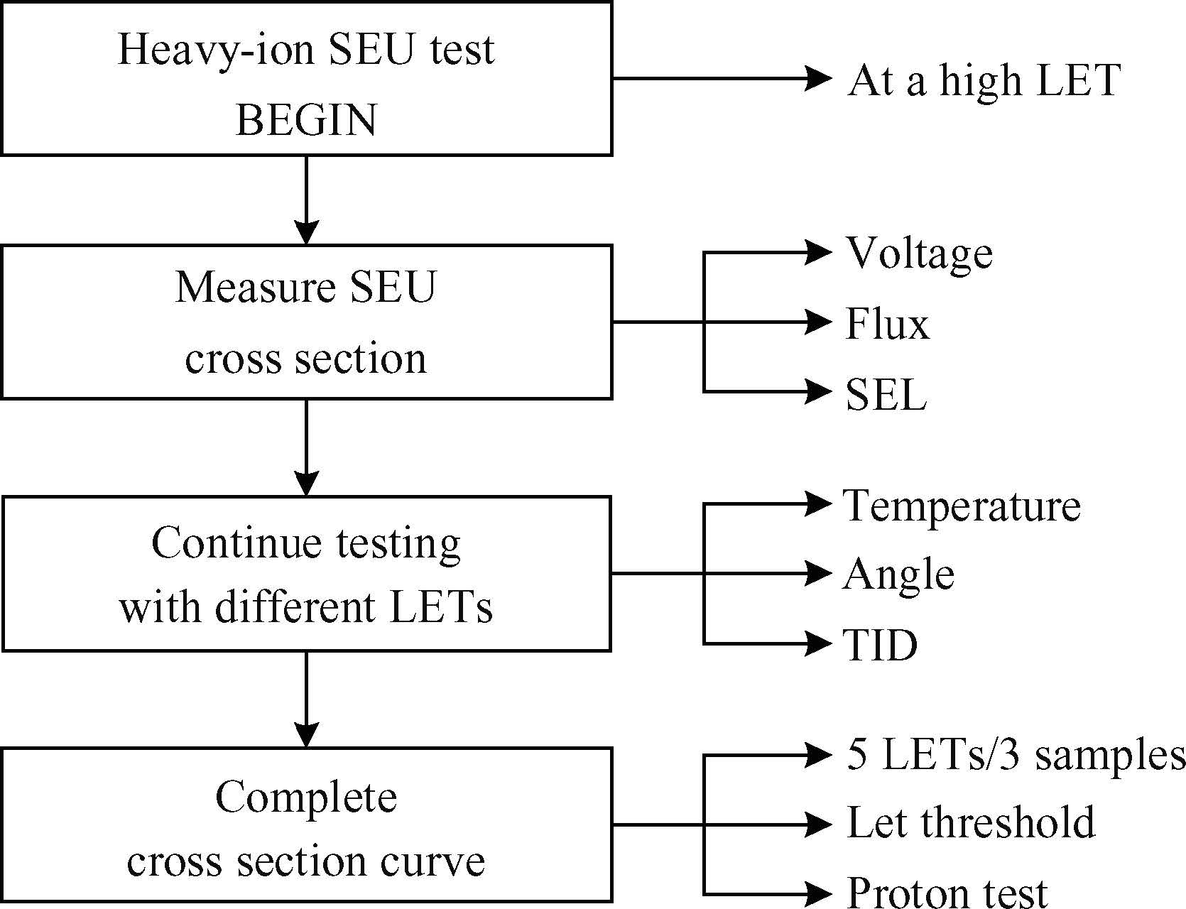
Single-event effects of nano scale integrated circuits are investigated. Evaluation methods for single-event transients, single-event upsets, and single-event functional interrupts in nano circuits are summarized and classified in detail. The difficulties in SEE testing are discussed as well as the development direction of test technology, with emphasis placed on the experimental evaluation of a nano circuit under heavy ion, proton, and laser irradiation. The conclusions in this paper are based on many years of testing at accelerator facilities and our present understanding of the mechanisms for SEEs, which have been well verified experimentally.
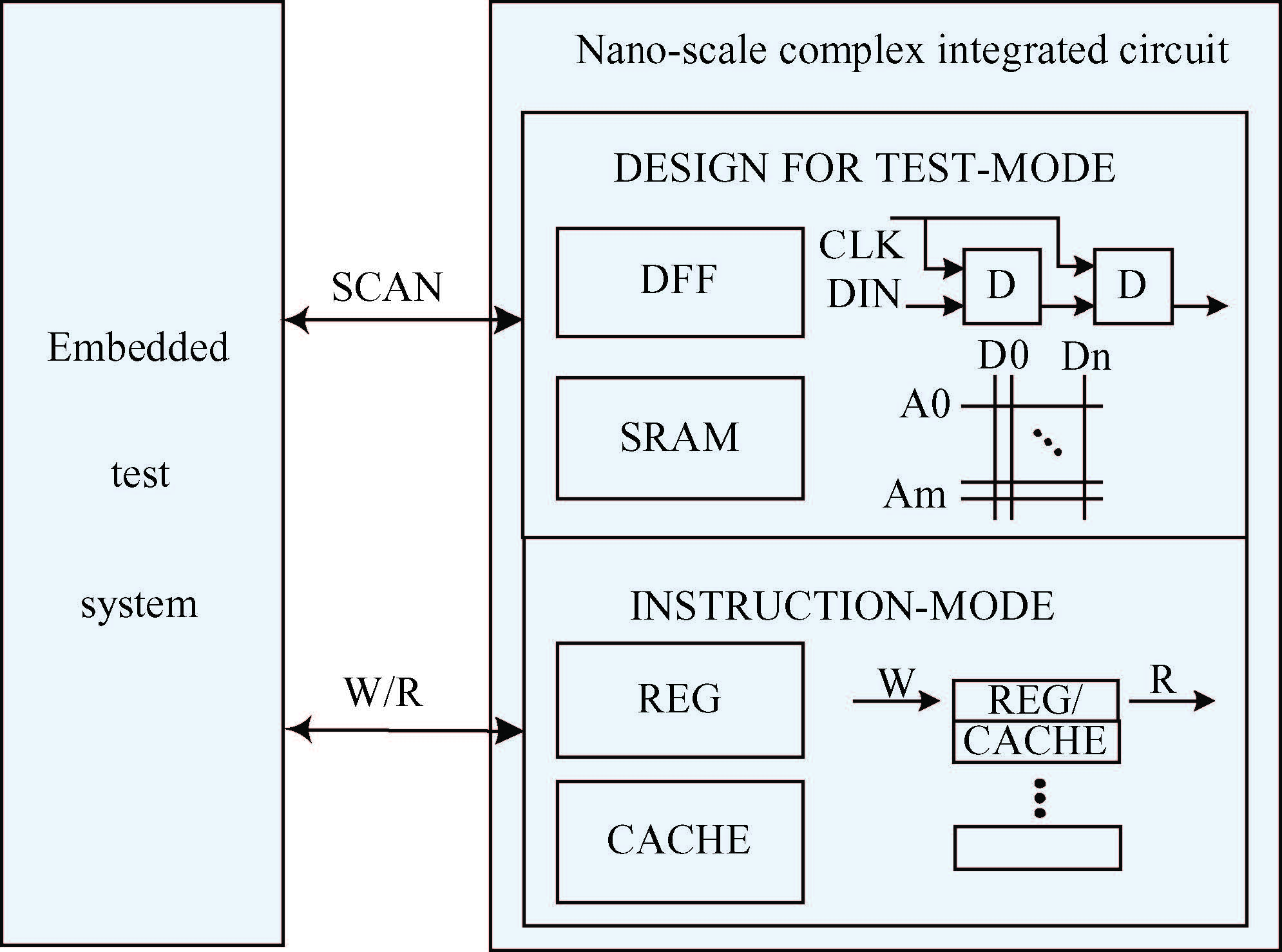
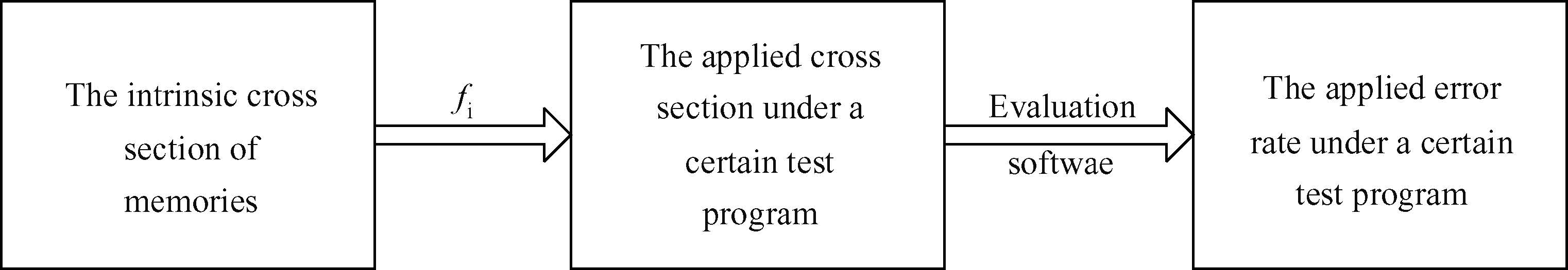


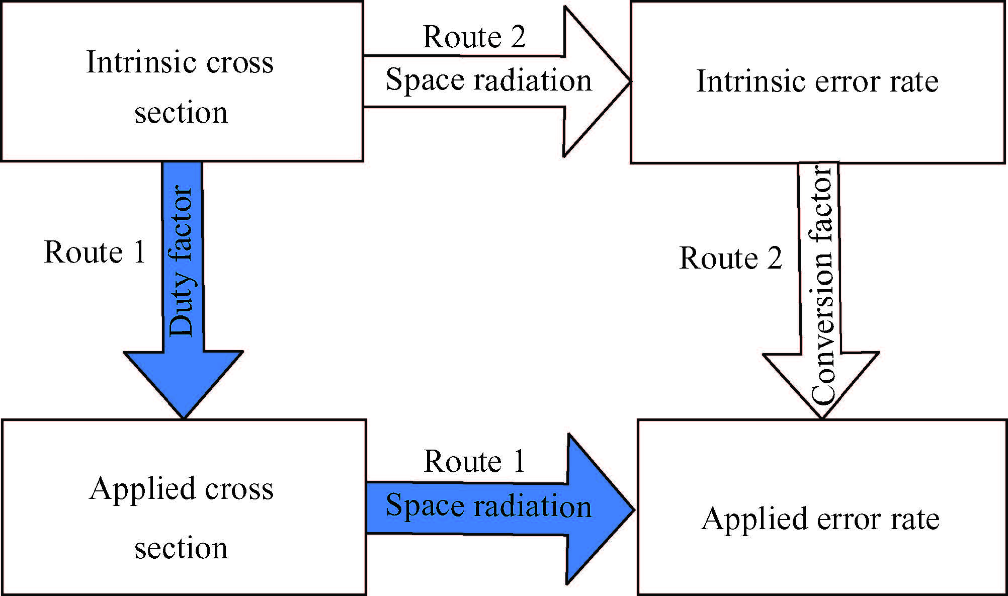
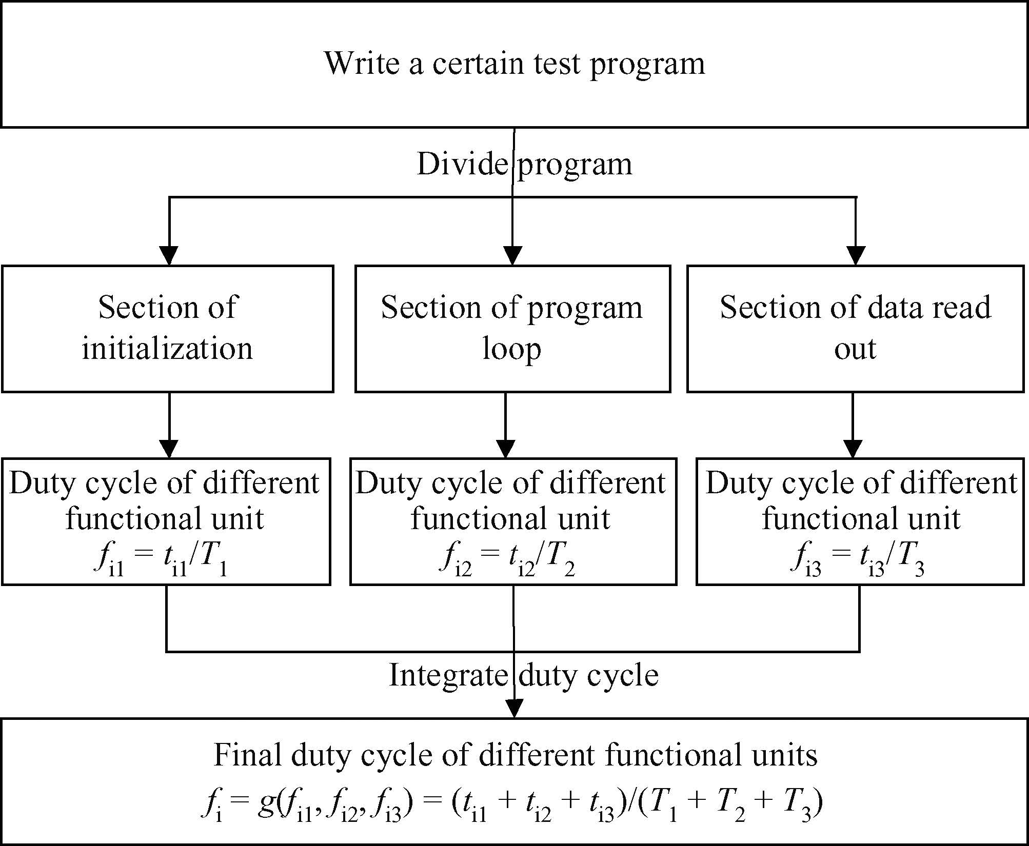
The sensitivity of complex integrated circuits to single-event effects is investigated. Sensitivity depends not only on the cross section of physical modules but also on the behavior of data patterns running on the system. A method dividing the main functional modules is proposed. The intrinsic cross section and the duty cycles of different sensitive modules are obtained during the execution of data patterns. A method for extracting the duty cycle is presented and a set of test patterns with different duty cycles are implemented experimentally. By combining the intrinsic cross section and the duty cycle of different sensitive modules, a universal method to predict SEE sensitivities of different test patterns is proposed, which is verified by experiments based on the target circuit of a microprocessor. Experimental results show that the deviation between prediction and experiment is less than 20%.


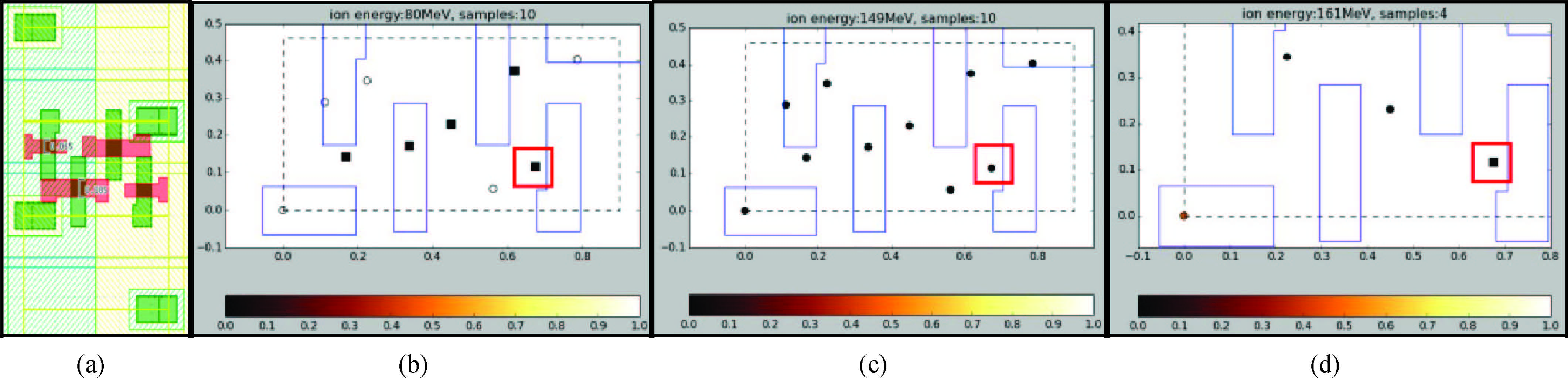
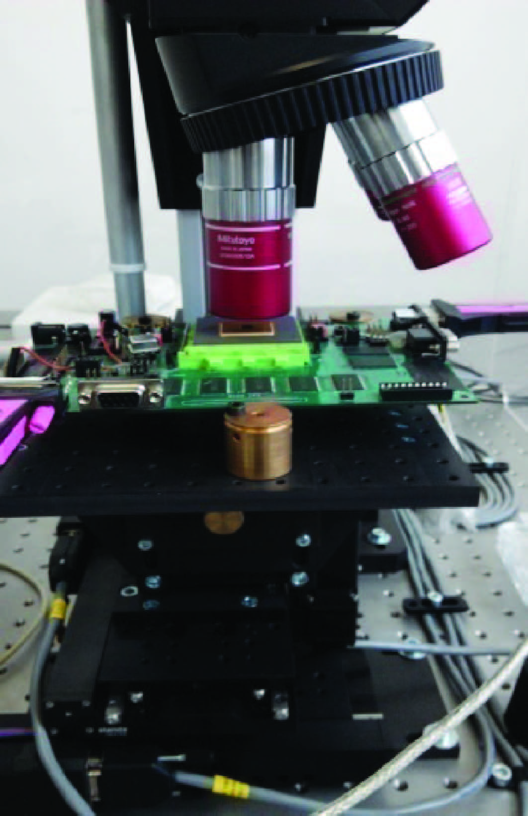
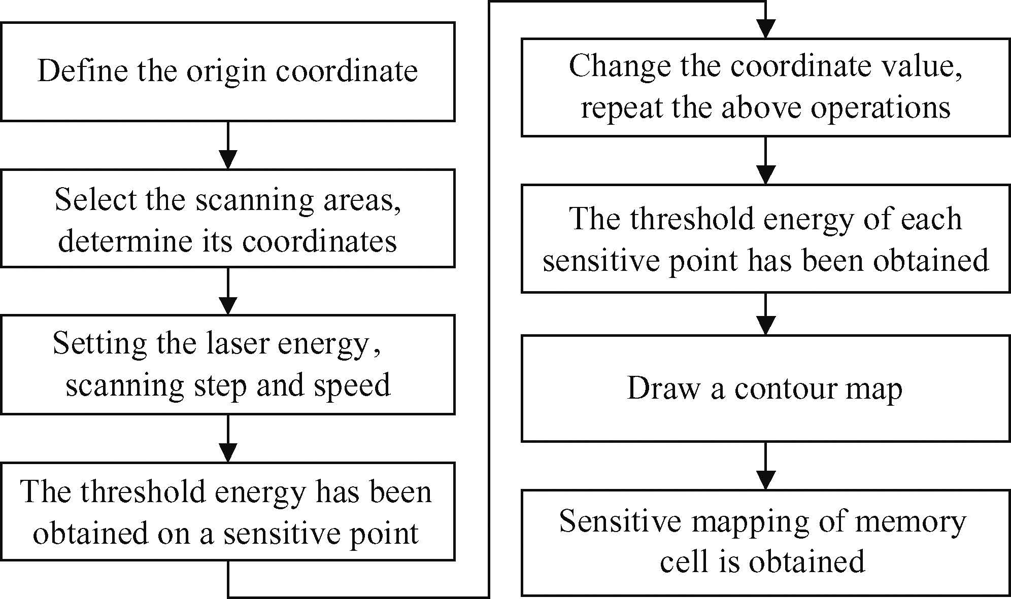
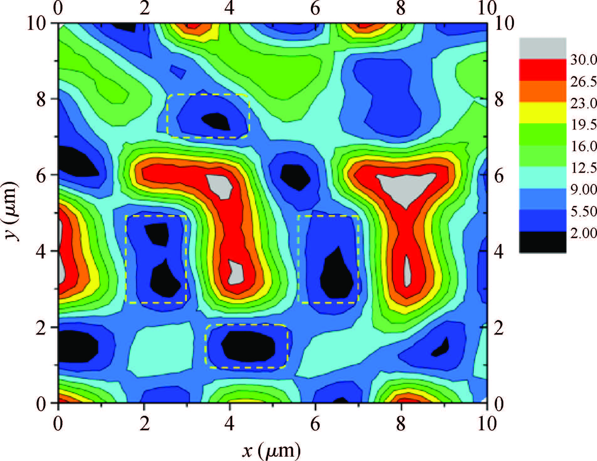
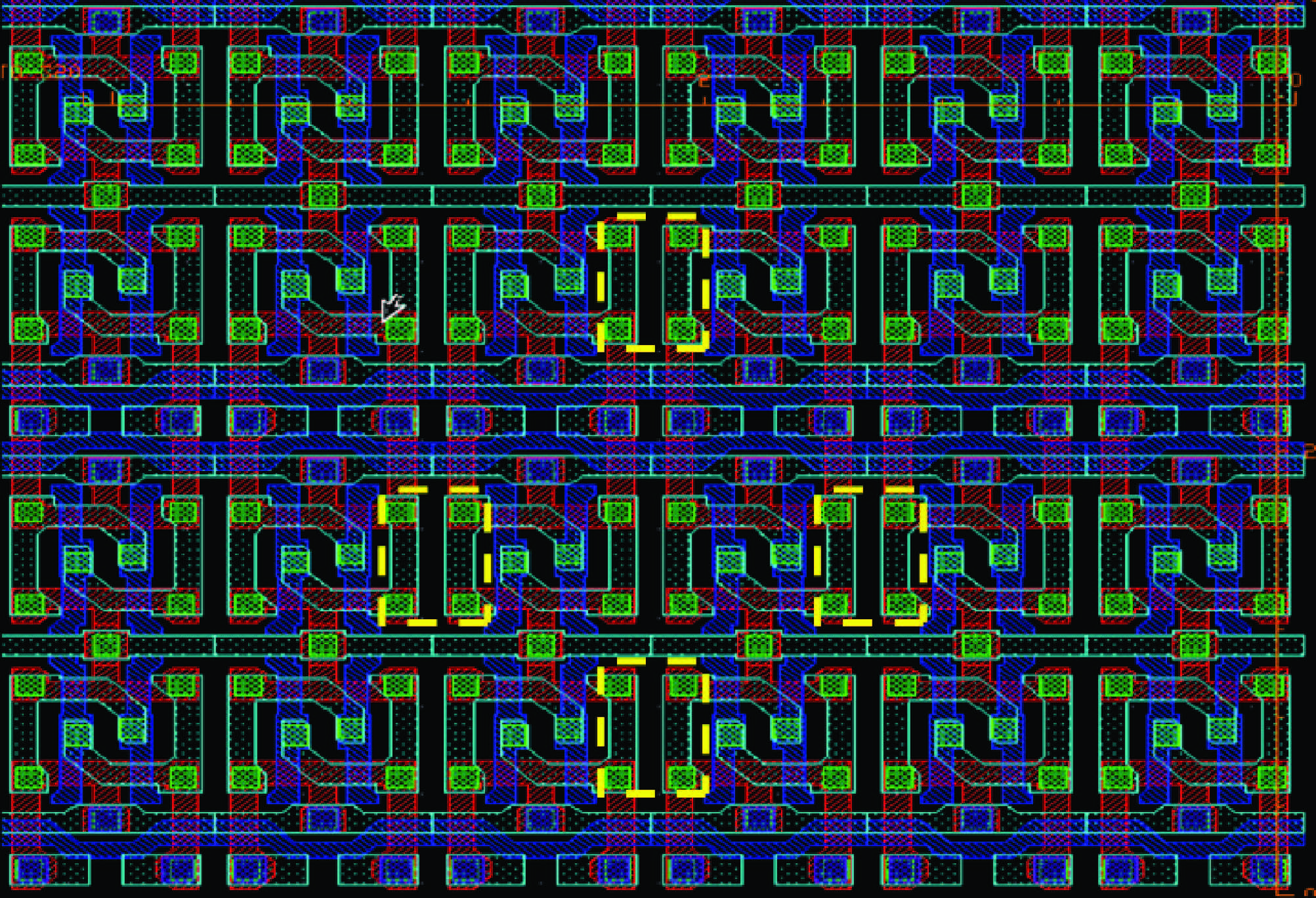
The single event effects of the sensitivity of a circuit are investigated on a 32-bit microprocessor with a five-stage instruction pipeline by pulsed laser test. The investigation on sensitive mapping of the memory cell is illustrated and then the comparison between the sensitive mapping and the layout of the circuit is made. A comparison result indicates that the area of the sensitive node in sensitive mapping is just the location of the drain in the layout. Therefore, SEE sensitivity in sensitive mapping fits well with that in the physical layout of functional units, which can directly and objectively indicate the size and distribution of sensitive areas. The investigation of sensitive mapping is a meaningful way to verify the hardened effect and provide a reference for improving hardened design by combining with the physical layout.


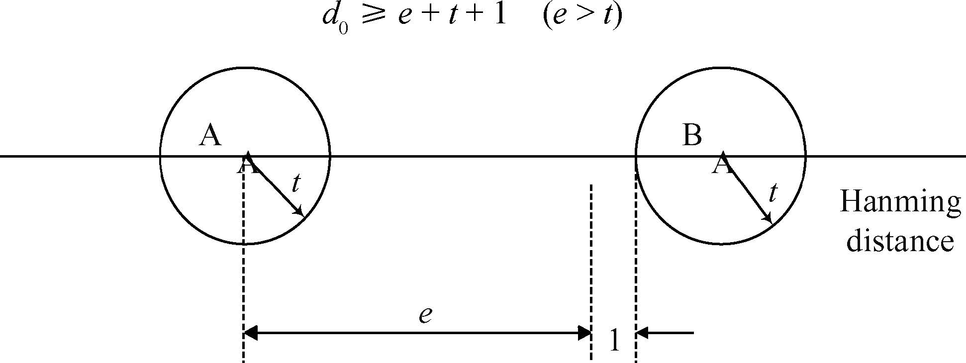
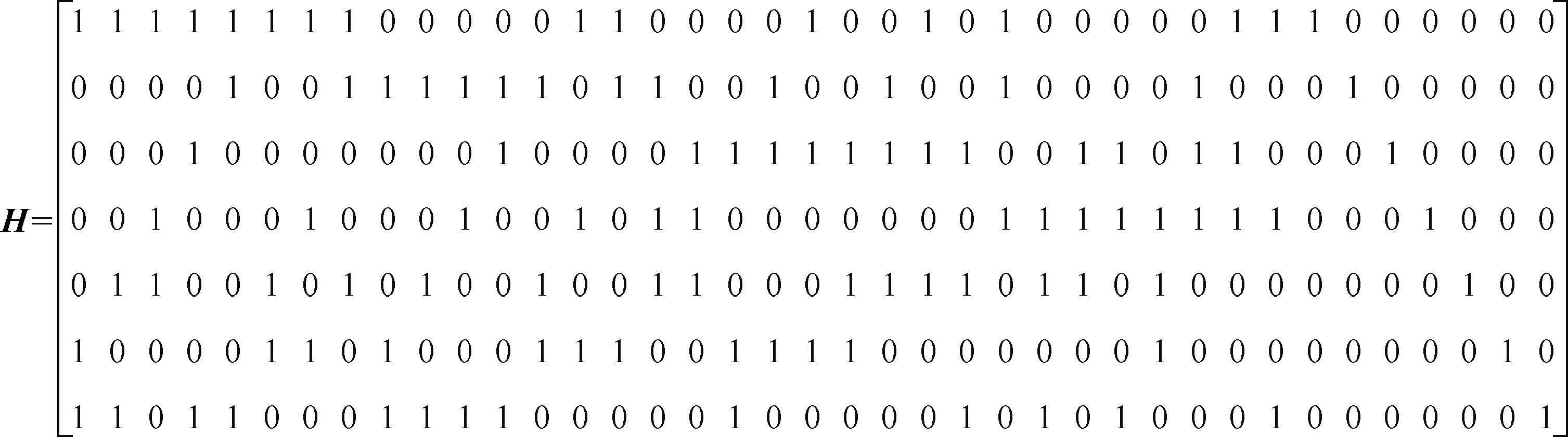
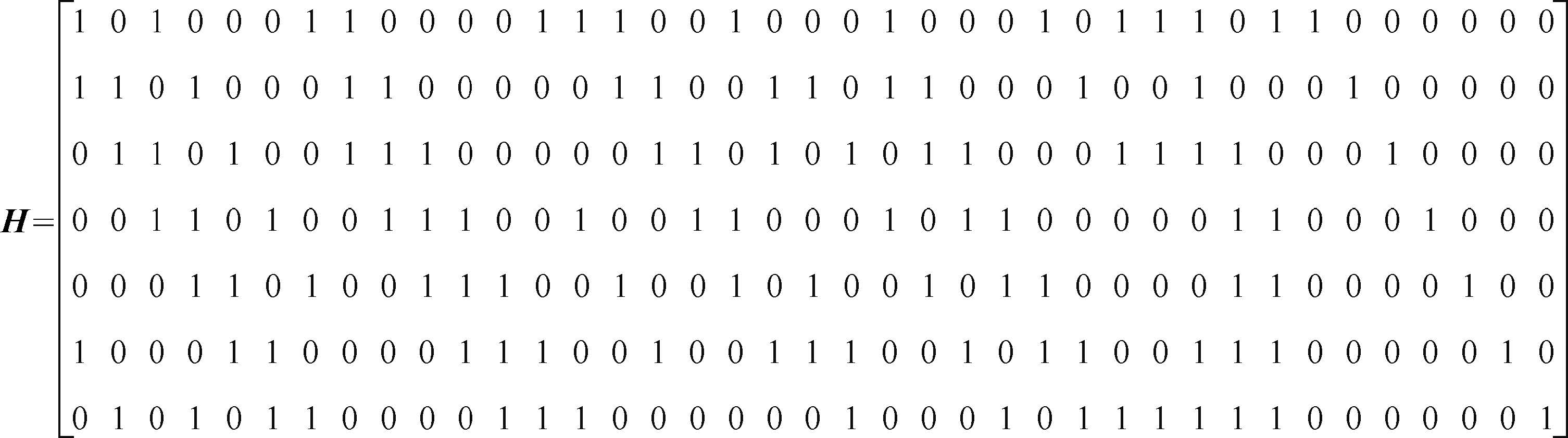
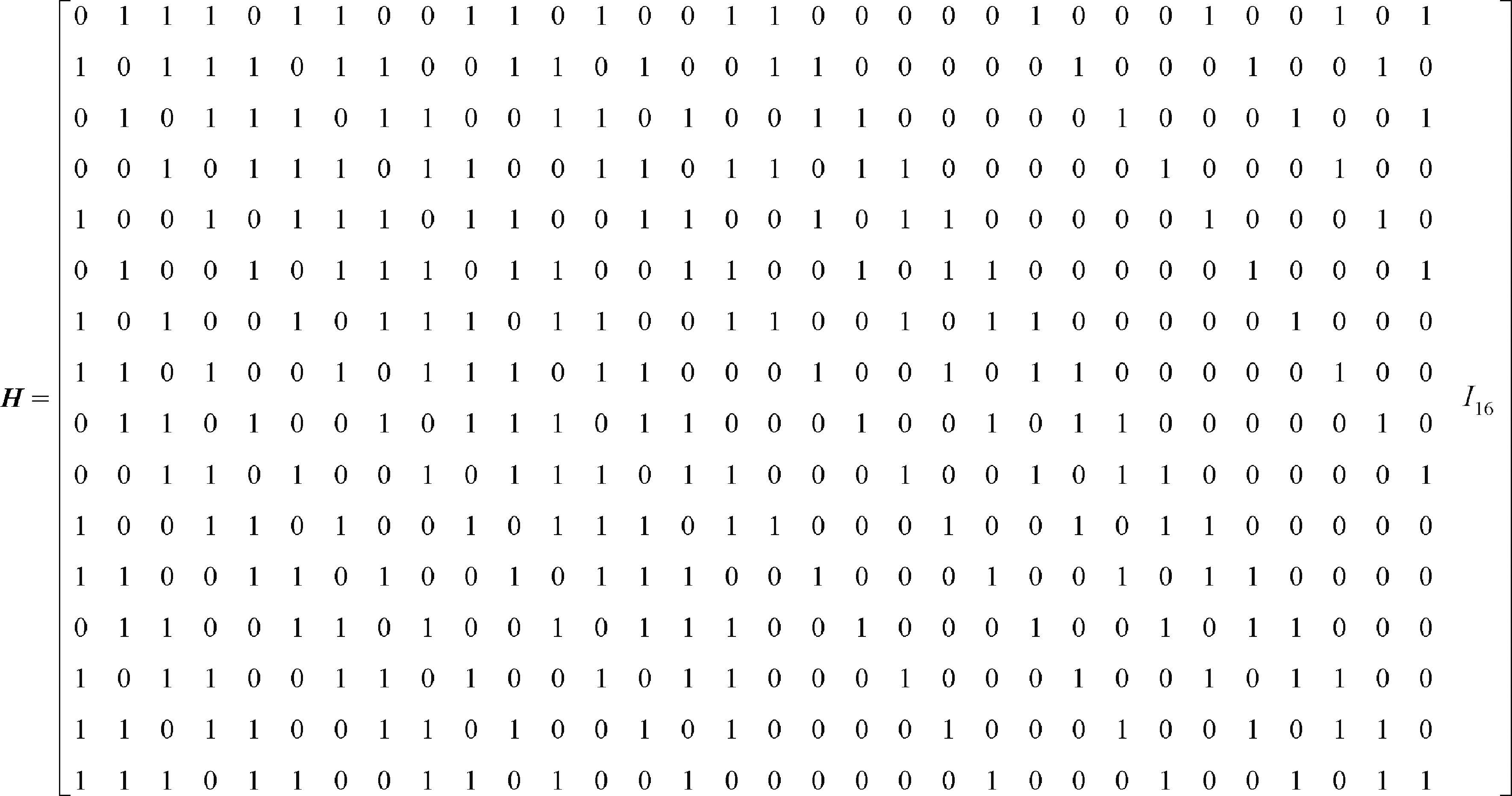
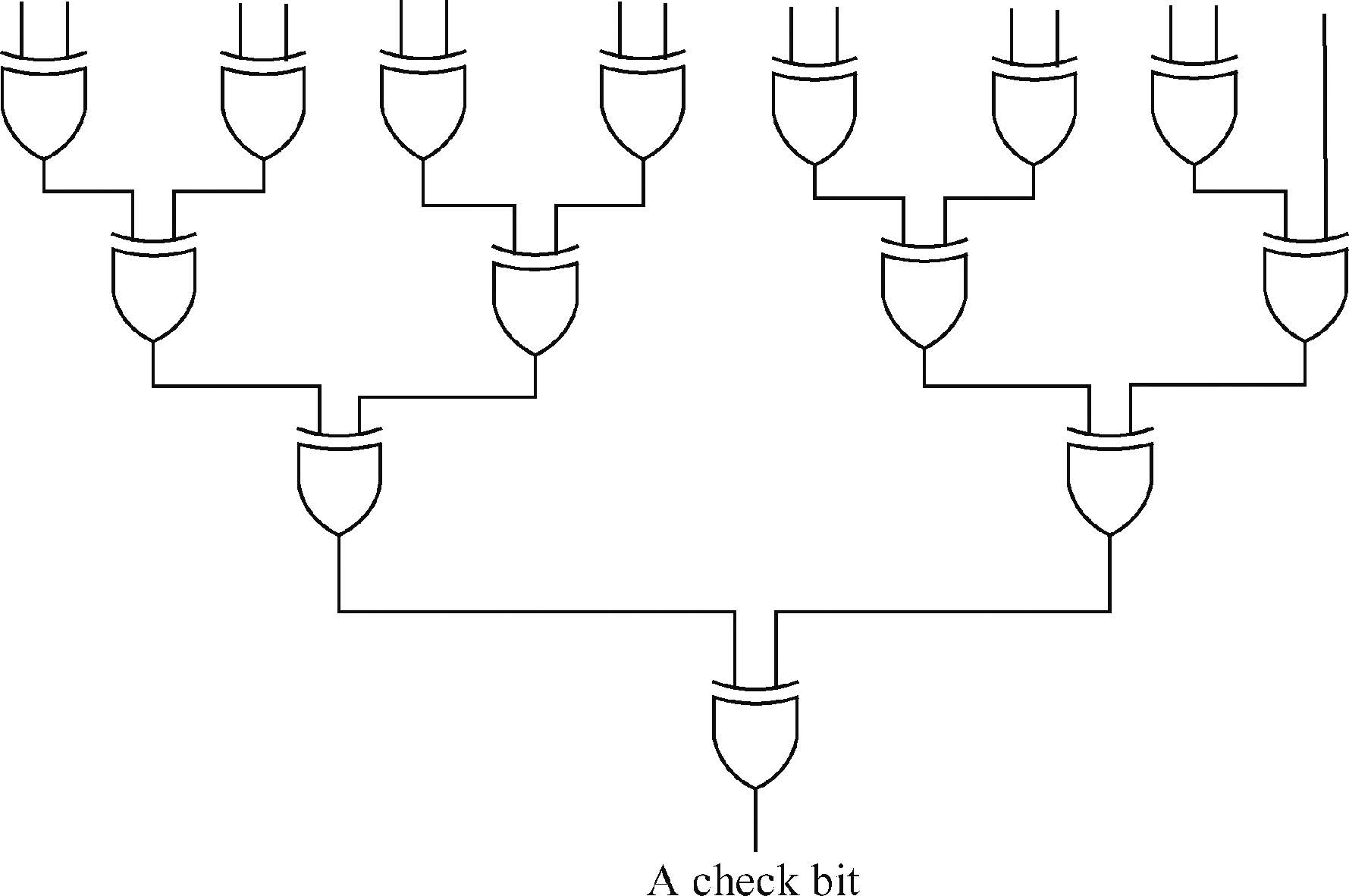
An optimization method of error detection and correction (EDAC) circuit design is proposed. The method involves selecting or constructing EDAC codes of low cost hardware, associated with operation scheduling implementation based on 2-input XOR gates structure, and two actions for reducing hardware cells, which can reduce the delay penalties and area costs of the EDAC circuit effectively. The 32-bit EDAC circuit hardware implementation is selected to make a prototype, based on the 180 nm process. The delay penalties and area costs of the EDAC circuit are evaluated. Results show that the time penalty and area cost of the EDAC circuitries are affected with different parity-check matrices and different hardware implementation for the EDAC codes with the same capability of correction and detection code. This method can be used as a guide for low-cost radiation-hardened microprocessor EDAC circuit design and for more advanced technologies.

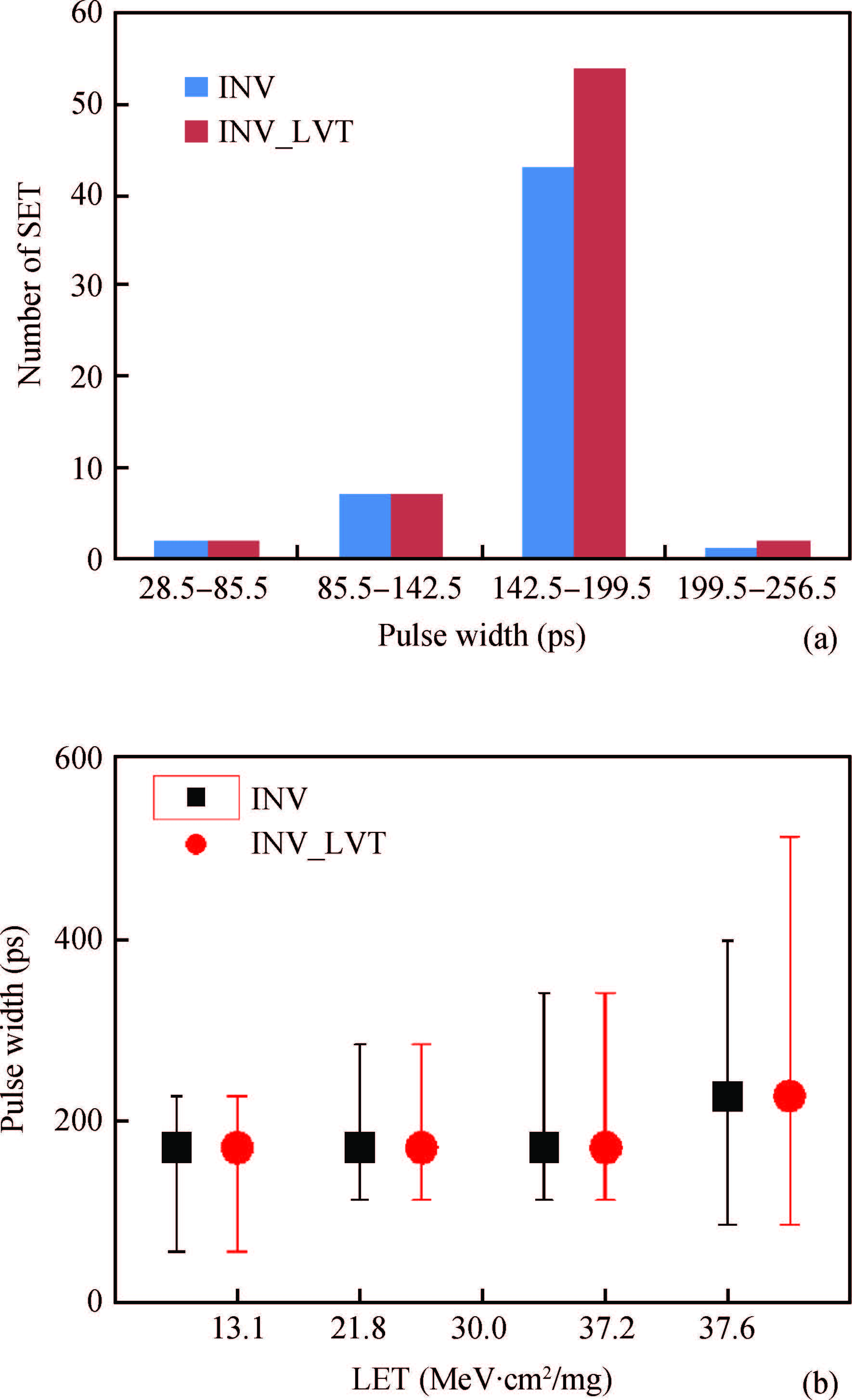
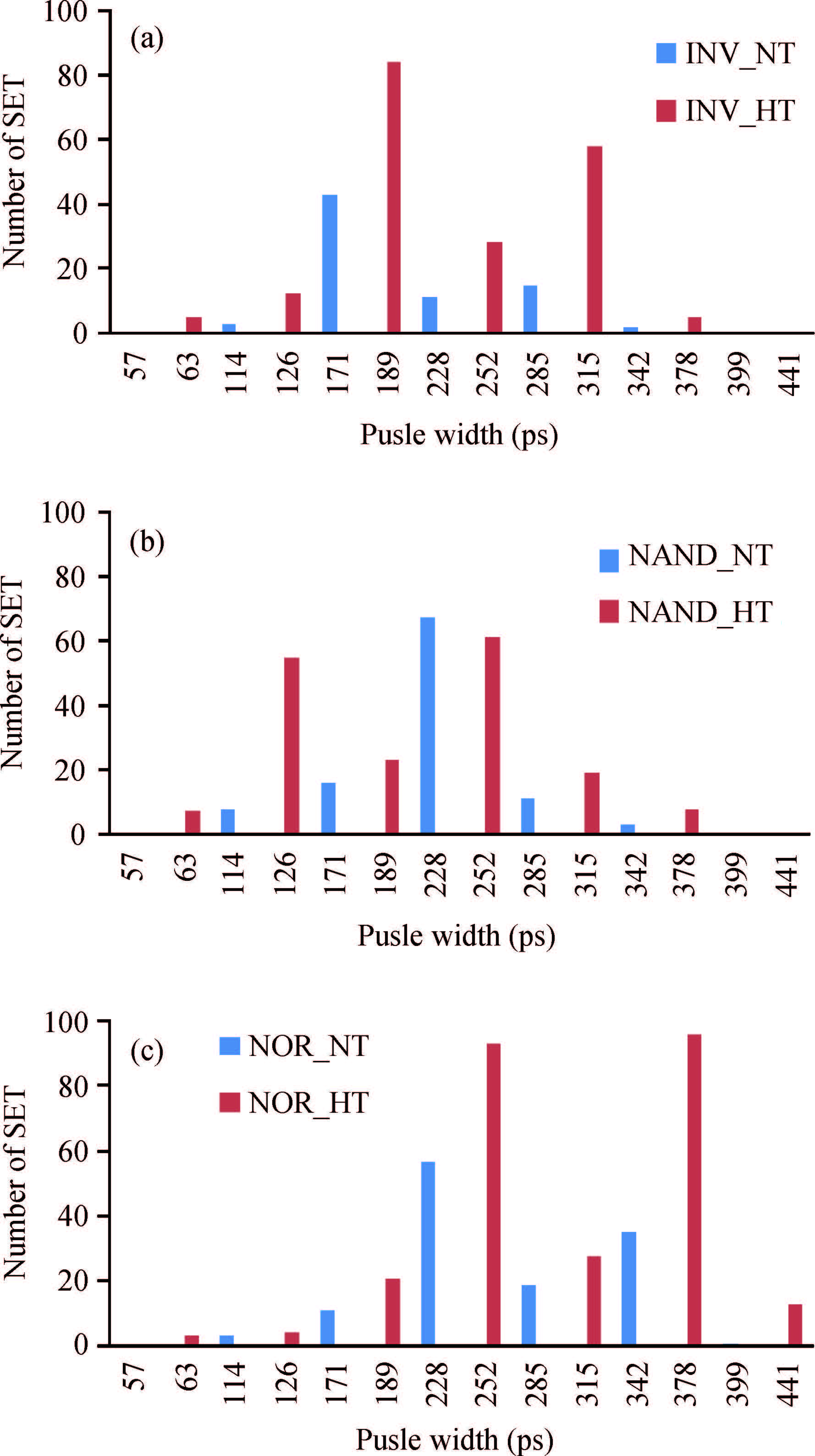
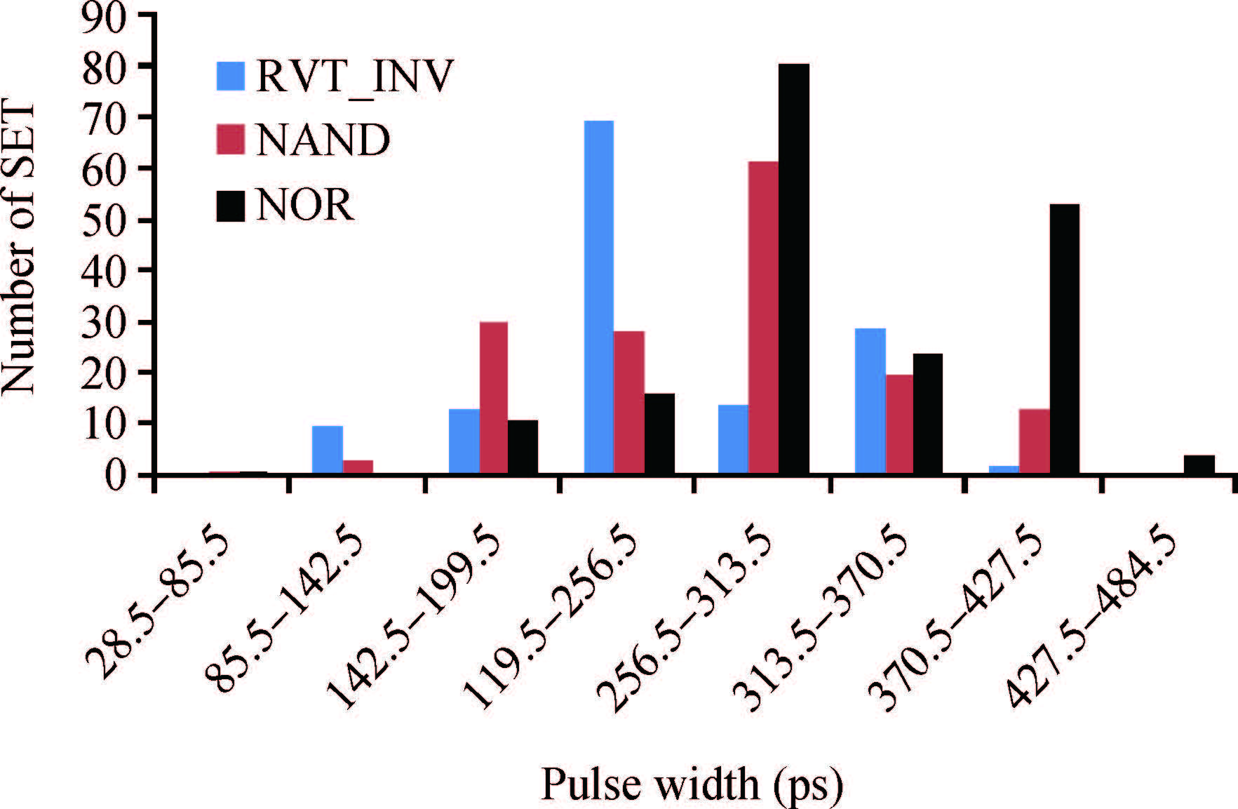
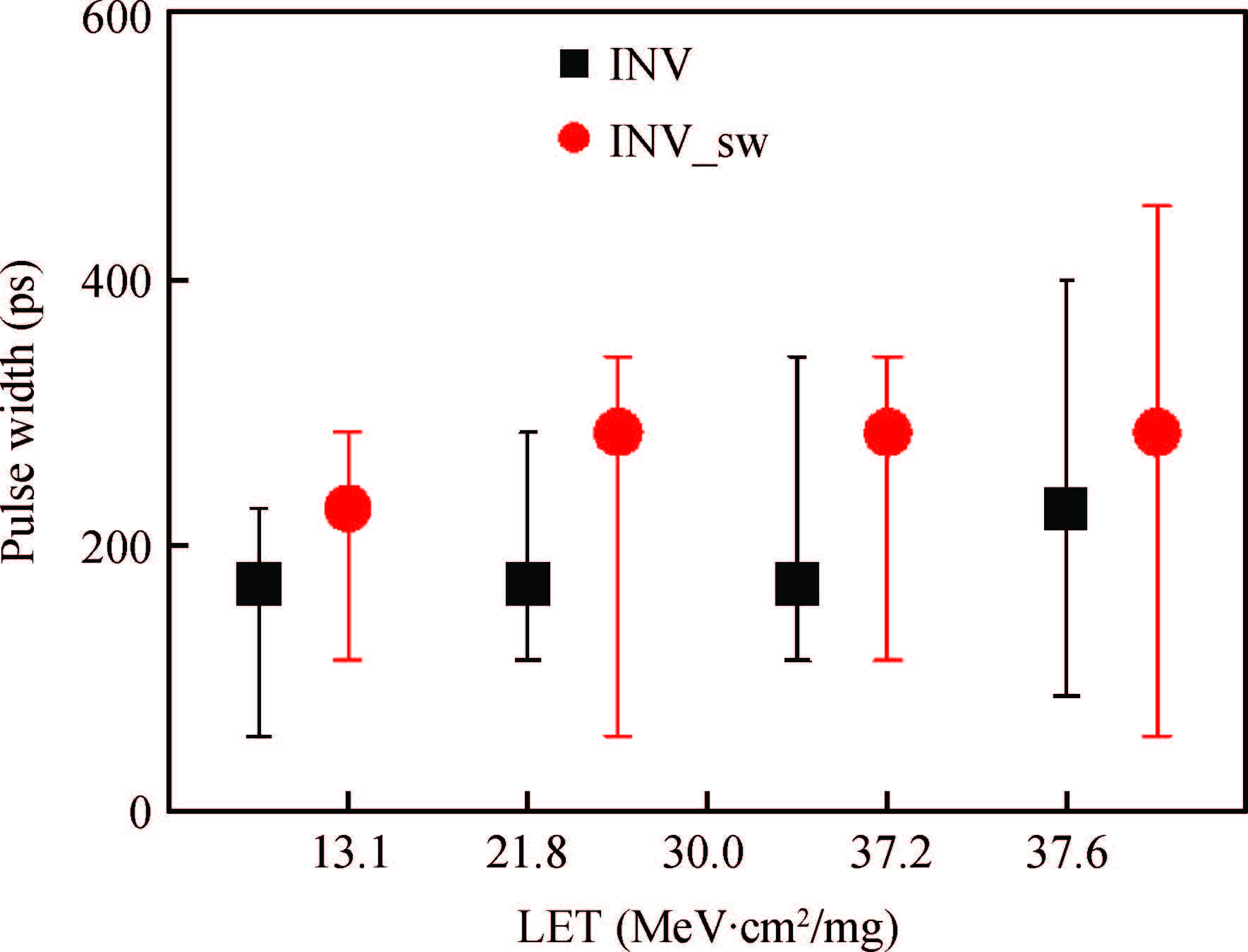
Heavy ion results of a 65-nm CMOS SET pulse width testchip are given. The influences of device threshold voltage, temperature and well separation on pulse width are discussed. Experimental data implied that the low device threshold, high temperature and well speraration would contribute to wider SET. The multi-peak phenomenon in the distribution of SET pulse width was first observed and its dependence on various factors is also discussed.

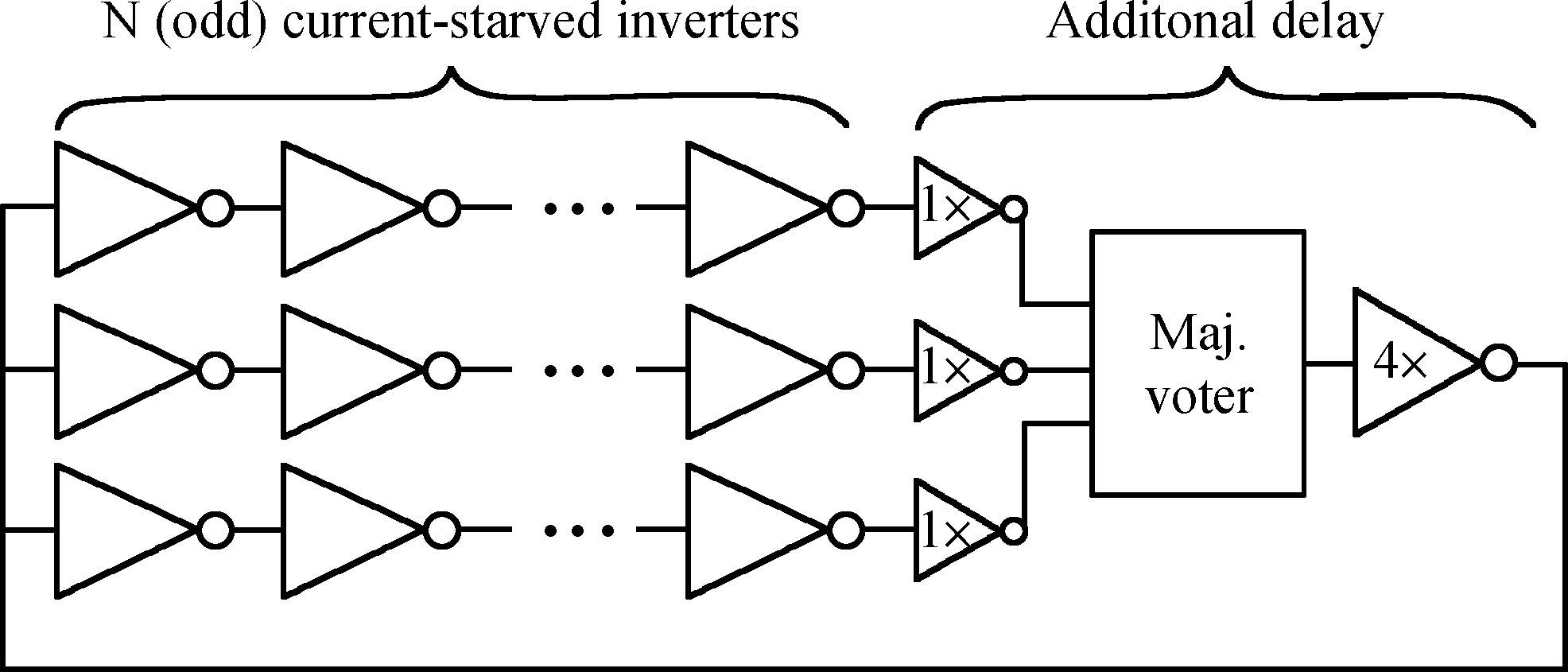
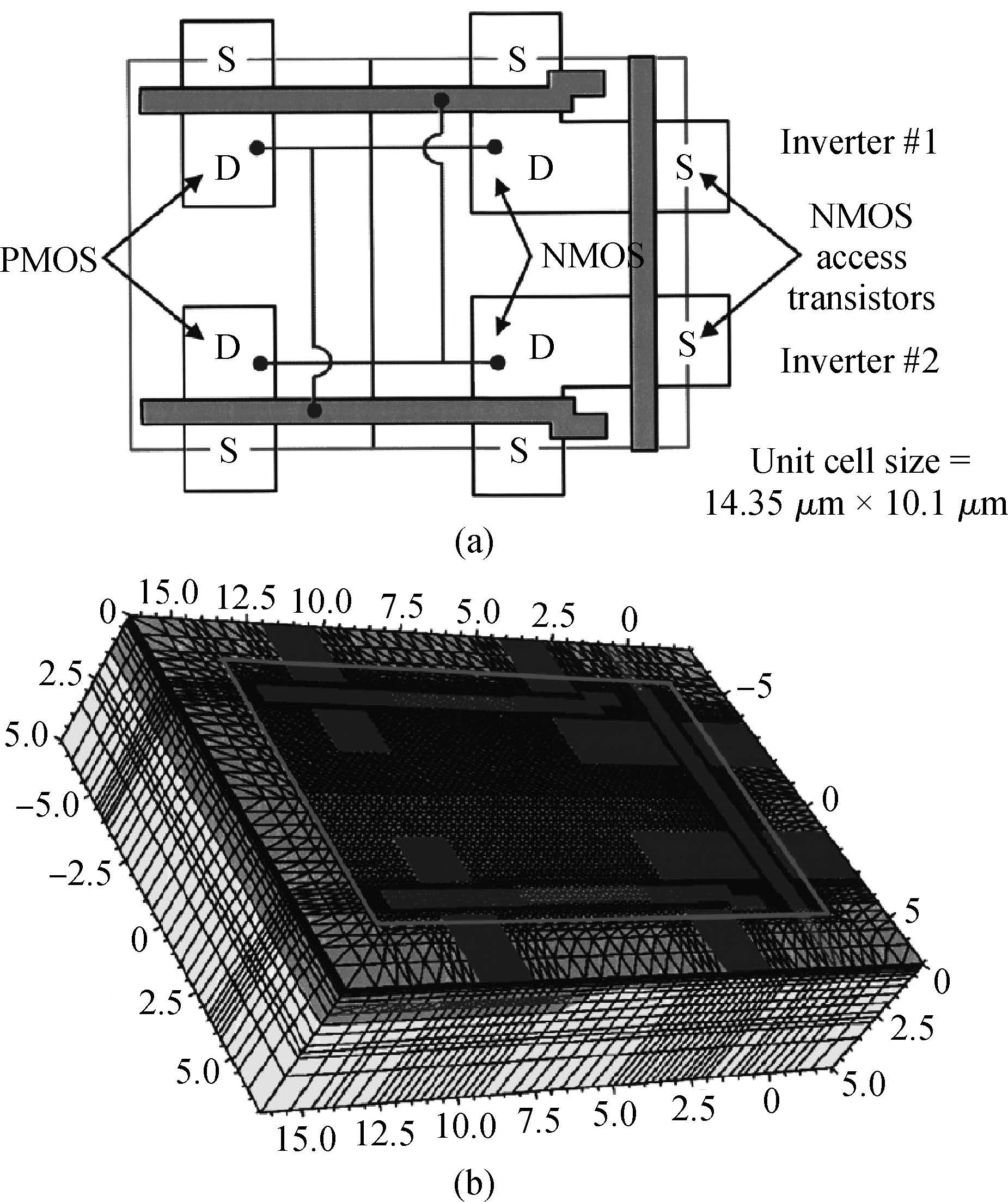
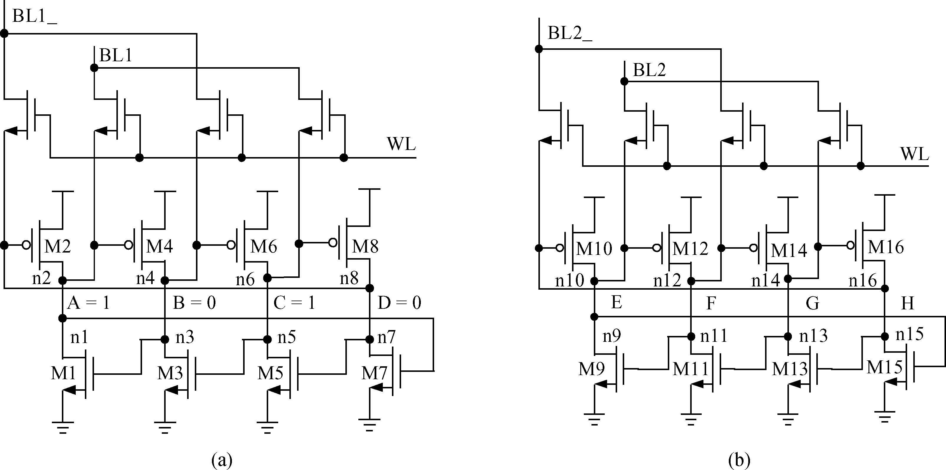
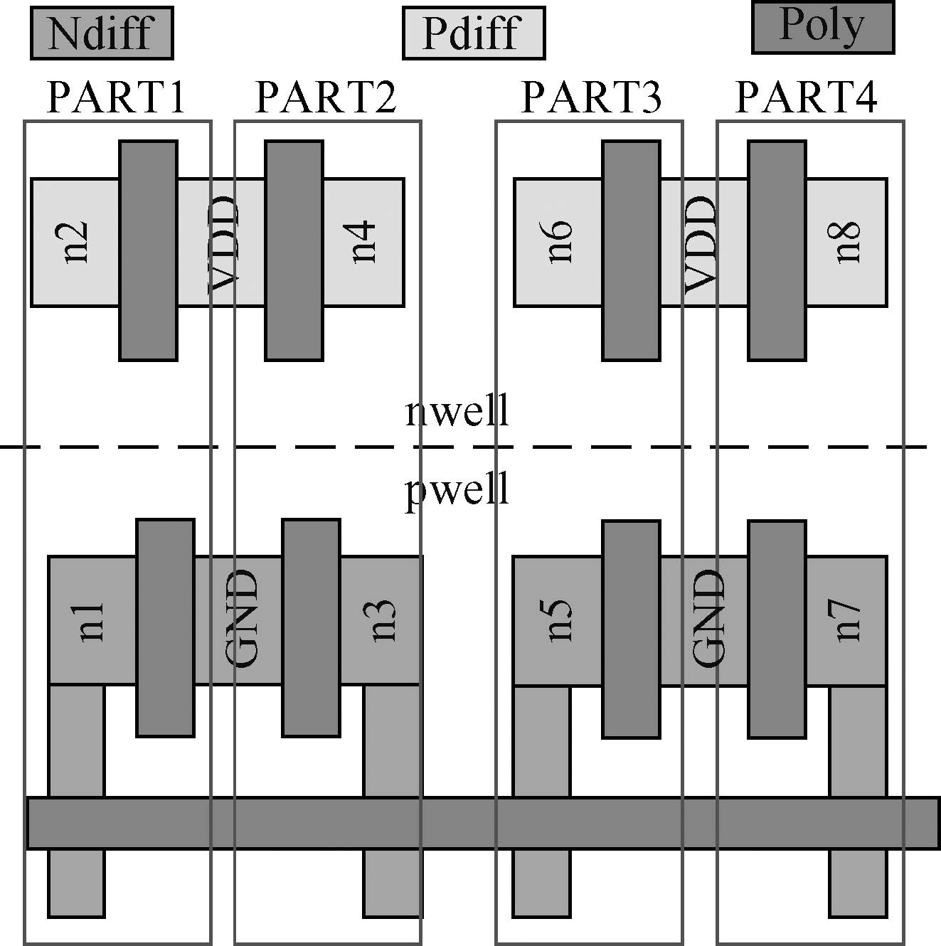
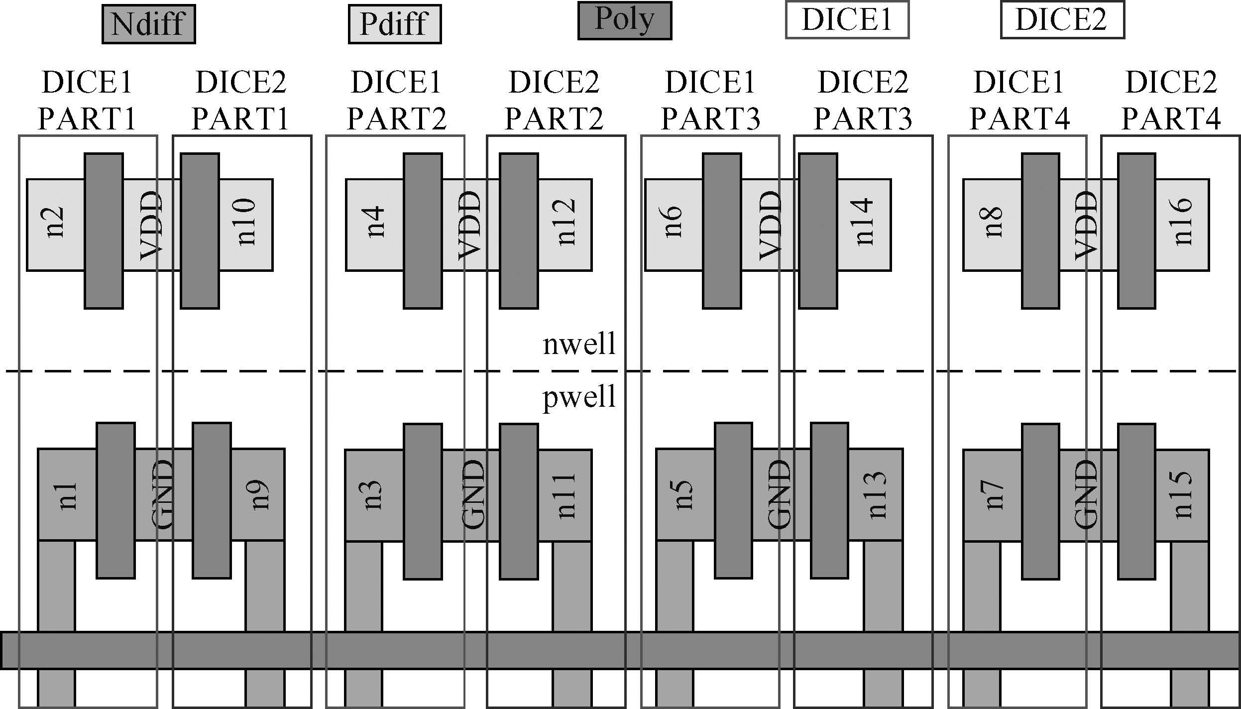
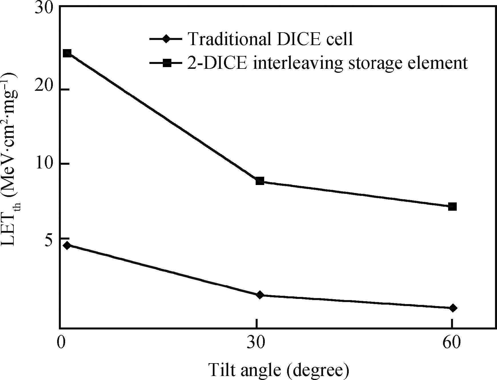
A 4-interleaving cell of 2-dual interlocked cells (DICE) is proposed, which reduces single event induced multiple node collection between the sensitive nodes of sensitive pairs in a DICE storage cell in 65 nm technology. The technique involves the 4-interleaving of dual DICE cells at a layout level to meet the required spacing between sensitive nodes in an area-efficient manner. Radiation experiments using a 65 nm CMOS test chip demonstrate that the LETth of our 4-interleaving cell of dual DICE encounters are almost 4× larger and the SEU cross section per bit for our proposed dual DICE design is almost two orders of magnitude less compared to the reference traditional DICE cell.

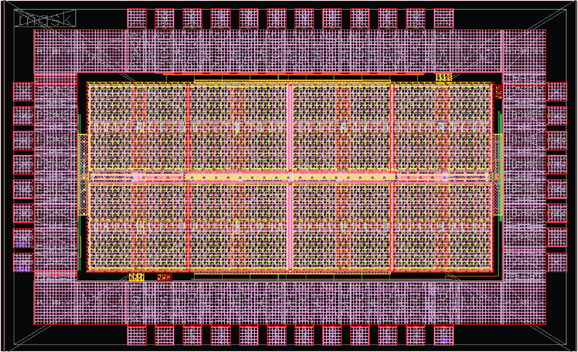

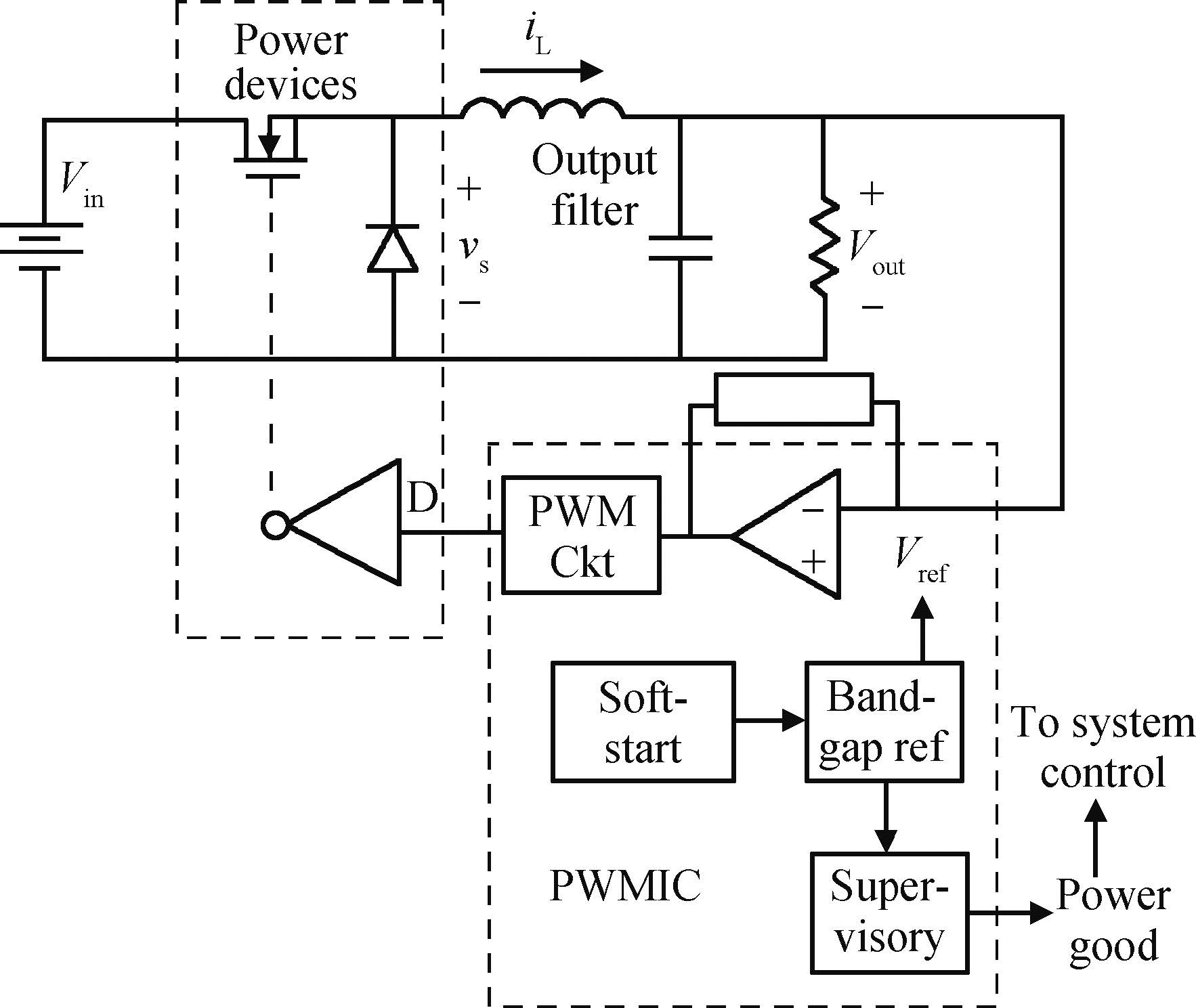
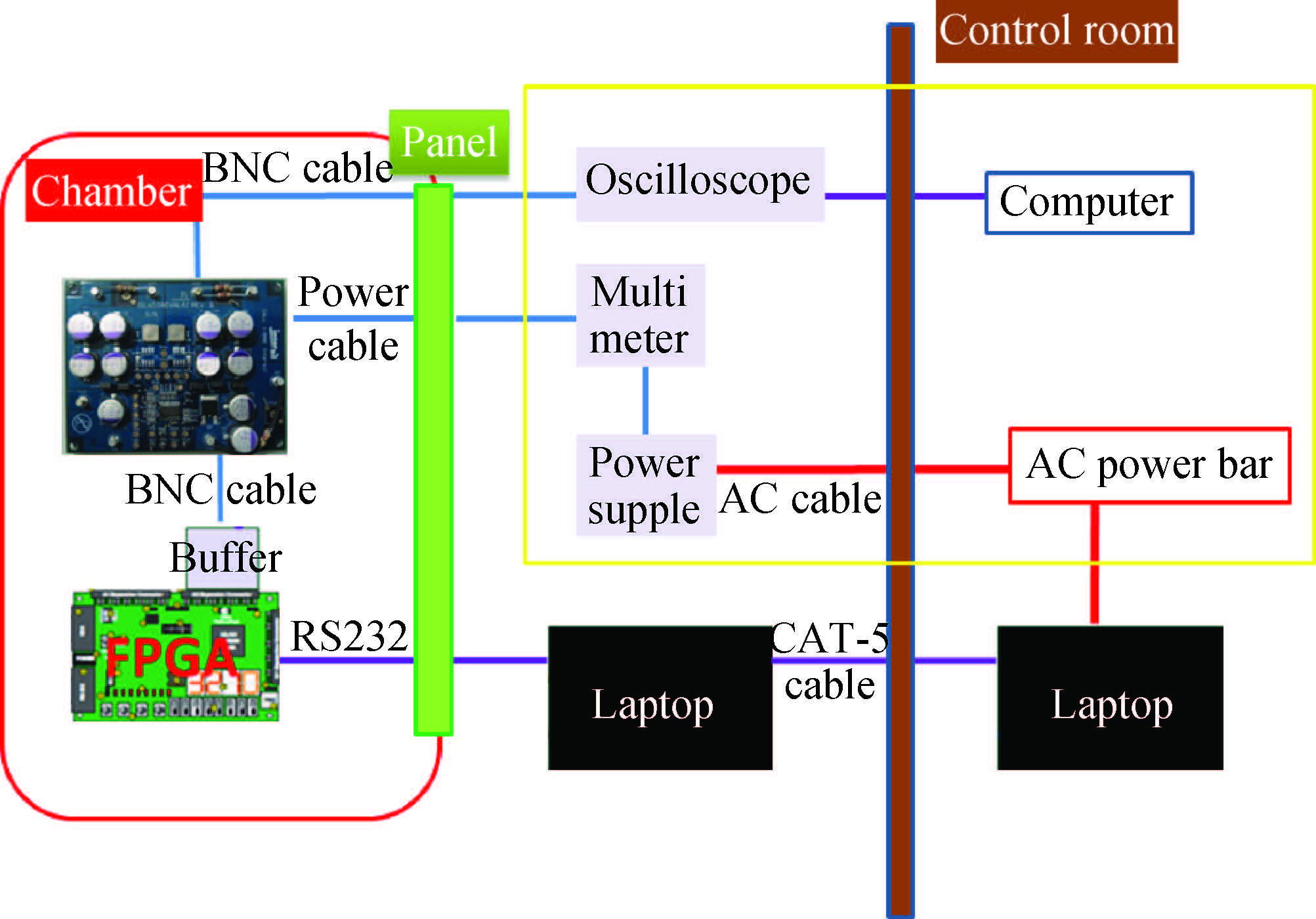
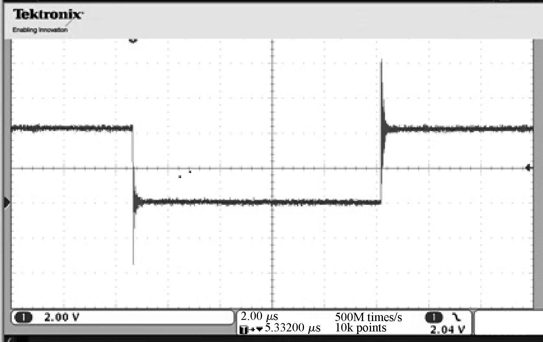
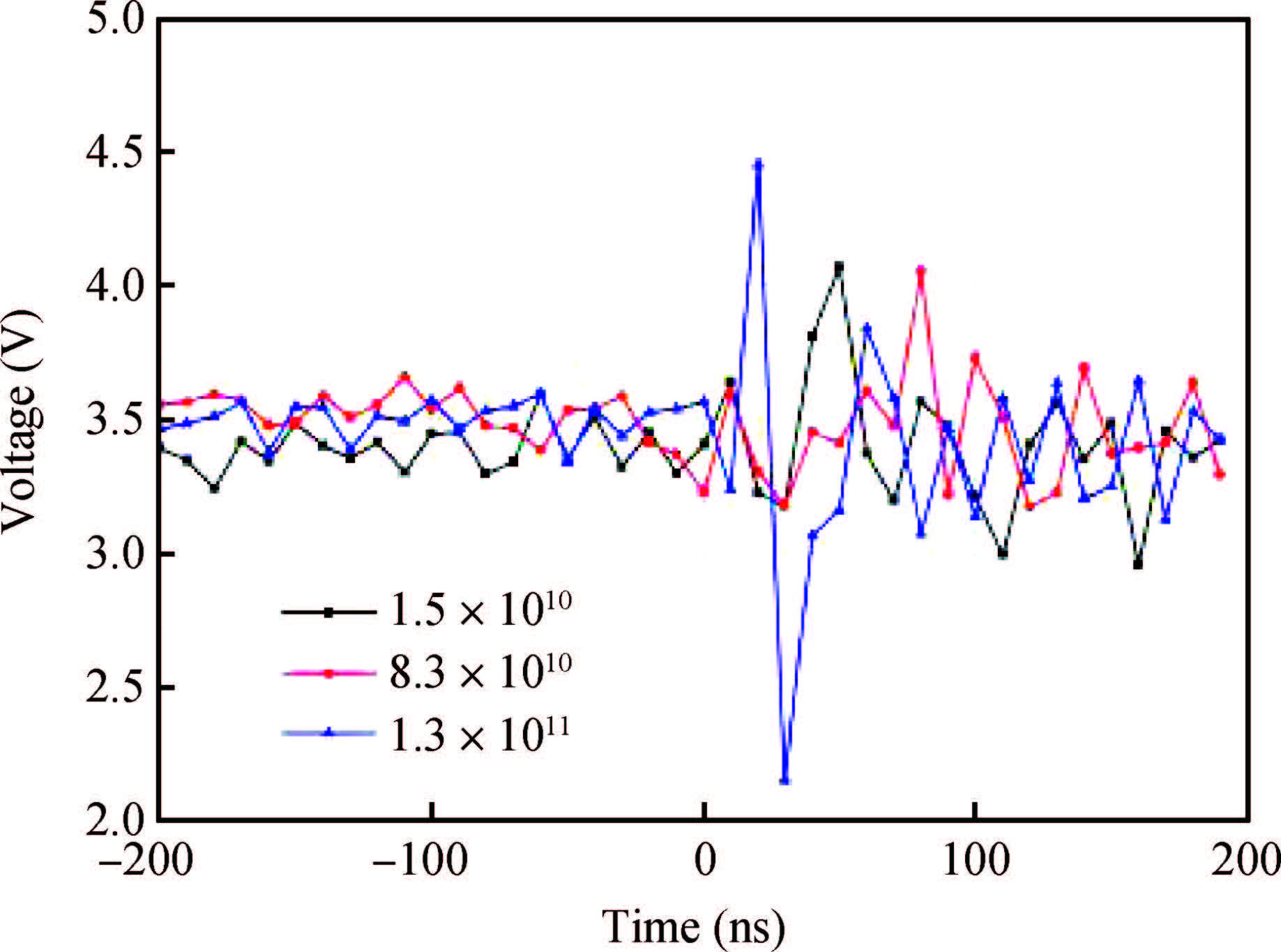
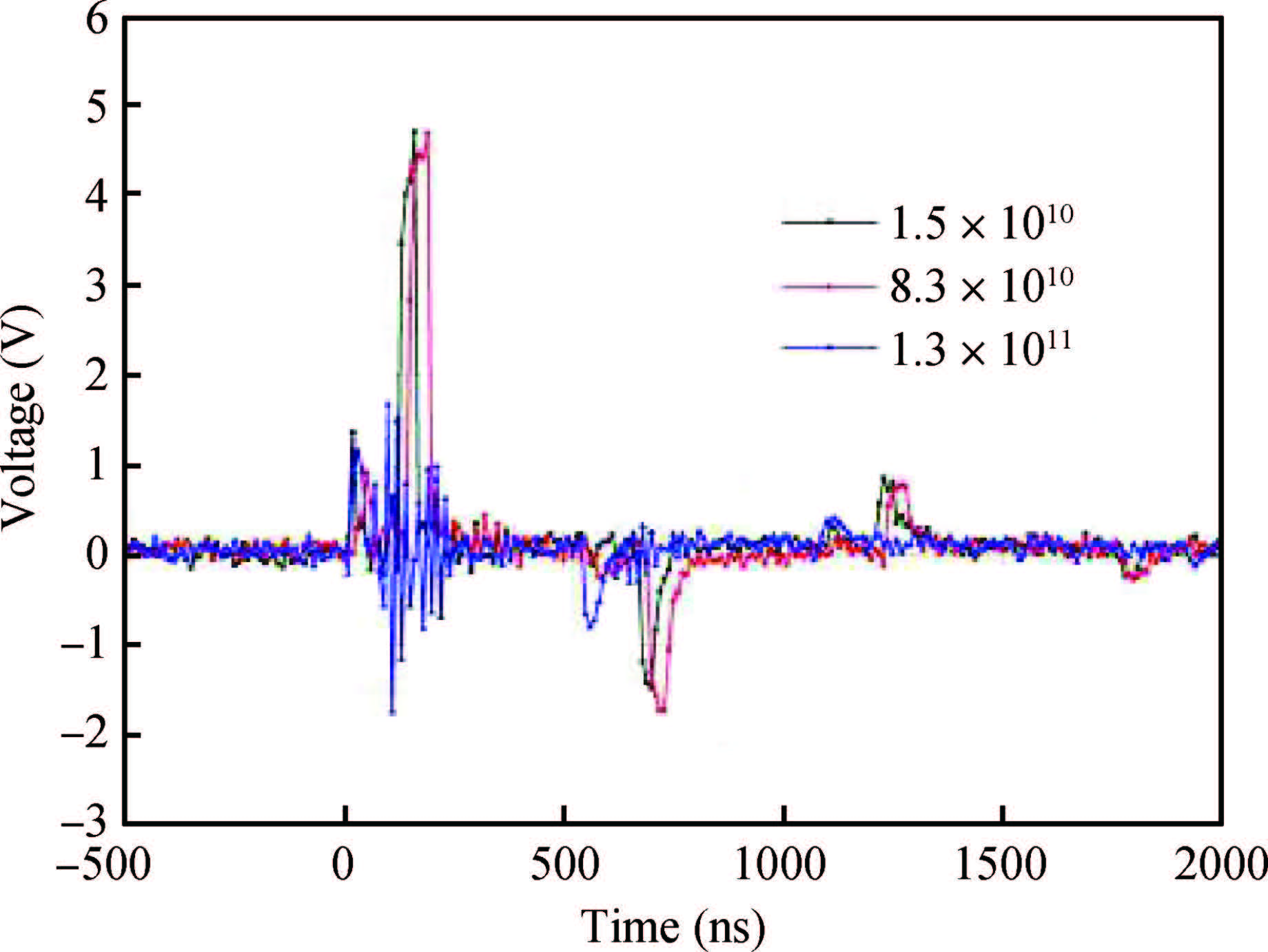
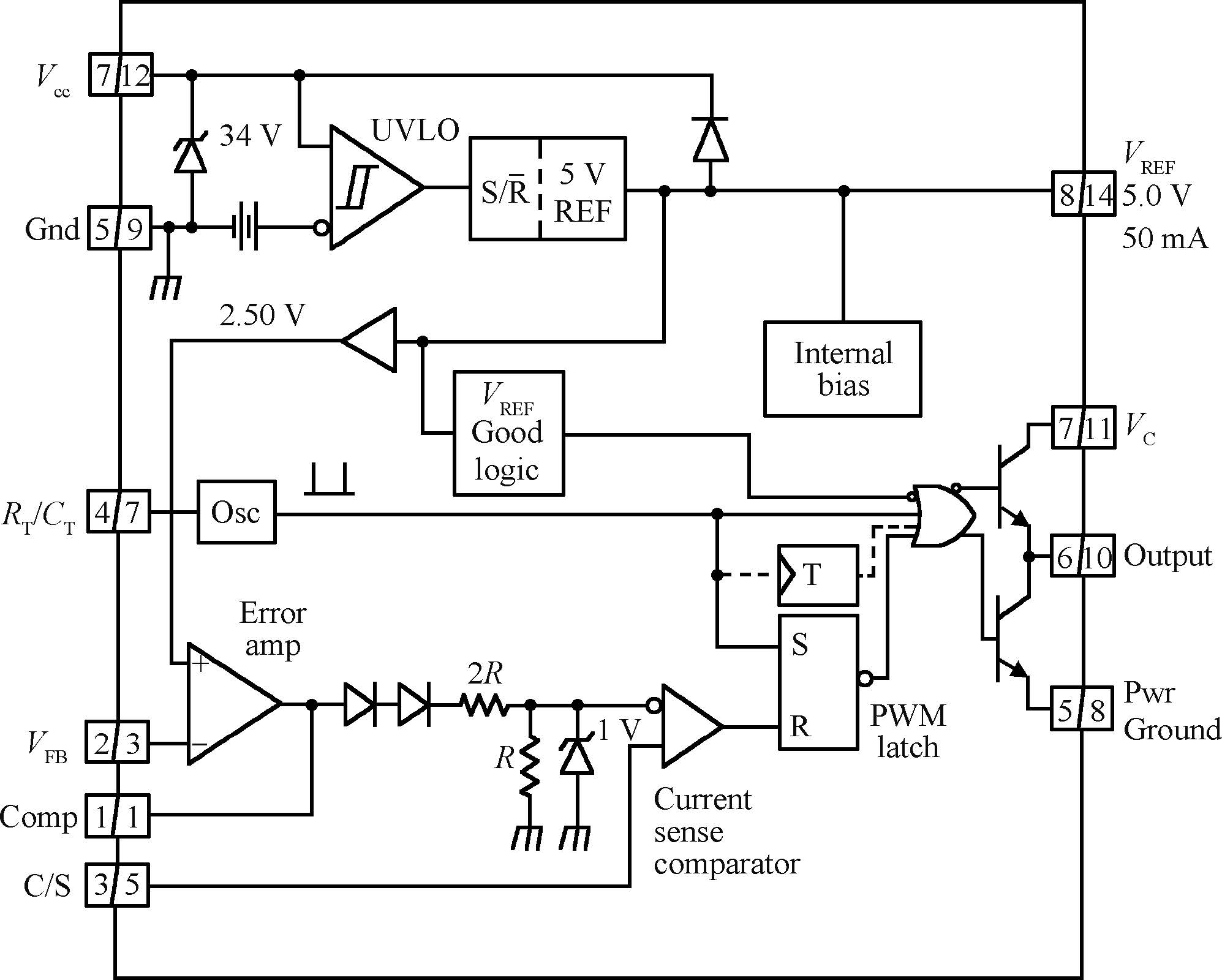
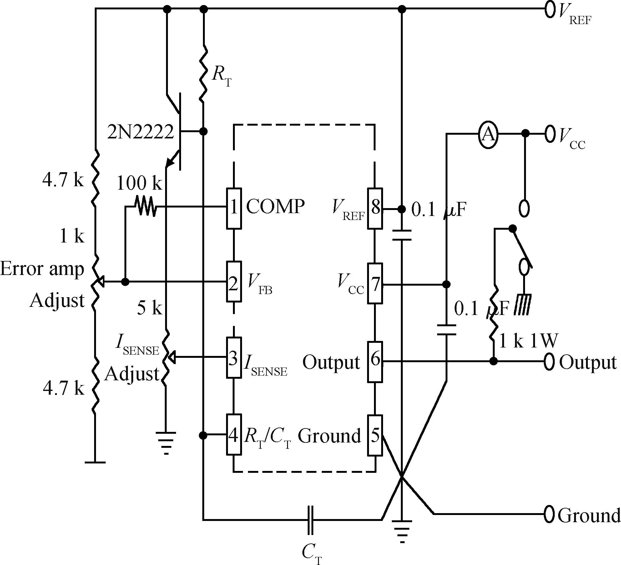
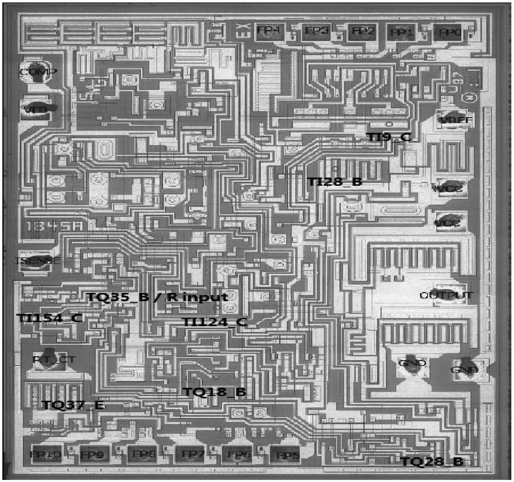
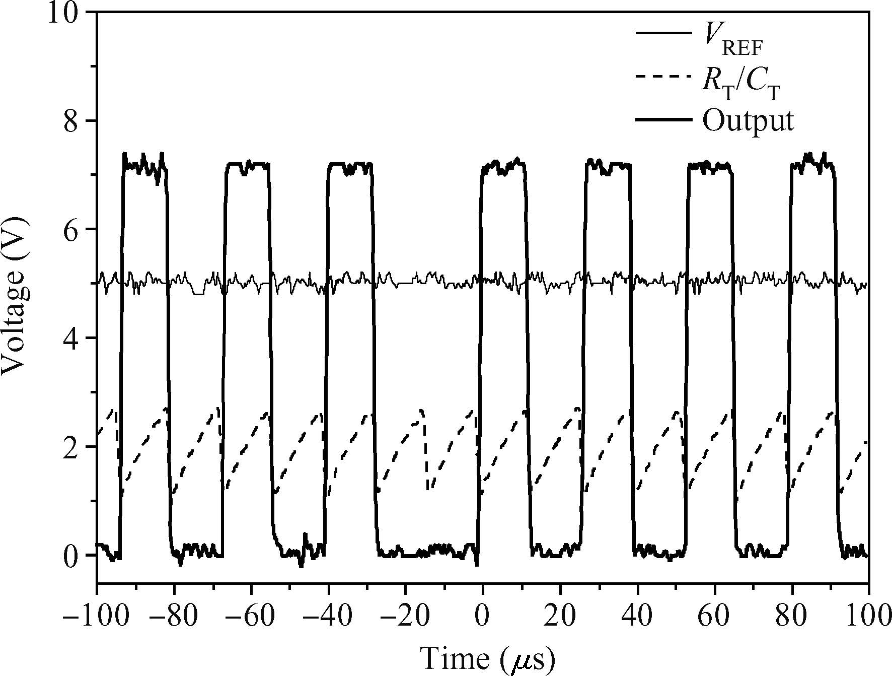
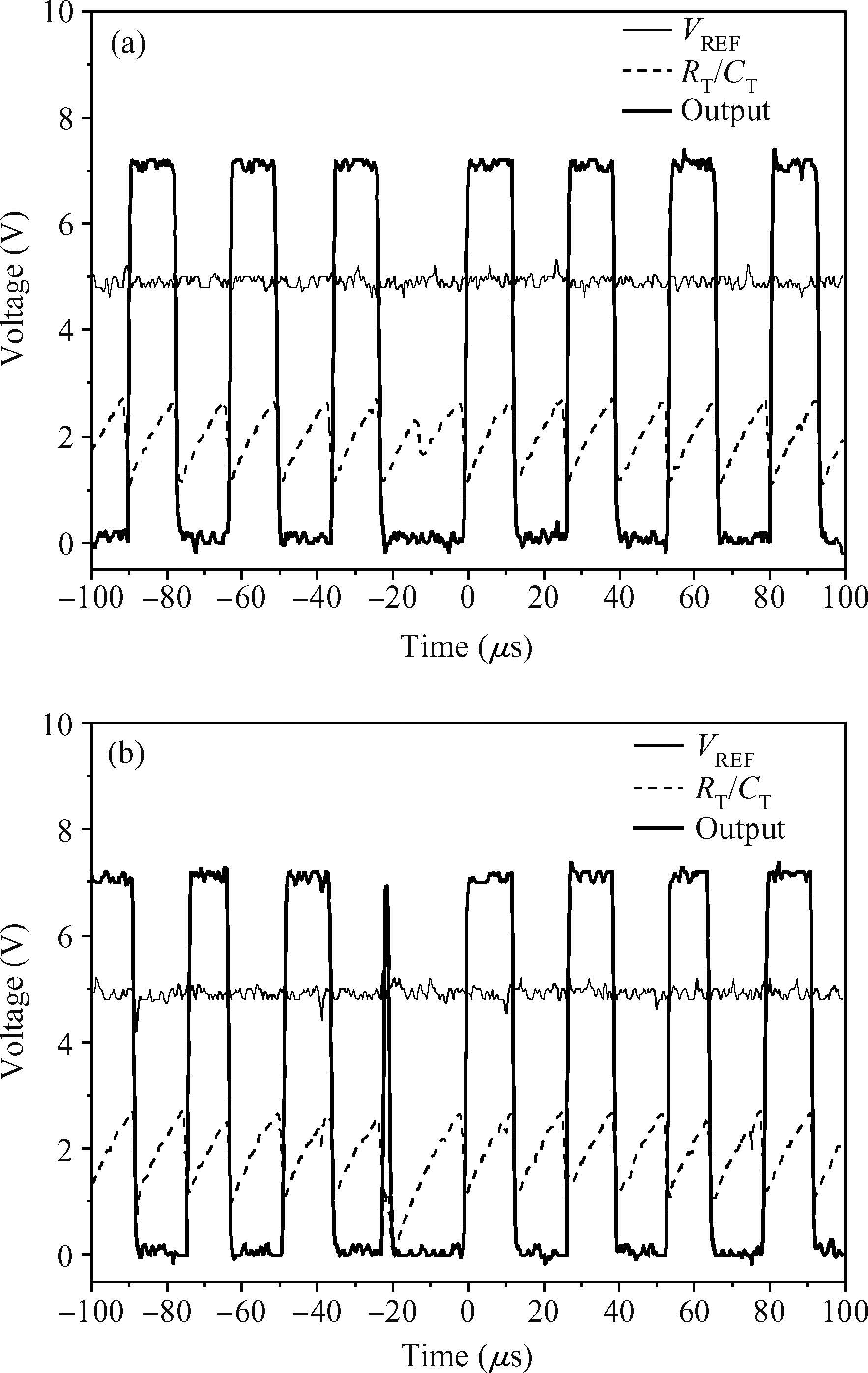
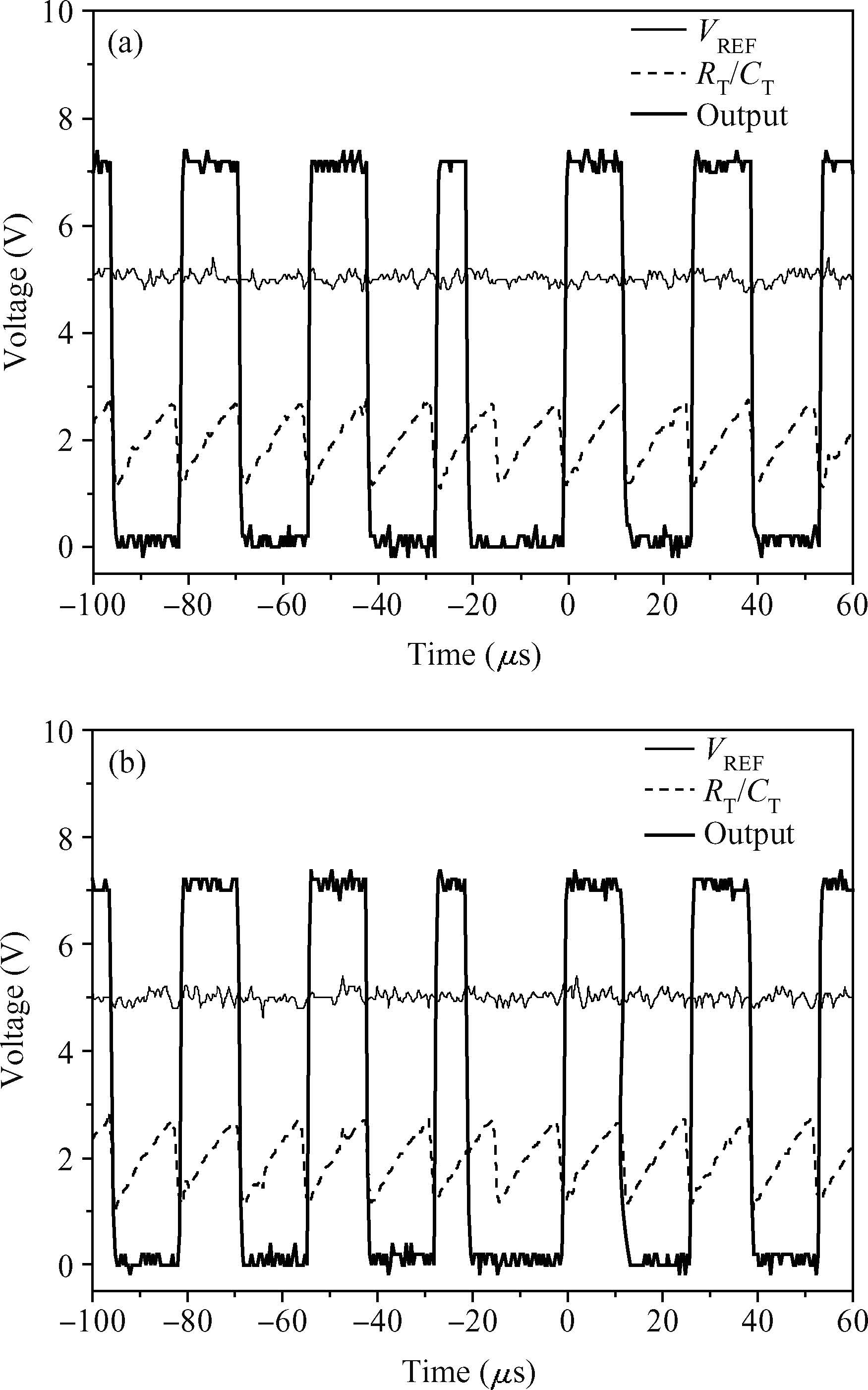
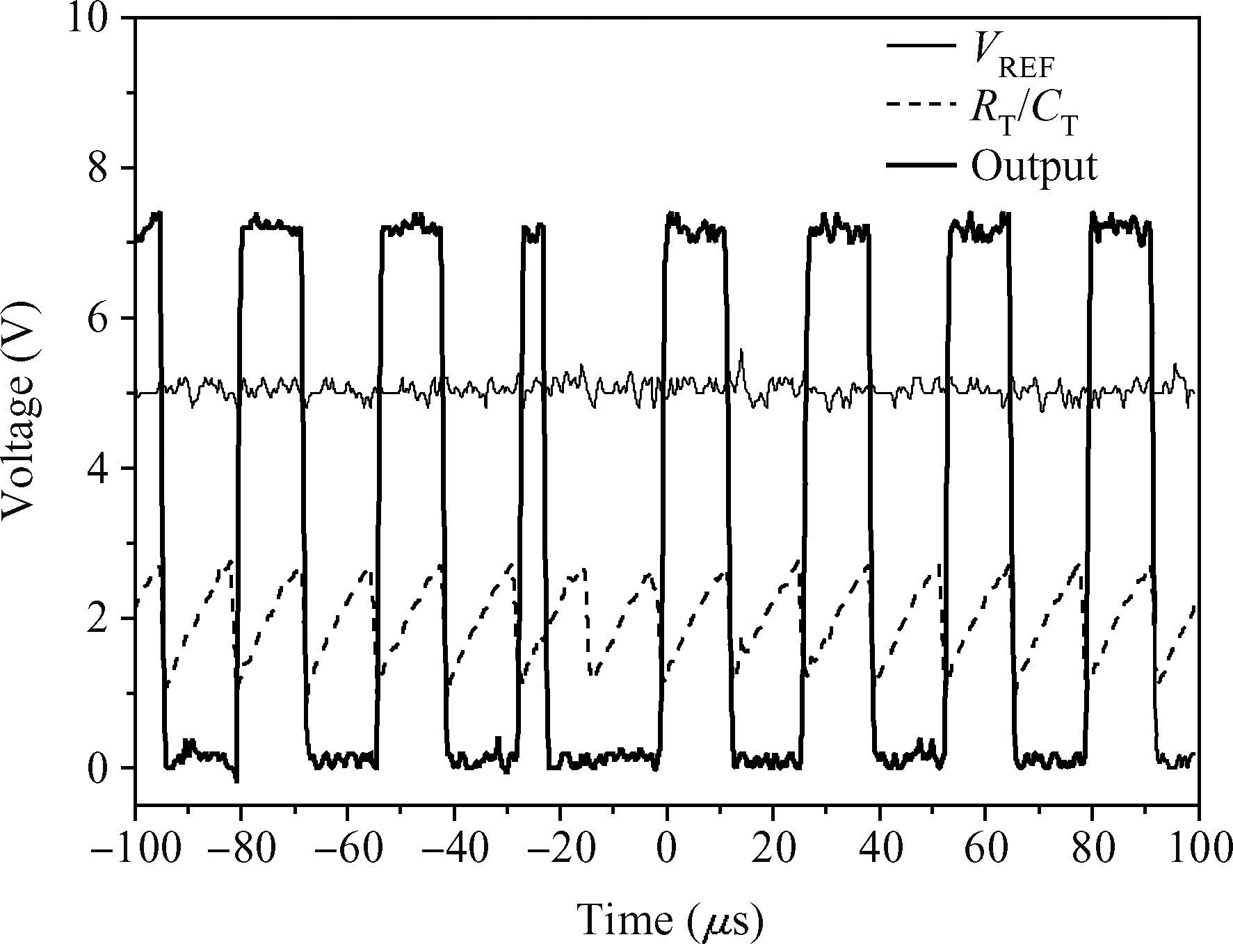
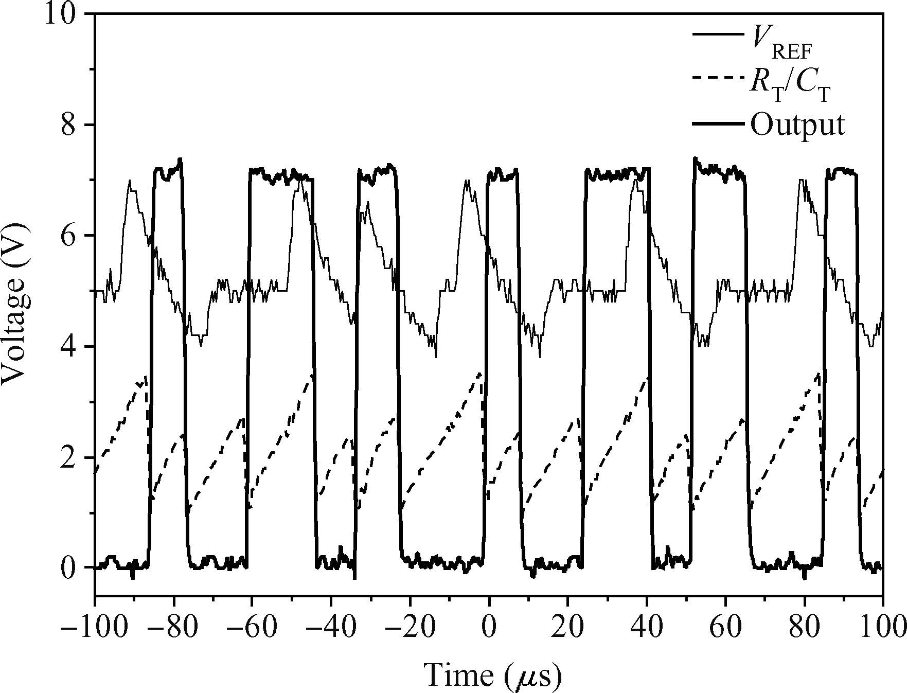
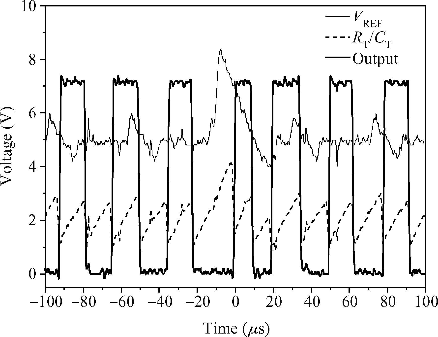
This paper presents single event effect (SEE) characteristics of UC1845AJ pulse width modulators (PWMs) by laser testing. In combination with analysis to map PWM circuitry in the microchip dies, the typical SEE response waveforms for laser pulses located in different circuit blocks of UC1845AJ are obtained and the SEE mechanisms are analyzed. The laser SEE test results show that there are some differences in the SEE mechanisms of different circuit blocks, and phase shifts or changes in the duty cycles of few output pulses are the main SEE behaviors for UC1845AJ. In addition, a new SEE behavior which manifests as changes in the duty cycles of many output pulses is revealed. This means that an SEE hardened design should be considered.

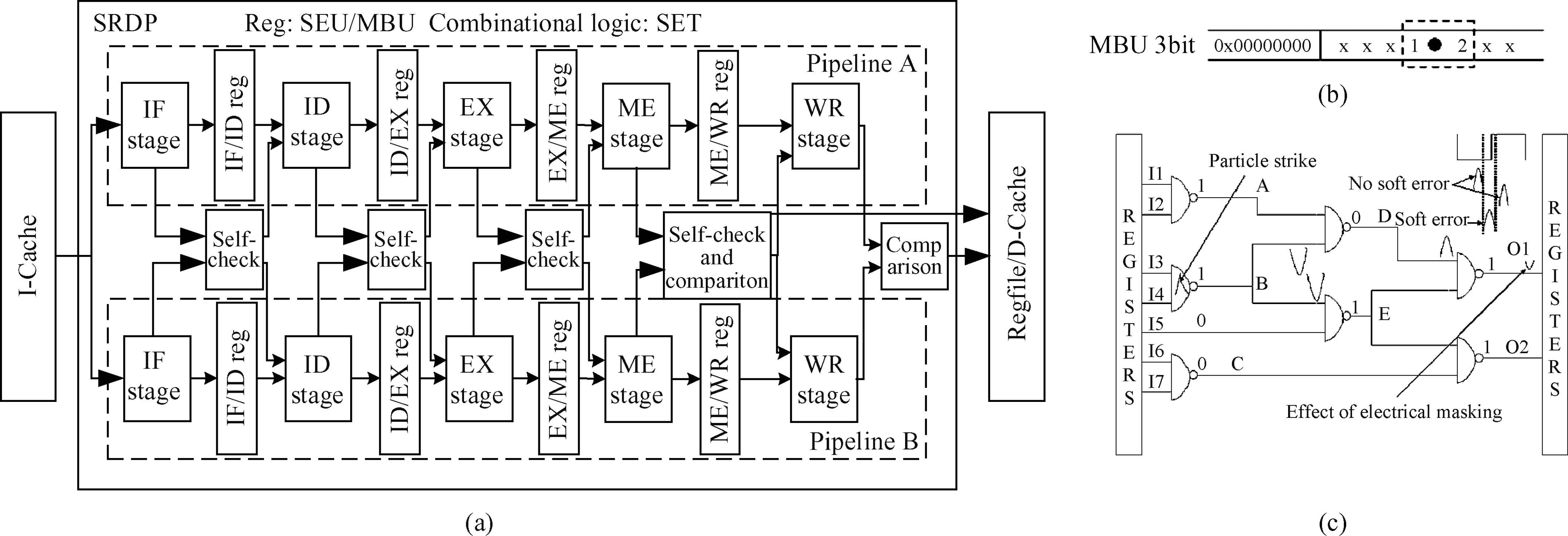
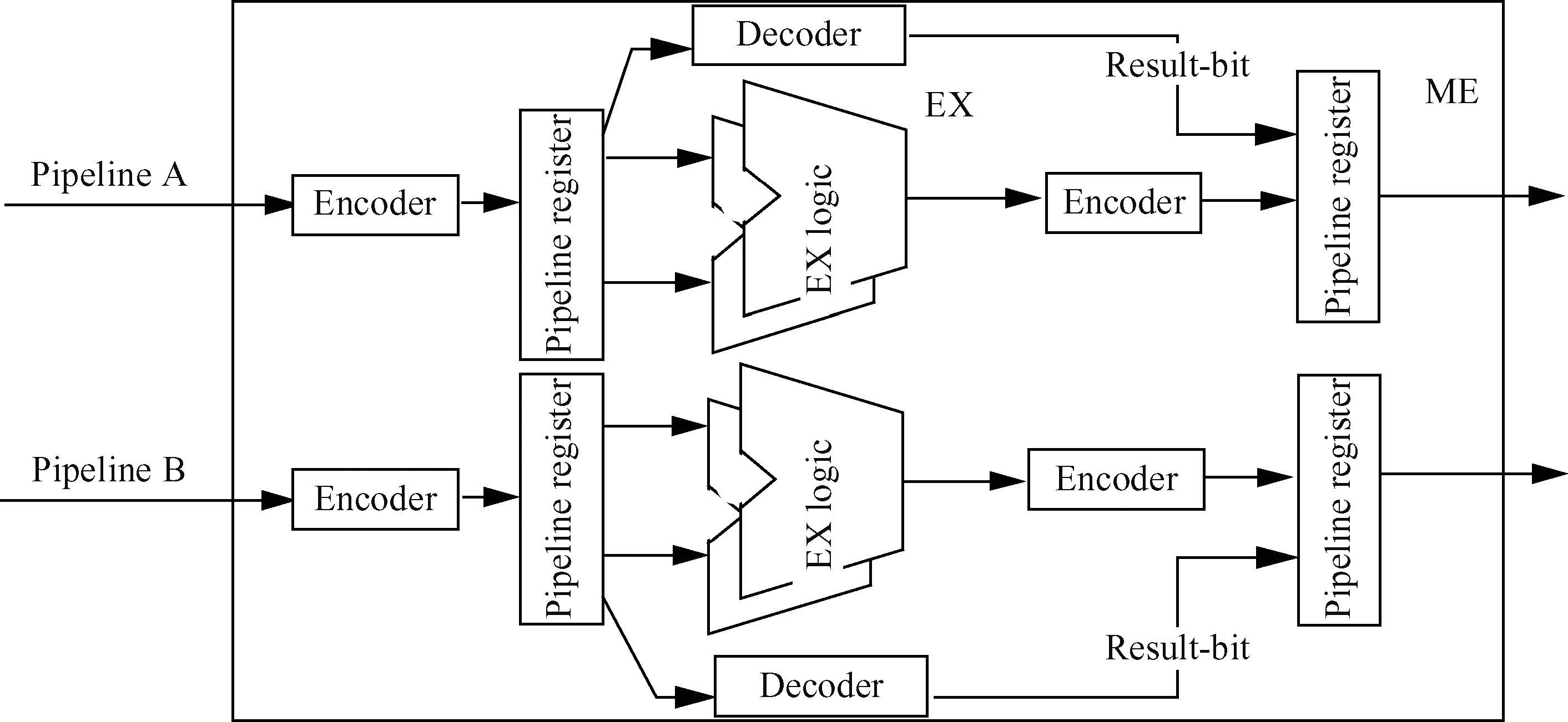
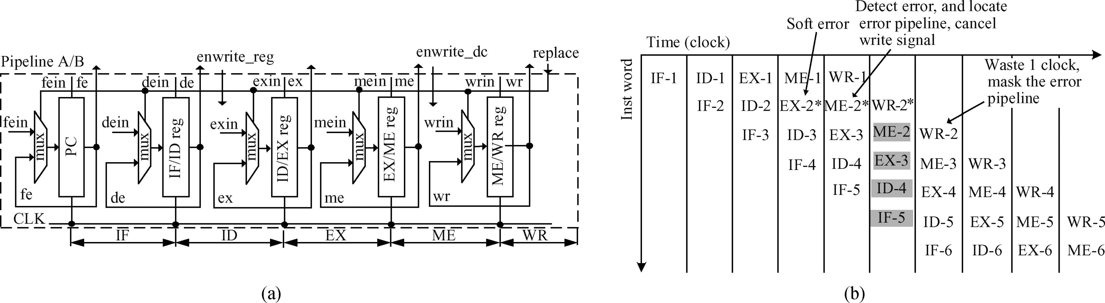
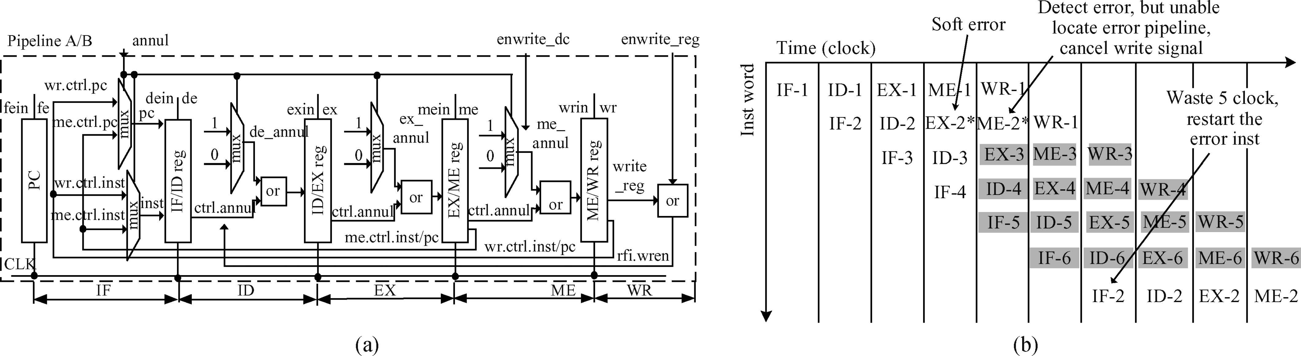
The particles-induced soft errors are a major threat to the reliability of microprocessors. Even worse, multi-bits upsets (MBUs) are ever-increased due to the rapidly shrinking feature size of the IC on a chip. Several architecture-level mechanisms have been proposed to protect microprocessors from soft errors, such as dual and triple modular redundancies (DMR and TMR). However, most of them are inefficient to combat the growing multi-bits errors or cannot well balance the critical paths delay, area and power penalty. This paper proposes a novel architecture, self-recovery dual-pipeline (SRDP), to effectively provide soft error detection and recovery with low cost for general RISC structures. We focus on the following three aspects. First, an advanced DMR pipeline is devised to detect soft error, especially MBU. Second, SEU/MBU errors can be located by enhancing self-checking logic into pipelines stage registers. Third, a recovery scheme is proposed with a recovery cost of 1 or 5 clock cycles. Our evaluation of a prototype implementation exhibits that the SRDP can successfully detect particle-induced soft errors up to 100% and recovery is nearly 95%, the other 5% will inter a specific trap.


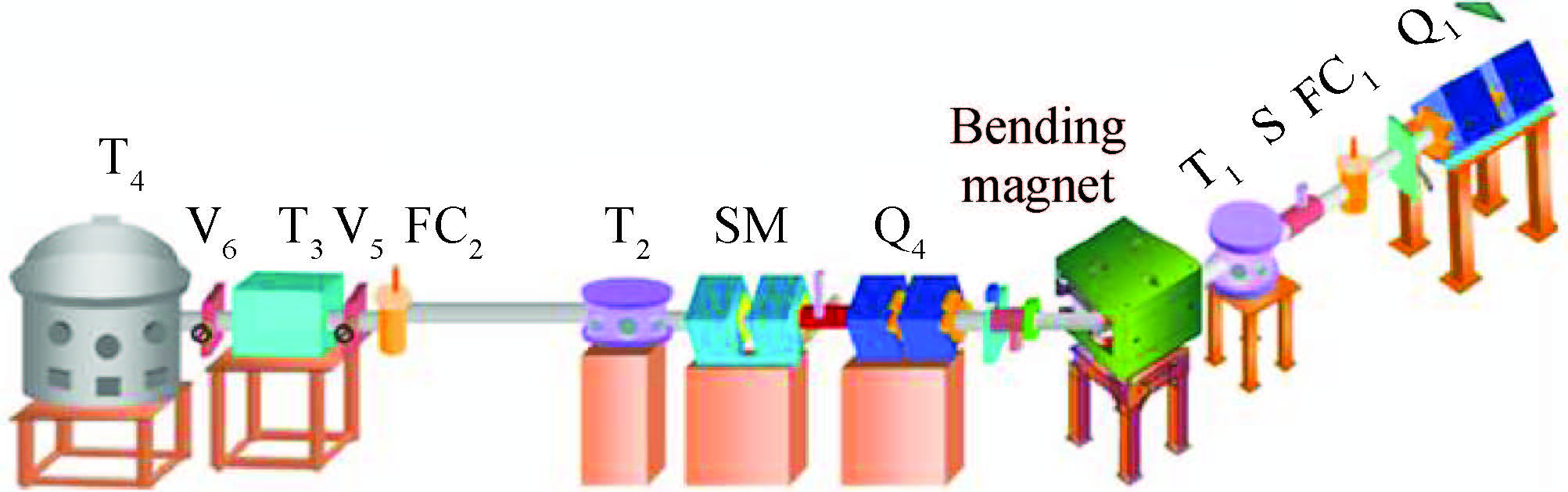
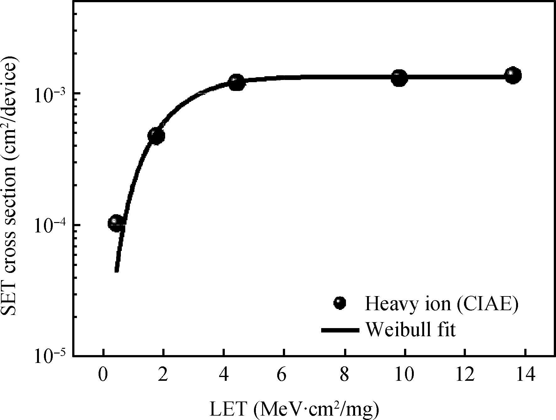
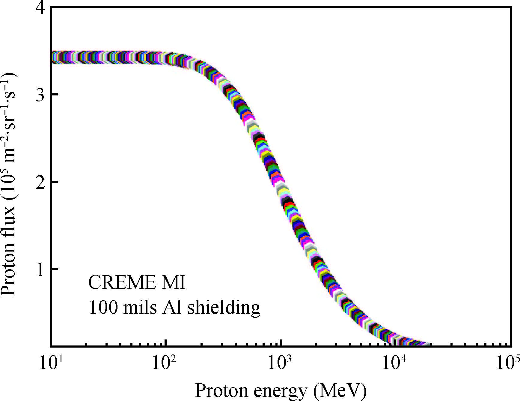
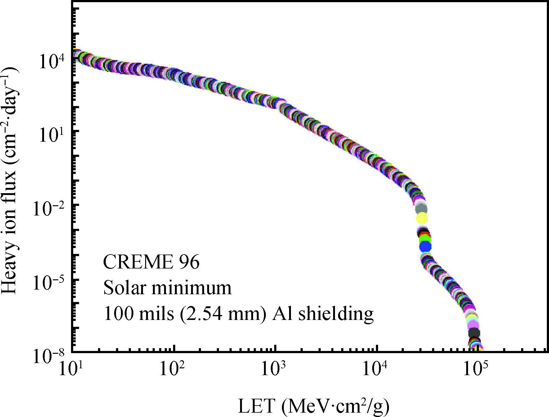
This paper tested and analyzed heavy ion and proton induced single event effects (SEE) of a commercial DC/DC converter based on a 600 nm Bi-CMOS technology. Heavy ion induced single event transients (SET) testing has been carried out by using the Beijing HI-13 tandem accelerator at China Institute of Atomic Energy. Proton test has been carried out by using the Canadian TRIUMF proton accelerator. Both SET cross section versus linear energy transfer (LET) and proton energy has been measured. The main study conclusions are: (1) the DC/DC is both sensitive to heavy ion and proton radiations although at a pretty large feature size (600 nm), and threshold LET is about 0.06 MeV·mg/cm2; (2) heavy ion SET saturation cross section is about 5 magnitudes order larger than proton SET saturation cross section, which is consistent with the theory calculation result deduced by the RPP model and the proton nuclear reaction model; (3) on-orbit soft error rate (SER) prediction showed, on GEO orbit, proton induced SERs calculated by the heavy ion derived model are 4-5 times larger than those calculated by proton test data.