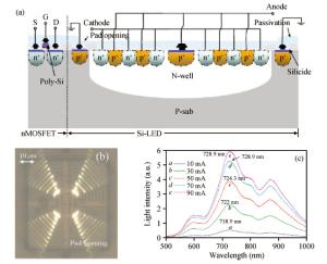
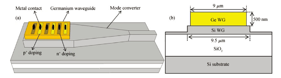
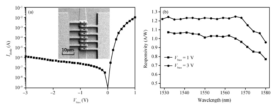
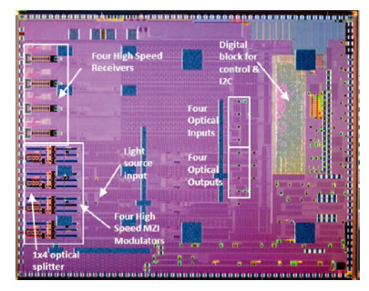
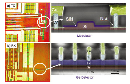
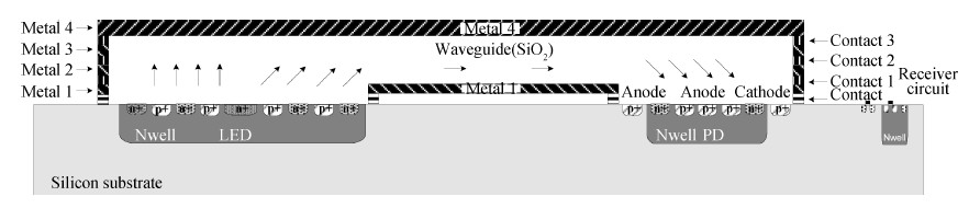
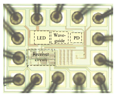
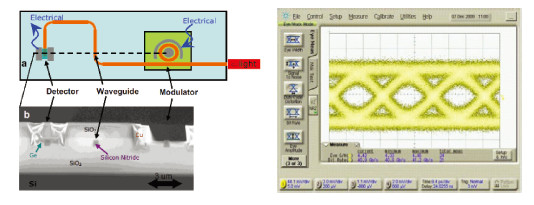
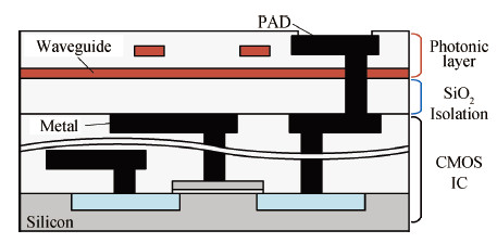
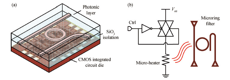
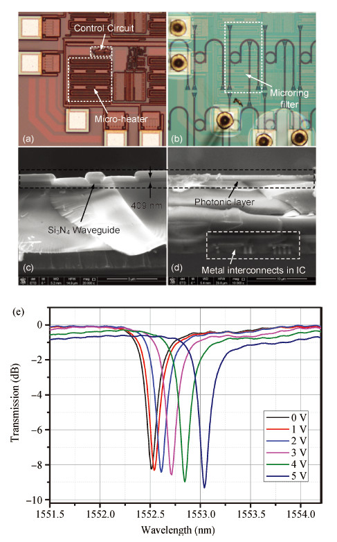
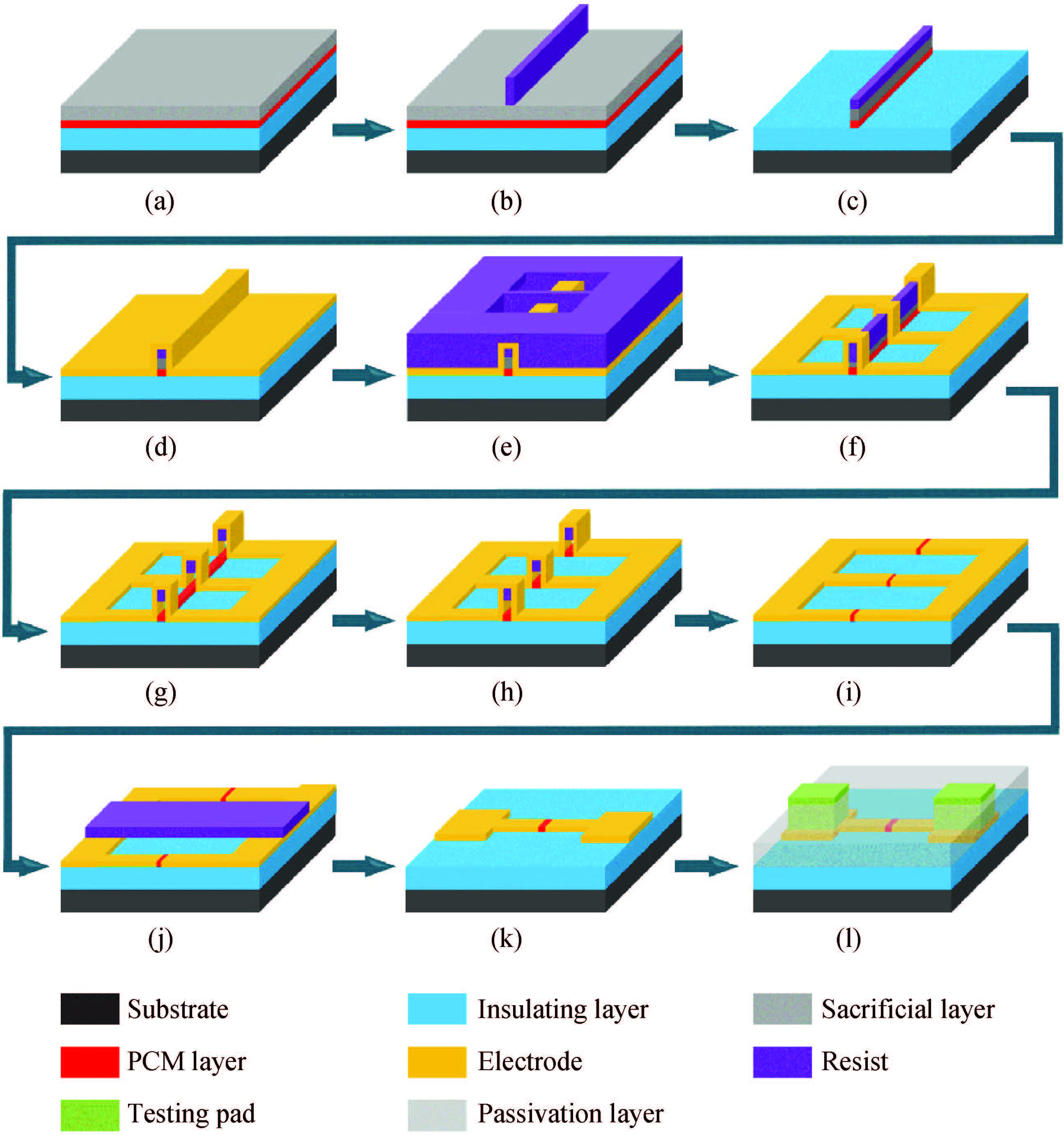
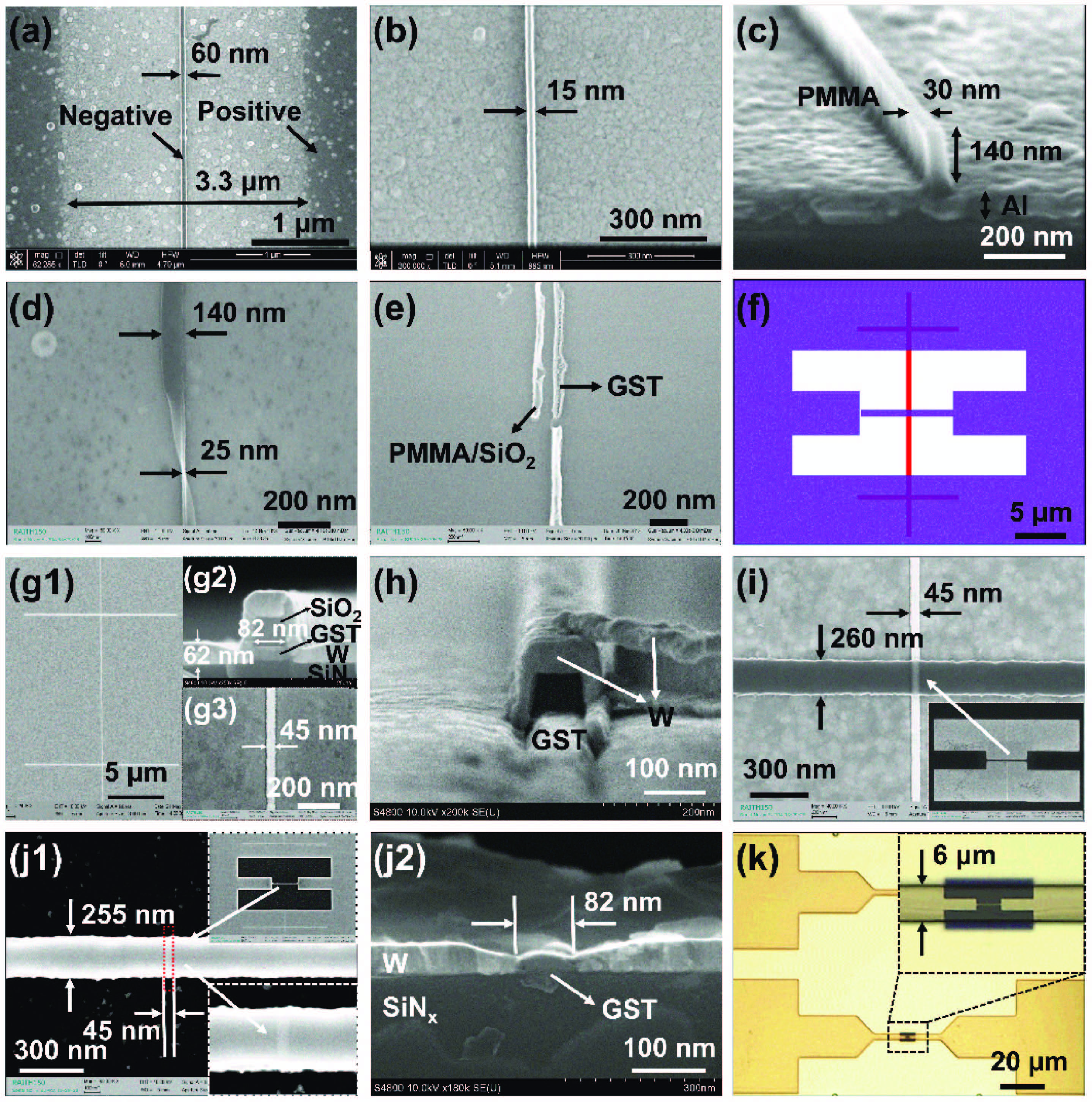
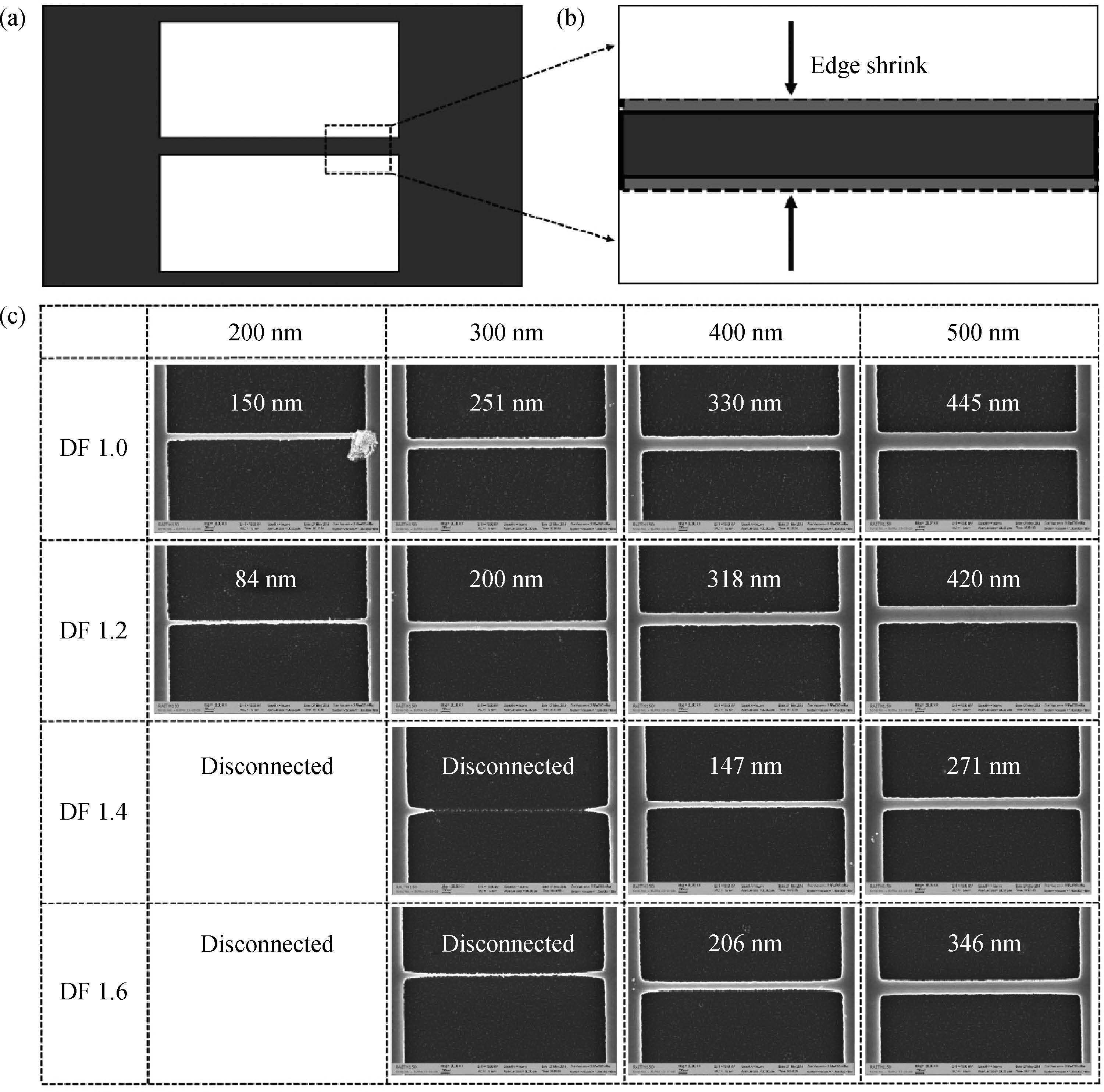
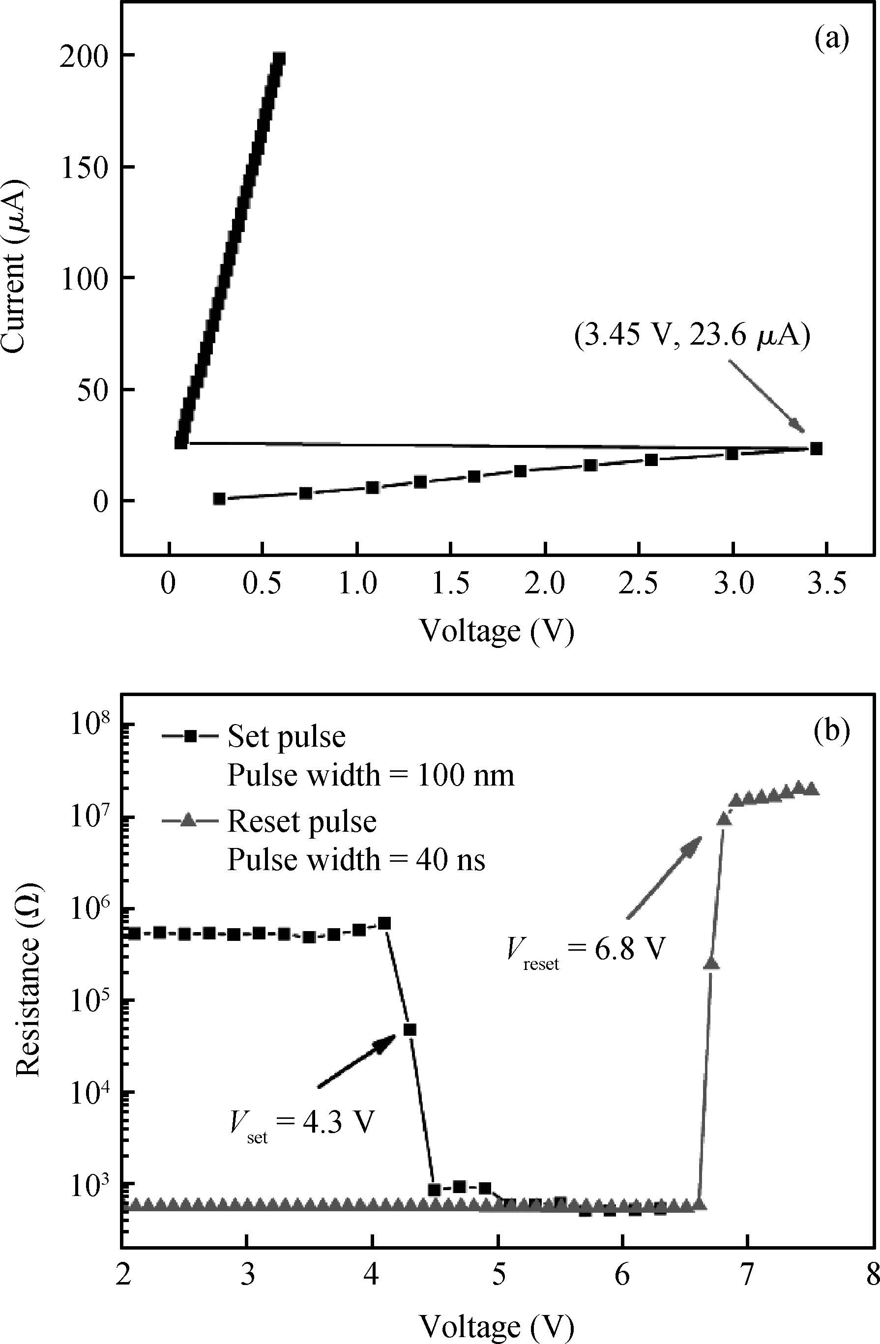
Silicon photonics is an emerging competitive solution for next-generation scalable data communications in different application areas as high-speed data communication is constrained by electrical interconnects. Optical interconnects based on silicon photonics can be used in intra/inter-chip interconnects, board-to-board interconnects, short-reach communications in datacenters, supercomputers and long-haul optical transmissions. In this paper, we present an overview of recent progress in silicon optoelectronic devices and optoelectronic integrated circuits(OEICs) based on a complementary metal-oxide-semiconductor-compatible process, and focus on our research contributions. The silicon optoelectronic devices and OEICs show good characteristics, which are expected to benefit several application domains, including communication, sensing, computing and nonlinear systems.


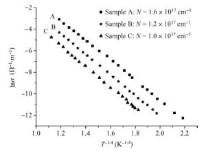
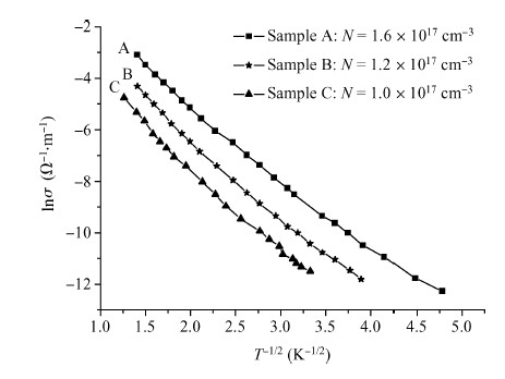
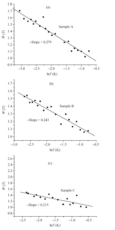
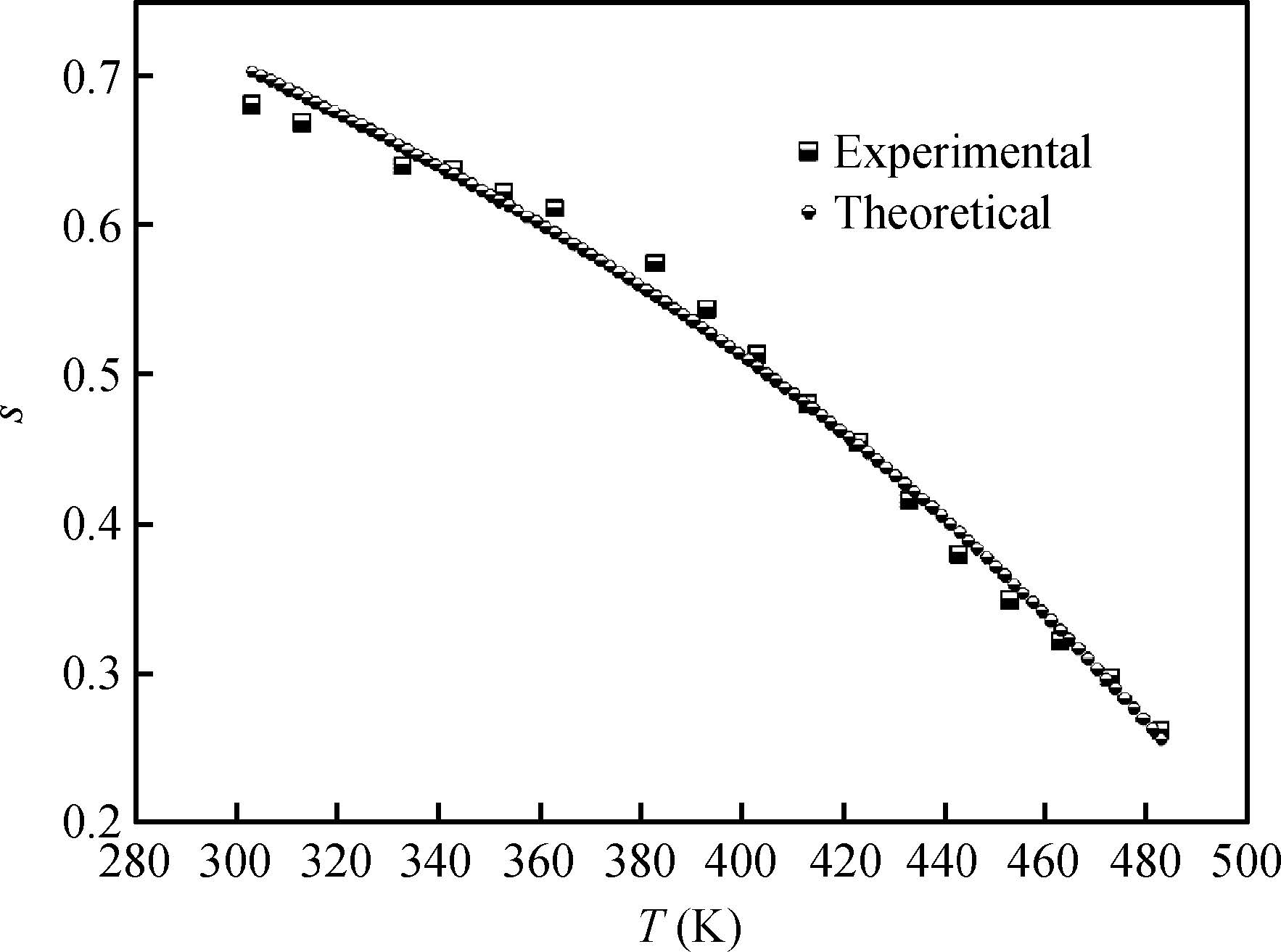
We reanalyzed experimental data already published in Friedman J R, Zhang Y, Dai P, et al. Phys Rev B, 1996, 53(15):9528. Variable range hopping(VRH) conduction in the insulating three-dimensional n-CdSe samples has been studied over the entire temperature range from 0.03 to 1 K. In the absence of a magnetic field, the low temperature conductivity σ of the three samples(A, B and C) obeys the Mott VRH conduction with an appropriate temperature dependence in the prefactor(σ=σ0 exp[-(T0/T)p with p≈0.25). This behavior can be explained by a VRH model where the transport occurs by hopping between localized states in the vicinity of the Fermi level, EF, without creation of the Coulomb gap(CG). On the contrary, no Efros-Shklovskii VRH is observed, suggesting that the density is constant in the vicinity of the EF.

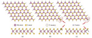
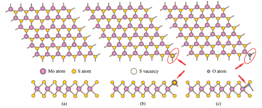
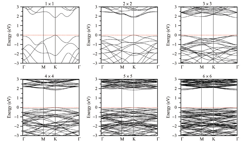
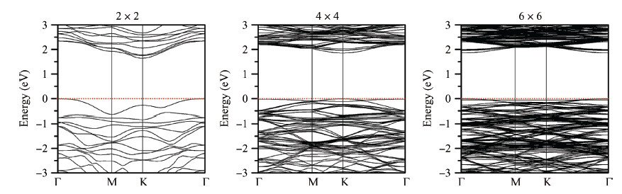
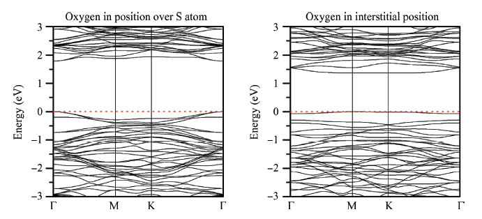
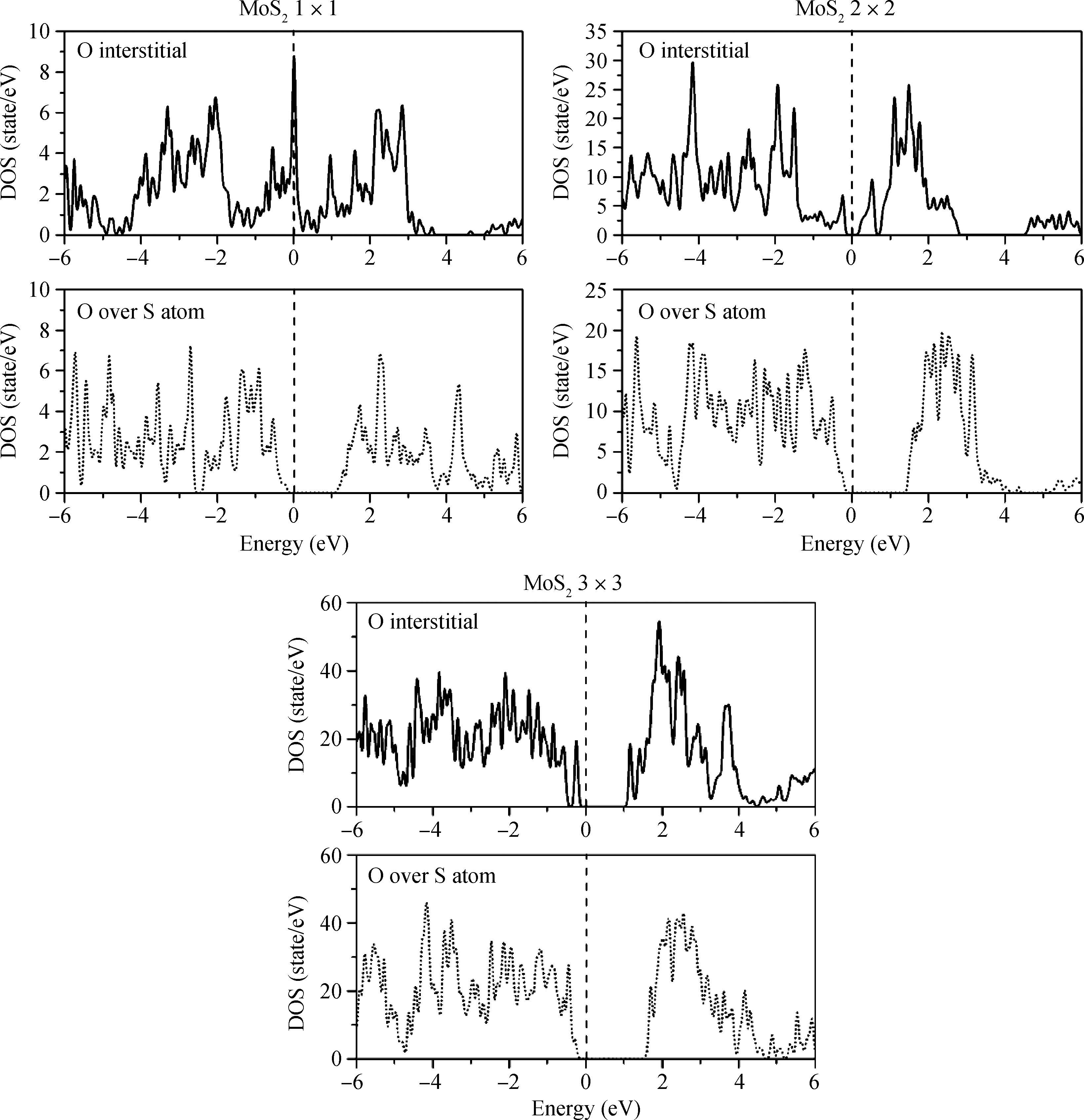
Our theoretical findings demonstrate for the first time a possibility of band-gap engineering of monolayer MoS2 crystals by oxygen and the presence of vacancies. Oxygen atoms are revealed to substitute sulfur ones, forming stable MoS2-xOx ternary compounds, or adsorb on top of the sulfur atoms. The substituting oxygen provides a decrease of the band gap from 1.86 to 1.64 eV and transforms the material from a direct-gap to an indirect-gap semiconductor. The surface adsorbed oxygen atoms decrease the band gap up to 0.98 eV depending on their location tending to the metallic character of the electron energy bands at a high concentration of the adsorbed atoms. Oxygen plasma processing is proposed as an effective technology for such band-gap modifications.

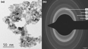
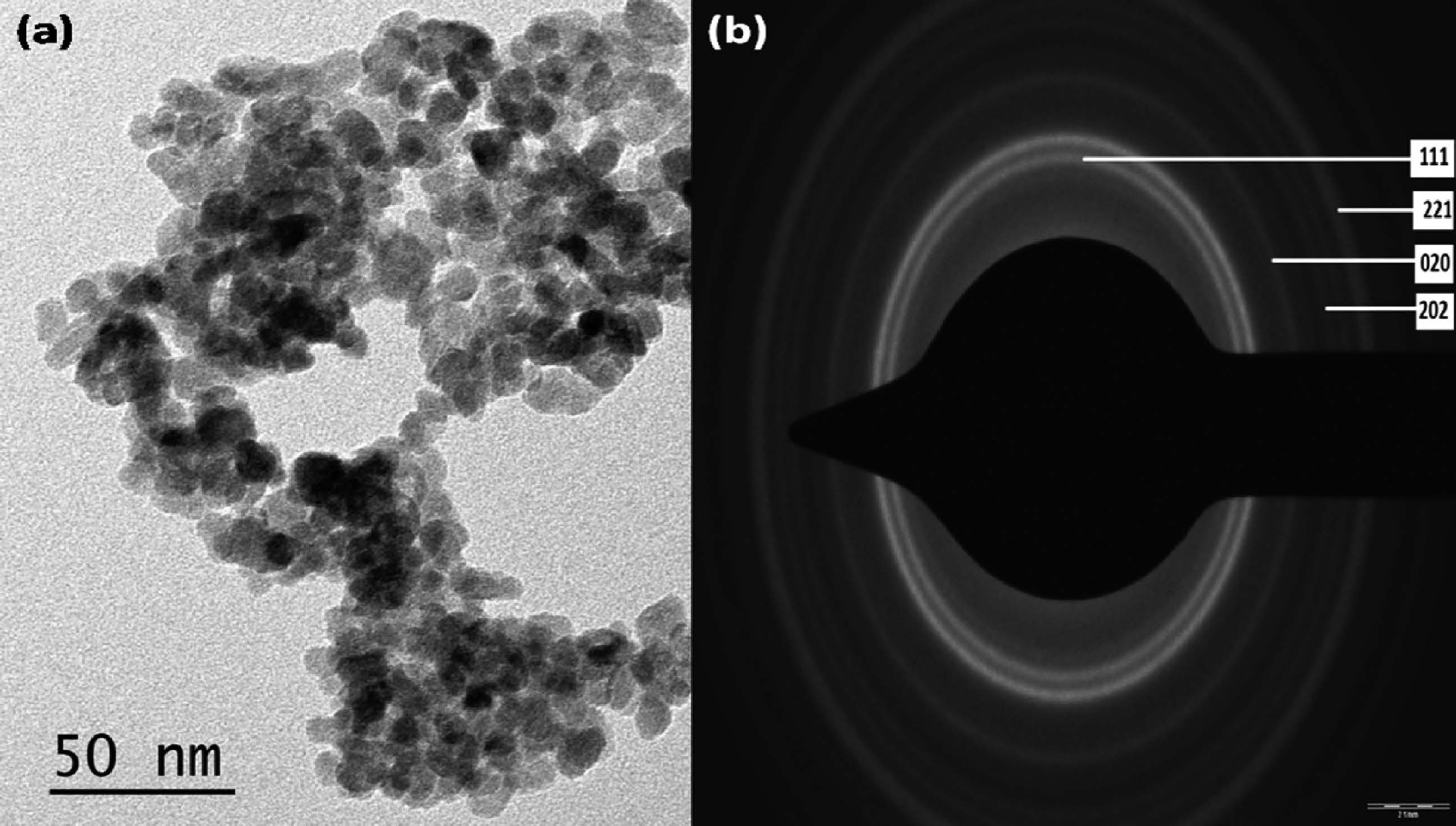
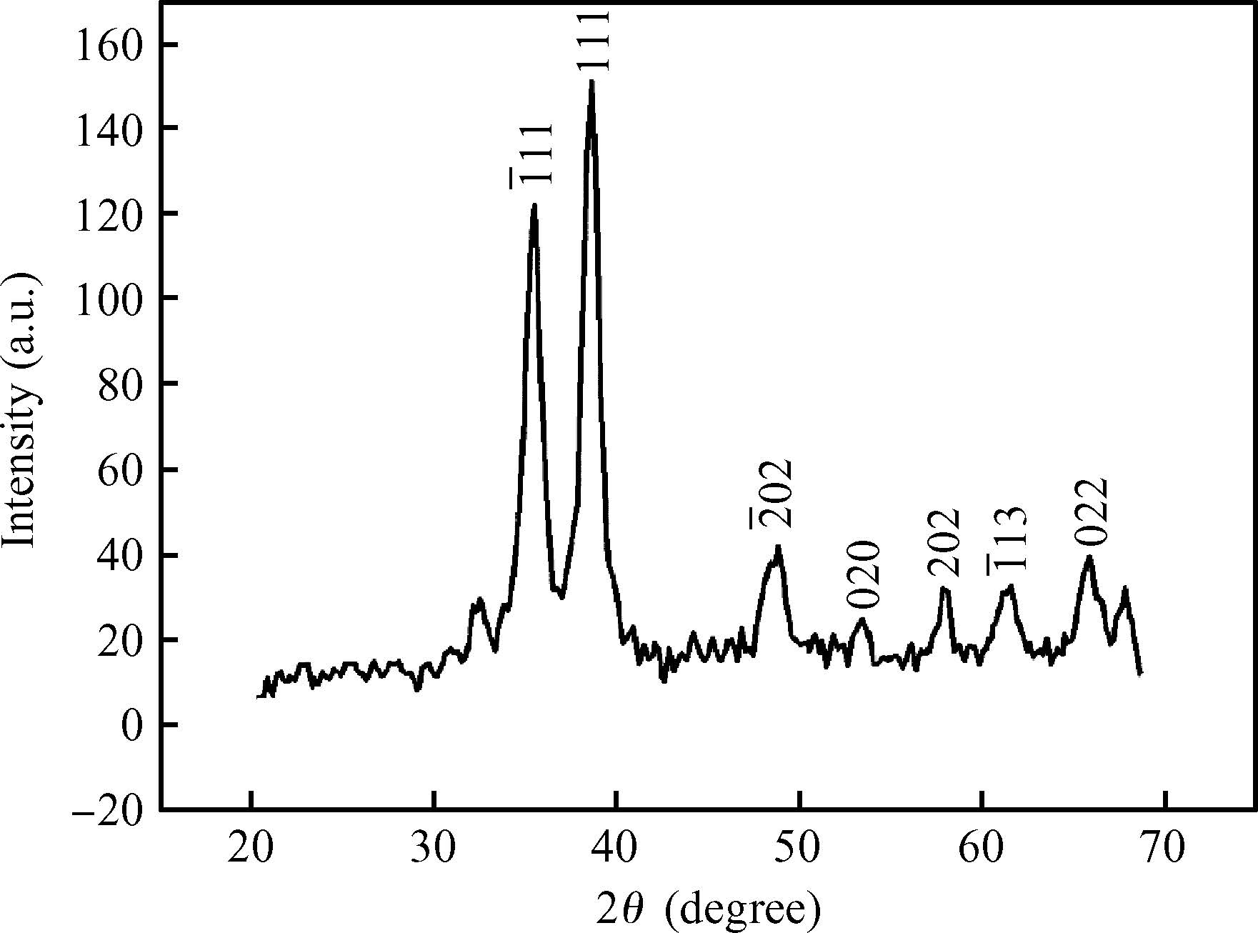
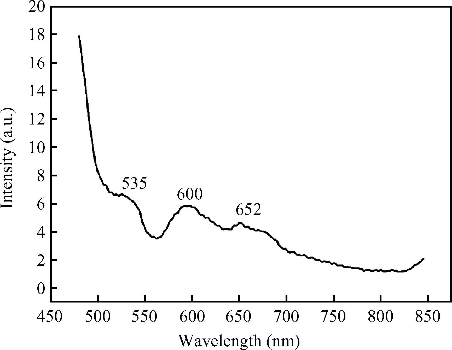
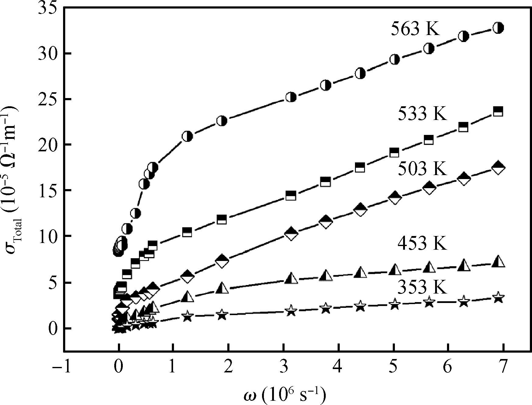
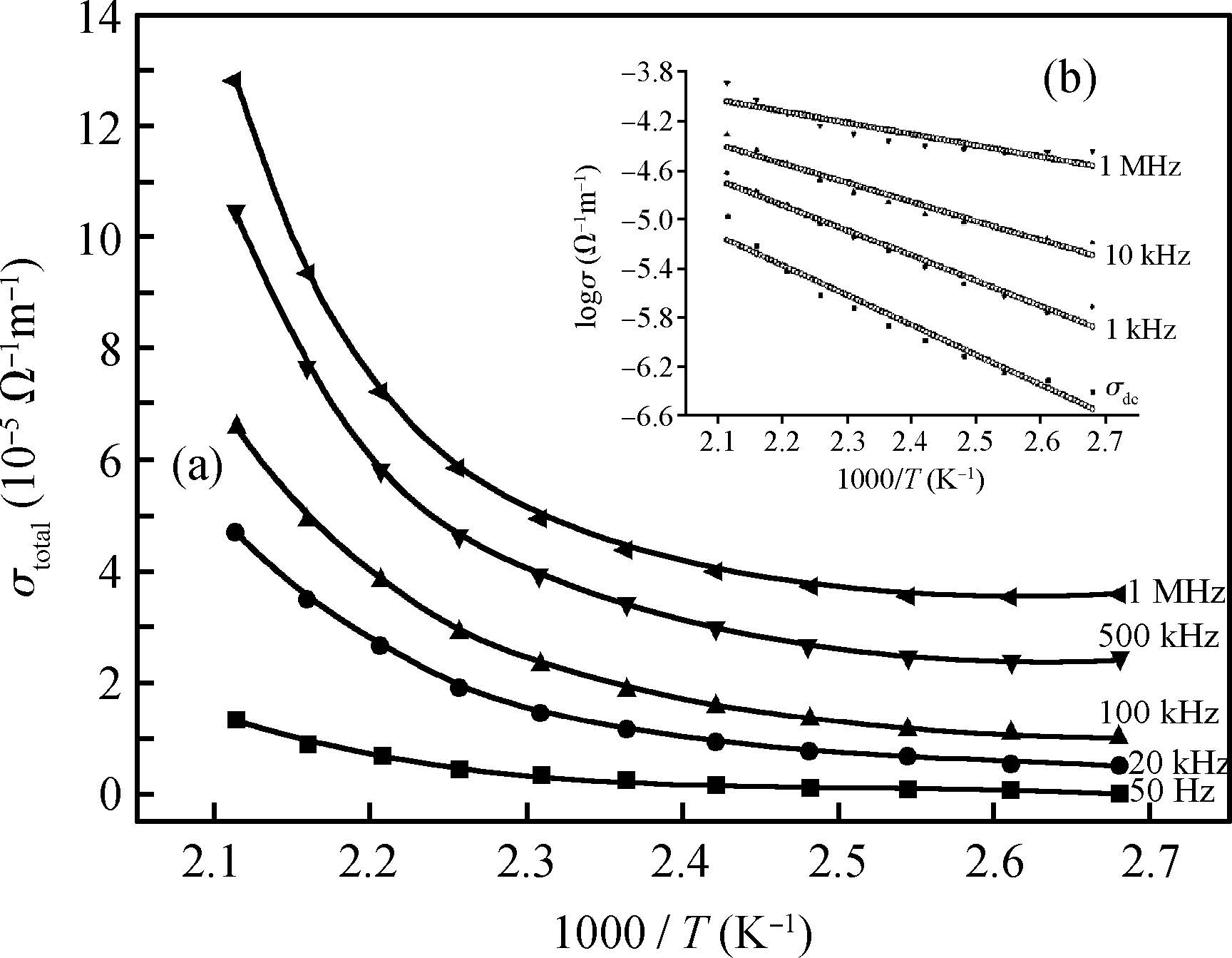
The ac conduction mechanism in copper oxide nanoparticles with 8 nm size, synthesized by a precipitation method was studied by analyzing ac conductivity in the frequency range of 50 Hz-1 MHz and in the temperature range of 373-573 K. X-ray diffraction and transmission electron microscopy(TEM) were employed for the structural and morphological characterization of CuO nanoparticles. The experimental and theoretical investigations suggested that the ac conduction mechanism in CuO nanoparticles can be successfully explained by a correlated barrier hopping model, which provided reasonable values for the maximum barrier height and characteristic relaxation time. It was also found that bipolaron hopping become prominent up to a particular temperature and beyond that single polaron hopping predominates. Physical parameters such as hopping distance and density of defect states were also calculated. Photoluminescence studies confirm the presence of a surface defect in CuO nanoparticles.


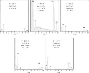
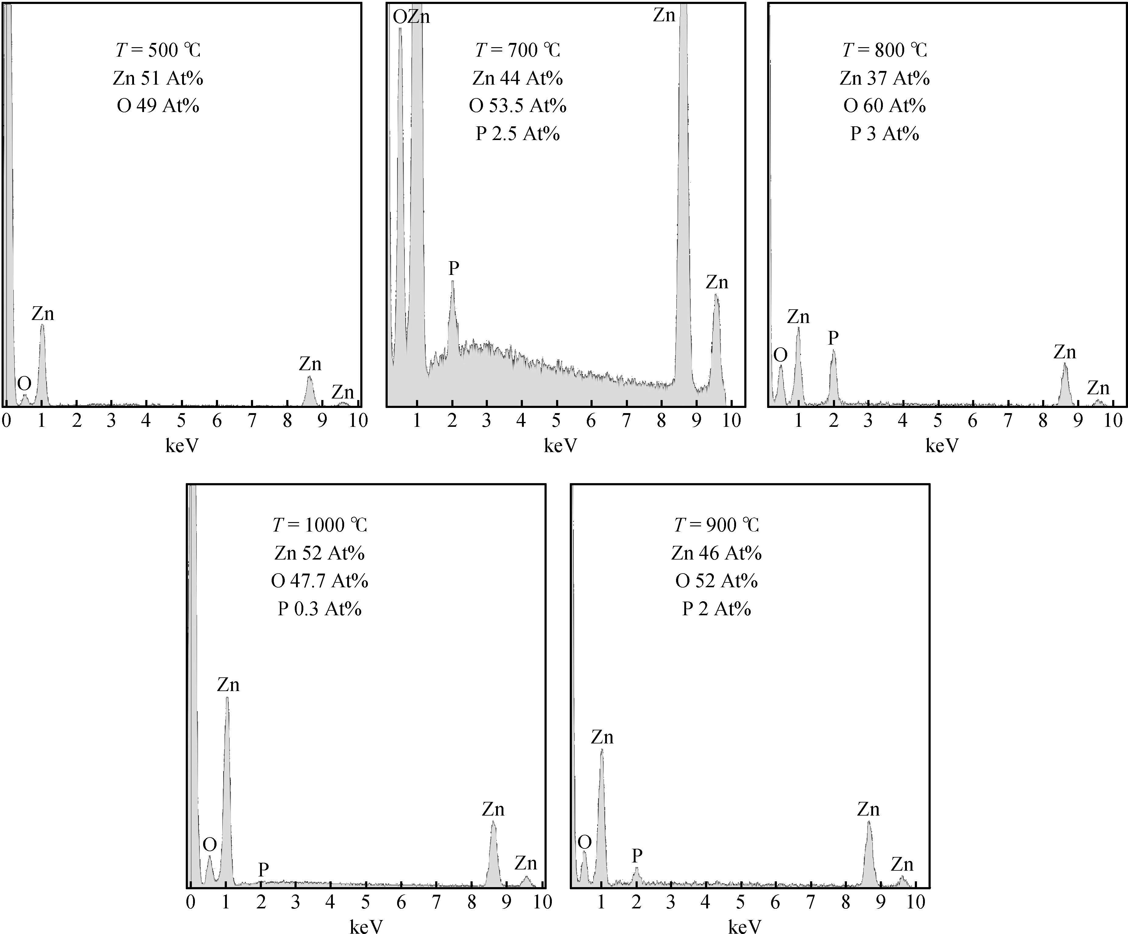
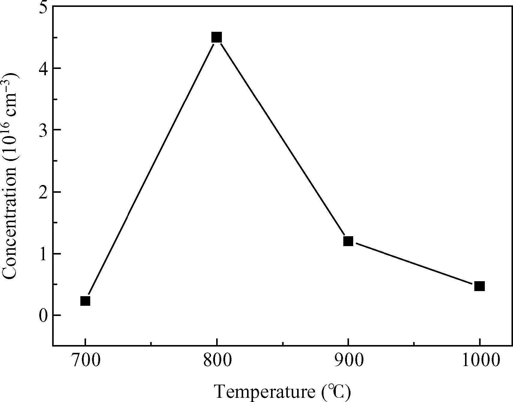
We have demonstrated the effect of annealing temperature on the diffusion density of phosphors in zinc oxide. The P-dopant P430 was sprayed on ZnO pellets and annealed at different temperatures from 500 to 1000℃ with a step of 100℃ for one hour using a programmable furnace. The concentration of P was controlled by varying the annealing temperature and the maximum solubility of P(3% At) was achieved at annealing 800℃ determined by energy dispersive X-ray diffraction(EDX) measurements. X-ray diffraction(XRD) confirmed the hexagonal structure of ZnO and showed that the growth direction was along the c-axis. We observed a maximum up shift in the(002) plane at an annealing temperature of 800℃, suggesting that P atoms replaced Zn atoms in the structure which results in the reduction of the lattice constant. Room temperature photoluminescence(PL) spectrum consists of a peak at 3.28 eV and related to band edge emission, but samples annealed at 800 and 900℃ have an additional donor acceptor pair peak at 3.2 eV. Hall effect measurements confirmed the p-type conductivity of the sample annealed at 800℃.


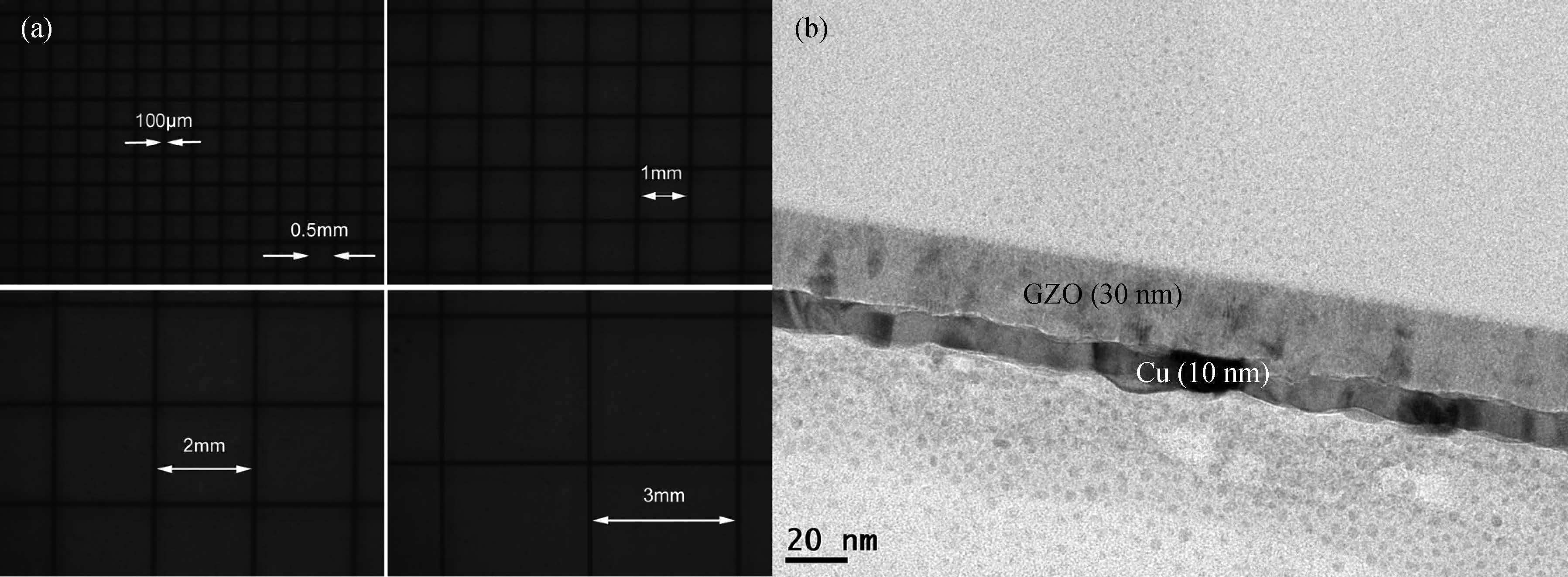
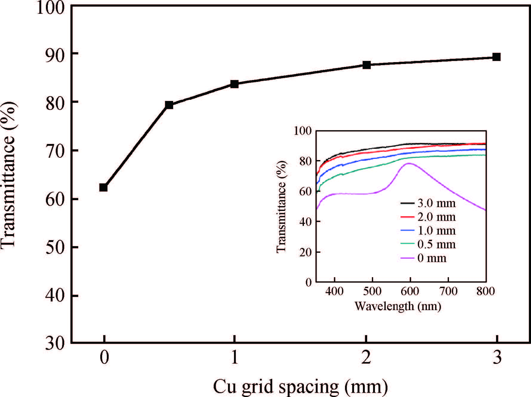
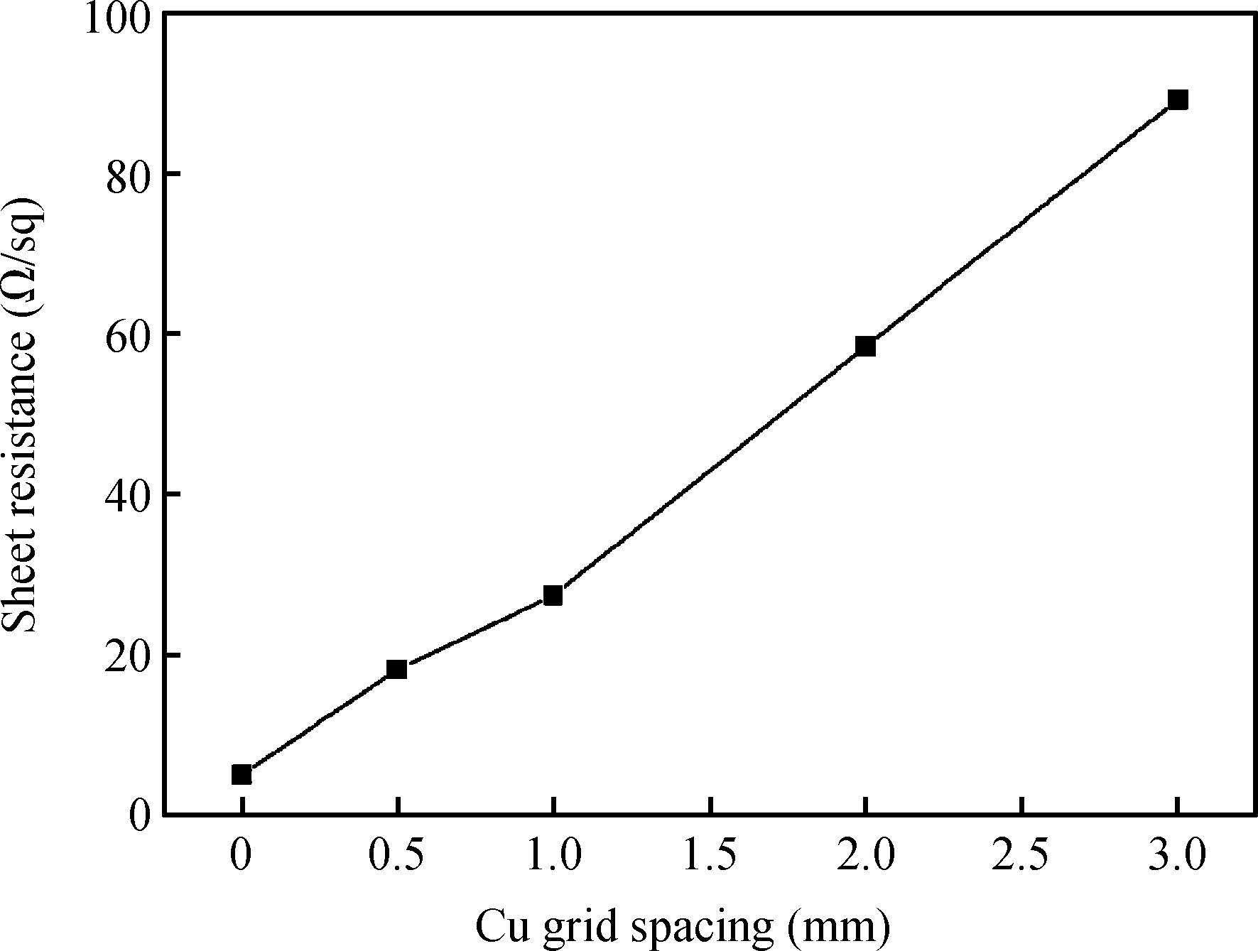
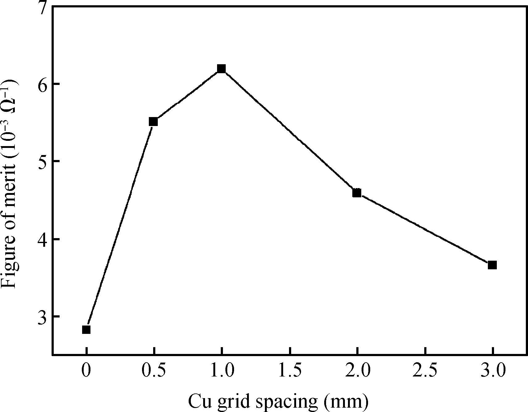
Ga doped ZnO(GZO)/Cu grid double layer structures were prepared at room temperature(RT). We have studied the electrical and optical characteristics of the GZO/Cu grid double layer as a function of the Cu grid spacing distance. The optical transmittance and sheet resistance of the GZO/Cu grid double layer are higher than that of the GZO/Cu film double layer regardless of the Cu grid spacing distance and increase as the Cu grid spacing distance increases. The calculated values for the transmittance and sheet resistance of the GZO/Cu grid double layer well follow the trend of the experimentally observed transmittance and sheet resistance ones. For the GZO/Cu grid double layer with a Cu grid spacing distance of 1 mm, the highest figure of merit(ΦTC=6.19×10⁻³ Ω-1) was obtained. In this case, the transmittance, resistivity and filling factor(FF) of the GZO/Cu grid double layer are 83.74%, 1.10×10⁻⁴ Ω·cm and 0.173, respectively.


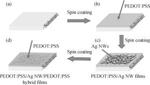
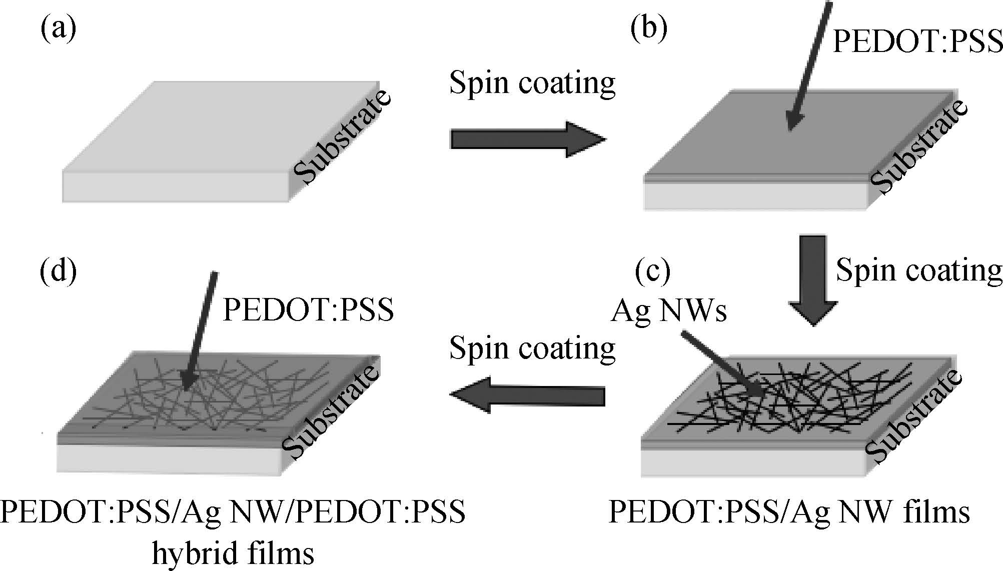
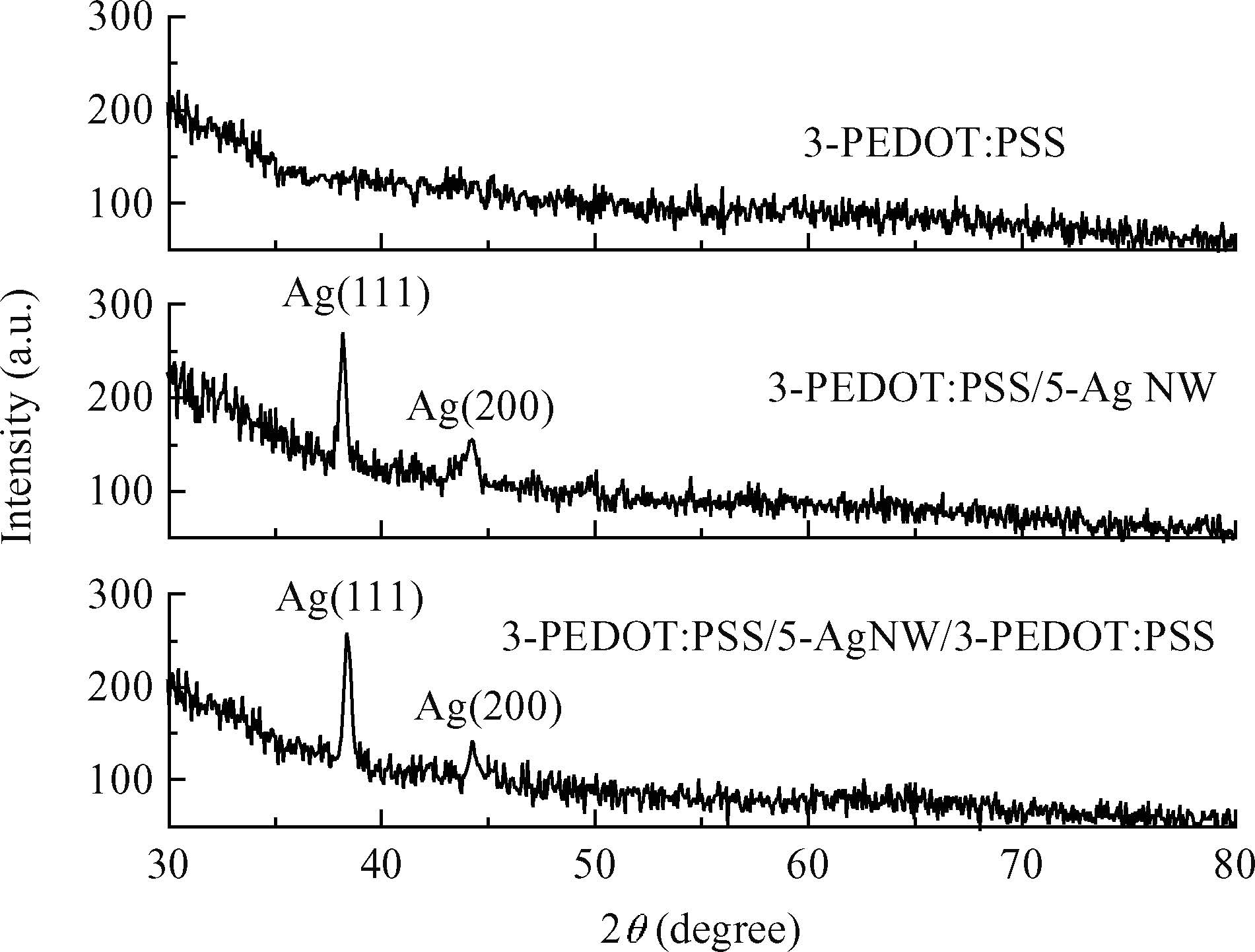
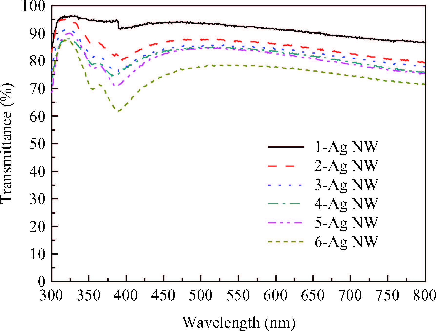
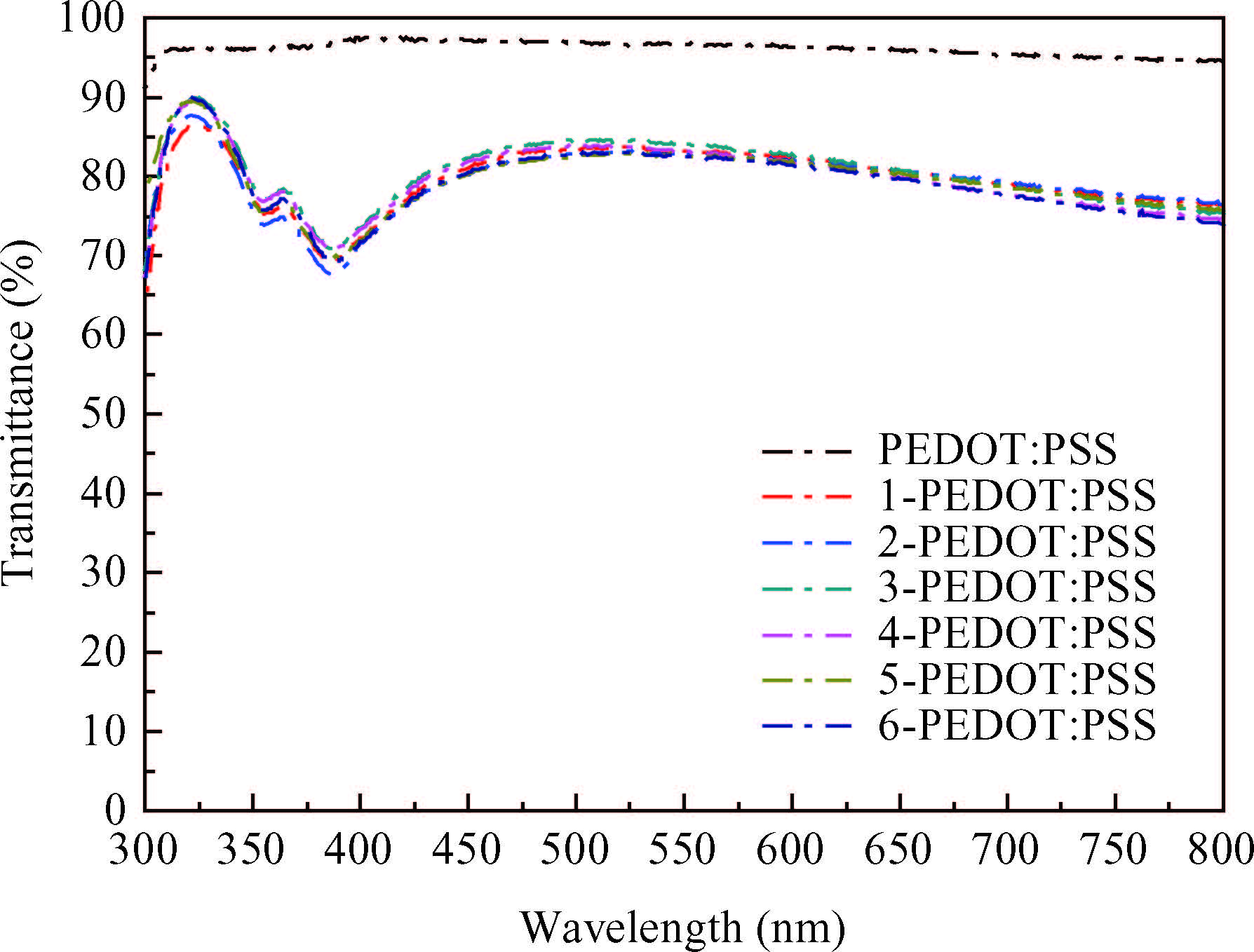
PEDOT:PSS/Ag NW/PEDOT:PSS hybrid films were deposited on PET substrates by the spin coating technique at room temperature. The optical transmittance, sheet resistance, crystallization and surface morphology were characterized by using the double beam spectrophotometer, Hall effect system, X-ray diffractometer and field emission scanning electron microscopy. XRD patterns of the hybrid films display characteristic diffraction peaks of Ag(111) and Ag(200), and the Ag NW networks have a polycrystalline structure with a Ag(111) preferred orientation. A high transmittance of 83.95% at the 550 nm wavelength and a low sheet resistance of 21.98Ω/□ are achieved for 3-PEDOT:PSS/5-Ag NW/3-PEDOT:PSS hybrid films.


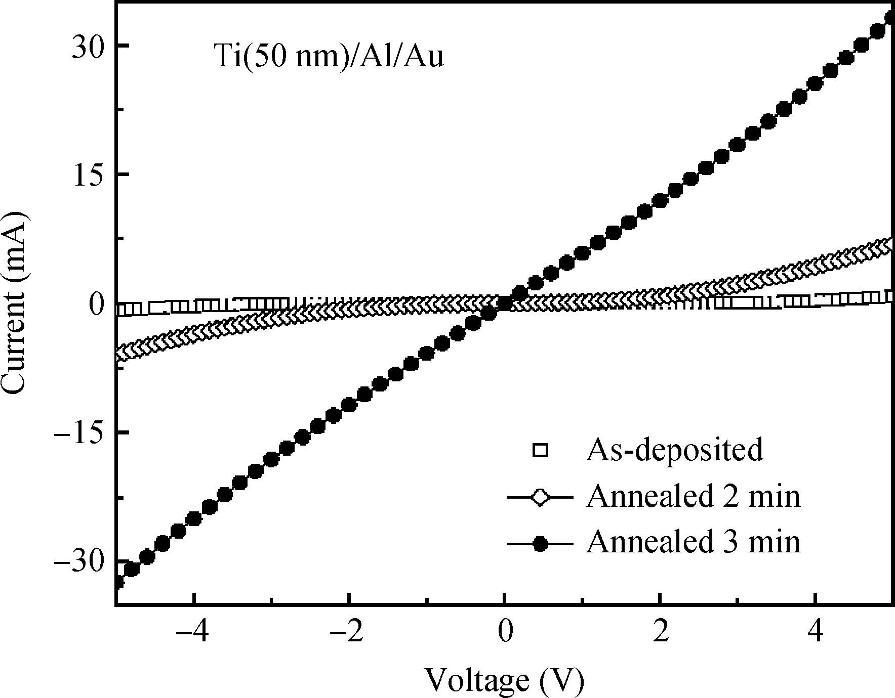
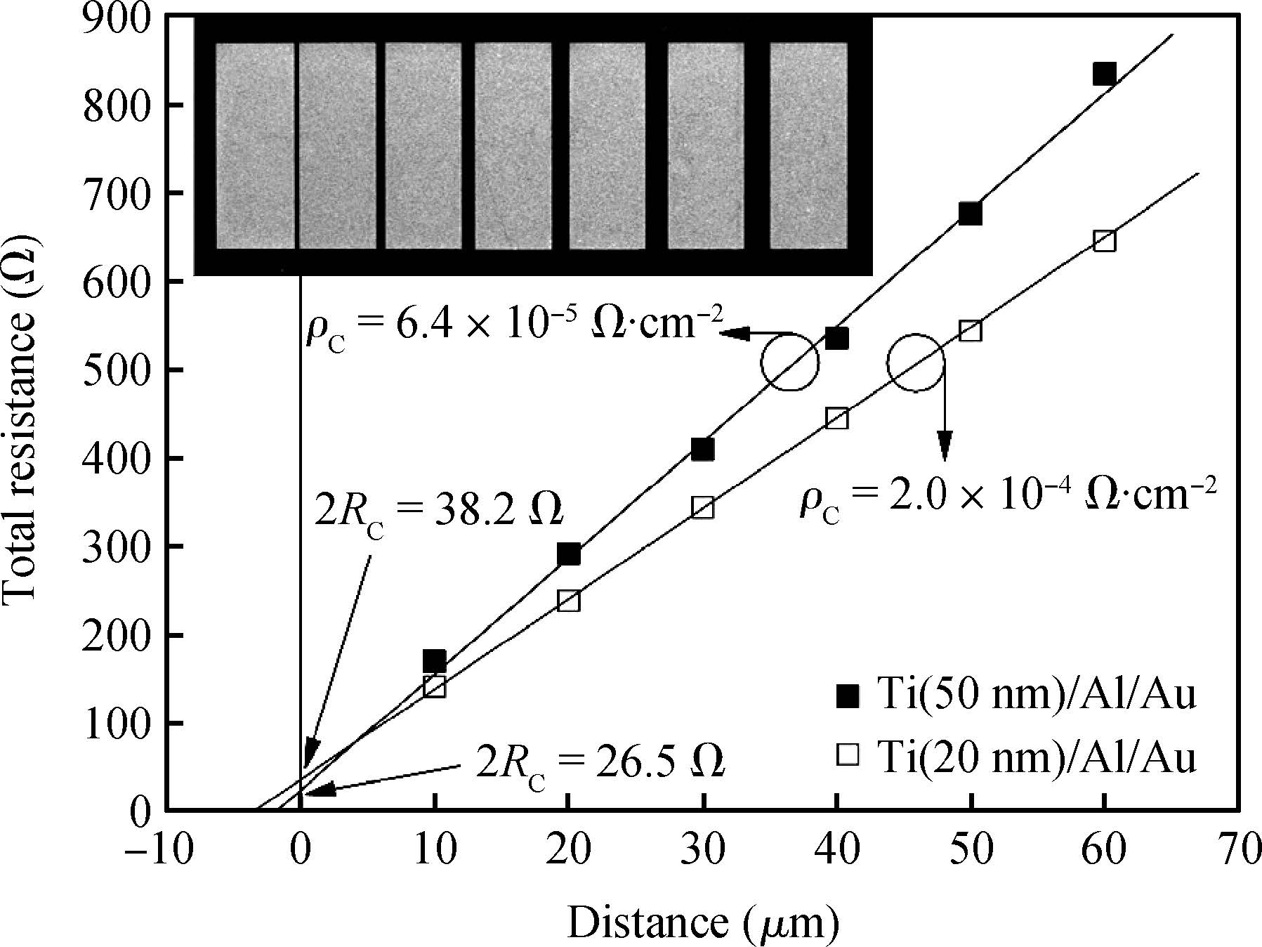
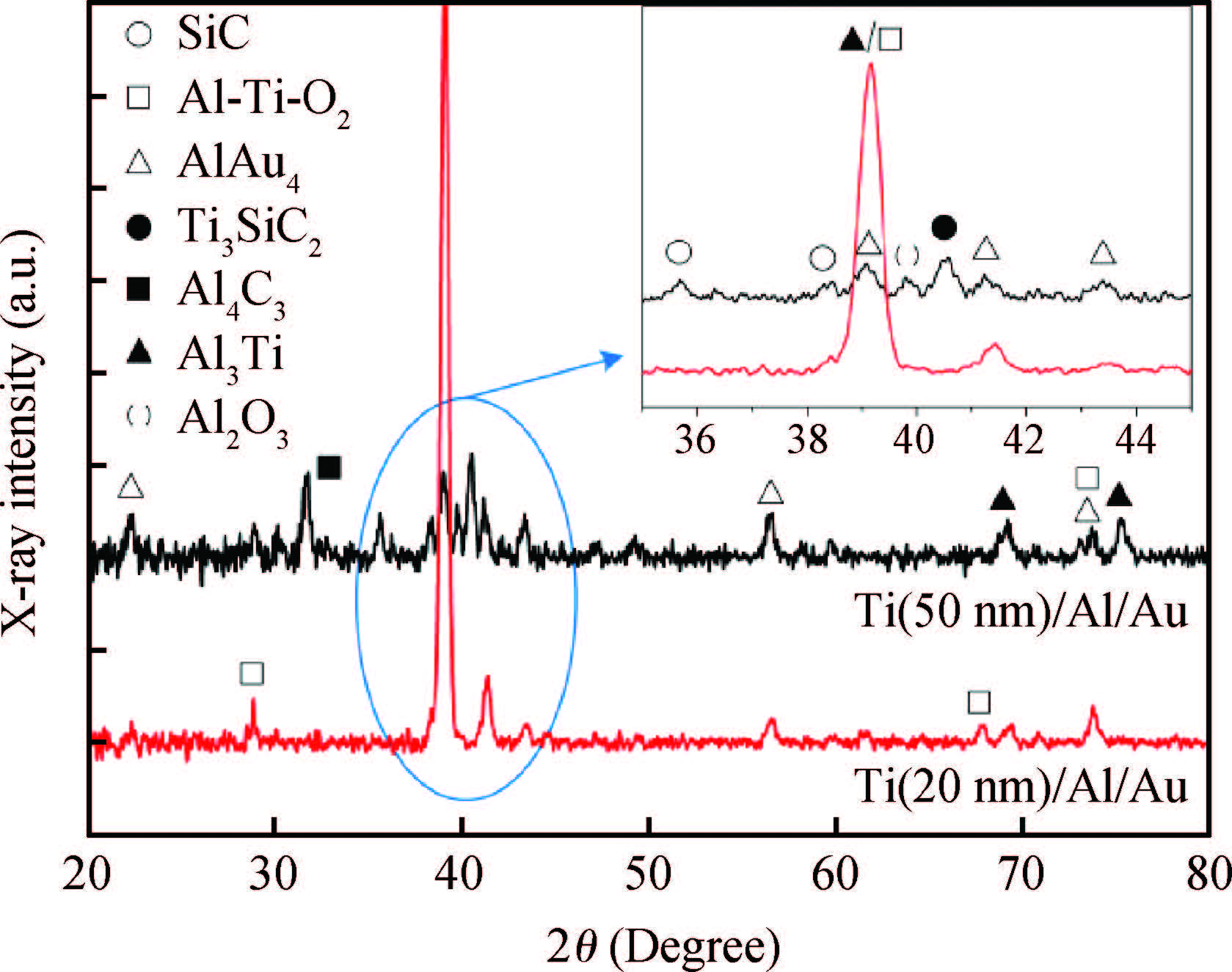
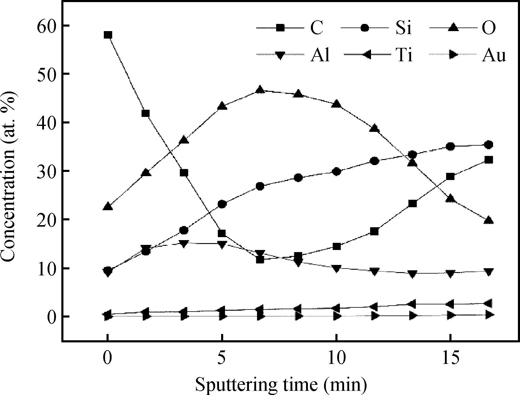
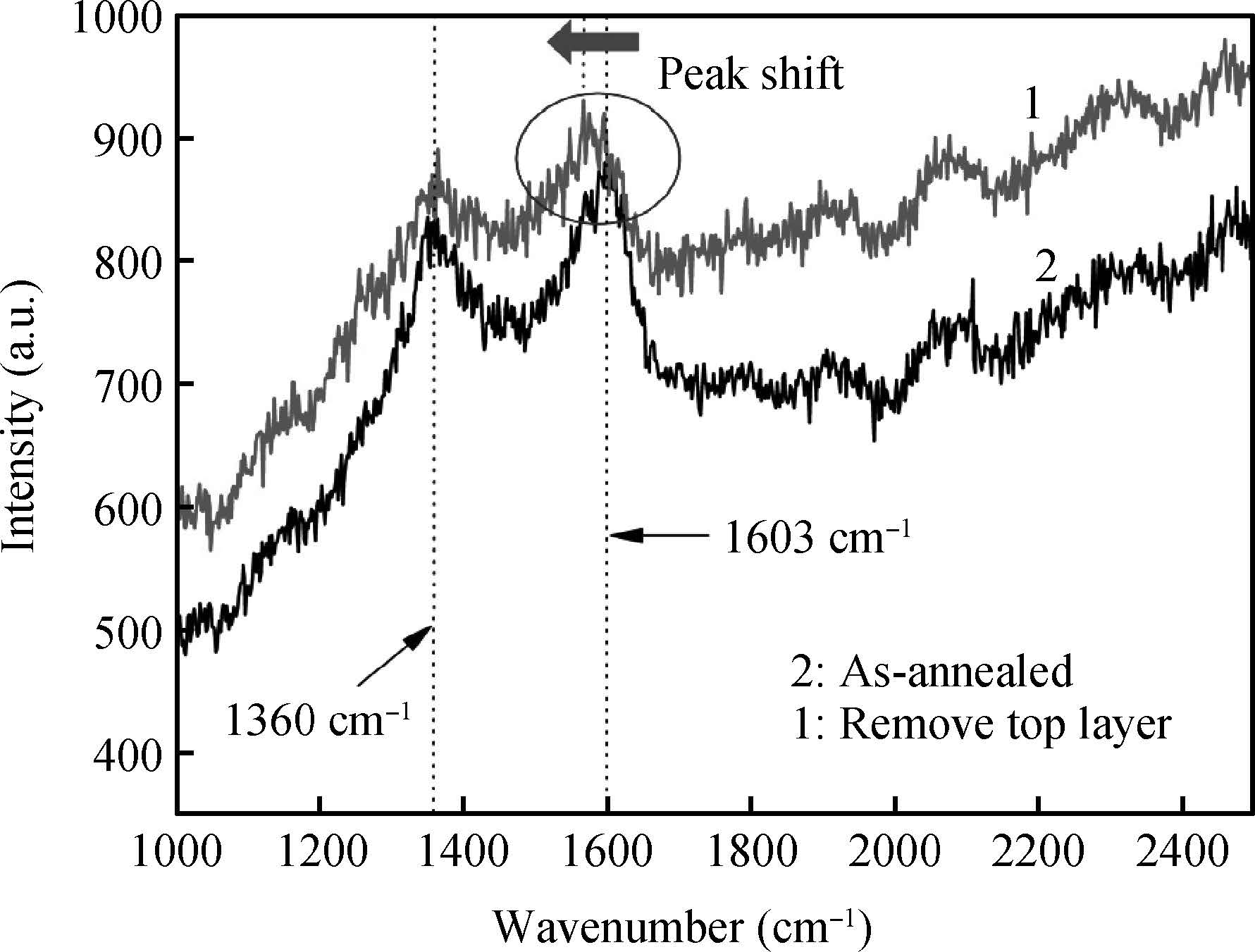
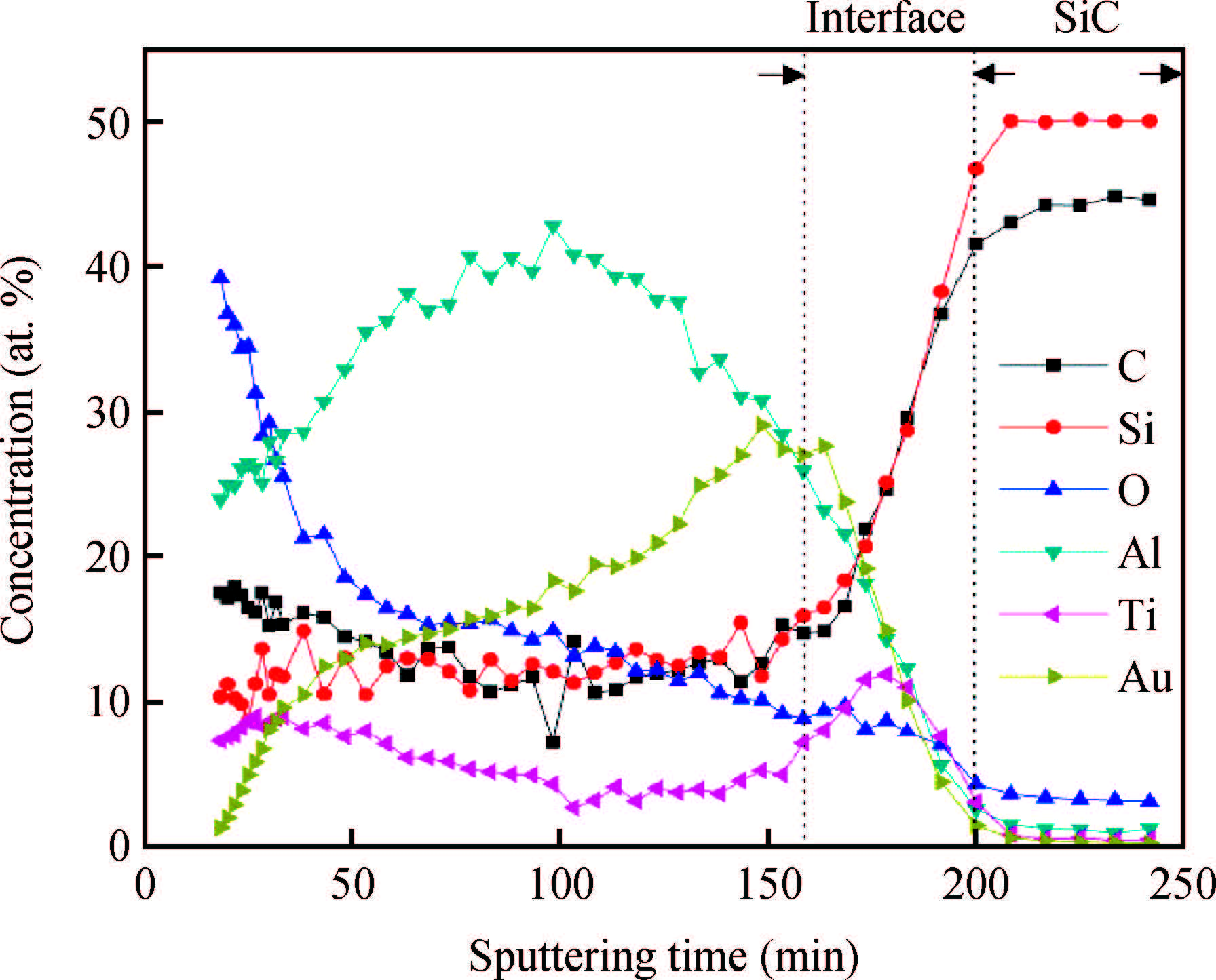
Ti/Al/Au ohmic contacts to p-type 4H-SiC in terms of a different annealing time and Ti composition are reported. At 1050℃, proper increase in annealing time plays a critical role in the Schottky to ohmic contact conversion. With the optimized annealing time, the contact with a high Ti content yields a lower specific contact resistivity(ρc) of 6.4×10⁻⁵ Ω·cm2 compared with the low-Ti contact. The annealed surface morphology and phase resultants were examined by scanning electron microscopy(SEM) and X-ray diffraction(XRD), respectively. For the better ohmic contact, element distribution and chemical states were qualitatively identified by X-ray photoelectron spectroscopy(XPS) depth analysis. In particular, the presence of C and a Si-related phase was discussed and associated with the change in the surface status of the as-grown epilayer of 4H-SiC during annealing. The results reveal that the out-diffused C and Si atoms, with an approximate atomic ratio of 1:1 in the contact layer, can combine to form an amorphous Si-C state. The polycrystalline graphite instead of an unreacted C cluster in the whole alloyed structure and an extra nanosize graphite flake on the outermost surface of the annealed contact were confirmed by Raman spectroscopy.


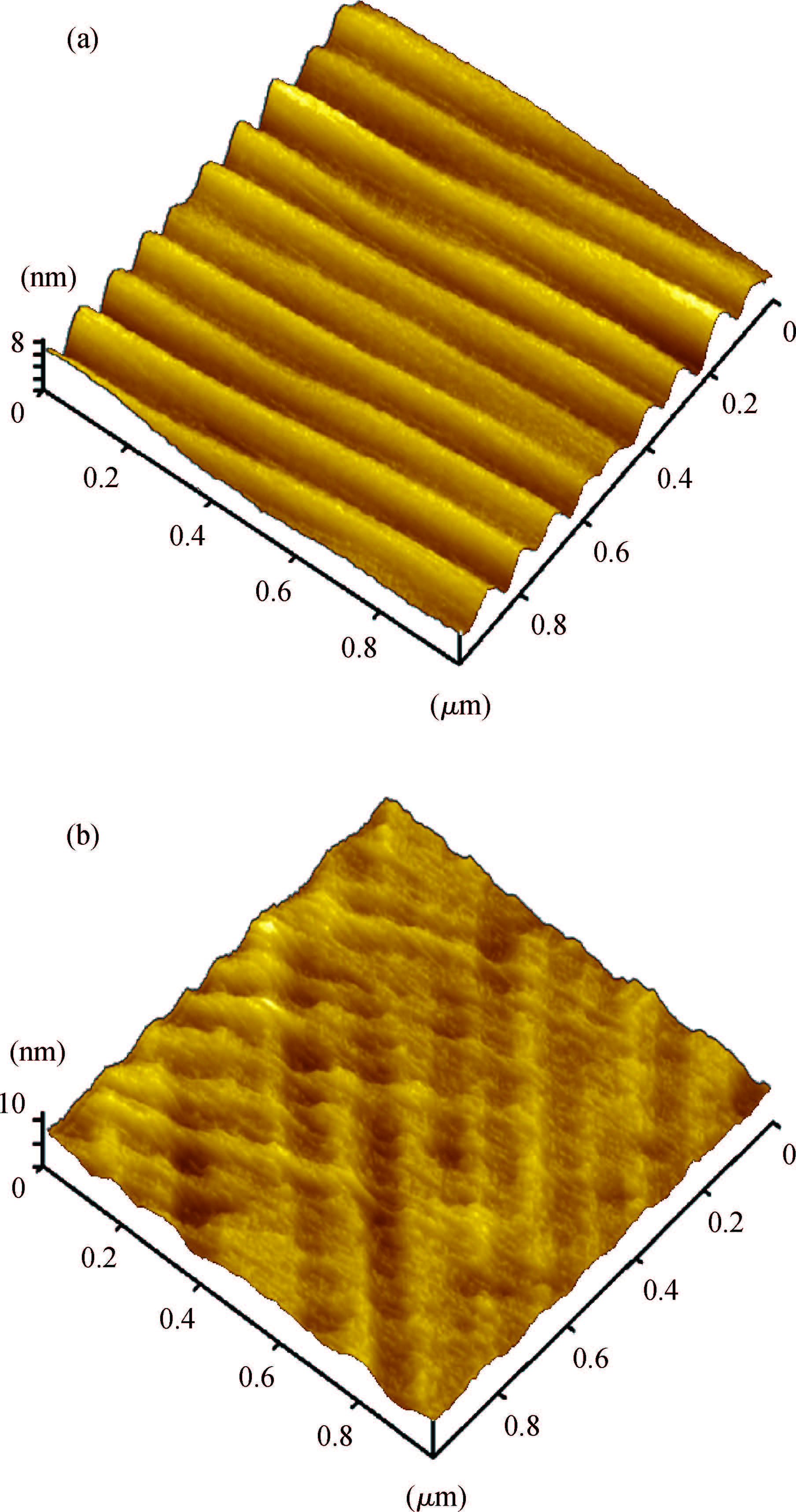
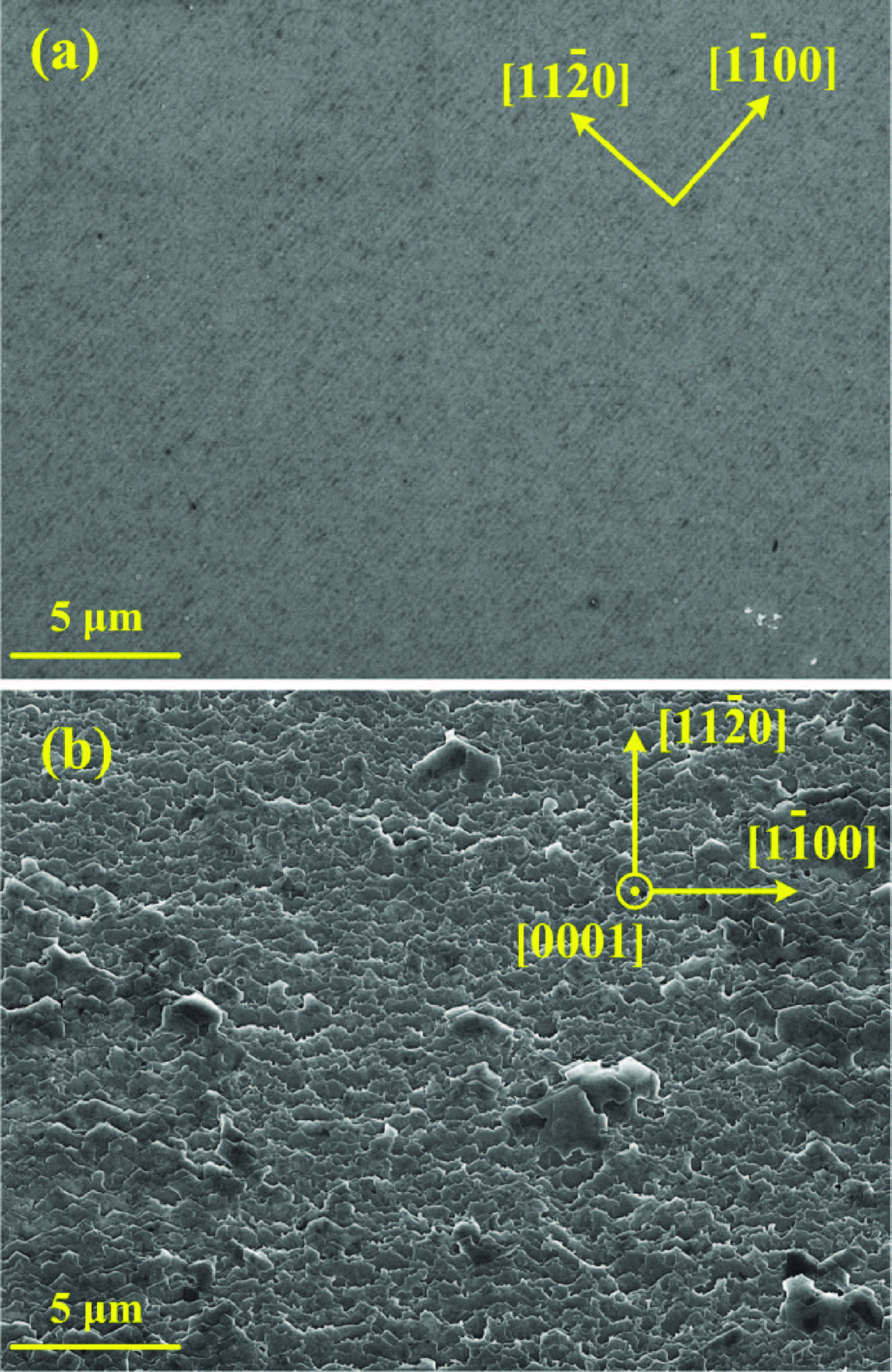
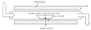
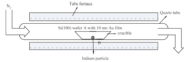
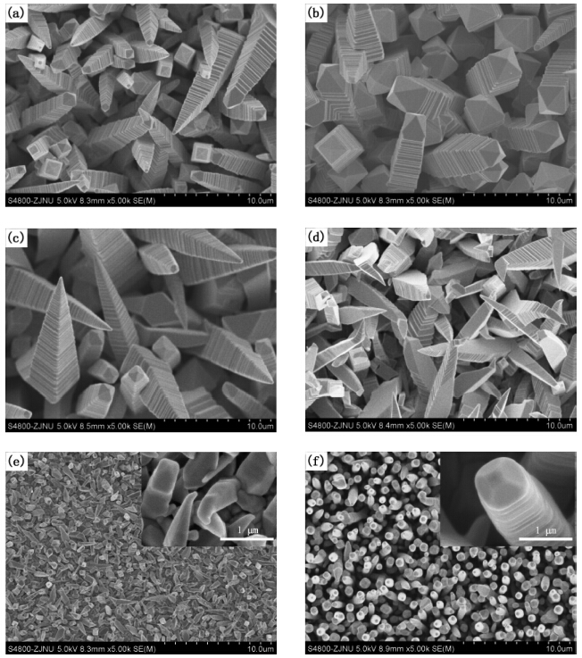
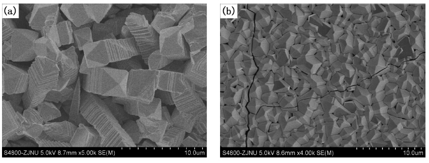
Large-scale In2O3 nanotowers with different cross sections were synthesized by a thermal evaporation and oxidation technique using metal as the catalyst. The morphologies and structural characterizations of In2O3 nanotowers are dependent on growth processes, such as different metal(Au, Ag or Sn) catalysts, the relative position of the substrate and evaporation source, growth temperature, gas flow rate, and growth time. In2O3 nanotowers cannot be observed using Sn as the catalyst, which indicates that metal liquid droplets play an important role in the initial stages of the growth of In2O3 nanotowers. The formation of an In2O3 nanotower is attributed to the competitive growth model between a lateral growth controlled by vapor-solid mechanism and an axial vapor-liquid-solid growth mechanism mediated by metal liquid nanodroplets. The synthesized In2O3 nanostructures with novel tower-shaped morphology may have potential applications in optoelectronic devices and gas sensors.

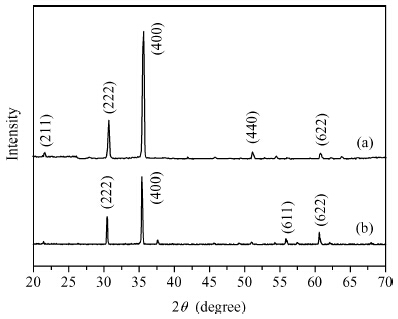


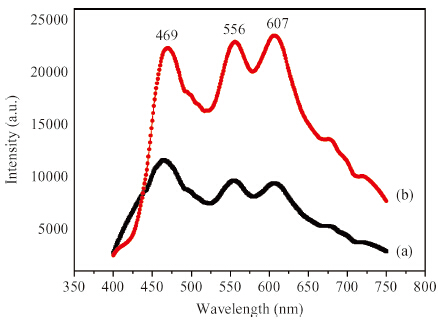

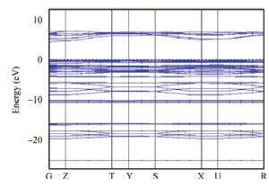
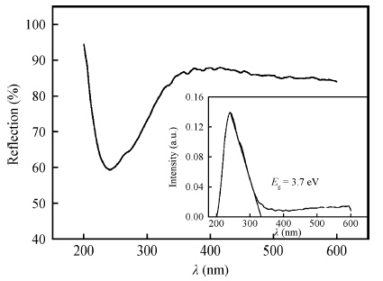
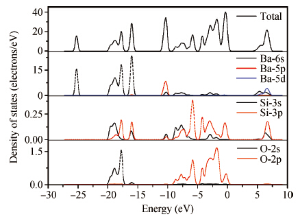
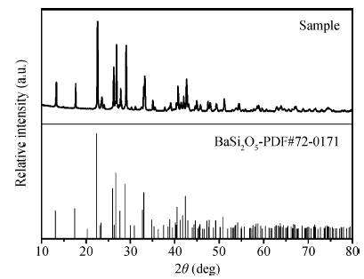
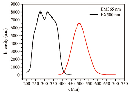
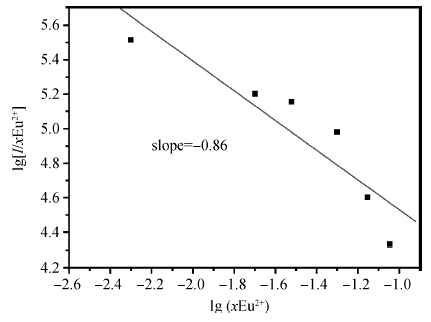
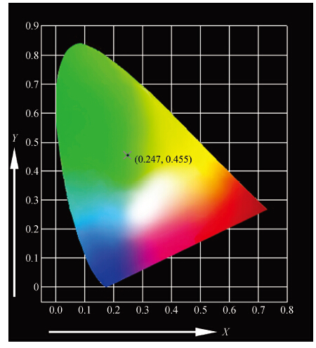
The green-emitting phosphor BaSi2O5:Eu2+ was synthesized by the conventional solid state reaction. Using the CASTEP code, BaSi2O5 is calculated to be an intermediate band gap semiconductor with an indirect energy gap of about 3. 2 eV. As expected, the calculated optical band gap of BaSi2O5 is lower compared to the experimentally determined values. Eu2+-activated BaSi2O5 phosphor can be excited efficiently over a broad spectral range between 200 and 400 nm, and has an emission peak at 500 nm with a full width at half maximum of 95 nm. The study of concentration-dependent emission intensity shows the optimal concentration of the Eu2+ is 0.05 mol, and that concentration quenching occurs when the Eu2+ content is beyond the critical value. The external quantum efficiency of the optimized BaSi2O5:Eu2+ is 96. 1%, 70. 2% and 62. 1% under excitation at 315, 350 and 365 nm, respectively. The superior optical properties of the sample show the potential as an ultraviolet converting green-emitting phosphor for white light emitting diodes.


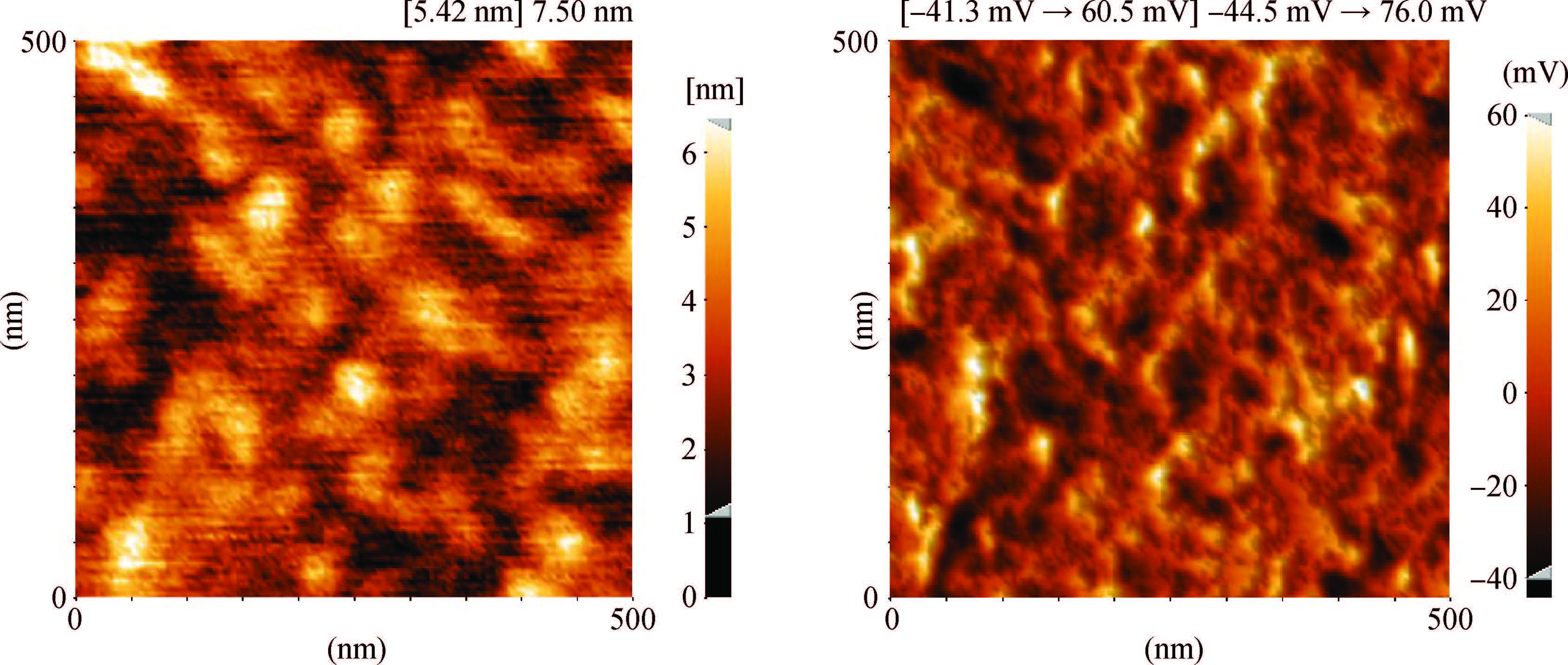
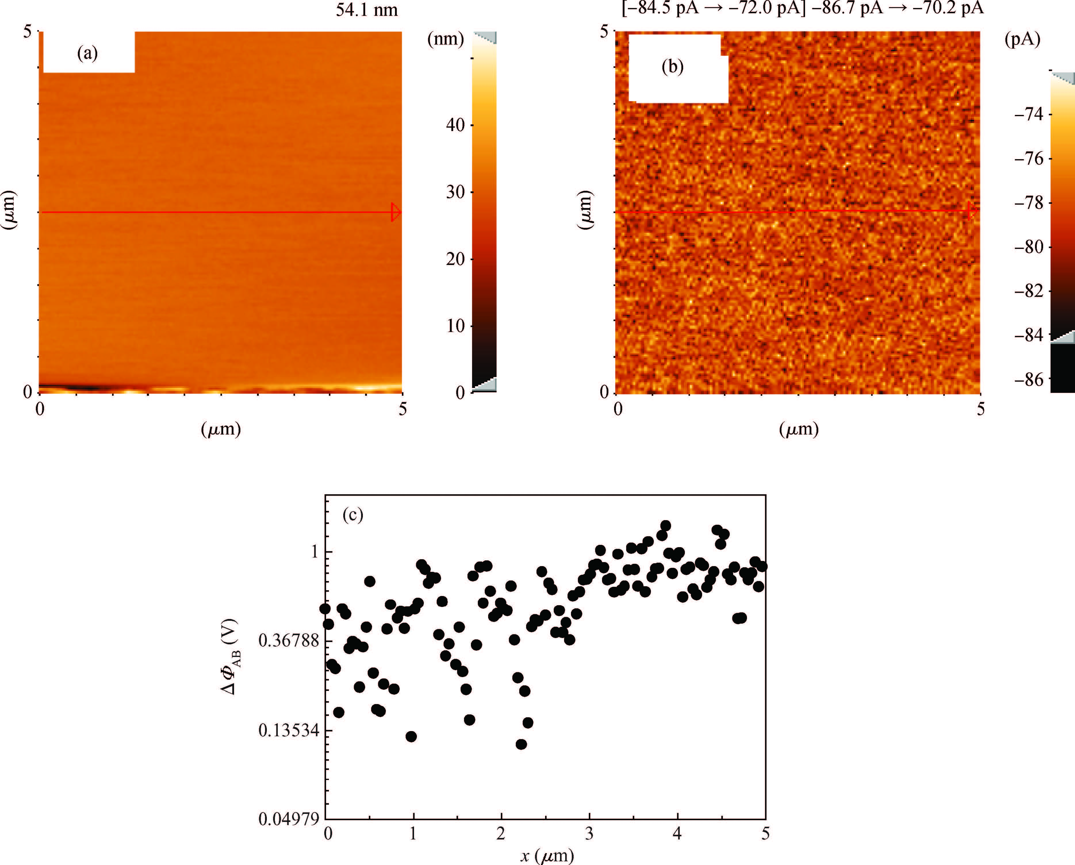
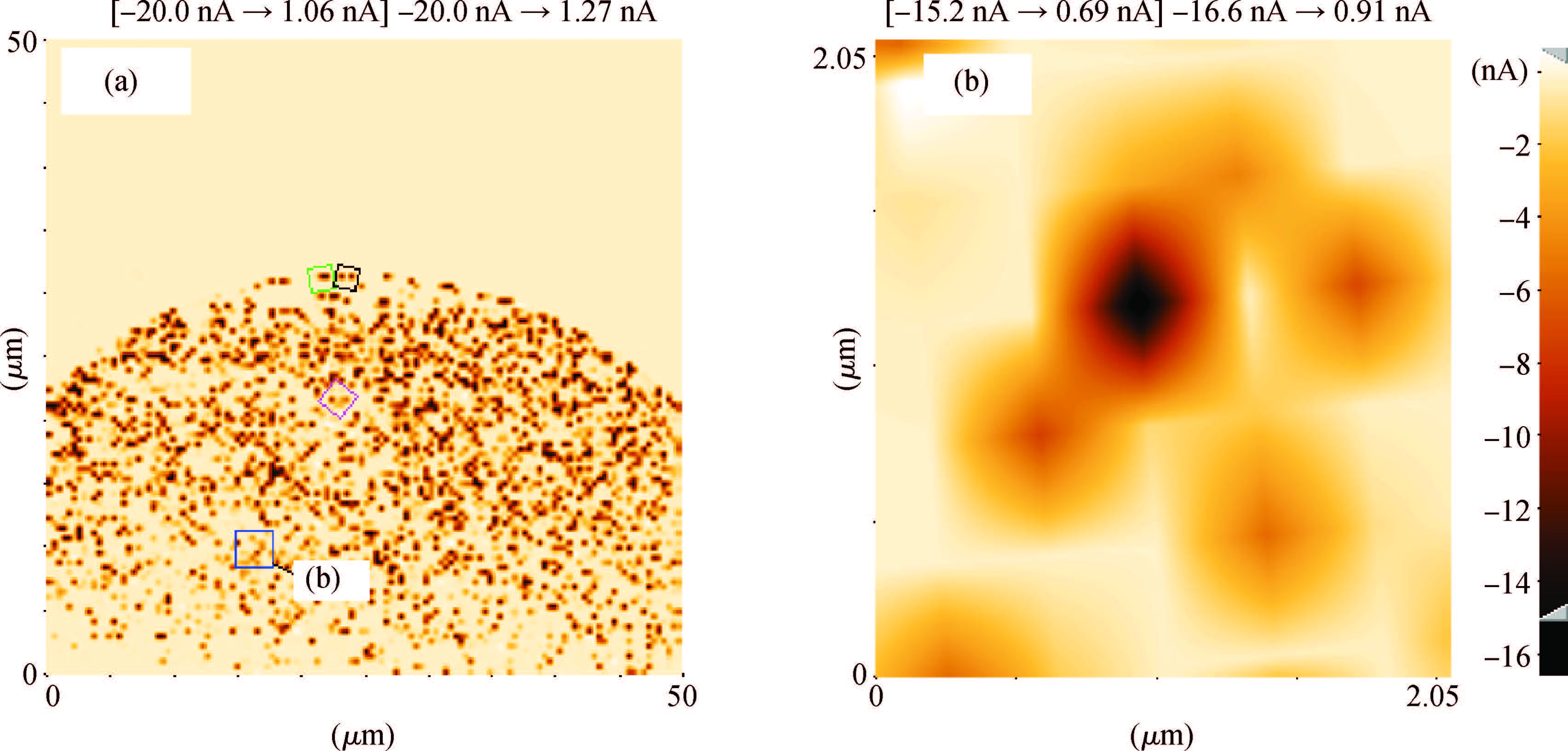
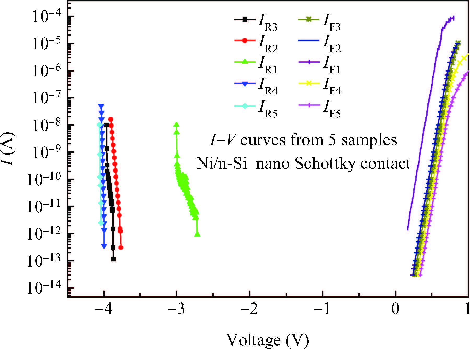
We have experimentally studied the Ni/n-Si nano Schottky barrier height(SBH) and potential difference between patches in the nano Schottky diodes(SD) using contact atomic force microscopy(C-AFM) in tapping mode and scanning tunneling microscopy(STM). Topology measurement of the surface with C-AFM showed that, a single Ni/n-Si SD consists of many patches with different sizes. These patches are sets of parallel diodes and electrically interacting contacts of 5 to 50 nm sizes and between these individual diodes, there exists an additional electric field. In real metal semiconductor contacts(MSC), patches with quite different configurations, various geometrical sizes and local work functions were randomly distributed on the surface of the metal. The direction and intensity of the additional electric field are distributed in homogenously along the contact metal surface. SBH controls the electronic transport across the MS interface and therefore, is of vital importance to the successful operation of semiconductor devices.


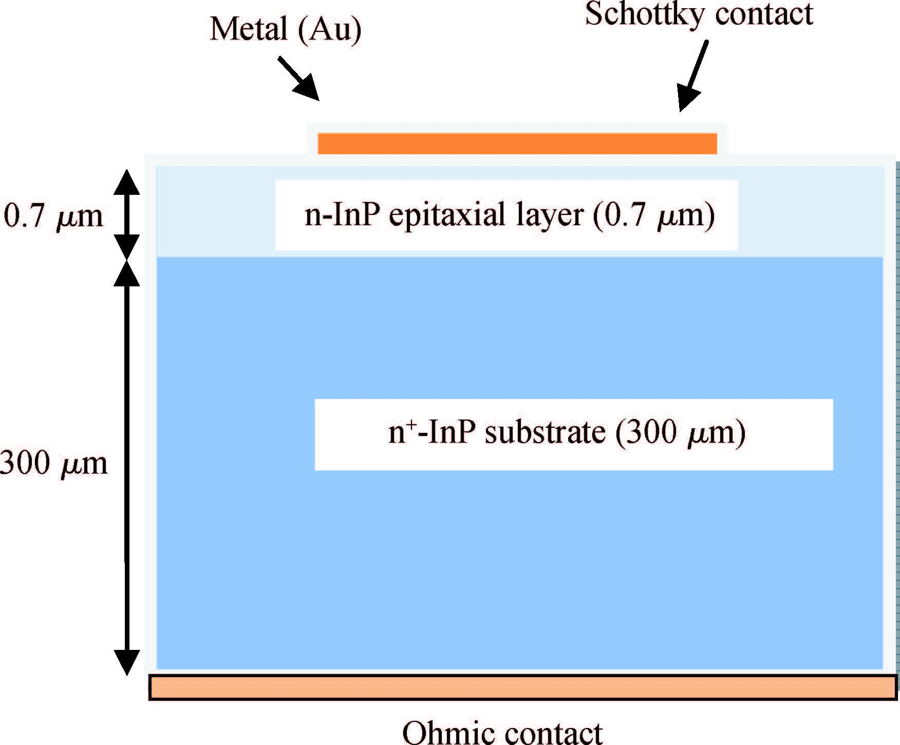
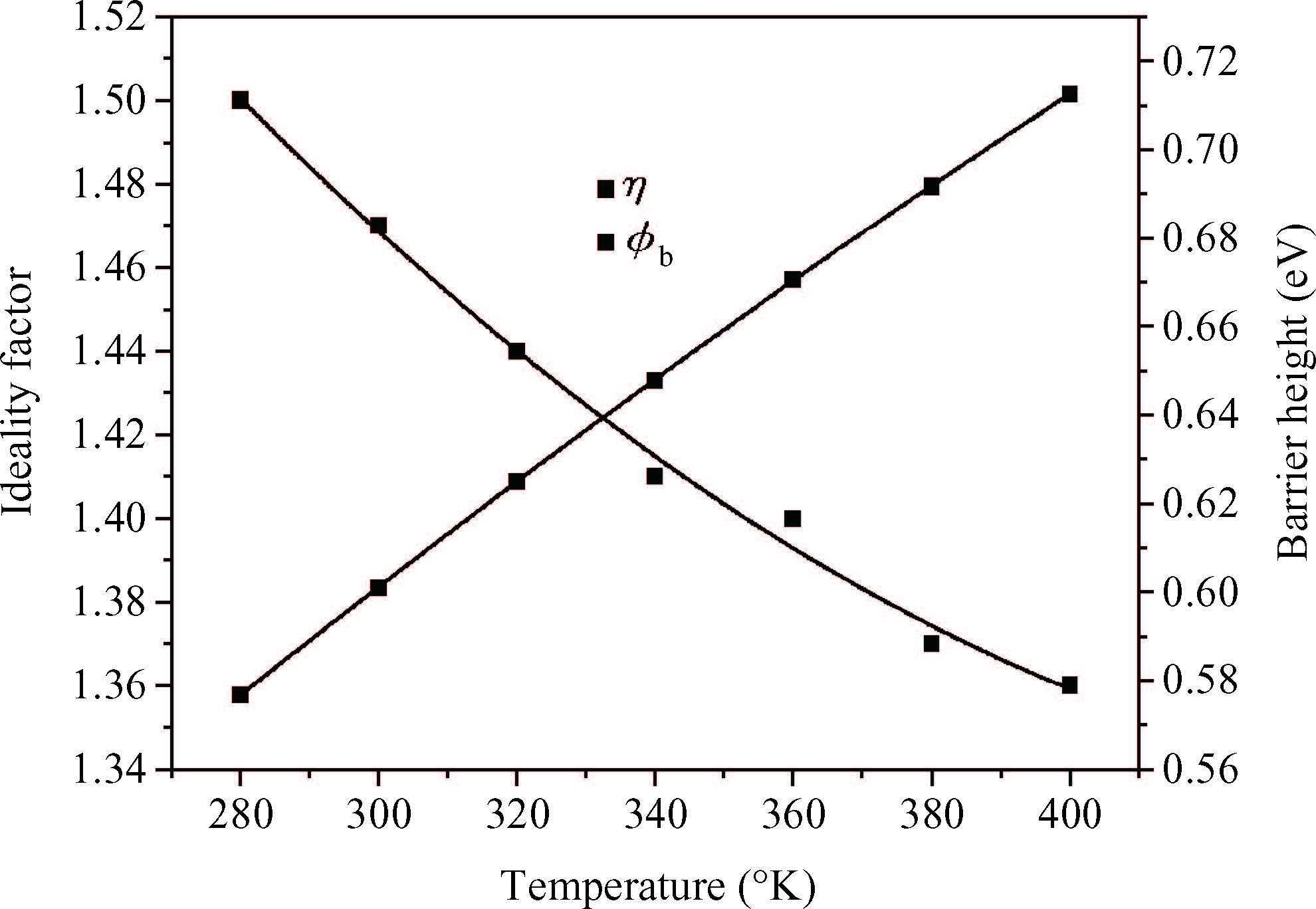
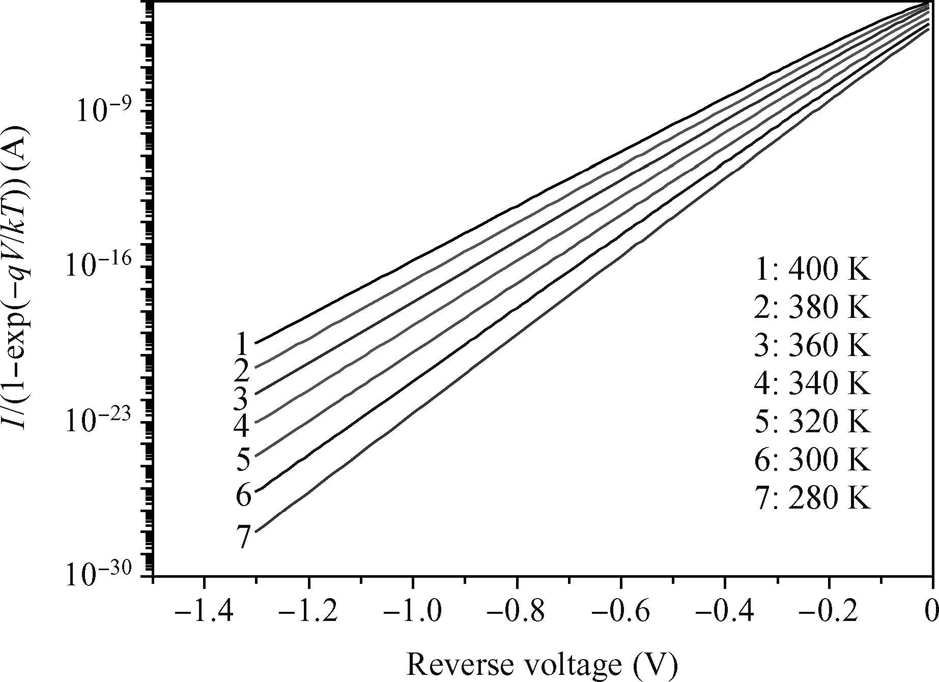
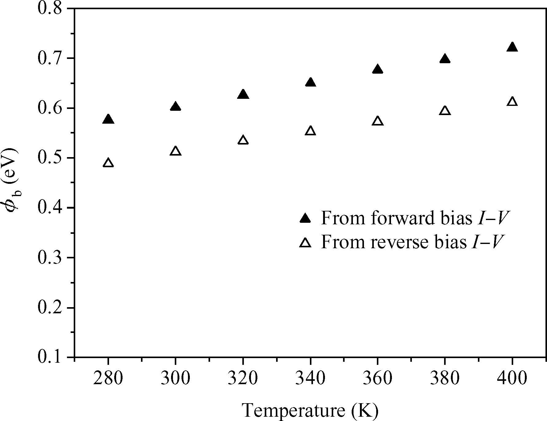
We report the current-voltage(I-V) characteristics of the Schottky diode(Au/n-InP) as a function of temperature. The SILVACO-TCAD numerical simulator is used to calculate the I-V characteristic in the temperature range of 280-400 K. This is to study the effect of temperature on the I-V curves and assess the main parameters that characterize the Schottky diode such as the ideality factor, the height of the barrier and the series resistance. The I-V characteristics are analyzed on the basis of standard thermionic emission(TE) theory and the inhomogeneous barrier heights(BHs) assuming a Gaussian distribution. It is shown that the ideality factor decreases while the barrier height increases with increasing temperature, on the basis of TE theory. Furthermore, the homogeneous BH value of approximately 0.524 eV for the device has been obtained from the linear relationship between the temperature-dependent experimentally effective BHs and ideality factors. The modified Richardson plot, according to the inhomogeneity of the BHs, has a good linearity over the temperature range. The evaluated Richardson constant A* was 10.32 A·cm-2·K-2, which is close to the theoretical value of 9.4 A·cm-2·K-2 for n-InP. The temperature dependence of the I-V characteristics of the Au/n-InP Schottky diode have been successfully explained on the basis of the thermionic emission(TE) mechanism with a Gaussian distribution of the Schottky barrier heights(SBHs). Simulated I-V characteristics are in good agreement with the measurements[Korucu D, Mammadov T S. J Optoelectronics Advanced Materials, 2012, 14:41]. The barrier height obtained using Gaussian Schottky barrier distribution is 0.52 eV, which is about half the band gap of InP.

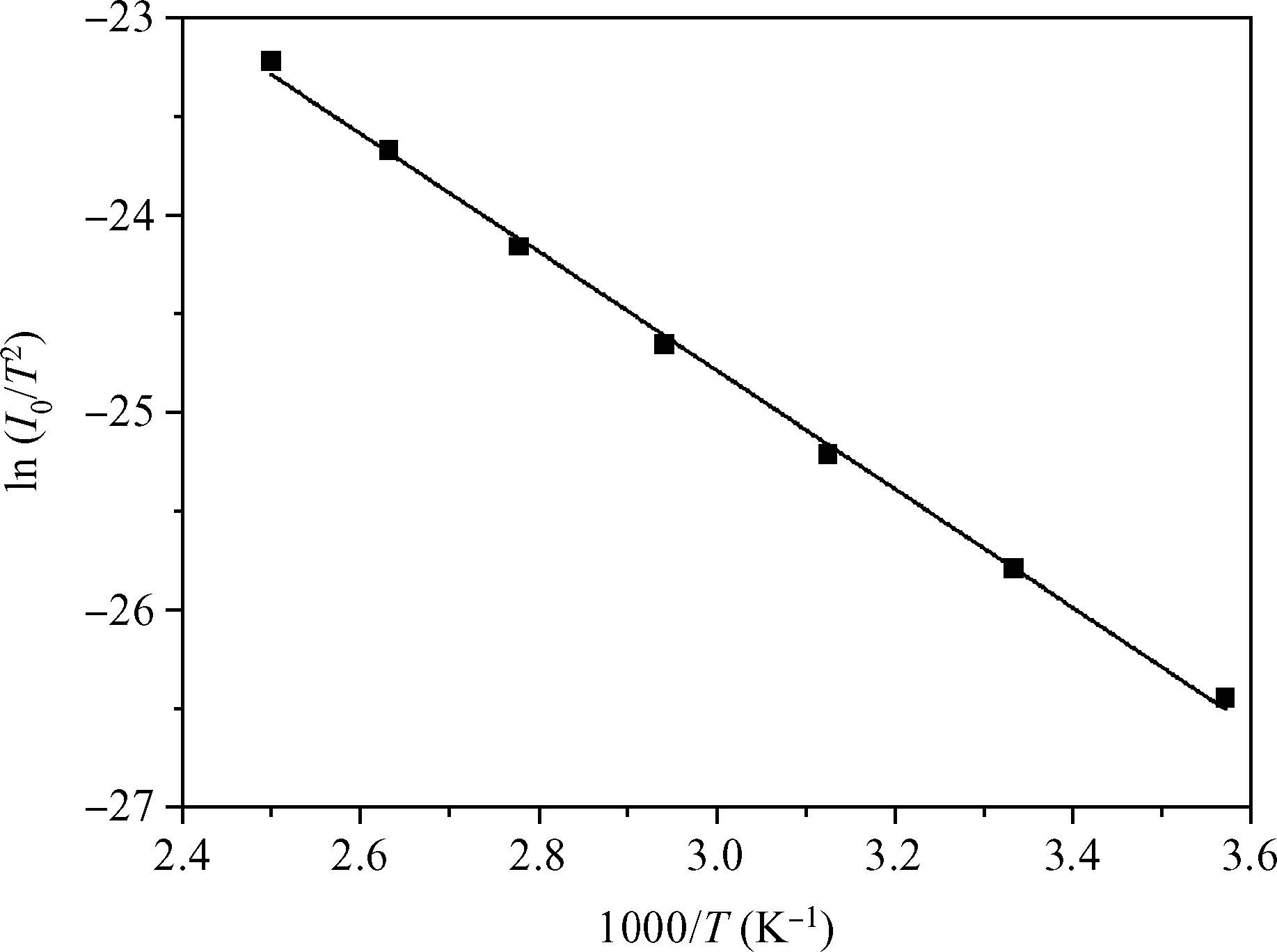
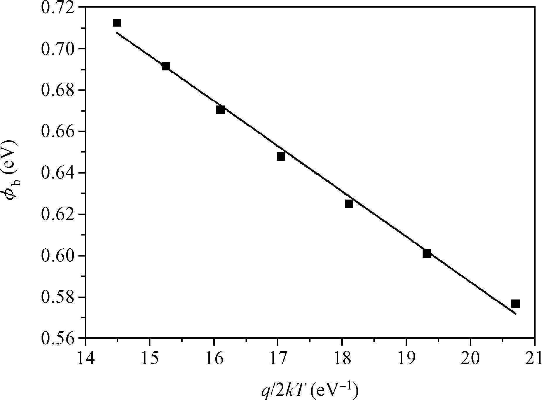


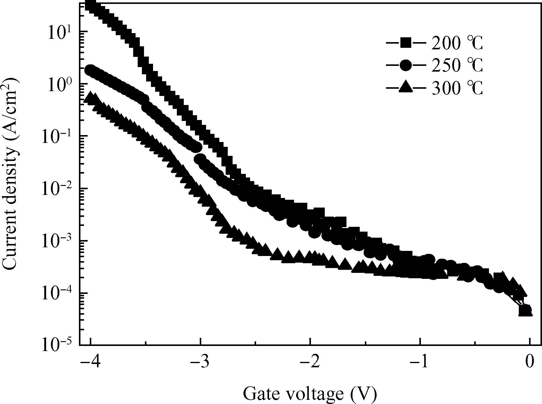
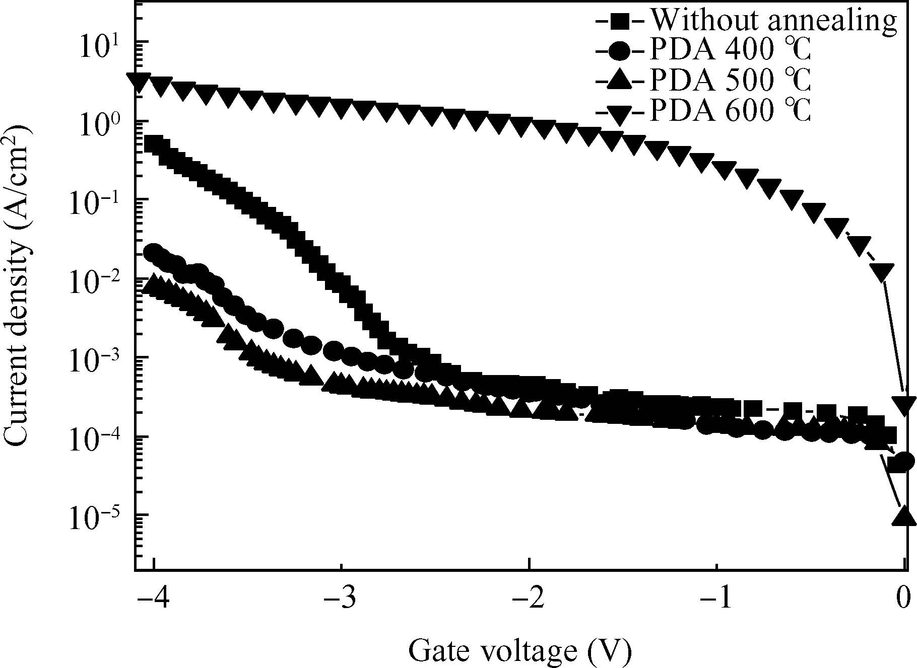
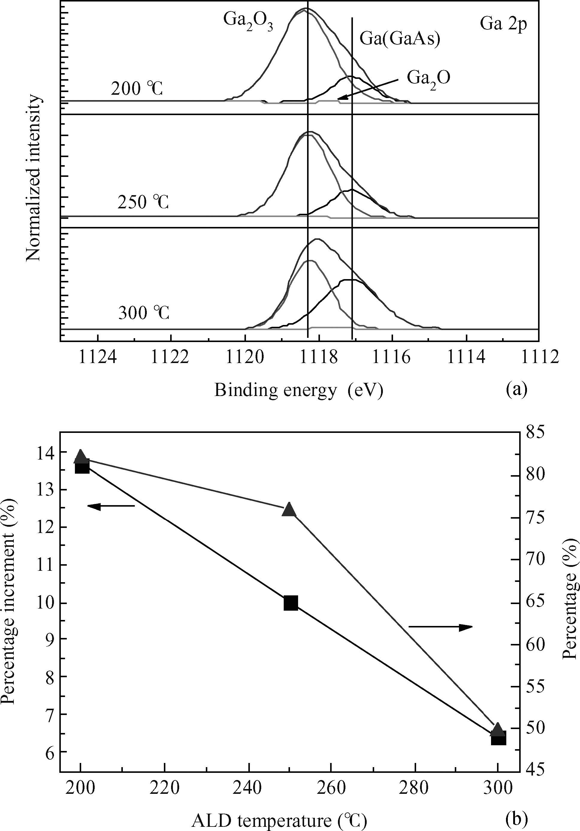
We have investigated the temperature dependent interfacial and electrical characteristics of p-GaAs metal-oxide-semiconductor capacitors during atomic layer deposition(ALD) and annealing of HfO2 using the tetrakis(ethylmethyl) amino hafnium precursor. The leakage current decreases with the increase of the ALD temperature and the lowest current is obtained at 300℃ as a result of the Frenkel-Poole conduction induced leakage current being greatly weakened by the reduction of interfacial oxides at the higher temperature. Post deposition annealing(PDA) at 500℃ after ALD at 300℃ leads to the lowest leakage current compared with other annealing temperatures. A pronounced reduction in As oxides during PDA at 500℃ has been observed using X-ray photoelectron spectroscopy at the interface resulting in a proportional increase in Ga2O3. The increment of Ga2O3 after PDA depends on the amount of residual As oxides after ALD. Thus, the ALD temperature plays an important role in determining the high-k/GaAs interface condition. Meanwhile, an optimum PDA temperature is essential for obtaining good dielectric properties.


This letter proposes a novel IGBT structure with an n-type barrier(NB-IGBT) formed on the silicon surface to enhance the conductivity modulation effect with a relatively simple fabrication process. TCAD simulation indicates that the NB-IGBT offers a current density 49% higher and turn-off losses 25% lower than a conventional field-stop IGBT(FS-IGBT) with a similar breakdown voltage, turn-off time and avalanche energy. Furthermore, the NB-IGBT exhibits extremely large transconductance, which is favorable to turn-on and turn-off. Therefore, the proposed IGBT offers an attractive option for high-voltage and large-power electronics applications.


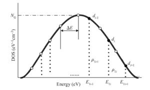
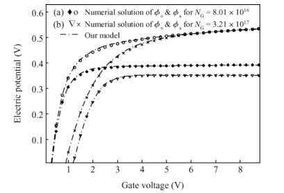
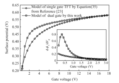
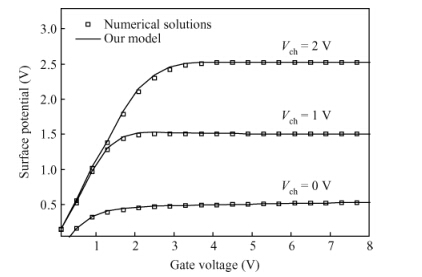
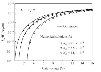
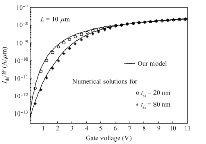
Accounting for the deep Gaussian and tail exponential distribution of the density of states, a physical approximation for potentials of amorphous silicon thin-film transistors using a symmetric dual gate(sDG a-Si:H TFT) has been presented. The proposed scheme provides a complete solution of the potentials at the surface and center of the layer without solving any transcendental equations. A channel current model incorporating features of gate voltage-dependent mobility and coupling factor is derived. We show the parameters required for accurately describing the current-voltage(I-V) characteristics of DG a-Si:H TFT and just how sensitively these parameters affect TFT current. Particularly, the parameters' dependence on the I-V characteristics with respect to the density of deep state and channel thickness has been investigated in detail. The resulting scheme and model are successively verified through comparison with numerical simulations as well as the available experimental data.

Instead of the conventional design with five contacts in the sensor active area, innovative vertical Hall devices(VHDs) with four contacts and six contacts are asymmetrical in structural design but symmetrical in the current flow that can be well fit for the spinning current technique for offset elimination. In this article, a conformal mapping calculation method is used to predict the performance of asymmetrical VHD embedded in a deep n-well with four contacts. Furthermore, to make the calculation more accurate, the junction field effect is also involved into the conformal mapping method. The error between calculated and simulated results is less than 5% for the current-related sensitivity, and approximately 13% for the voltage-related sensitivity. This proves that such calculations can be used to predict the optimal structure of the vertical Hall-devices.
A novel dual-directional silicon controlled rectifier(DDSCR) device with embedded PNP structure(DDSCR-PNP) is proposed for electrostatic discharge(ESD) protection, which has greatly reduced latch-up risk owing to the improved holding voltage(Vh). Firstly, the working mechanism of the DDSCR-PNP is analyzed. The theoretical analysis indicates that the proposed device possesses good voltage clamp ability due to the embedded PNP(PNP_2). Then, experimental devices are fabricated in a 0.35μm bipolar-CMOS-DMOS process and measured with a Barth 4002 transmission line pulse testing system. The results show that the Vh of DDSCR-PNP is much higher than that of the conventional DDSCR, and can be further increased by adjusting the P well width. However, the reduced leakage current(IL) of the DDSCR-PNP shows obvious fluctuations when the P well width is increased to more than 12μm. Finally, the factors influencing Vh and IL are investigated by Sentaurus simulations. The results verify that the lateral PNP_2 helps to increase Vh and decrease IL. When the P well width is further increased, the effect of the lateral PNP_2 is weakened, causing an increased IL. The proposed DDSCR-PNP provides an effective and attractive ESD protection solution for high-voltage integrated circuits.
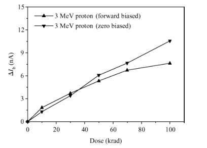
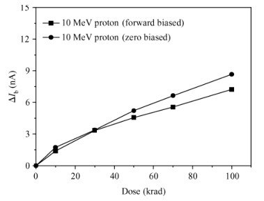
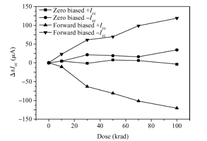
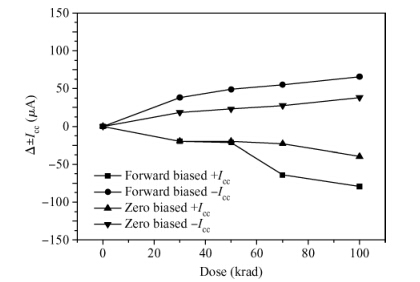
NPN-input bipolar operational amplifiers LM741 were irradiated with 60Co γ-ray, 3 MeV protons and 10 MeV protons respectively at different biases to investigating the proton radiation response of the NPN-input operational amplifier. The comparison of protons with 60Co γ-rays showed that the proton radiation mainly induced ionization damage in LM741. Under different bias conditions, the radiation sensitivity is different; zero biased devices show more radiation sensitivity in the input biased current than forward biased devices. Supply current(±Icc) is another parameter that is sensitive to proton radiation, 60Co γ-ray, 3 MeV and 10 MeV proton irradiation would induce a different irradiation response in ±Icc, which is caused by different ionization energy deposition and displacement energy deposition of 60Co γ-ray, 3 MeV and 10 MeV proton irradiation.

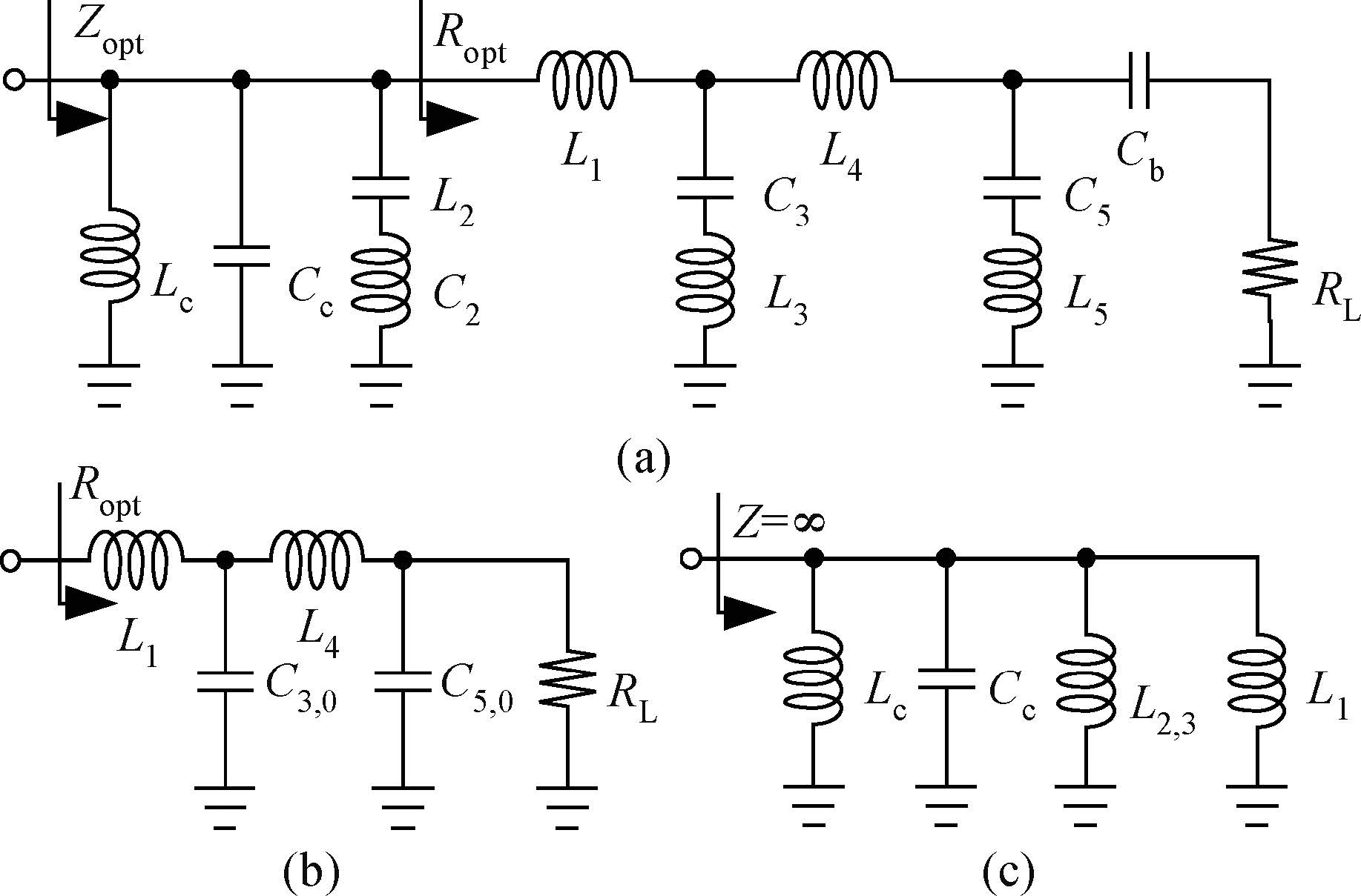
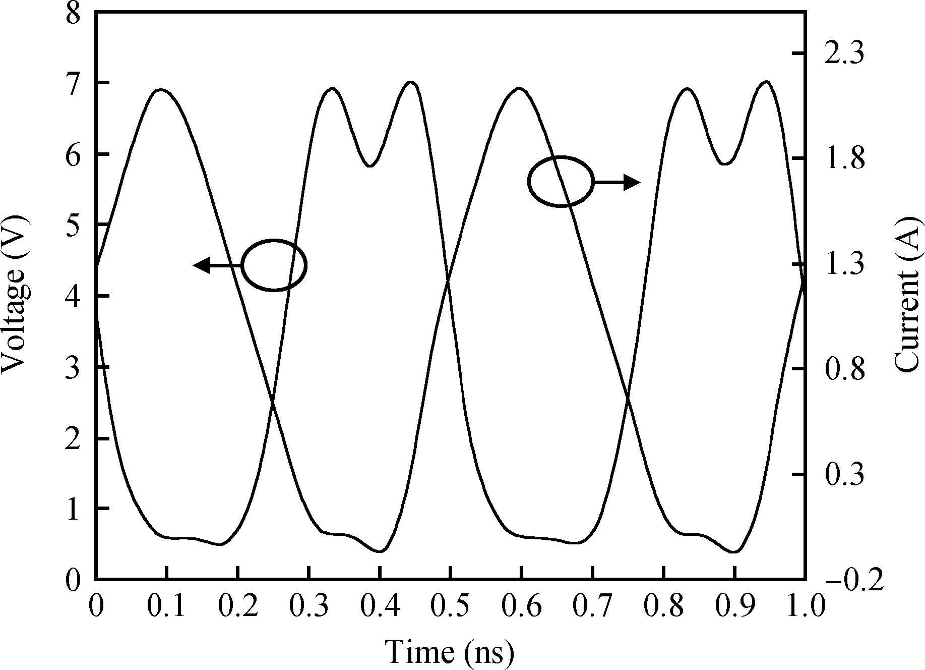
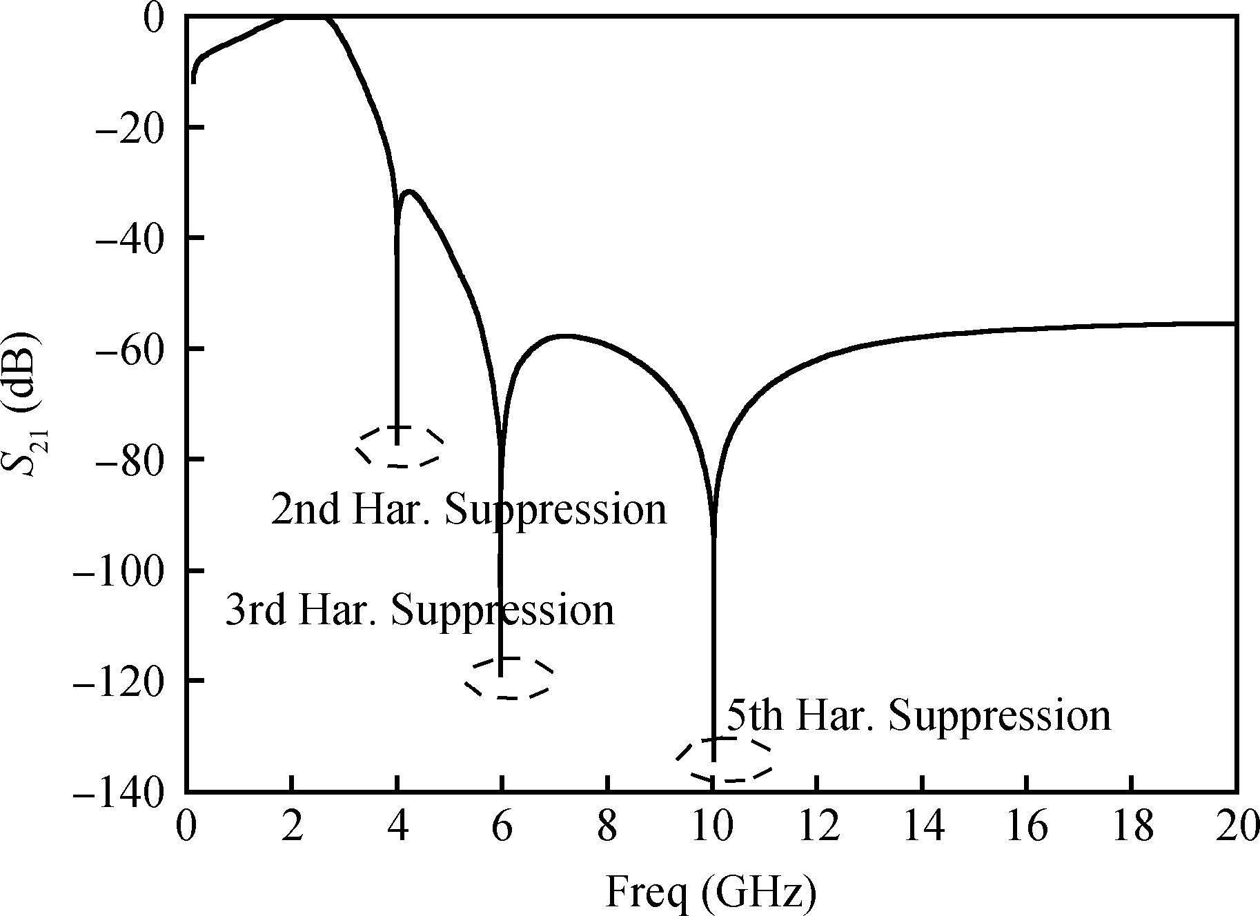
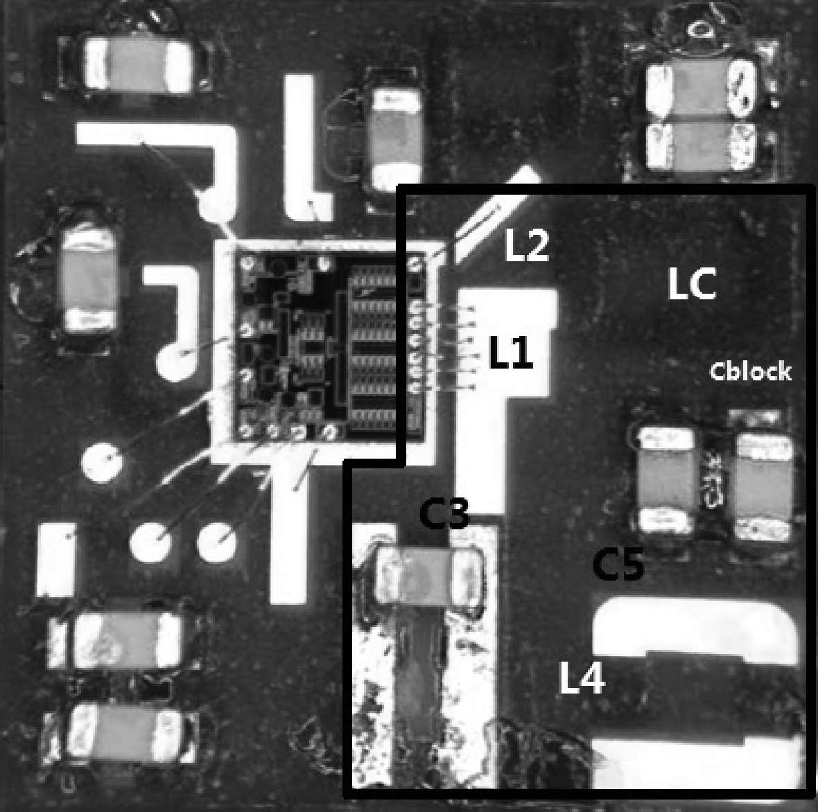
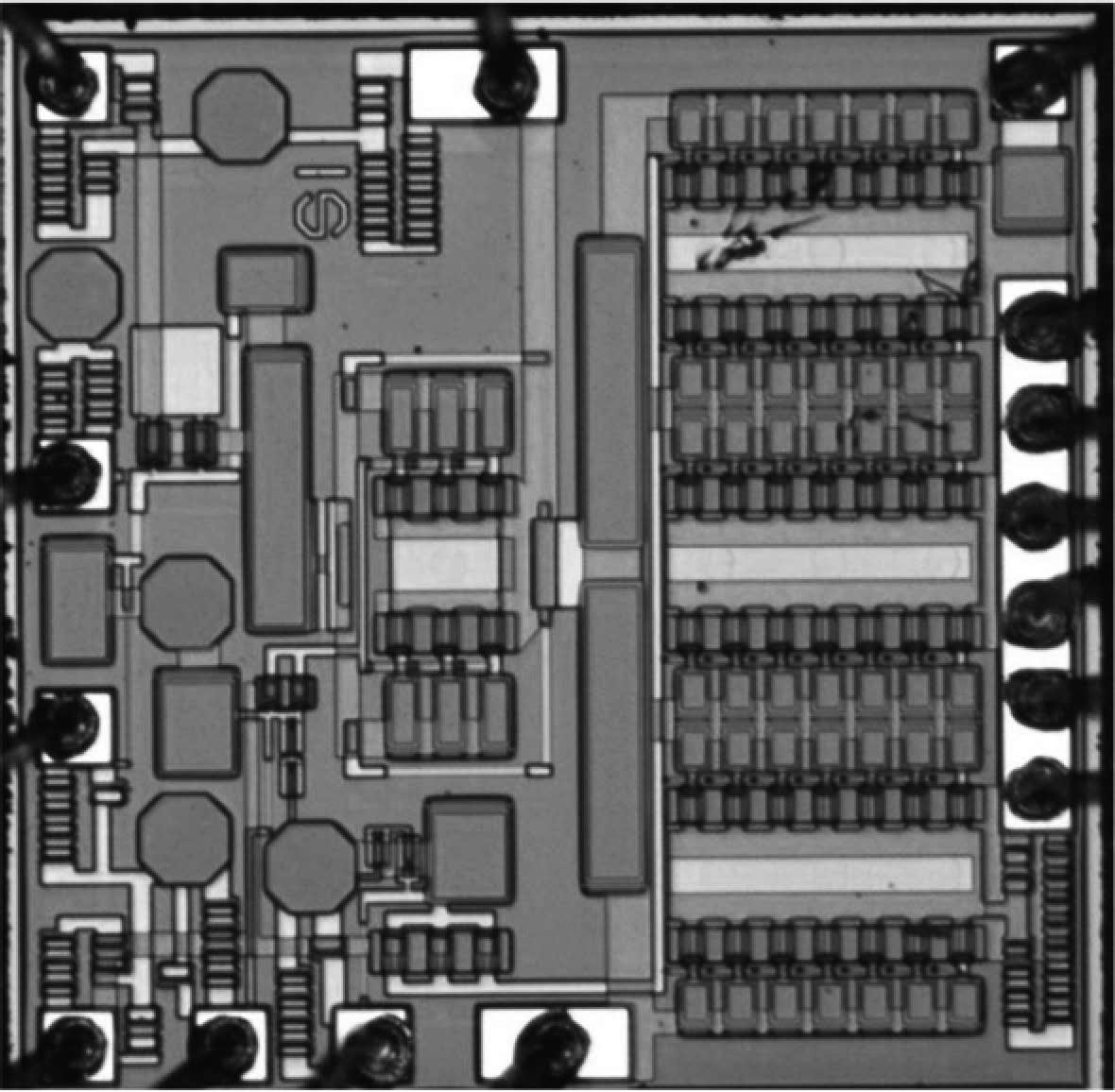
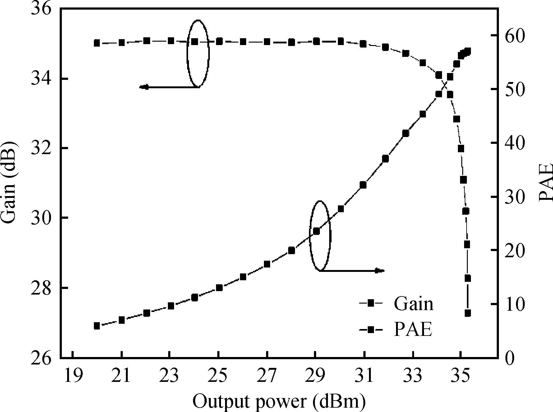
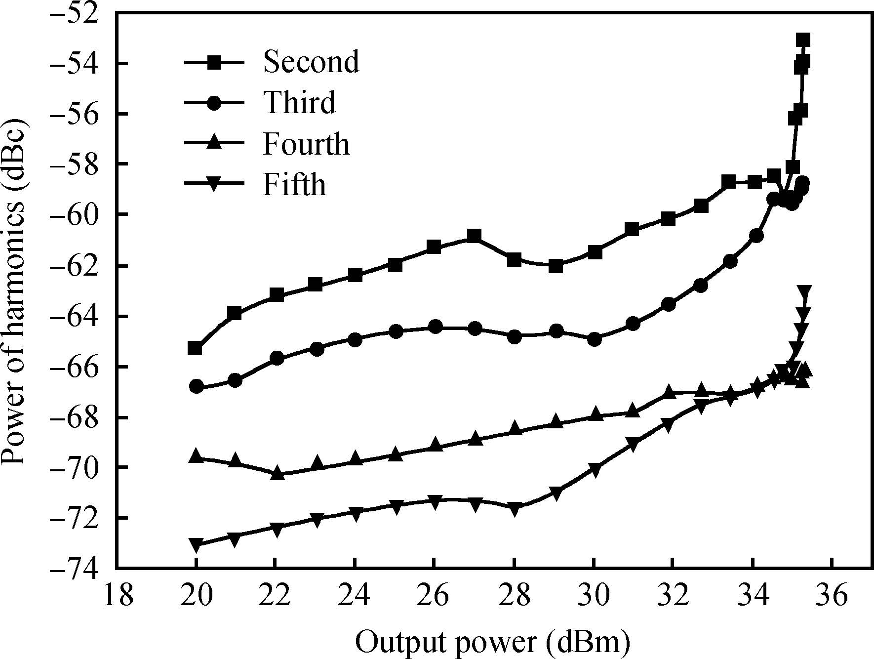
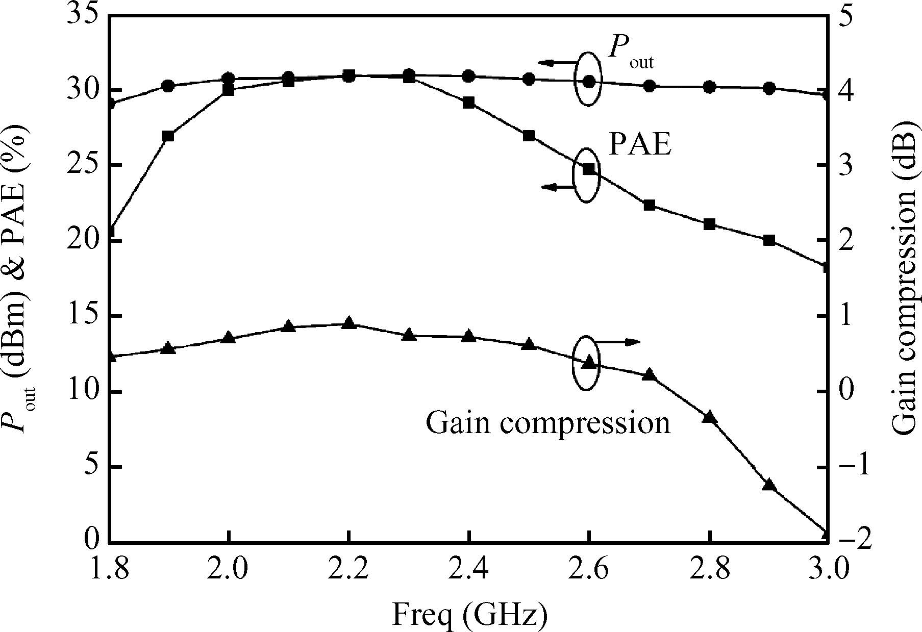
A broadband class-F power amplifier for an S-band handset device is integrated on a 3×3×0.82 mm3 die using an InGaP/GaAs HBT process. With LC serial harmonic traps immersed into the broadband output matching circuit, good harmonic suppression performance can be achieved. A pure resistive impedance of the matching circuit, but near zero at second and infinite at third harmonic frequency, which enhances the efficiency, is obtained across 1.8-2.5 GHz. Tested with a continuous wave(CW) signal, the PA delivers an output power of 34 dBm and achieves a PAE of 57% at 2 GHz. In addition, excellent harmonic suppression levels of less than-53 dBc across the second to fifth harmonic are obtained.


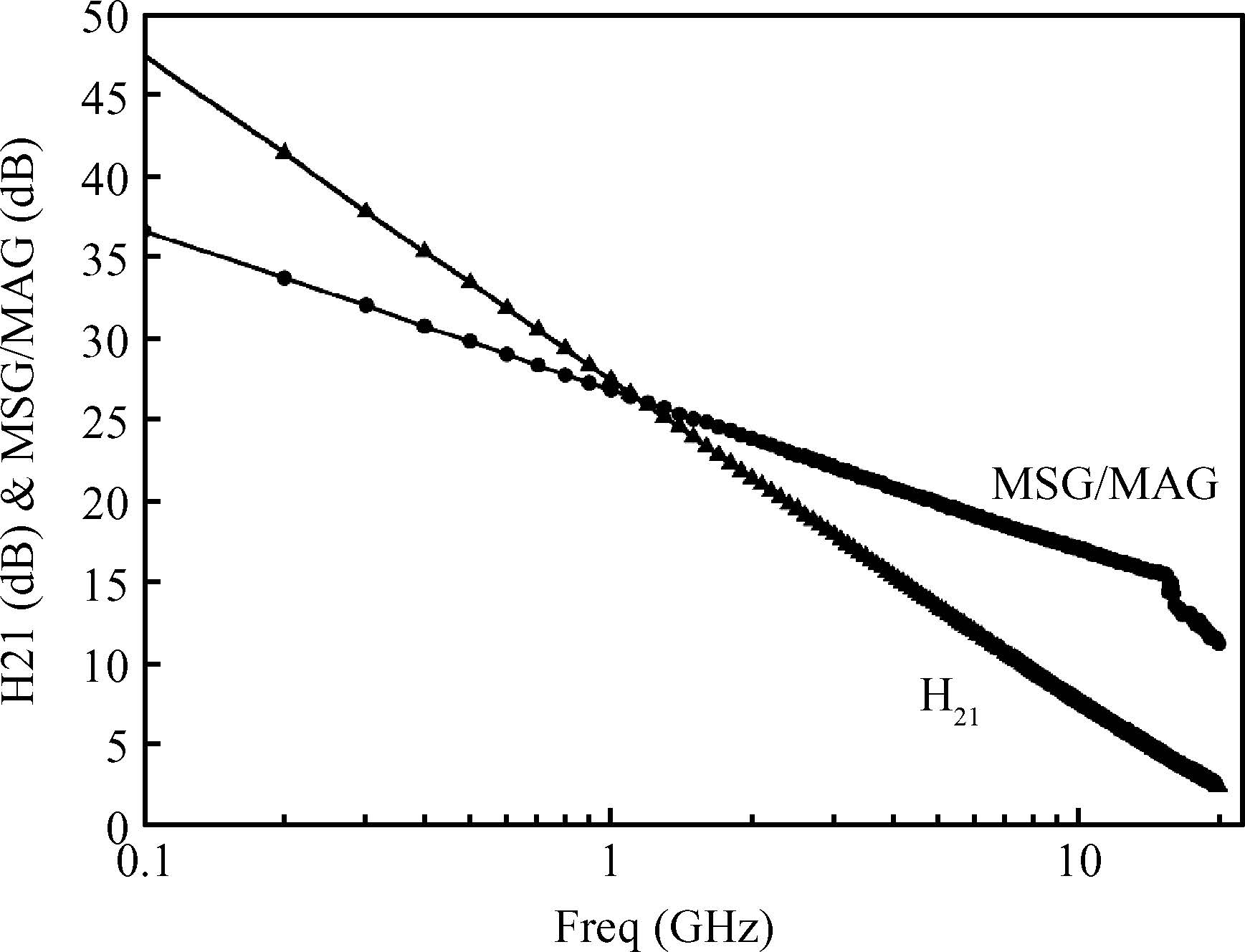
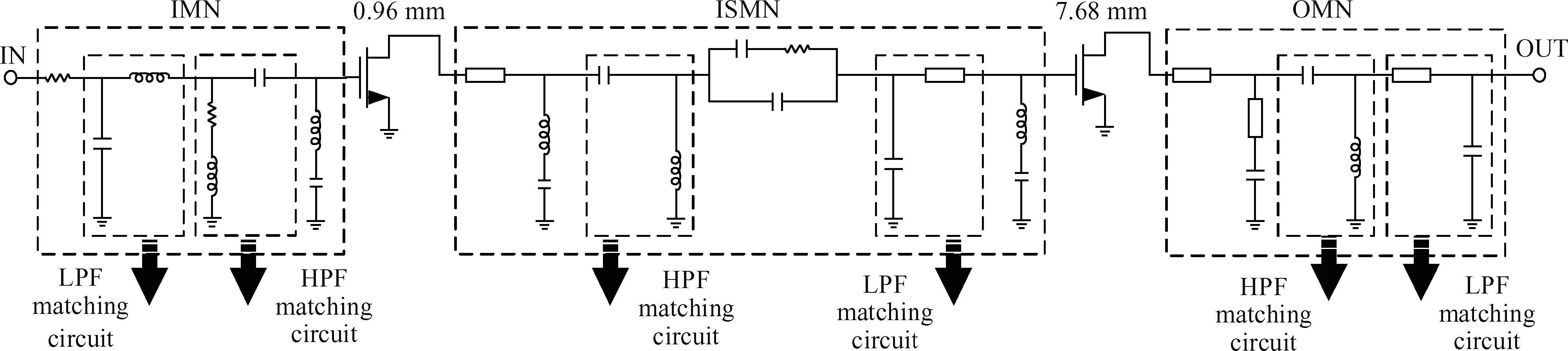
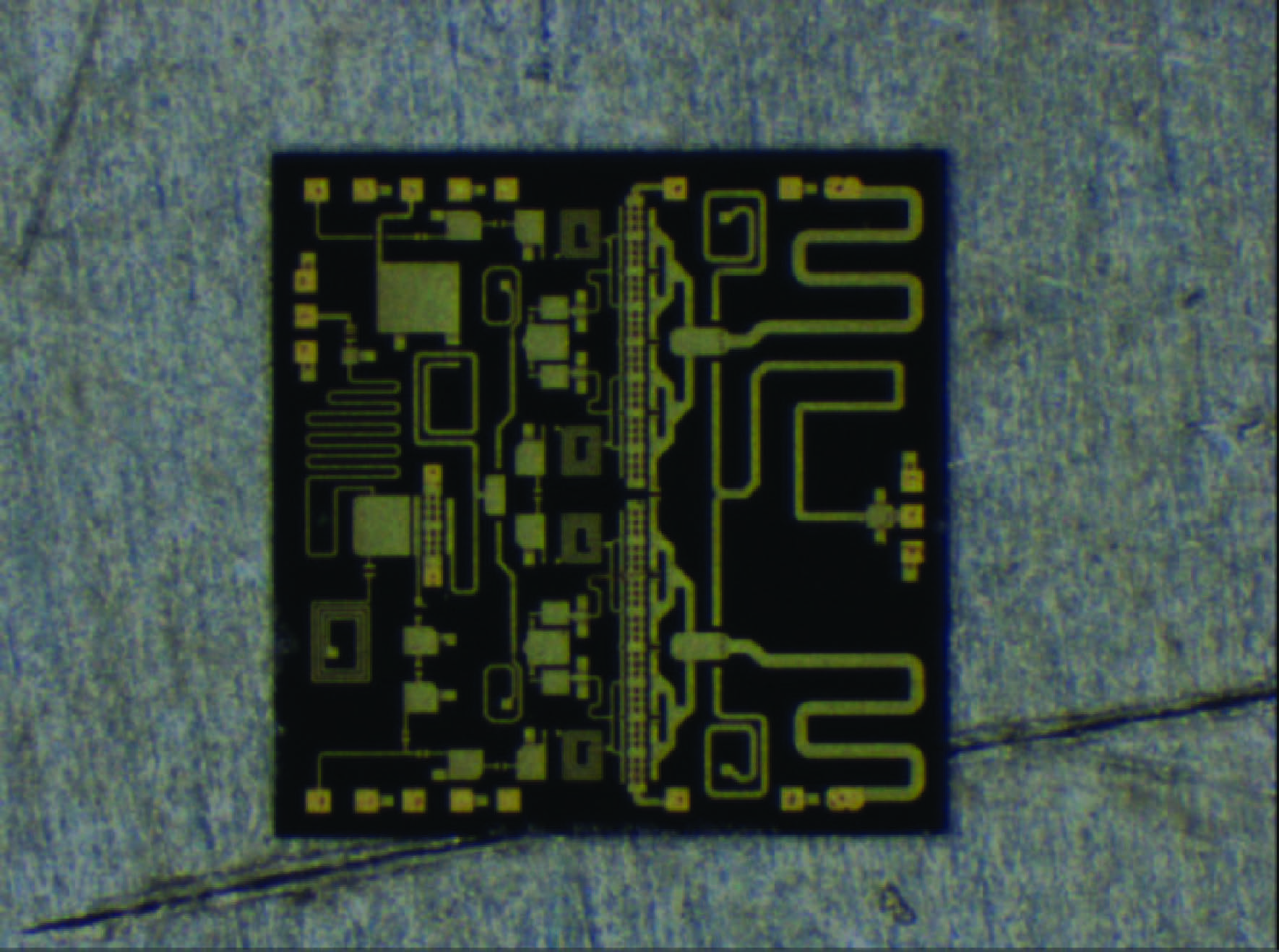
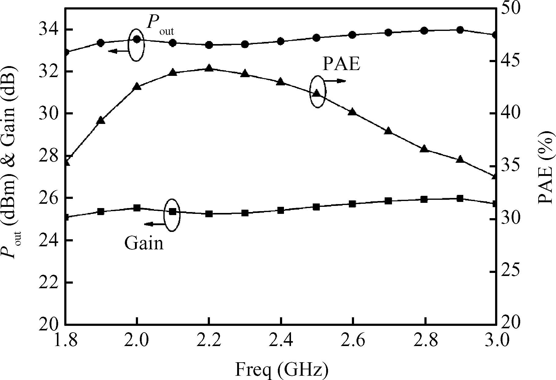
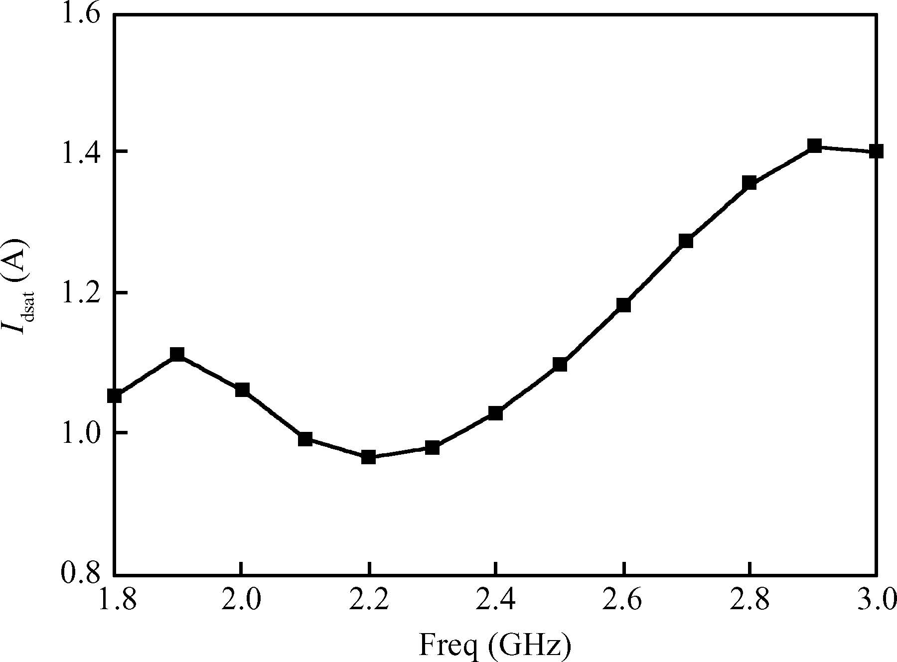
This paper describes an S-band wideband high efficiency power amplifier based on the Nanjing Electron Device Institute's GaAs pHEMT monolithic microwave integrated circuit(MMIC) technology. To realize high efficiency, the two stage power amplifier is designed with a driver ratio of 1:8. The low-pass filter/high-pass filter combined matching circuit is applied to the amplifier to reduce the chip size, as well as to realize the optimum impedances over a wide bandwidth for high efficiency at each stage. Biased at class AB under a drain supply voltage of 5 V, the amplifier delivers 33-34 dBm saturated output power across the frequency range of 1.8 to 3 GHz with associated power-added efficiency of 35%-45% and very flat power gain of 25-26 dB in CW mode. The size of this MMIC is very compact with 2.7×2.75 mm2.

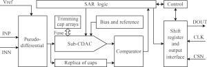
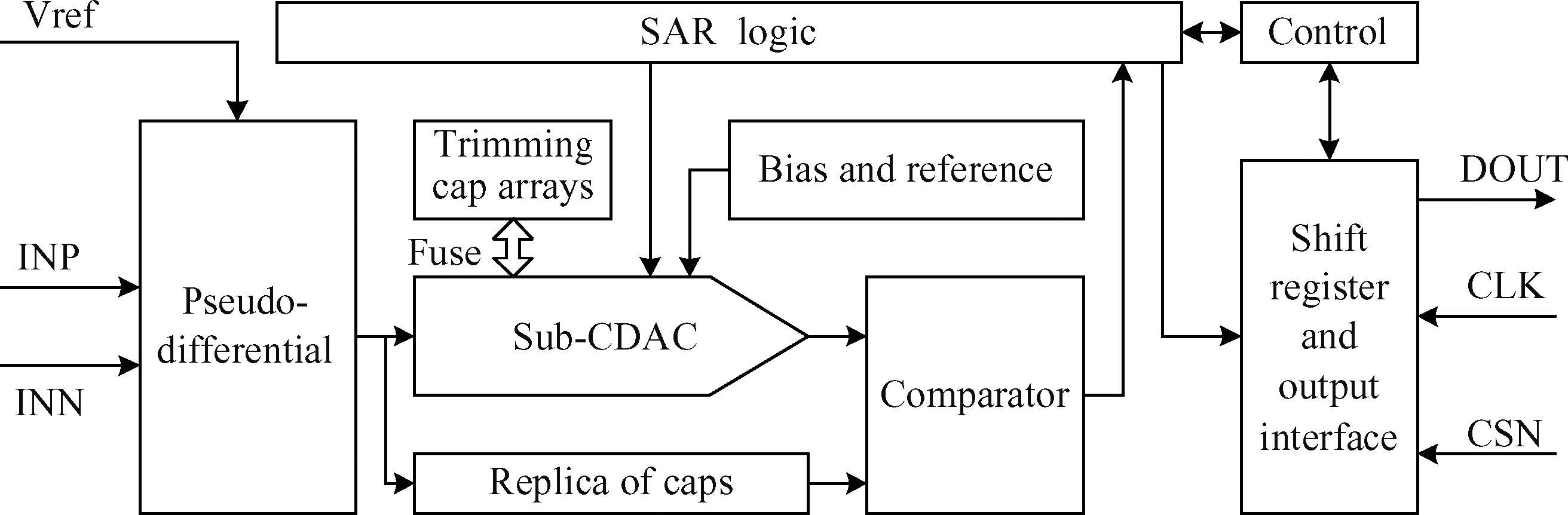
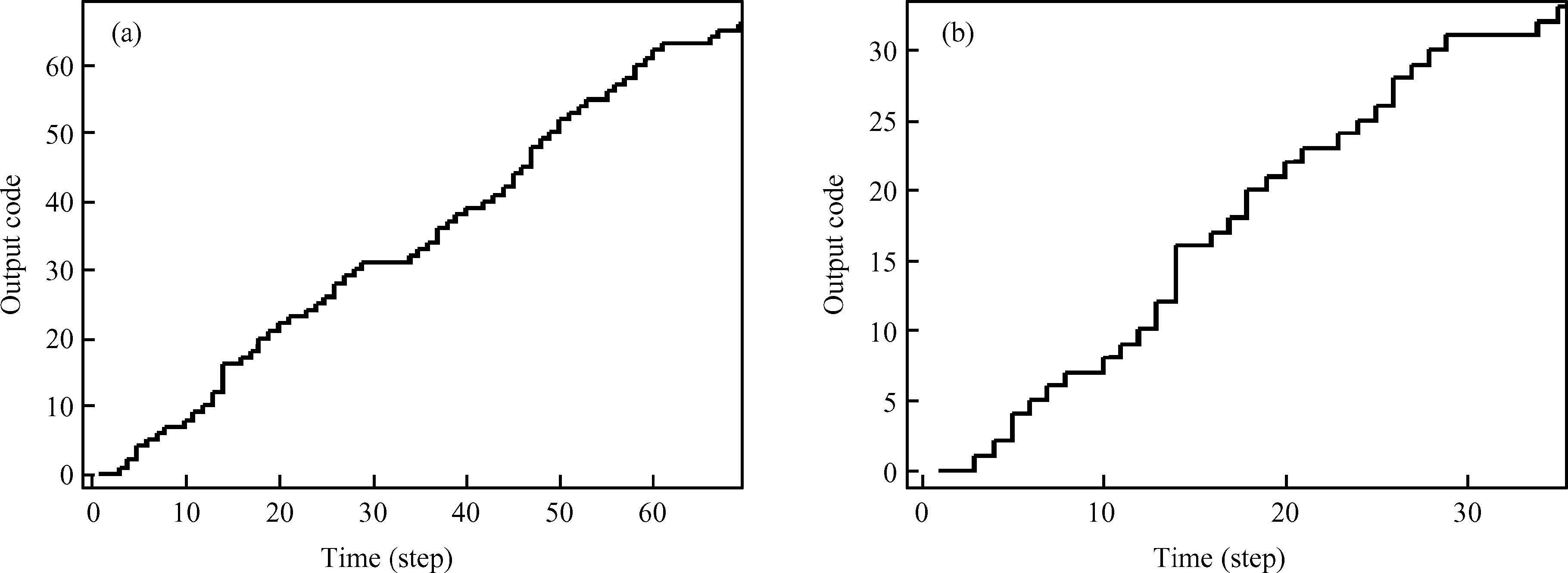
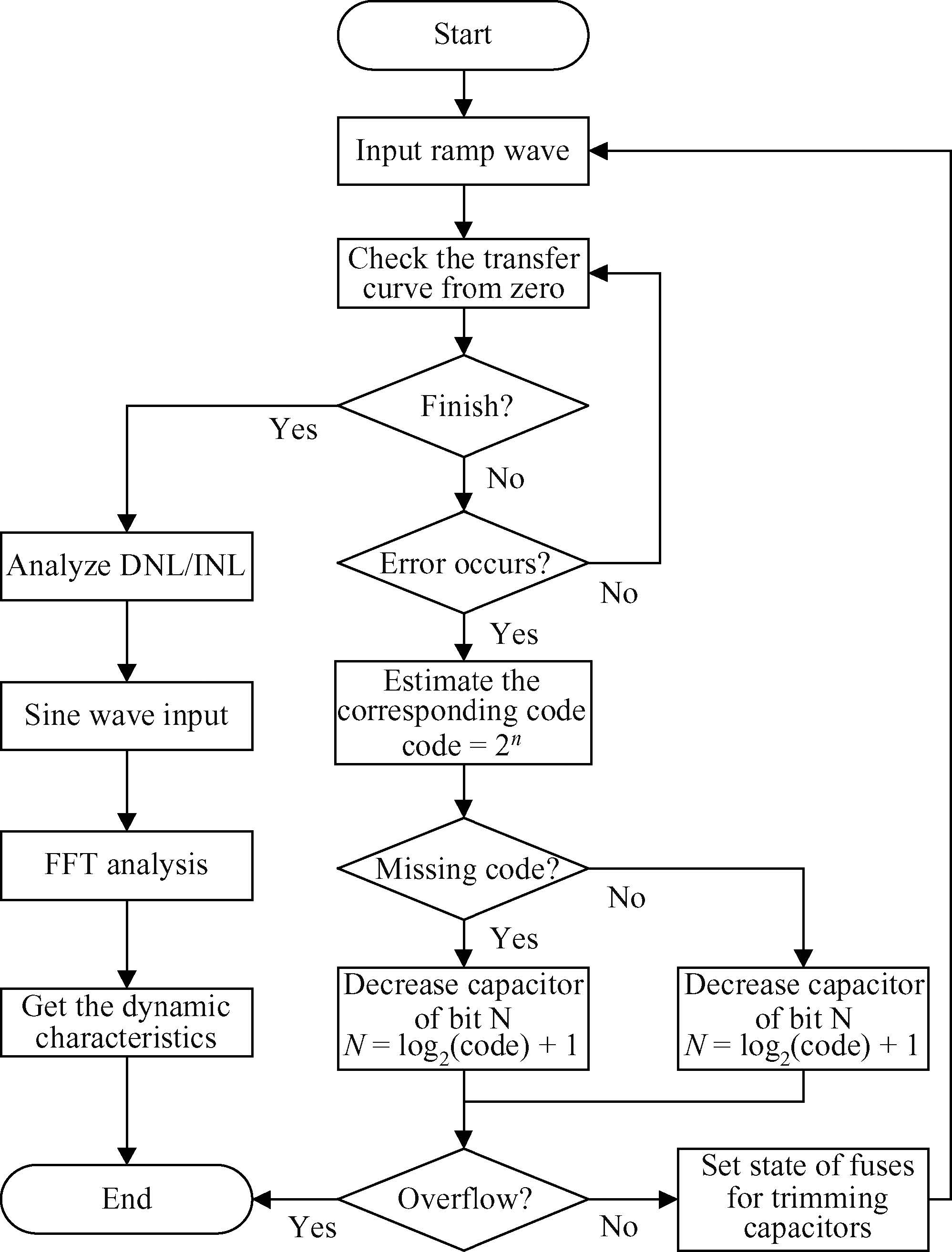
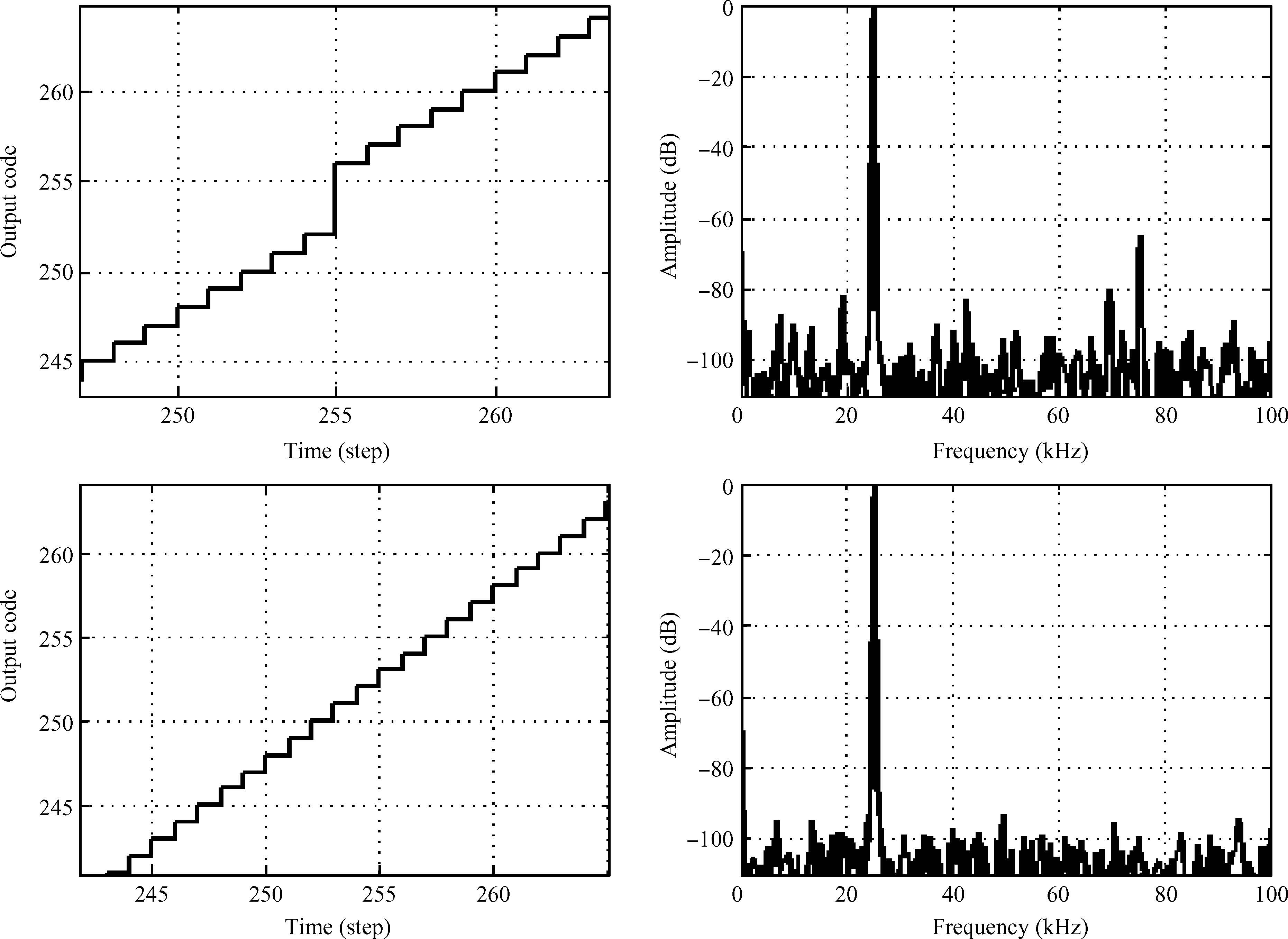
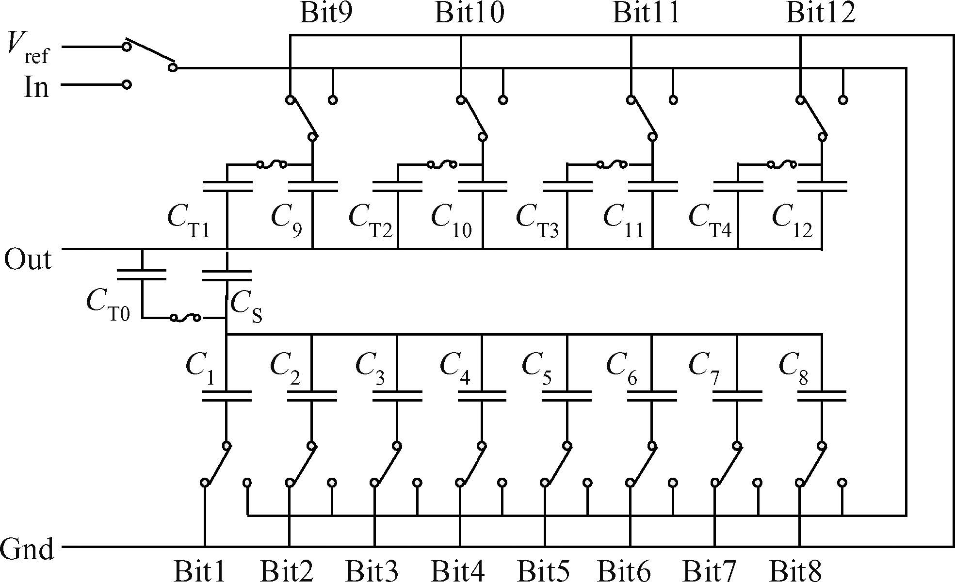
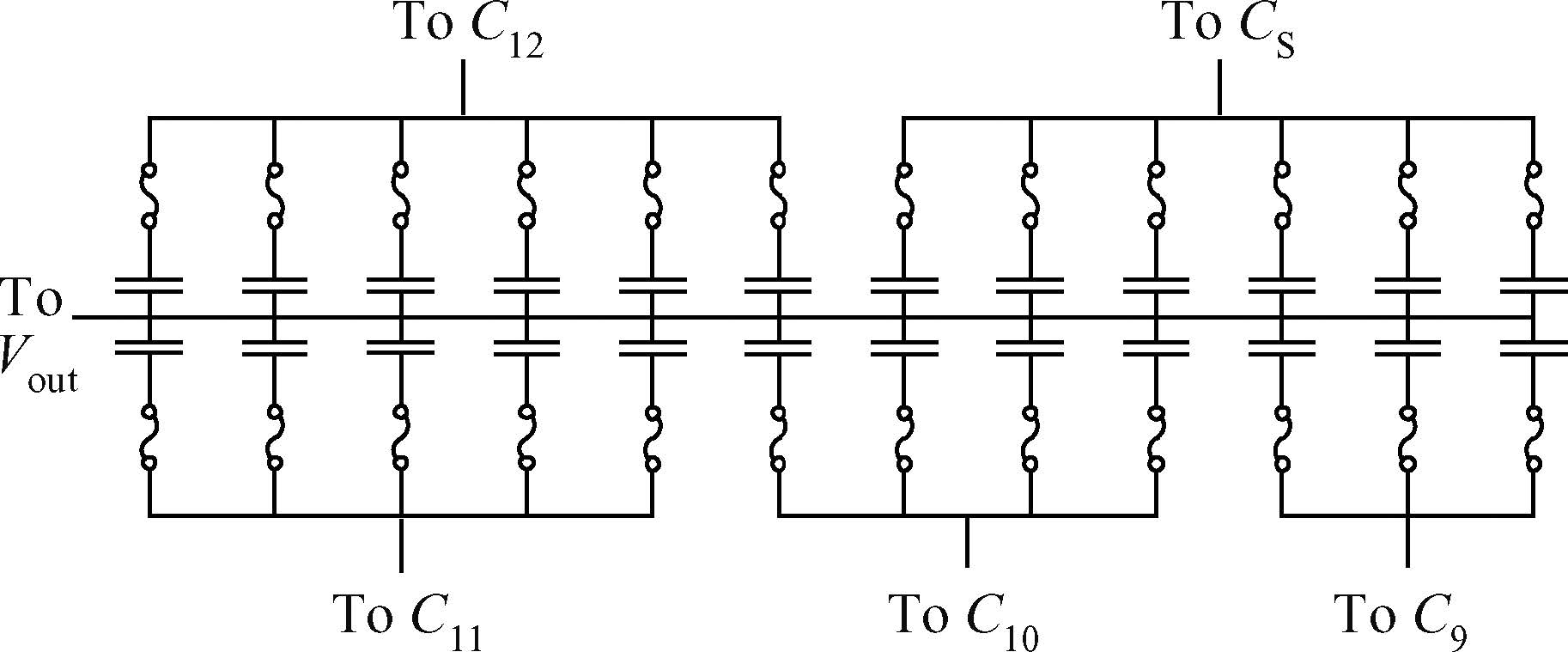
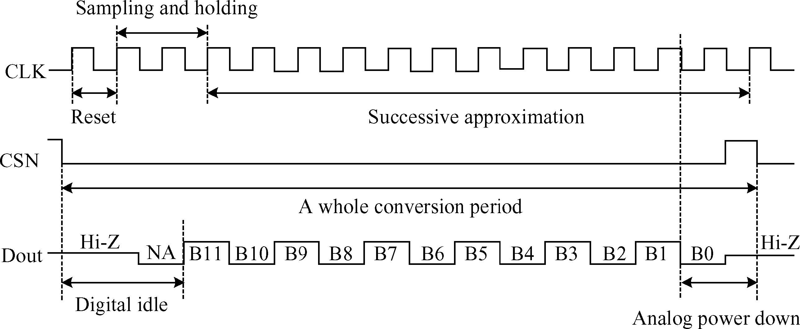
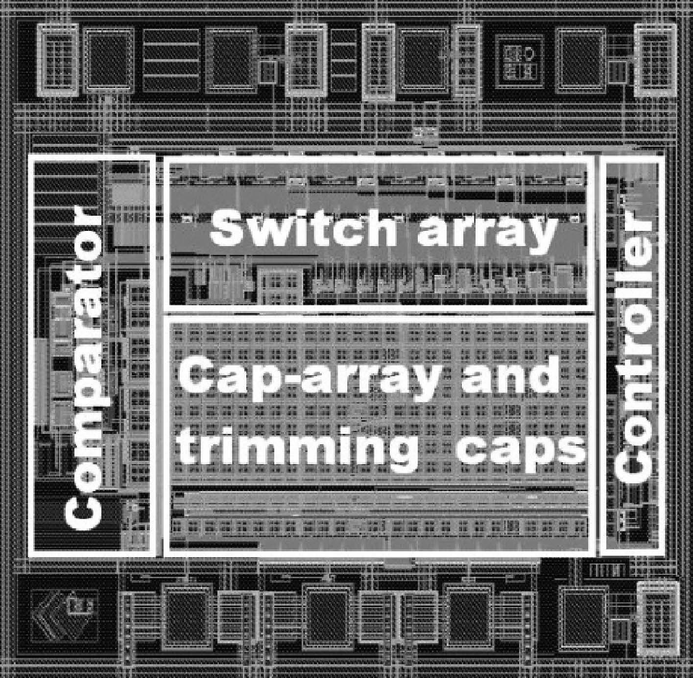
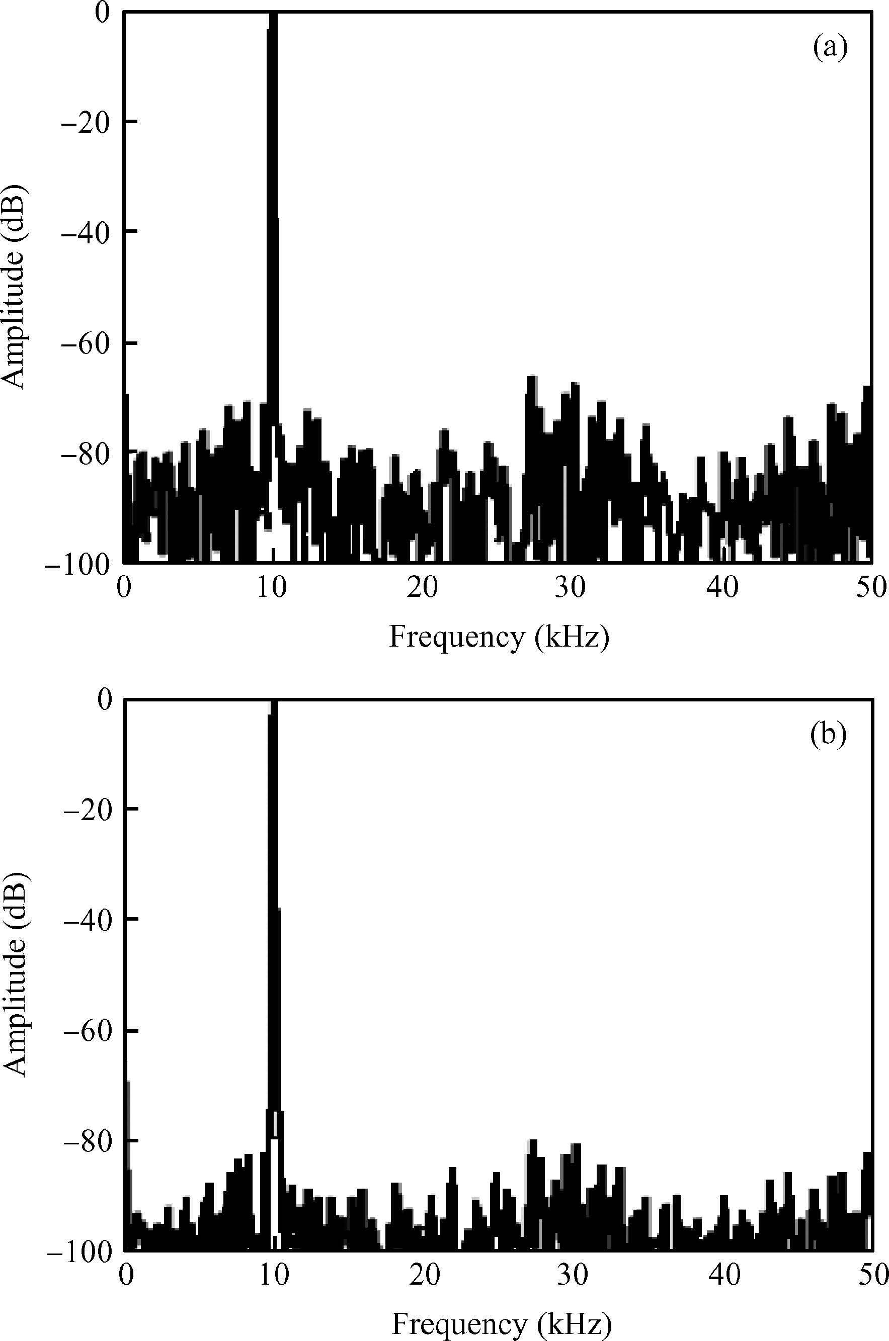
This work presented a trimming technique and algorithm applied in a capacitive successive approximation register(SAR) analog to digital converter(ADC) for a sensor interface, which can be integrated with the preceding sensor and the following controlling circuit. Without spending a special calibration phase or adding complicated functions, this circuit keeps a 12-bit resolution by trimming the capacitor array. Its merits of low power and small area make it suitable to be embedded in a power and cost sensitive system such as a battery-supplied sensor network node. The prototype 12-bit ADC is implemented by 0.5μm 2P3M CMOS technology, with the wide supply range of 2-5 V, its power consumption is only 300μA at a sampling speed of 200 kHz.


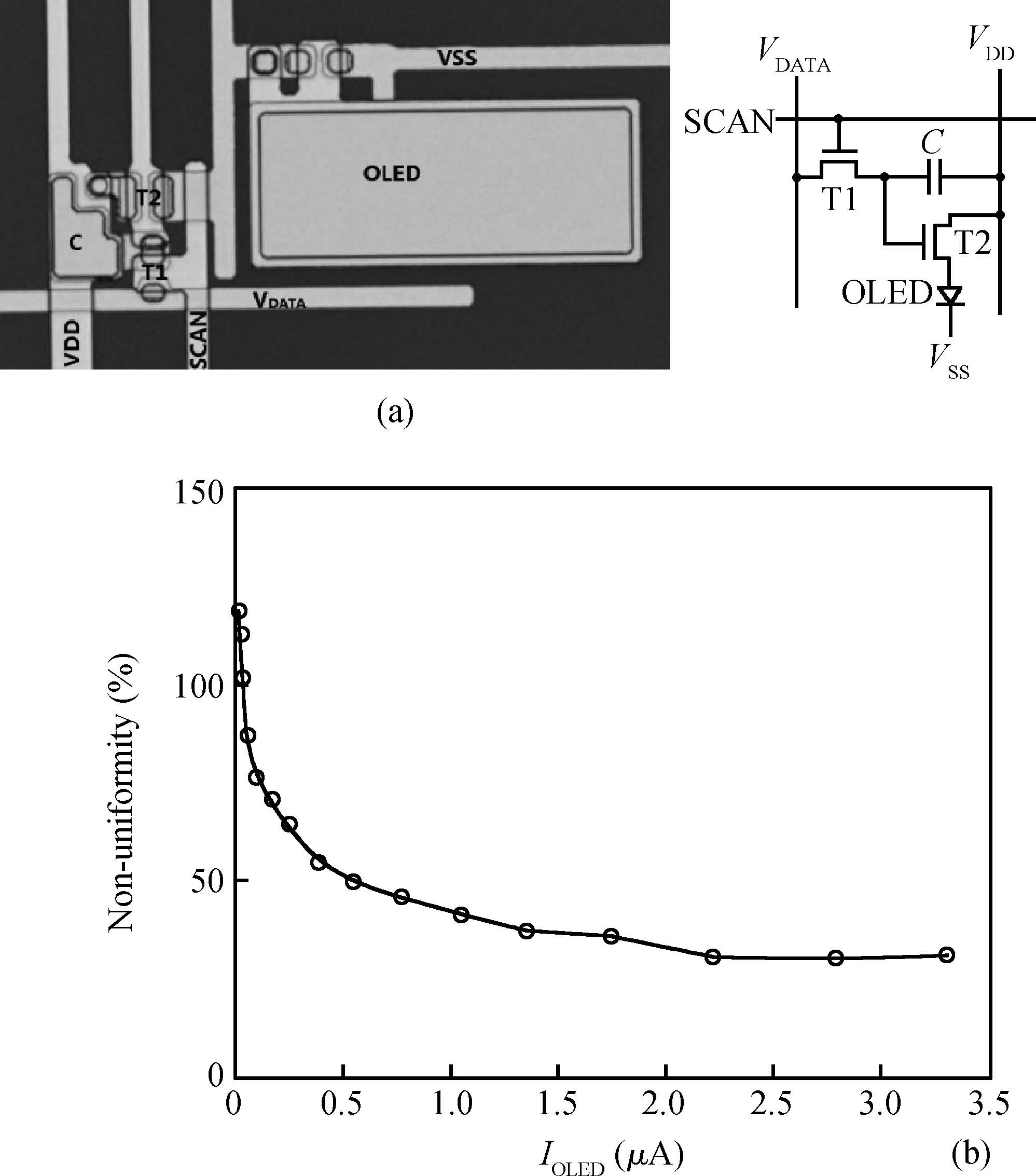
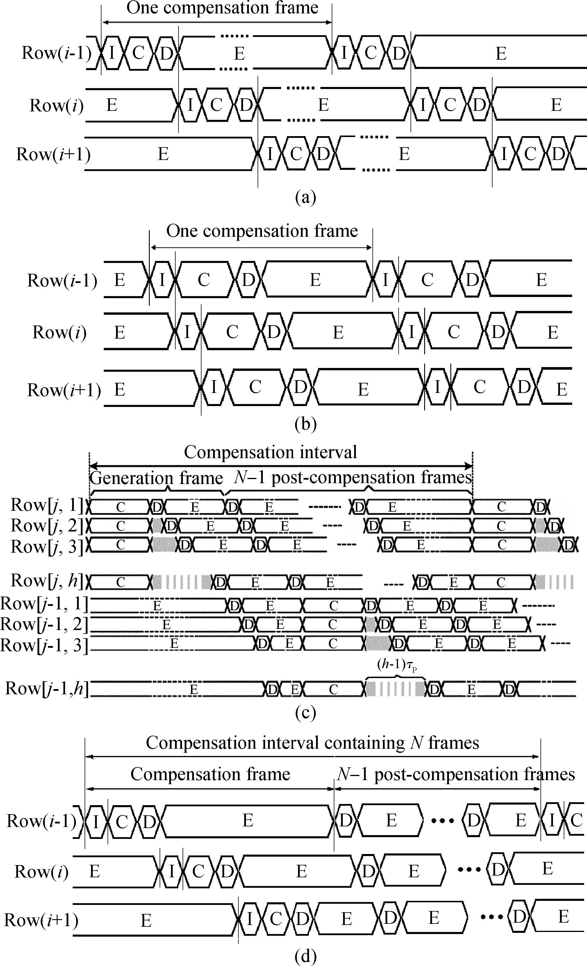
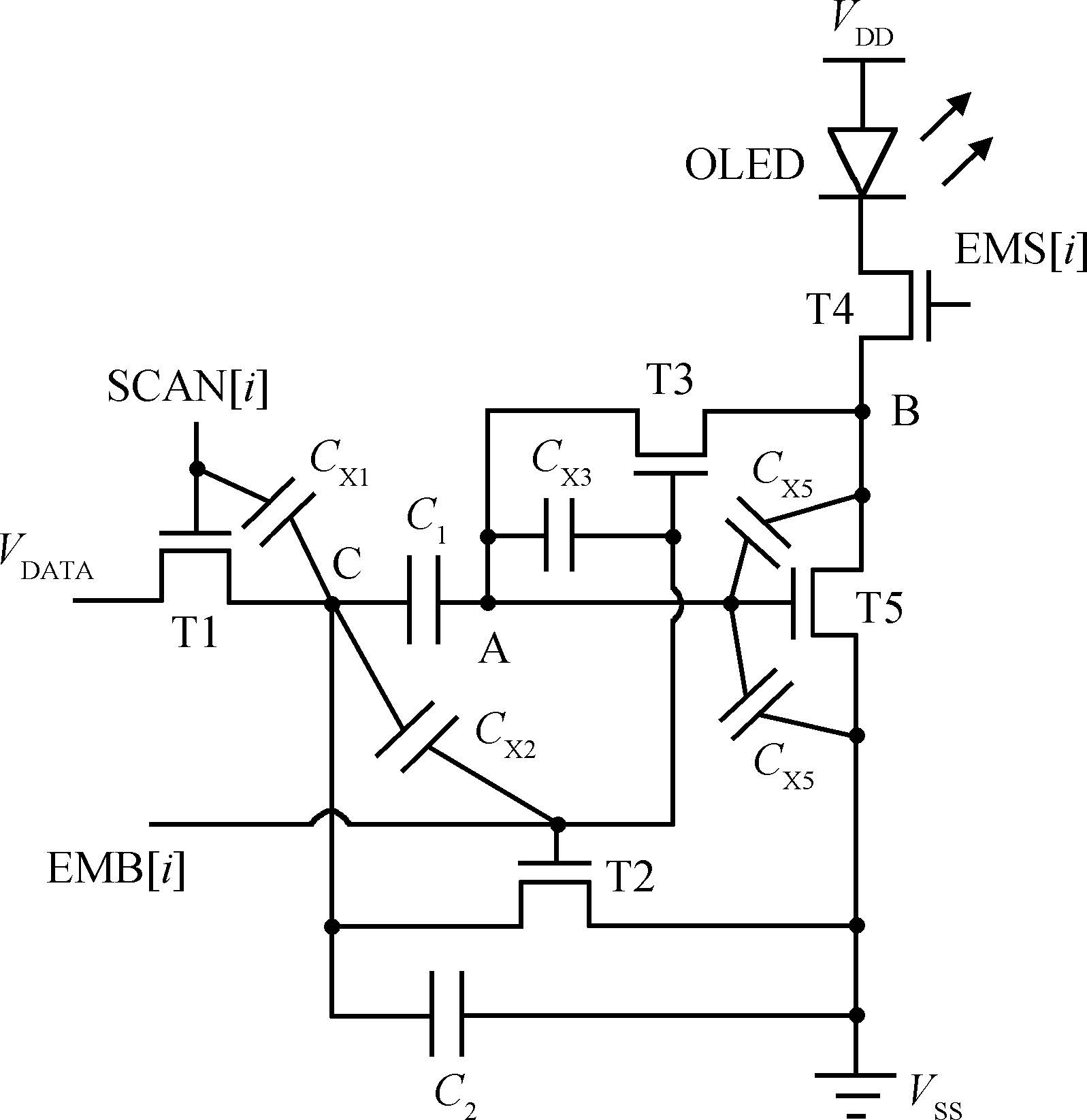
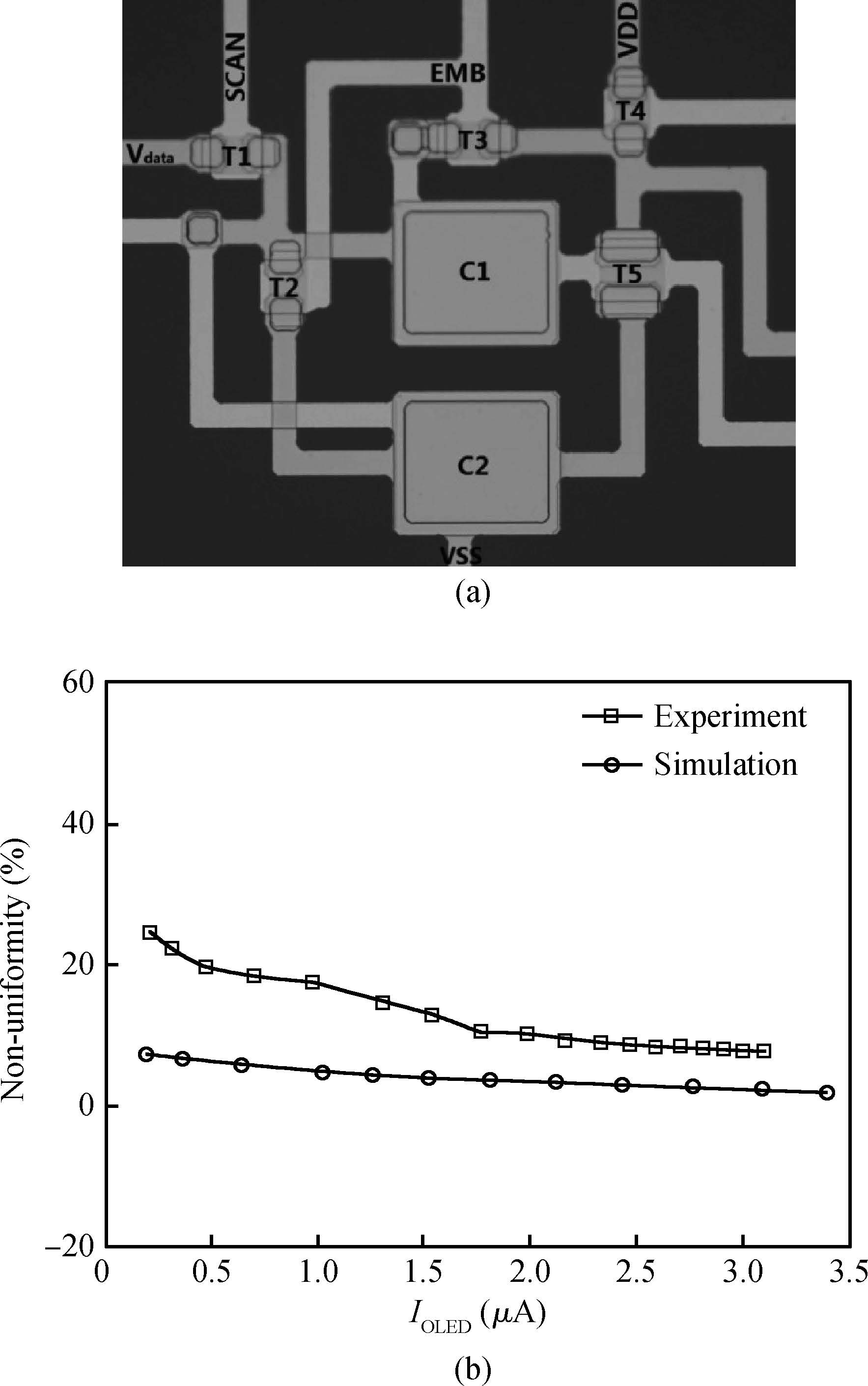
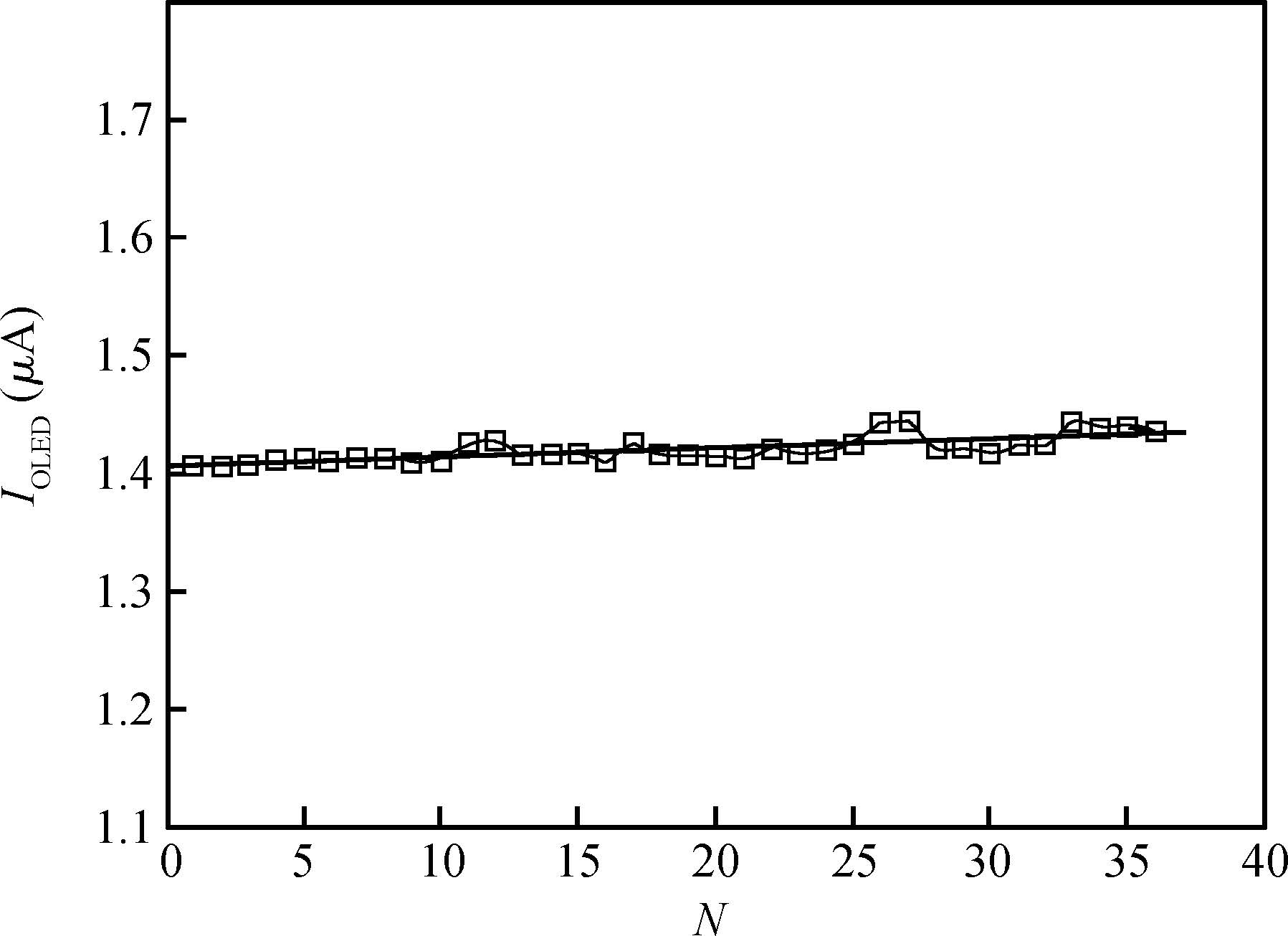
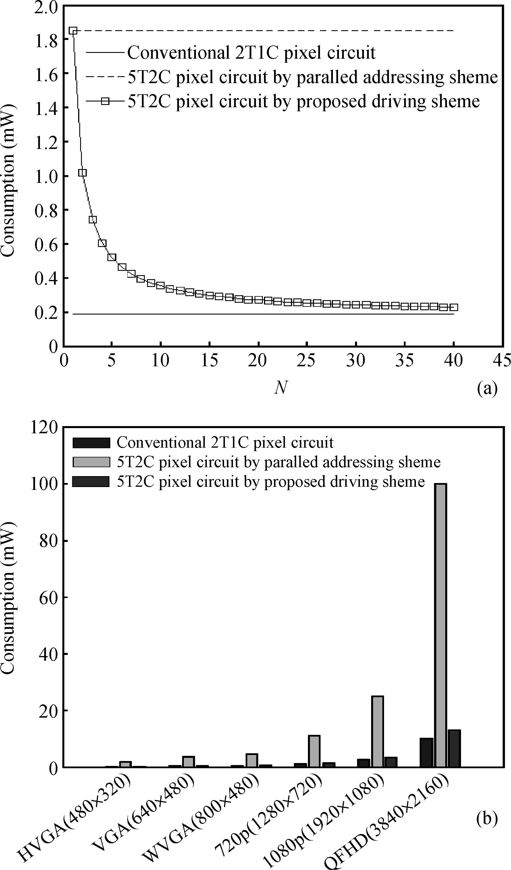
A new voltage-programmed driving scheme named the mixed parallel addressing scheme is presented for AMOLED displays, in which one compensation interval can be divided into the first compensation frame and the consequent N-1 post-compensation frames without periods of initialization and threshold voltage detection. The proposed driving scheme has the advantages of both high speed and low driving power due to the mixture of the pipeline technology and the threshold voltage one-time detection technology. Corresponding to the proposed driving scheme, we also propose a new voltage-programmed compensation pixel circuit, which consists of five TFTs and two capacitors(5T2C). In-Zn-O thin-film transistors(IZO TFTs) are used to build the proposed 5T2C pixel circuit. It is shown that the non-uniformity of the proposed pixel circuit is considerably reduced compared with that of the conventional 2T1C pixel circuit. The number of frames(N) preserved in the proposed driving scheme are measured and can be up to 35 with the variation of the OLED current remaining in an acceptable range. Moreover, the proposed voltage-programmed driving scheme can be more valuable for an AMOLED display with high resolution, and may also be applied to other compensation pixel circuits.


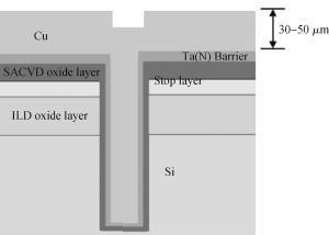
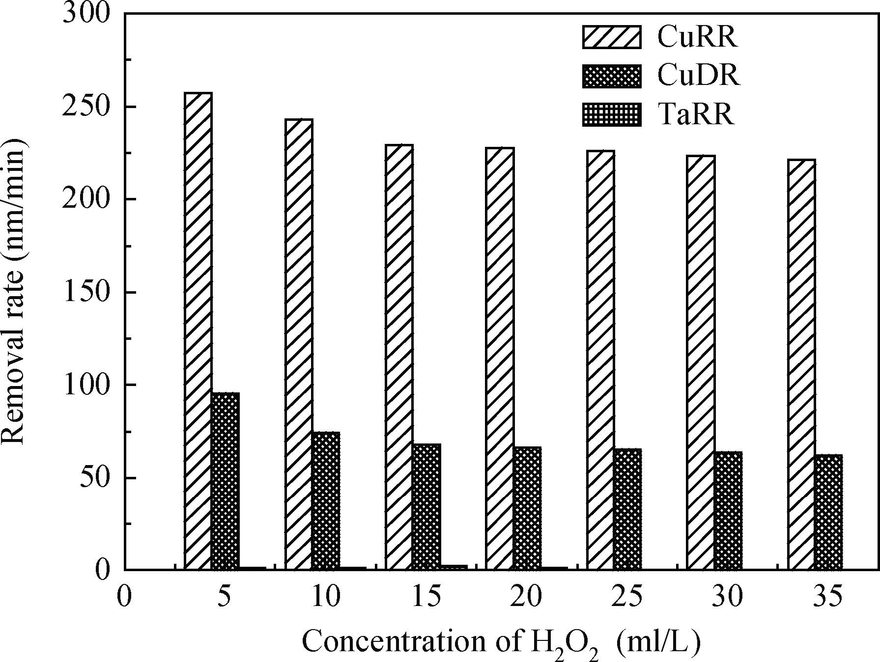
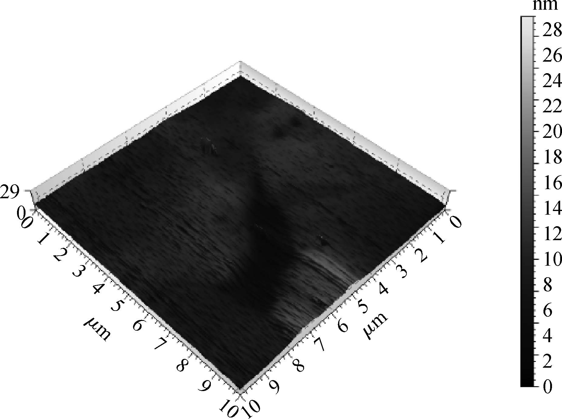
TSV(through silicon via) is an emerging technology, which can realize micromation compared with the conventional packaging and extend Moore's law. Chemical mechanical polishing(CMP) is one of the most important steps in the process of TSV manufacture, and it is an enabling technology to extend Moore's law in the past two decades. Low pressure, low abrasive and low pH value are the main requirements for copper interconnection. In this paper, the effect of different kinds of TSV slurry with FA/O Ⅱ or FA/O IV type chelating agent on CMP are studied. All kinds of slurry used in this study are alkaline with no added inhibitors. From the experiment results, it can be seen that the copper removal rate and surface roughness achieved by using the FA/O IV type chelating agent with a low pH value is superior to using the FA/O Ⅱ type chelating agent.

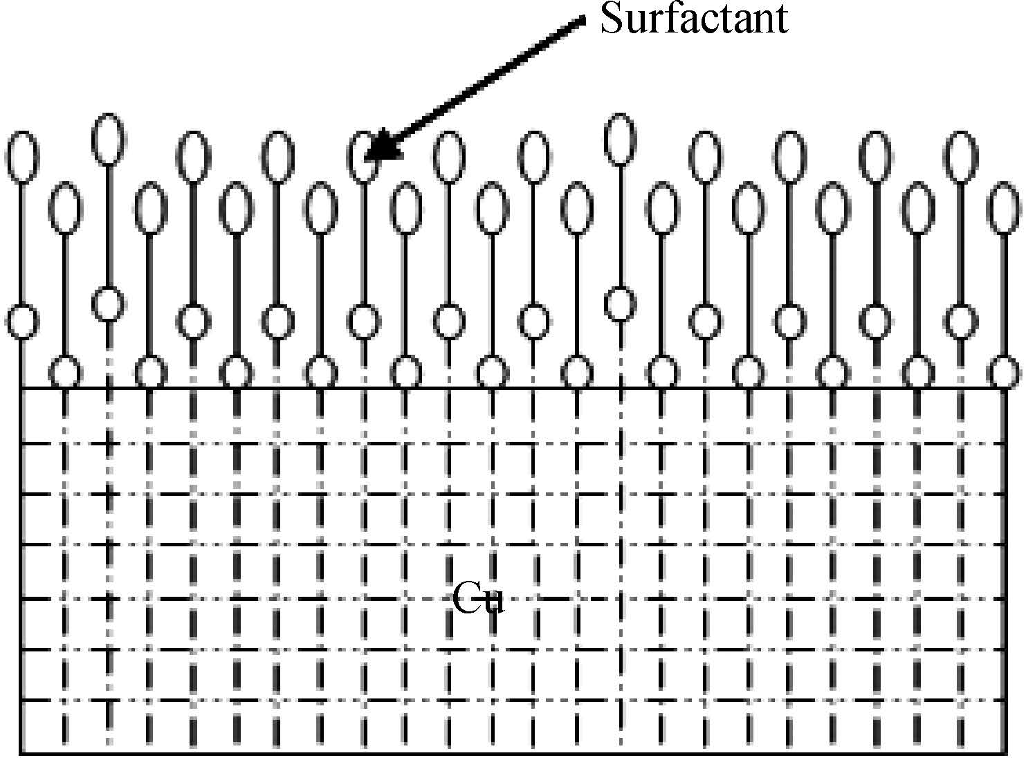

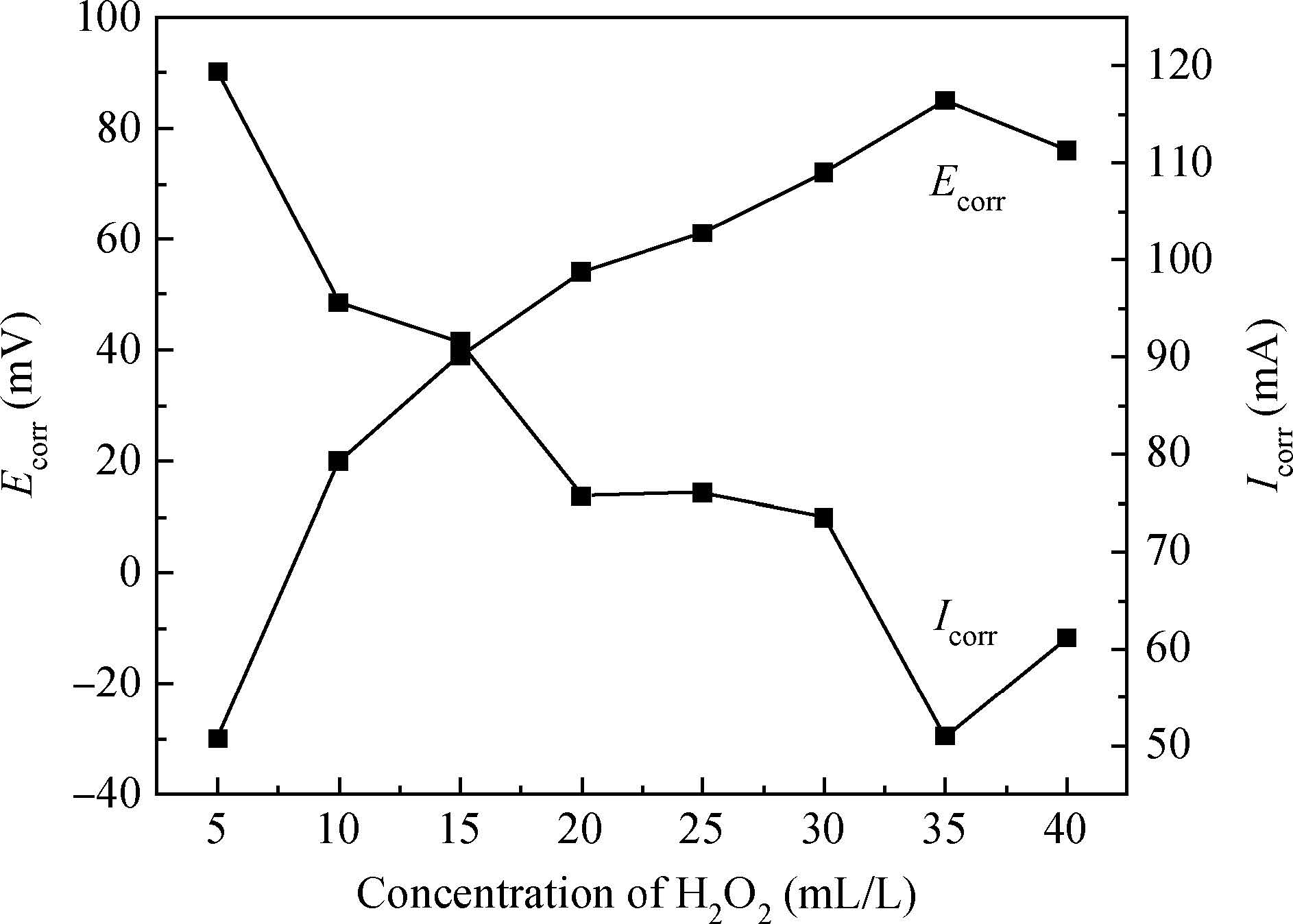
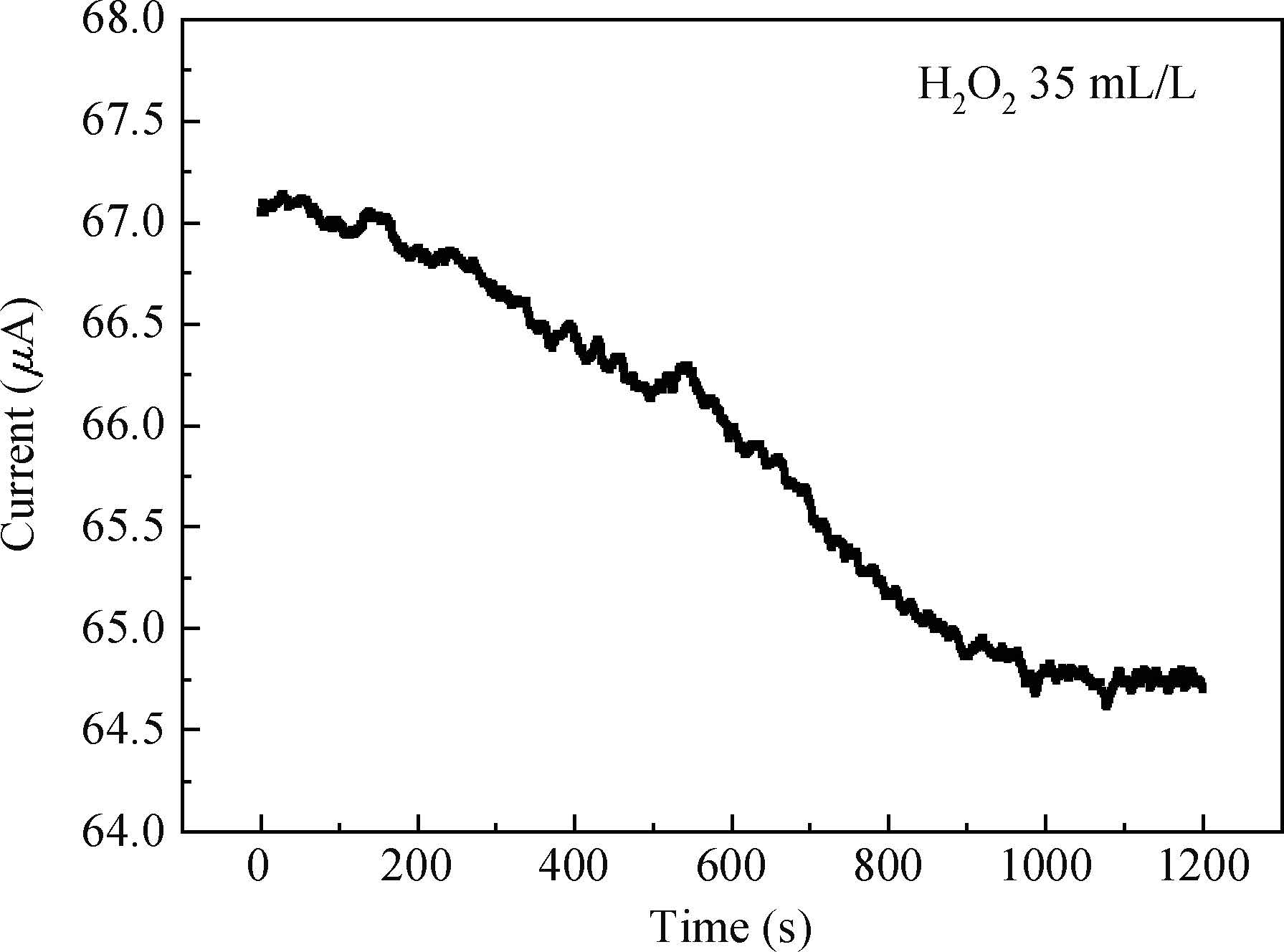
The article studied the electrochemical behavior of P2 alkaline polishing slurry. The main research is the changing discipline of Ecorr and Icorr in the Cu electrolyte at different concentrations of oxidant H2O2. It compares potentiodynamic polarization curves in different P2 slurries and analyzes the passivation function of H2O2 acting on controlling dishing. The result implies that the potential increases gradually and then levels off while the current density on the contrary decreases with the augment of H2O2 concentration. In addition, dishing declines with the increasing of H2O2 along with the optimization of planarization of the alkaline P2 slurry.