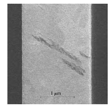
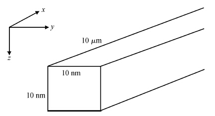
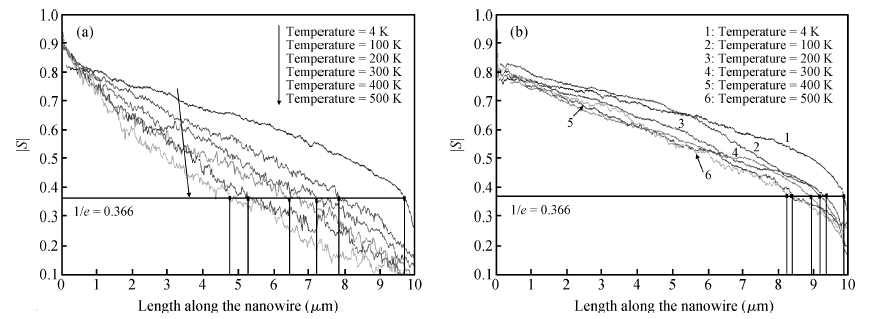
We have analyzed the spin transport behaviour of four II—VI semiconductor nanowires by simulating spin polarized transport using a semi-classical Monte-Carlo approach. The different scattering mechanisms considered are acoustic phonon scattering, surface roughness scattering, polar optical phonon scattering, and spin flip scattering. The II—VI materials used in our study are CdS, CdSe, ZnO and ZnS. The spin transport behaviour is first studied by varying the temperature (4—500 K) at a fixed diameter of 10 nm and also by varying the diameter (8—12 nm) at a fixed temperature of 300 K. For II—VI compounds, the dominant mechanism is for spin relaxation; D'yakonovPerel and Elliot Yafet have been actively employed in the first order model to simulate the spin transport. The dependence of the spin relaxation length (SRL) on the diameter and temperature has been analyzed.


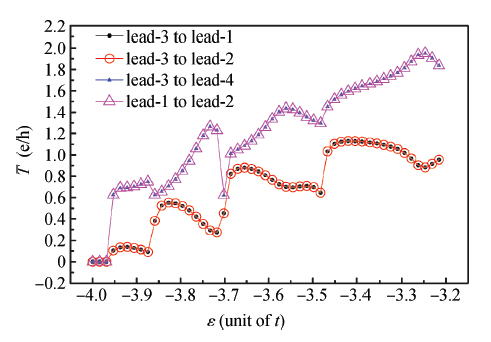
Quantum pump effect in a four-terminal mesoscopic structure constructed from a homogeneous two-dimensional electron gas is investigated. Oscillating electric potentials are applied to the two opposite terminals of the four-terminal mesoscopic structure. In both the remaining two opposite terminals and in the central region there are constant potentials that do not change with time. The oscillating potentials change slowly in comparison with all of the internal time scales of the structure and the amplitude of the oscillating potentials is small in comparison with the Fermi energy. The current of each lead and the transmission coefficients from one lead to another are calculated by using the non-equilibrium Green's function approach under the adiabatic approximation. In the remaining two opposite terminals of the four-terminal structure, the quantum pump effect can produce an electric current whose magnitude and direction depends on the Fermi energy. The pumped currents are ascribed to the asymmetry of transmission coefficients with respect to the Fermi energy.


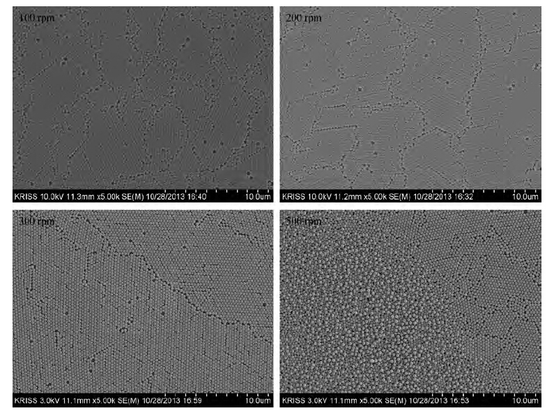
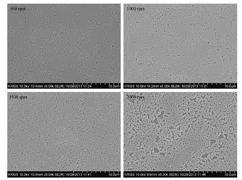
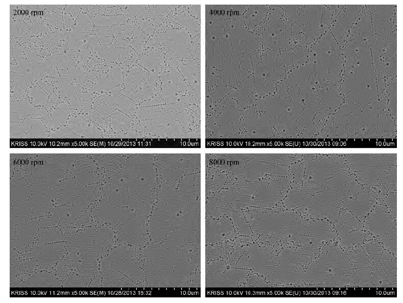
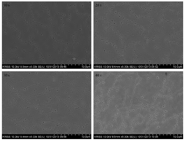
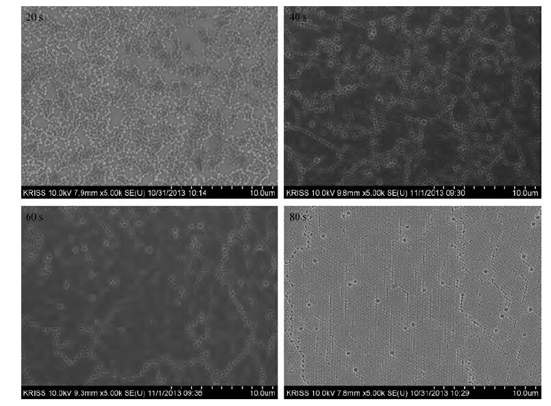
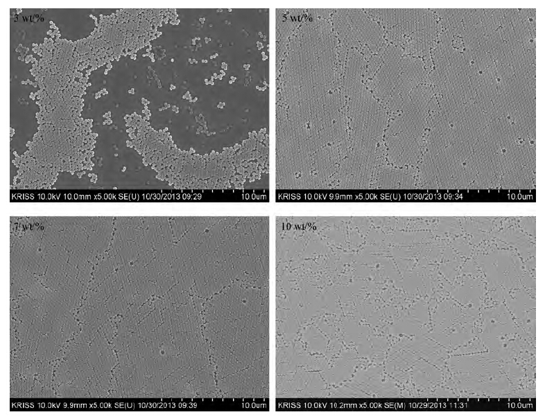
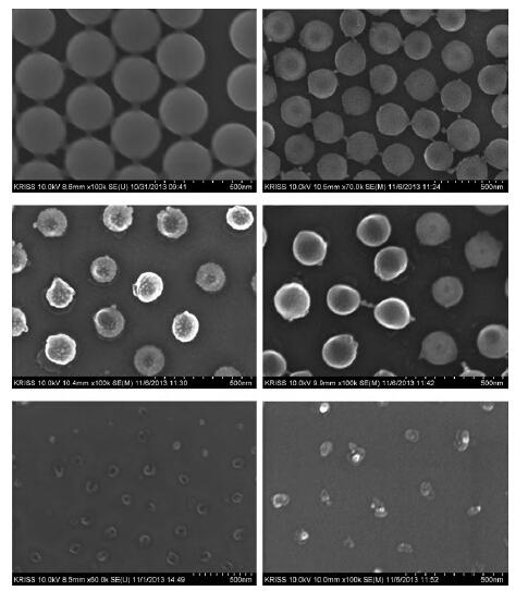
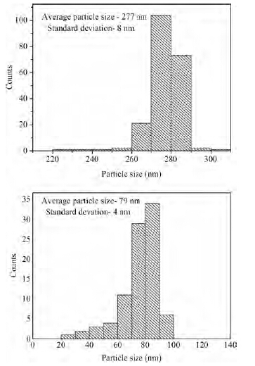
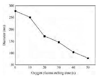
We developed a simple and inexpensive synthesis of a large-scale close-packed monolayer of polystyrene sphere arrays, which have a variety of applications. The influence of three step spin speeds, spinning time, solution quantity and relative humidity is studied in order to achieve a large area close-packed monolayer. A relatively high surface coverage and uniform monolayer of PS spheres in the range of 85%—90% are achieved by appropriate control of the preparative parameters. Also the effect of the oxygen plasma etching process on the reduction of PS spheres has been studied. We conclude that it can be useful in industrial applications, because of the fabrication speed, surface coverage, control over PS spheres and cost of the process.


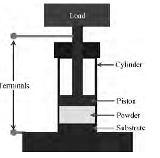
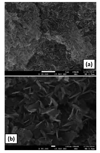
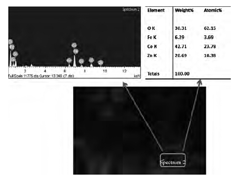
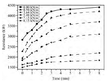
This study presents the synthesis of metal oxides composite nanosheets (oxides of cobalt, zinc and iron) and their pressure sensing properties. A transducer has been fabricated to directly measure the resistance—pressure and impedance—pressure relationships of pristine nanopowder. At the initial stage, a nanopowder sample of 10 mm diameter and 1 mm height was placed in the transducer and by applying pressure of up to 8.15 kN/m2; the DC resistance and the impedance are reduced by 44% on average. It can be explained by the densification of the samples and a decrease in porosity due to the effect of pressure. It was also observed that the DC resistance increases with time and saturated within 8 min. It is considered that this phenomenon is based on the effect of displacement currents of bound charges. The dependences of the impedance phase (θ) on frequency and pressure have also been investigated.


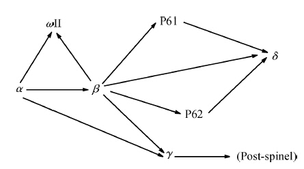
This paper describes the results of structural, electronic and elastic properties of silicon nitride (in its high-pressure P61 and P62 phases) through the first-principles calculation combined with an ultra-soft pseudo-potential. The computed equilibrium lattice constants agree well with the experimental data and the theoretical results. The strongest chemical bond (N--Si bond) shows a covalent nature with a little weaker ionic character. P61-Si3N4 is more stable than P62-Si3N4 due mainly to the fact that the shorter N--Si bond in the P61 phase allows stronger electron hybridizations. We have also predicted the phase stability of Si3N4 using the quasi-harmonic approximation, in which the lattice vibration and phonon effect are both considered. The results show that the β → P61 phase transition is very likely to occur at 42.9 GPa and 300 K. The reason why the β → P61 → δ phase transitions had never been observed is also discussed.

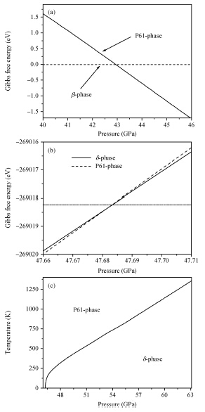

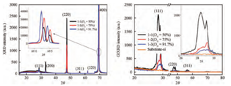
Polycrystalline silicon (poly-Si) films were prepared by hot-wire chemical vapor deposition (HWCVD) at a low substrate temperature of 525 ℃. The influence of hydrogen on the epitaxial growth of ploy-Si films was investigated. Raman spectra show that the poly-Si films are fully crystallized at 525 ℃ with a different hydrogen dilution ratio (50%—91.7%). X-ray diffraction, grazing incidence X-ray diffraction and SEM images show that the poly-Si thin films present (100) preferred orientation on (100) c-Si substrate in the high hydrogen dilution condition. The P-type poly-Si film prepared with a hydrogen dilution ratio of 91.7% shows a hall mobility of 8.78 cm2/(V·s) with a carrier concentration of 1.3 × 1020 cm-3, which indicates that the epitaxial poly-Si film prepared by HWCVD has the possibility to be used in photovoltaic and TFT devices.


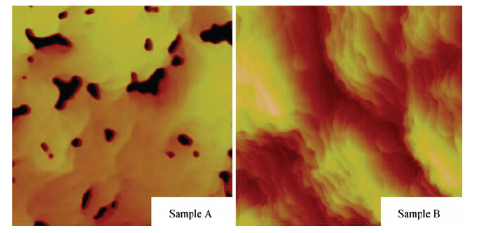
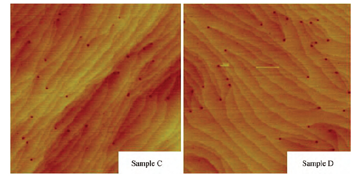
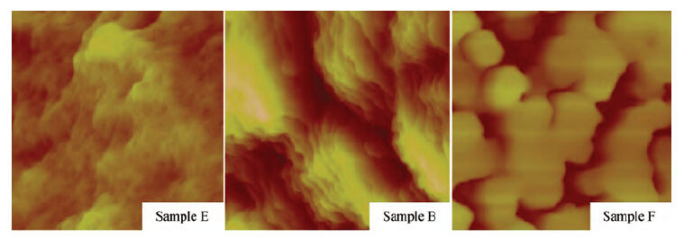
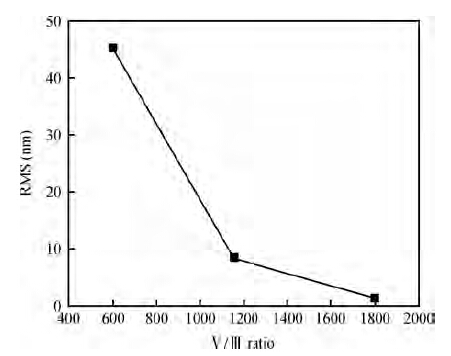
The initial growth conditions of a 100 nm thick GaN layer and Mg-surfactant on the quality of the GaN epilayer grown on a 6H-SiC substrate by metal-organic vapor phase epitaxy have been investigated in this research. Experimental results have shown that a high V/III ratio and the initially low growth rate of the GaN layer are favorable for two-dimension growth and surface morphology of GaN and the formation of a smoother growth surface. Mg-surfactant occurring during GaN growth can reduce the dislocations density of the GaN epilayer but increase the surface RMS, which are attributed to the change of growth mode.

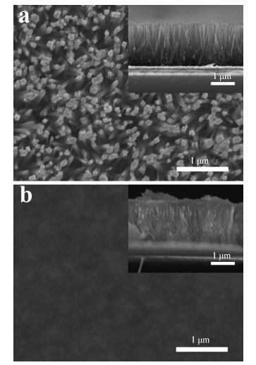
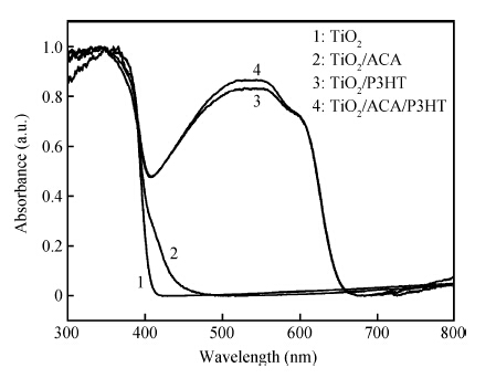
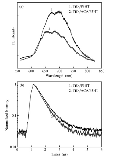
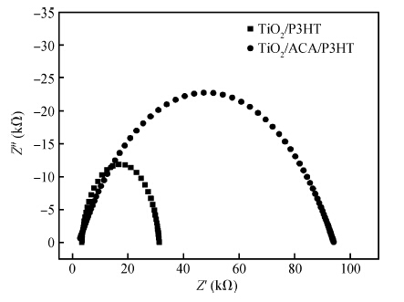
A TiO2/P3HT hybrid solar cell was fabricated by infiltrating P3HT into the pores of TiO2 nanorod arrays. To further enhance the photovoltaic performance, anthracene-9-carboxylic acid was employed to modify the interface of TiO2/P3HT before P3HT was coated. Results revealed that the interface treatment significantly enhances the photovoltaic performance of the cell. The efficiency of the hybrid solar cells reaches 0.28% after interface modification, which is three times higher compared with the un-modified one. We find that except for the increased exciton dissociation efficiency recognized by the previous reports, the suppressing of electron back recombination is another important factor leading to the enhanced photovoltaic performance.


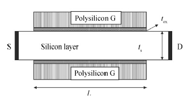
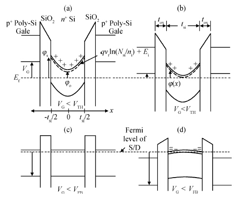
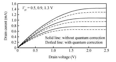
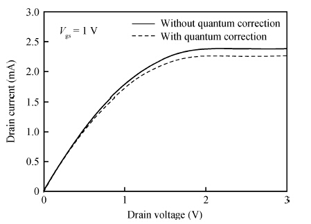
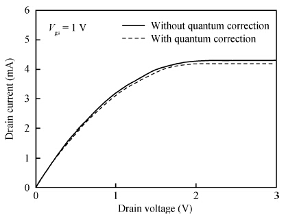
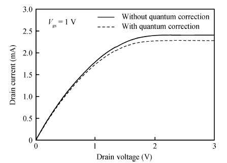
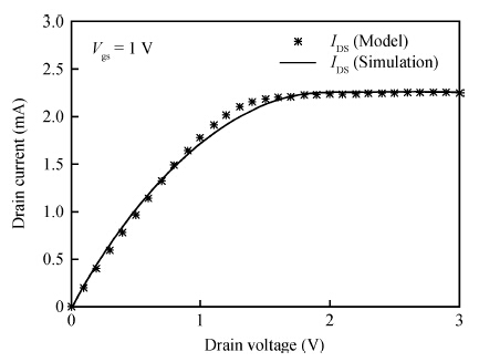
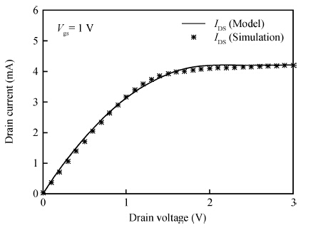
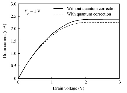
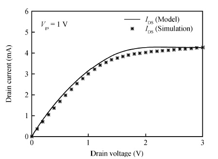
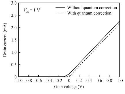
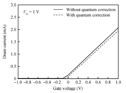
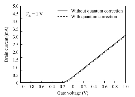
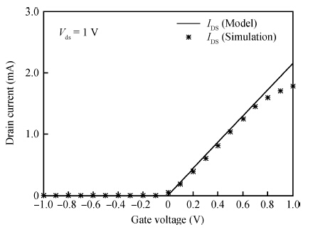
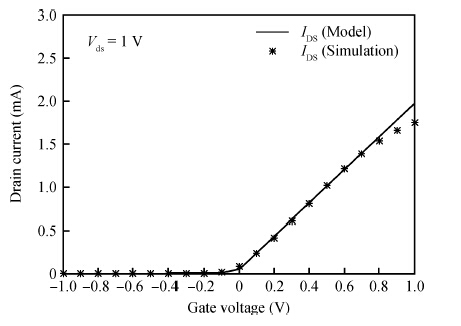
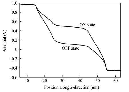
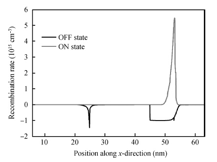
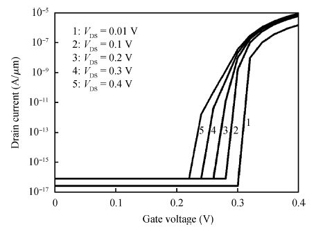
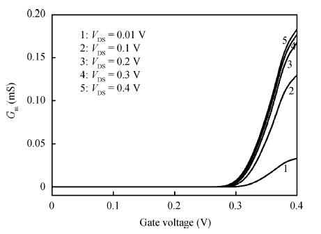
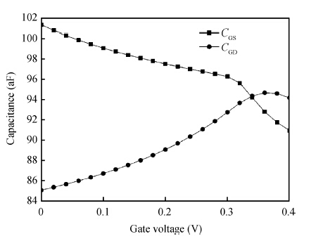
We investigate the quantum-mechanical effects on the electrical properties of the double-gate junction-less field effect transistors. The quantum-mechanical effect, or carrier energy-quantization effects on the threshold voltage, of DG-JLFET are analytically modeled and incorporated in the Duarte et al. model and then verified by TCAD simulation.


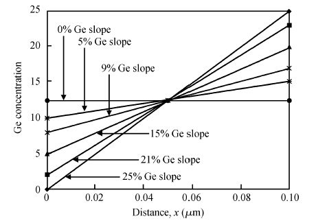
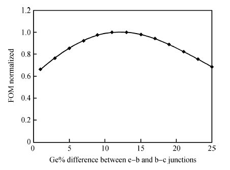
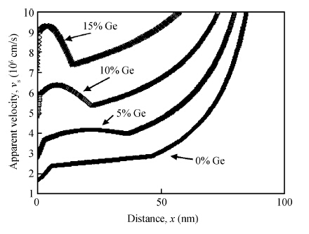
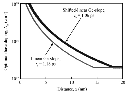
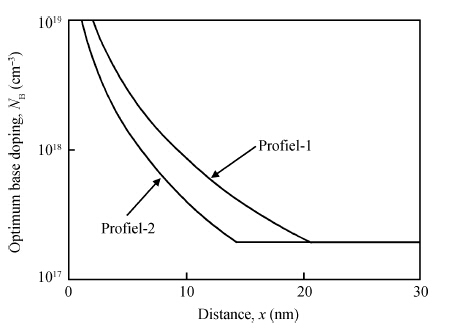
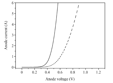
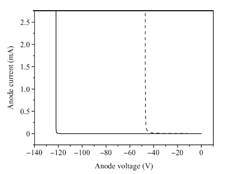
This work presents a unique and robust approach for validation of using the box-triangular germanium profile in the base of SiGe heterojunction bipolar transistors, where the methodology considers the simultaneous optimization of the p-type base doping profile in conjunction with the germanium profile in the base. The study analyses the electron motion across the SiGe base in SiGe HBTs, owing to different accelerating electric fields. The analysis first presents a figure of merit, to achieve the minimum electron transit time across the base in conjunction with the increased current gain in n—p—n-SiGe HBTs, which shows a general trend vis-v-vis the advantage of a trapezoid germanium profile, but with additional accuracy as we considered simultaneously optimized p-type base doping. The effect of minority carrier velocity saturation is then included to make the study more detailed. The analysis then investigates the shifted germanium profile in the base to further minimize the base transit time. Finally, it is shown that a shifted germanium profile eventually evolves into a box-triangular Ge-profile in the SiGe base, which could simultaneously minimize the base transit time and reduce emitter delay by virtue of the high current gain. The analysis verifies that for an average Ge-dose of 7.5% Ge across the base, a box-triangular germanium profile in conjunction with an optimum base doping profile has an approximately identical base transit time and a 30% higher current gain, in comparison with an optimum base doping and triangular Ge-profile across the whole base.


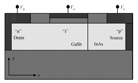
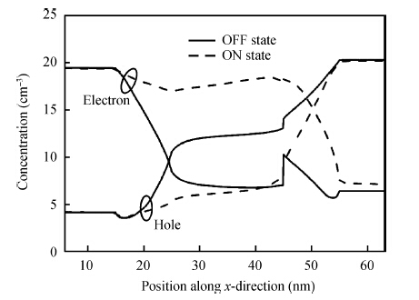
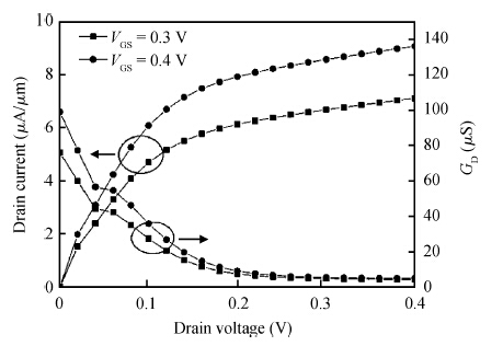
We present a GaSb/InAs junctionless tunnel FET and investigate its static device characteristics. The proposed structure presents tremendous performance at a very low supply voltage of 0.4 V. The key idea is to the present device architecture, which can be exploited as a digital switching device for sub 20 nm technology. Numerical simulations resulted in an IOFF of ~8 × 10-17 A/μm, ION of ~ 9 μA/μm, ION/IOFF of ~1 × 10¹¹, subthreshold slope of 9.33 mV/dec and DIBL of ~ 87 mV/V for GaSb/InAs JLTFET at a temperature of 300 K, gate length of 20 nm, HfO2 gate dielectric thickness of 2 nm, film thickness of 10 nm, low-k spacer thickness of 10 nm and VDD of 0.4 V.


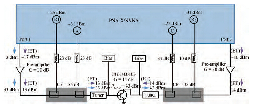
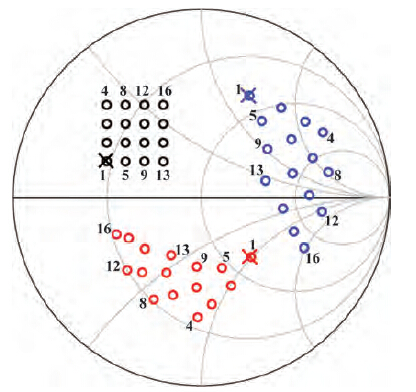
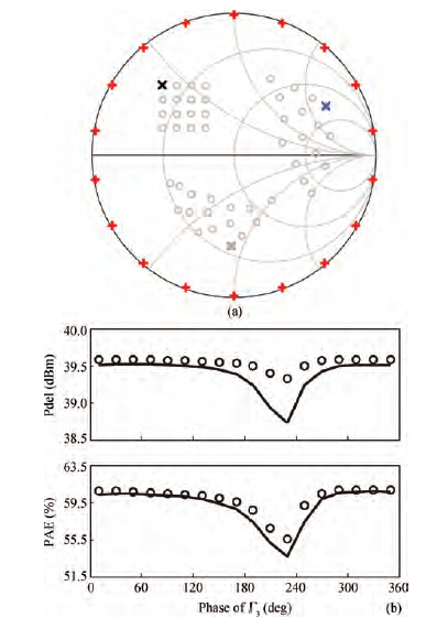
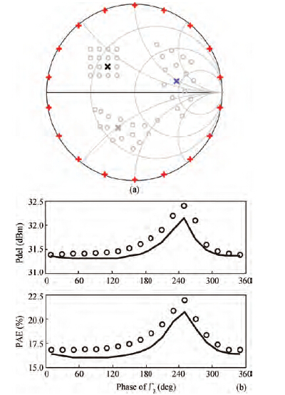
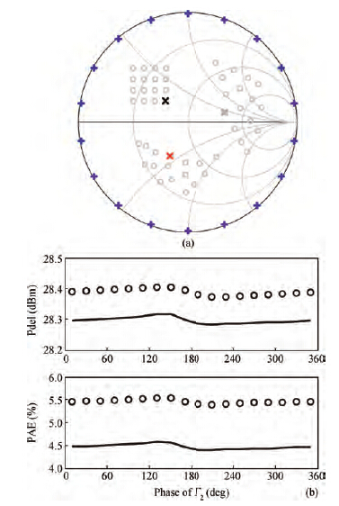
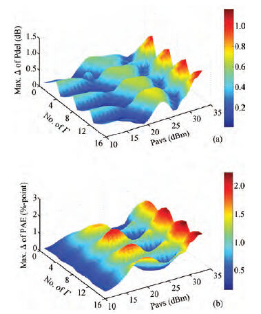
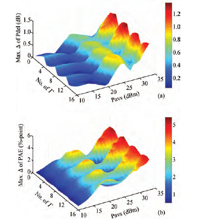
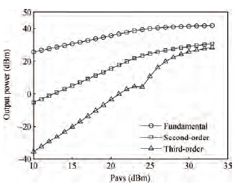
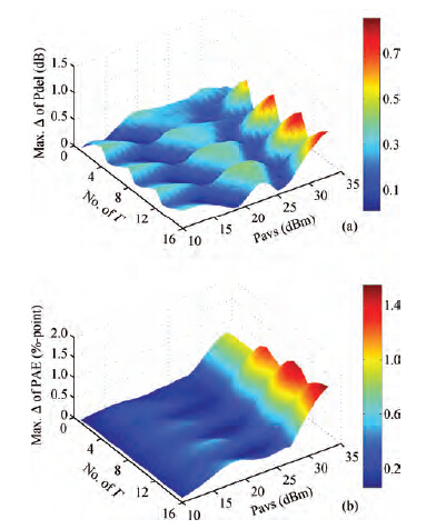
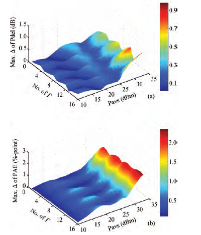
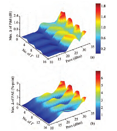
Characterization of power transistors is an indispensable step in the design of radio frequency and microwave power amplifiers. A full harmonic load-pull measurement setup is normally required for the accurate and comprehensive characterization of RF power transistors. The setup is usually highly complex, leading to a relatively high hardware cost and low measurement throughput. This paper presents X-parameter measurement on a gallium nitride (GaN) high-electron-mobility transistor and studies the potential of utilizing an X-parameter-based modeling technique to highly reduce the complexity of the harmonic load-pull measurement setup for transistor characterization. During the X-parameter measurement and characterization, load impedance of the device is tuned and controlled only at the fundamental frequency and is left uncontrolled at other higher harmonics. However, it proves preliminarily that the extracted X-parameters can still predict the behavior of the device with moderate to high accuracy, when the load impedance is tuned up to the third-order harmonic frequency. It means that a fundamental-only load-pull test setup is already enough even though the device is to be characterized under load tuning up to the third-order harmonic frequency, by utilizing X-parameters.


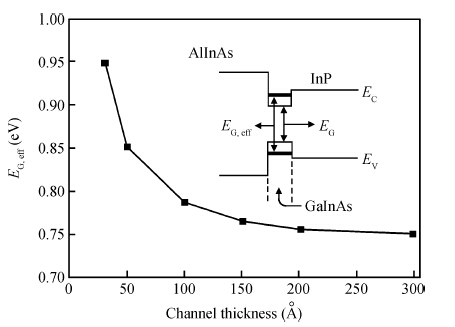
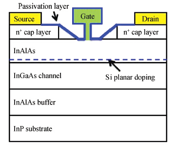
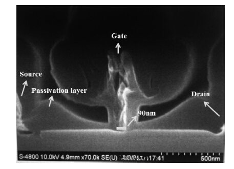
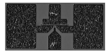
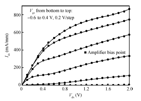
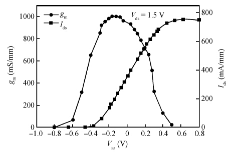
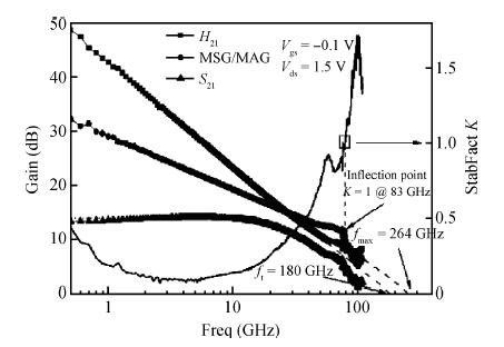
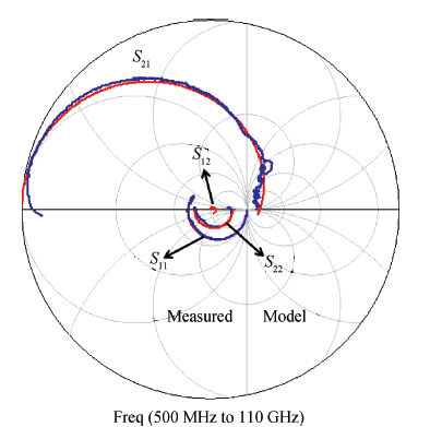
90-nm T-shaped gate InP-based In0.52Al0.48As/In0.6Ga0.4As pseudomorphic high electron mobility transistors were designed and fabricated with a gate-width of 2 × 30 μm, a source—drain space of 2.5 μm, and a source—gate space of 0.75 μm. DC, RF and small-signal model characterizations were demonstrated. The maximum saturation current density was measured to be 755 mA/mm biased at Vgs = 0.6 V and Vds = 1.5 V. The maximum extrinsic transconductance was measured to be 1006 mS/mm biased at Vgs = -0.1 V and Vds = 1.5 V. The extrapolated current gain cutoff frequency and maximum oscillation frequency based on S-parameters measured from 0.5 to 110 GHz were 180 and 264 GHz, respectively. The inflection point (the stability factor k= 1) where the slope from —10 dB/decade (MSG) to —20 dB/decade (MAG) was measured to be 83 GHz. The small-signal model of this device was also established, and the S-parameters of the model are consistent with those measured from 0.5—110 GHz.


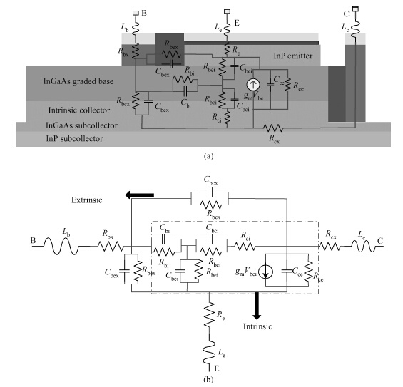
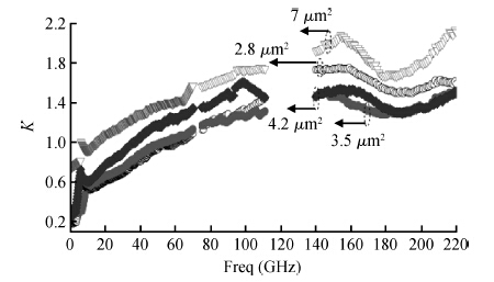
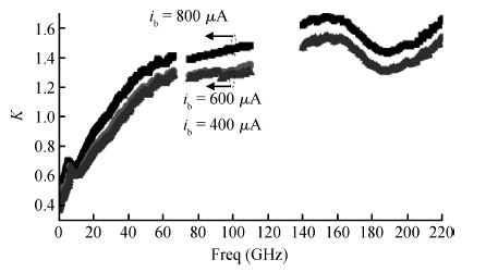
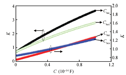
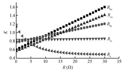
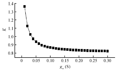
The frequency stabilities of InP DHBTs in a broadband over 1 to 220 GHz are investigated. A hybrid π-topology small-signal model is used to accurately capture the parasitics of devices. The model parameters are extracted from measurements analytically. The investigation results show that the excellent agreement between the measured and simulated data is obtained in the frequency range 200 MHz to 220 GHz. The dominant parameters of the π-topology model, bias conditions and emitter area have significant effects on the stability factor K. The HBT model can be unconditionally stable by reasonable selection of the proper bias condition and the physical layout of the device.


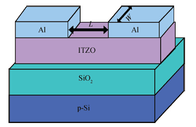
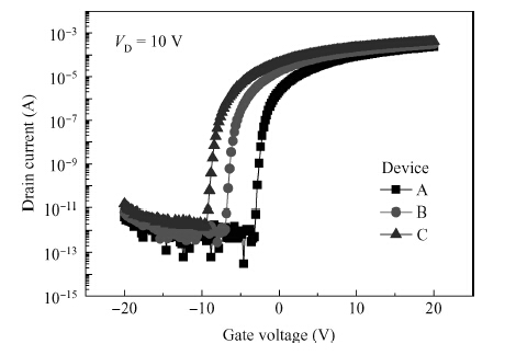
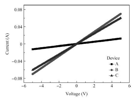
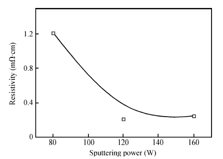
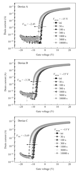
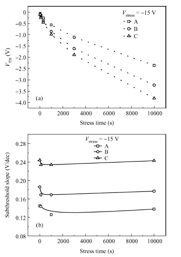
We reported the influence of interface trap density (Nt) on the electrical properties of amorphous InSnZnO based thin-film transistors, which were fabricated at different direct-current (DC) magnetron sputtering powers. The device with the smallest Nt of 5.68 × 1011 cm-2 and low resistivity of 1.21 × 10⁻³ Ω · cm exhibited a turn-on voltage (VON) of -3.60 V, a sub-threshold swing (S.S) of 0.16 V/dec and an on-off ratio (ION/IOFF) of ~ 8 × 10⁸. With increasing Nt, the VON, S.S and ION/IOFF were suppressed to —9.40 V, 0.24 V/dec and 2.59 × 10⁸, respectively. The VTH shift under negative gate bias stress has also been estimated to investigate the electrical stability of the devices. The result showed that the reduction in Nt contributes to an improvement in the electrical properties and stability.


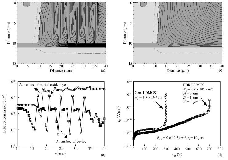
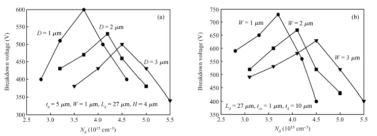
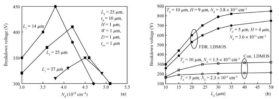
A new high-voltage LDMOS with folded drift region (FDR LDMOS) is proposed. The drift region is folded by introducing the interdigital oxide layer in the Si active layer, the result of which is that the effective length of the drift region is increased significantly. The breakdown characteristic has been improved by the shielding effect of the electric field from the holes accumulated in the surface of the device and the buried oxide layer. The numerical results indicate that the breakdown voltage of 700 V is obtained in the proposed device in comparison to 300 V of conventional LDMOS, while maintaining low on-resistance.


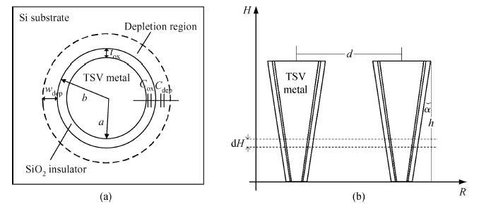
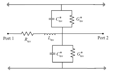
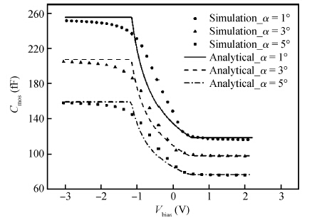
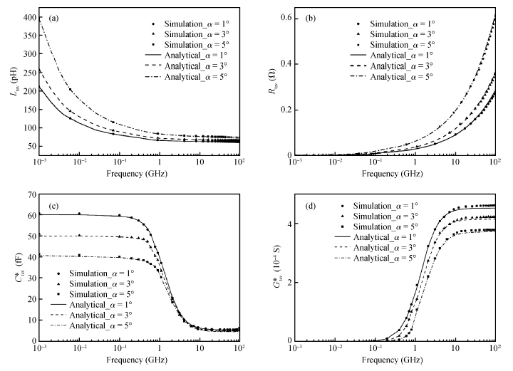
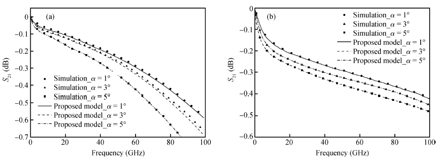
The analytical model of voltage-controlled MOS capacitance of tapered through silicon via (TSV) is derived. To capture the frequency-dependent behavior of tapered TSV, the conventional analytical equations of RLCG for two-wire transmission lines are revised. With the adoption of MOS capacitance model and the revised RLCG analytical equations, a transmission line-type electrical model for tapered TSV is proposed finally. All the proposed models are validated by simulation tools, and a good correlation is obtained between the proposed models and simulations up to 100 GHz. With the proposed model, both the semiconductor phenomenon and frequency-dependent behavior of tapered TSV can be fully captured at high frequency, and the performance of tapered TSV can be evaluated accurately and conveniently prior to 3D IC design.


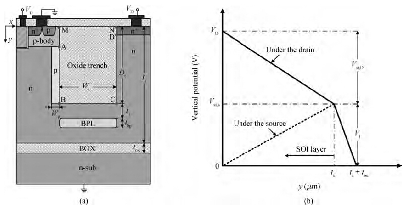
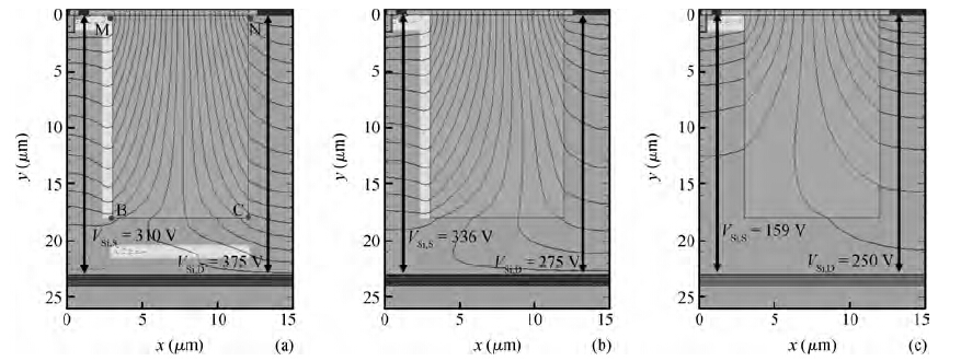
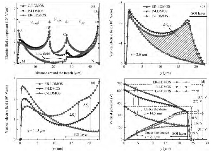
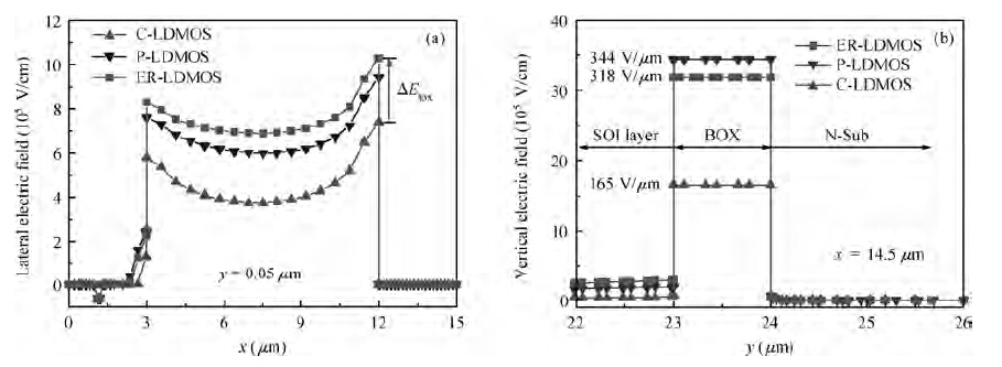
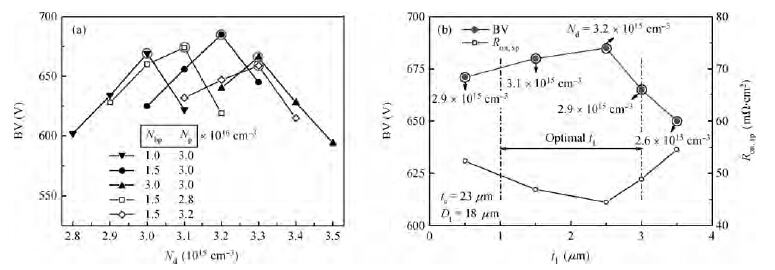
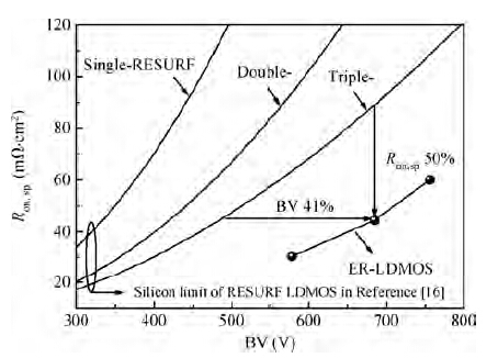
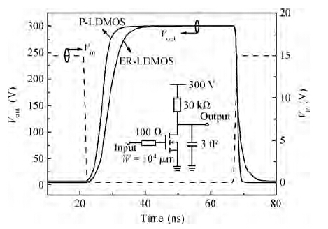
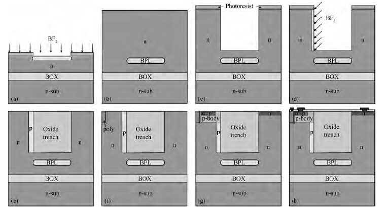
A RESURF-enhanced high voltage SOI LDMOS (ER-LDMOS) with an ultralow specific on-resistance (Ron,sp) is proposed. The device features an oxide trench in the drift region, a P-pillar at the sidewall of the trench, and a buried P-layer (BPL) under the trench. First, the P-pillar adjacent to the P-body not only acts as a vertical junction termination extension (JTE), but also forms a vertical reduced surface field (RESURF) structure with the N-drift region. Both of them optimize the bulk electric field distributions and increase the doping concentration of the drift region. Second, the BPL together with the N-drift region and the buried oxide layer (BOX) exhibits a triple-RESURF effect, which further improves the bulk field distributions and the doping concentration. Additionally, multiple-directional depletion is induced owing to the P-pillar, the BPL, and two MIS-like structures consisting of the N-drift region combined with the oxide trench and the BOX. As a result, a significantly enhanced-RESURF effect is achieved, leading to a high breakdown voltage (BV) and a low Ron,sp. Moreover, the oxide trench folds the drift region in the vertical direction, resulting in a reduced cell pitch and thus Ron,sp. Simulated results show that the ER-LDMOS improves BV by 67% and reduces Ron,sp by 91% compared with the conventional trench LDMOS at the same cell pitch.


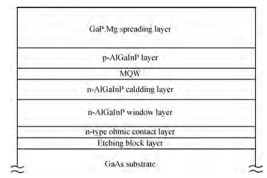
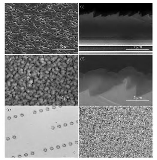
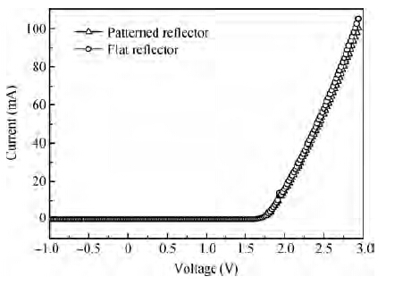
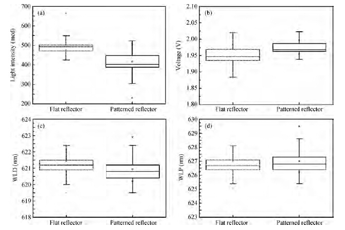
We demonstrate and introduce here a pyramidally patterned metal reflector into wafer-bonding AlGaInP light emitting diodes (LEDs) to improve the light extraction efficiency by using a photo-assisted chemical etched GaP:Mg layer. The pyramid patterns were fabricated employing a HF and H2O2 mixed solution in combination with a 532 nm laser on a GaP:Mg surface firstly, and then a gold reflector layer was evaporated onto the patterned GaP:Mg surface. After the whole chip process, the patterned gold reflector structure was confirmed to be efficient for light extraction and a 18.55% enhancement of the electroluminescent flux has been obtained by an integrating sphere, compared to the surface textured LEDs with flat reflectors.


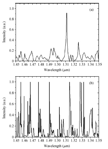
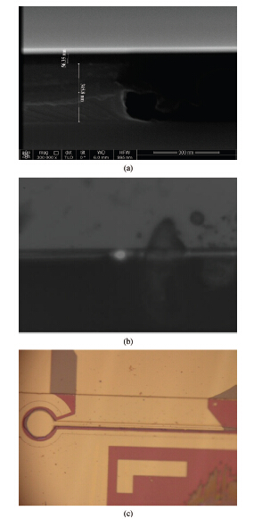
A novel hybrid III—V/silicon deformed micro-disk single-mode laser connecting to a Si output waveguide is designed, and fabricated through BCB bonding technology and standard i-line photolithography. Compared to a traditional circular micro-disk in multi-longitudinal-mode operation, unidirectional emission and single longitudinal-mode output from a Si waveguide are realized. In the experiments, an output power of 0.31 mW and a side-mode suppression ratio of 27 dB in the continuous-wave regime are obtained.

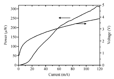


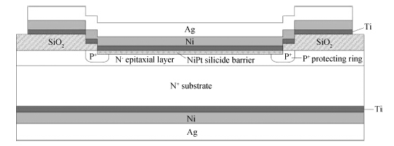
In order to improve the reverse voltage capacity and low junction temperature characteristics of the traditional silicon-based Schottky diode, a Schottky diode with high reverse voltage capacity and high junction temperature was fabricated using ion implantation, NiPt60 sputtering, silicide-forming and other major technologies on an N-type silicon epitaxial layer of 10.6—11.4 μm and (2.2—2.4) × 1015 cm-3 doping concentration. The measurement results show that the junction temperature of the Schottky diode fabricated can reach 175 ℃, that is 50 ℃ higher than that of the traditional one; the reverse voltage capacity VR can reach 112 V, that is 80 V higher than that of the traditional one; the leakage current is only 2 μ A and the forward conduction voltage drop is VF = 0.71 V at forward current IF = 3 A.

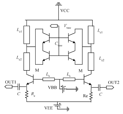
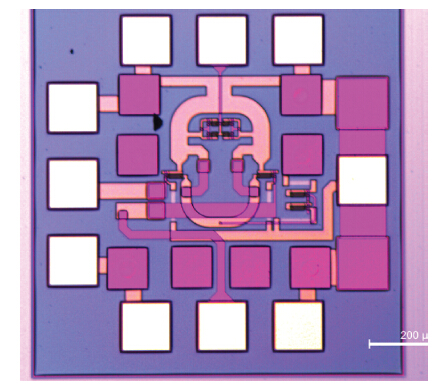
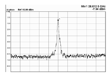
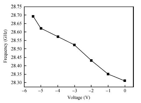
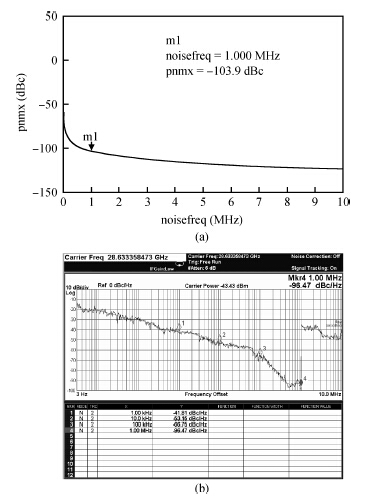
Design and fabrication of a Ka-band voltage-controlled oscillator (VCO) using commercially available 1-μm GaAs heterojunction bipolar transistor technology is presented. A fully differential common-emitter configuration with a symmetric capacitance with a symmetric inductance tank structure is employed to reduce the phase noise of the VCO, and a novel π-feedback network is applied to compensate for the 180° phase shift. The on-wafer test shows that the VCO exhibits a phase noise of —96.47 dBc/Hz at a 1 MHz offset and presents a tuning range from 28.312 to 28.695 GHz. The overall dc current consumption of the VCO is 18 mA with a supply voltage of -6 V. The chip area of the VCO is 0.7 × 0.7 mm2.

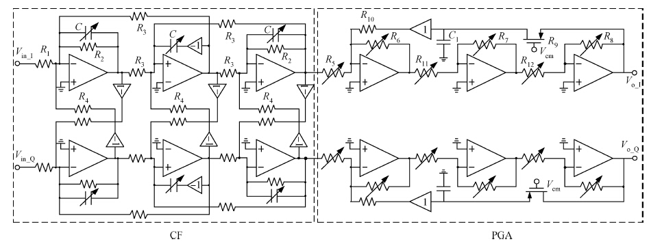
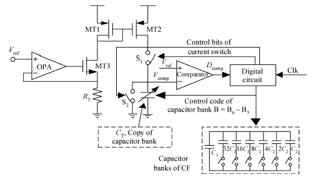
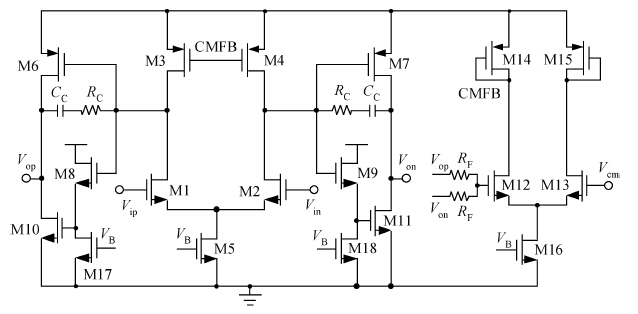
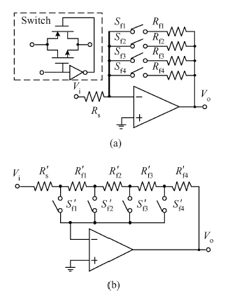
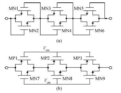
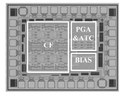
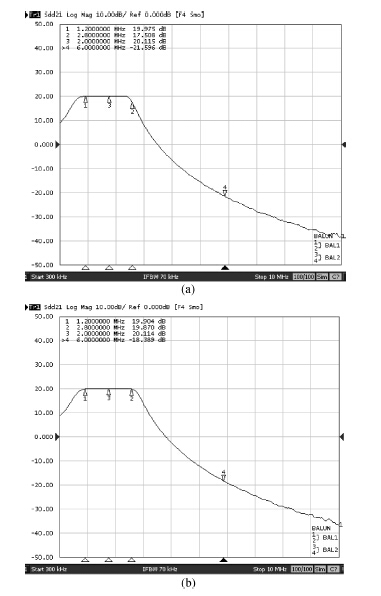
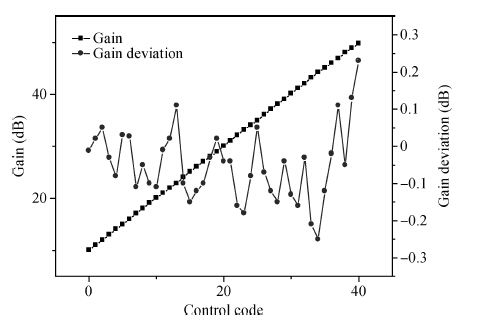
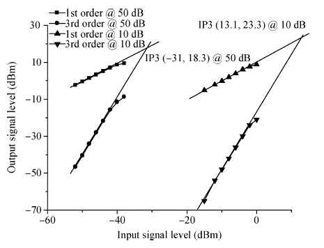
An analog baseband circuit of high linearity and high gain accuracy for a digital audio broadcasting receiver is implemented in a 0.18-μm RFCMOS process. The circuit comprises a 3rd-order active-RC complex filter (CF) and a programmable gain amplifier (PGA). An automatic tuning circuit is also designed to tune the CF's pass band. Instead of the class-A fully differential operational amplifier (FDOPA) adopted in the conventional CF and PGA design, a class-AB FDOPA is specially employed in this circuit to achieve a higher linearity and gain accuracy for its large current swing capability with lower static current consumption. In the PGA circuit, a novel DC offset cancellation technique based on the MOS resistor is introduced to reduce the settling time significantly. A reformative switching network is proposed, which can eliminate the switch resistor's influence on the gain accuracy of the PGA.The measurement result shows the gain range of the circuit is 10—50 dB with a 1-dB step size, and the gain accuracy is less than ± 0.3 dB. The OIP3 is 23.3 dBm at the gain of 10 dB. Simulation results show that the settling time is reduced from 100 to 1 ms. The image band rejection is about 40 dB. It only draws 4.5 mA current from a 1.8 V supply voltage.


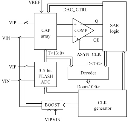
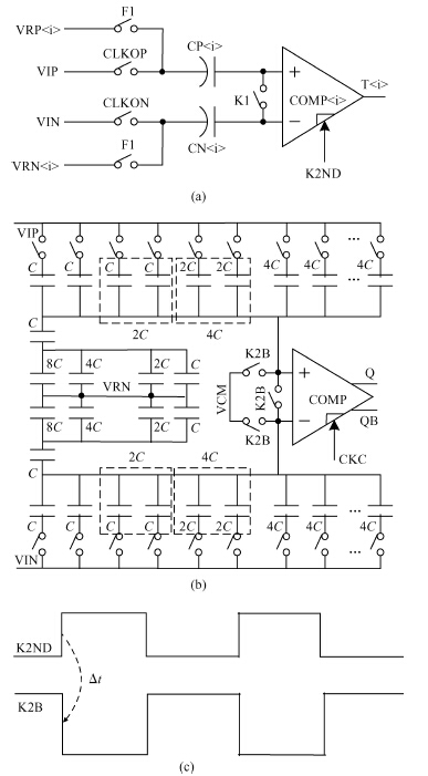
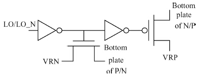
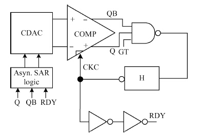
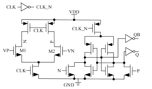
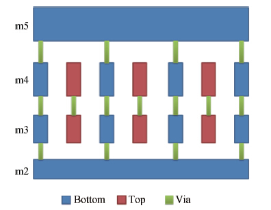
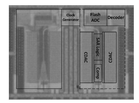
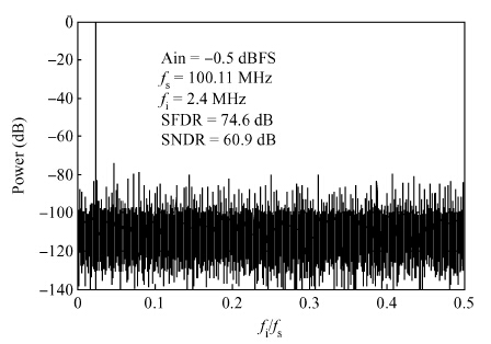
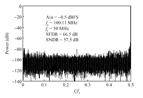
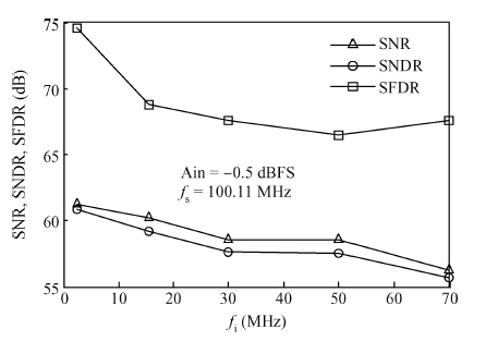
This paper presents a dual-channel 11-bit 100 MS/s hybrid SAR ADC IP. Each channel adopts flash-SAR architecture for high speed, low power and high linearity. Dynamic comparators in the coarse flash ADC and the fine SAR ADC further contribute to the reduction of power consumption. A gate-controlled ring oscillator generates a multi-phase clock for SAR logic, thereby allowing it to asynchronously trigger the comparator in the fine SAR ADC in high speed. MOM capacitors with a fully shielded structure provide enough matching accuracy without the need for calibration. This design was fabricated in SMIC 55 nm low leakage CMOS technology and the active area of dual-channel (I-Q) ADC is 0.35 mm2, while the core area is 0.046 mm2. It consumes 2.92 mA at a 1.2 V supply, for dual-channel too. The effective number of bits (ENOB) is 9.90 bits at 2.4 MHz input frequency, and 9.34 bits at 50 MHz, leading to a FOM of 18.3 fJ/conversion-step.


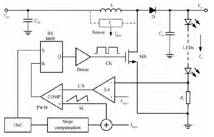
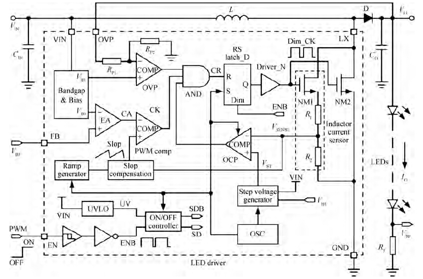
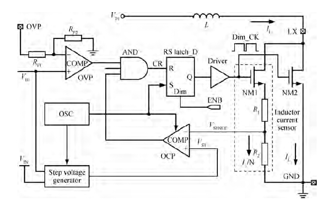
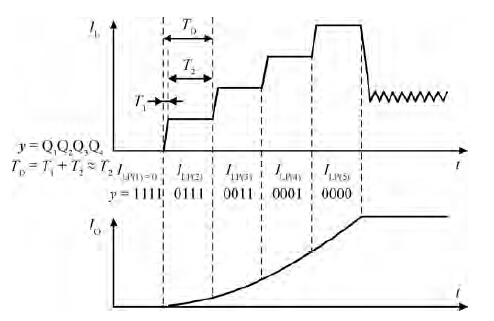
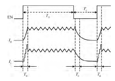
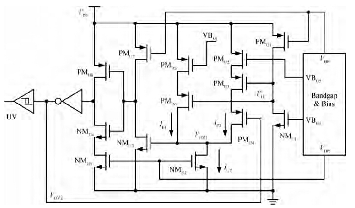
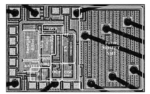
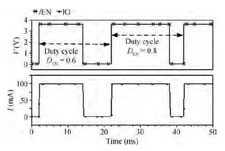
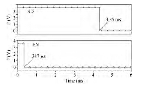
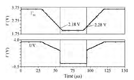
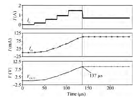
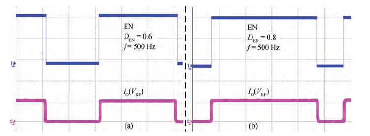
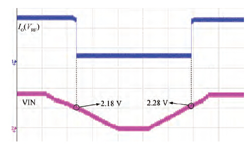
A fully integrated LED driver based on a current mode PWM boost DC—DC converter with constant output current is proposed. In order to suppress the inrush of current and the overshoot voltage at the start up state, a soft-start circuit is adopted. Additionally, to adjust the LED brightness without color variation over the full dimming range and achieve high efficiency, a PWM dimming circuit is presented. Furthermore, to keep the loop stability of the LED driver, an internal slope compensation network is designed to avoid the sub-harmonic oscillation when the duty cycle exceeds 50%. Finally, a UVLO circuit is adopted to improve the reliability of the LED driver against the input voltage changing. The LED driver has been fabricated with a standard 0.5 μm CMOS process, and only occupies 1.21 × 0.76 mm2. Experimental results show that the brightness of the LED can be adjusted by an off-chip PWM signal with a wide adjusting range. The inductor current and output current increase smoothly over the whole load range. The chip is in the UVLO condition when the input voltage is below 2.18 V and has achieved about 137 μs typical start-up time.


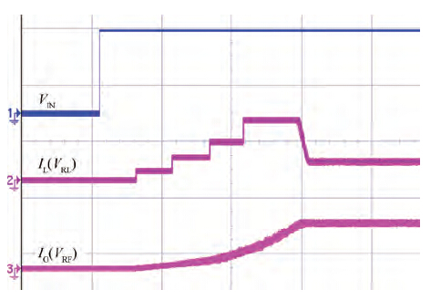

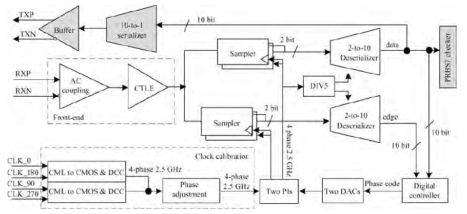
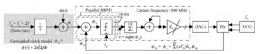
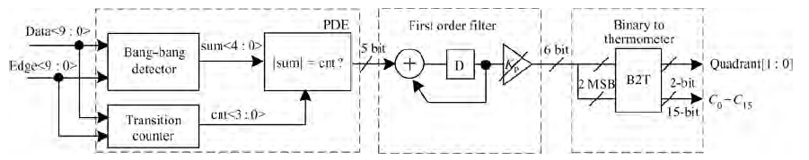
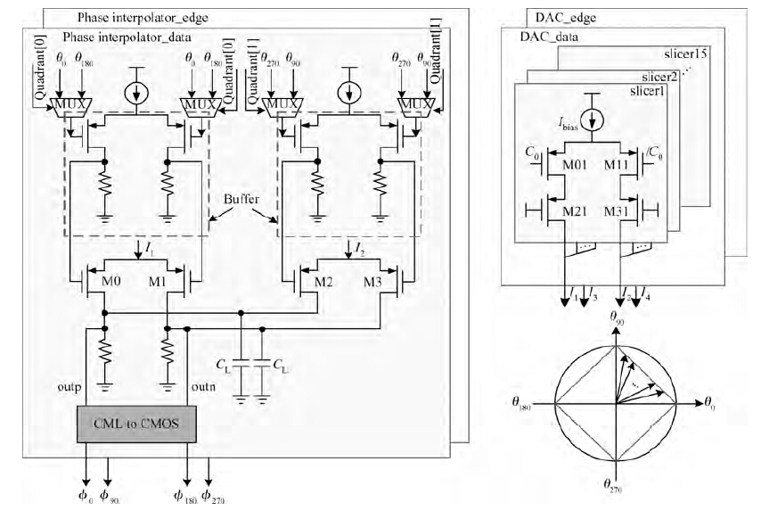
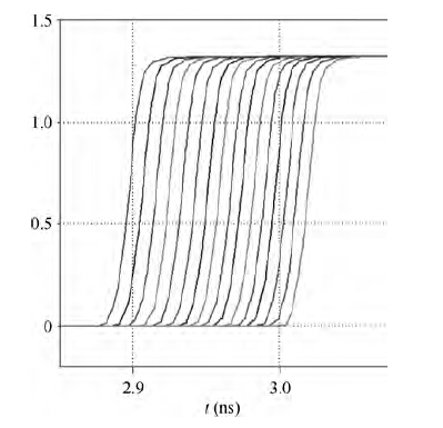
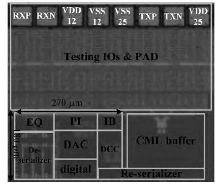
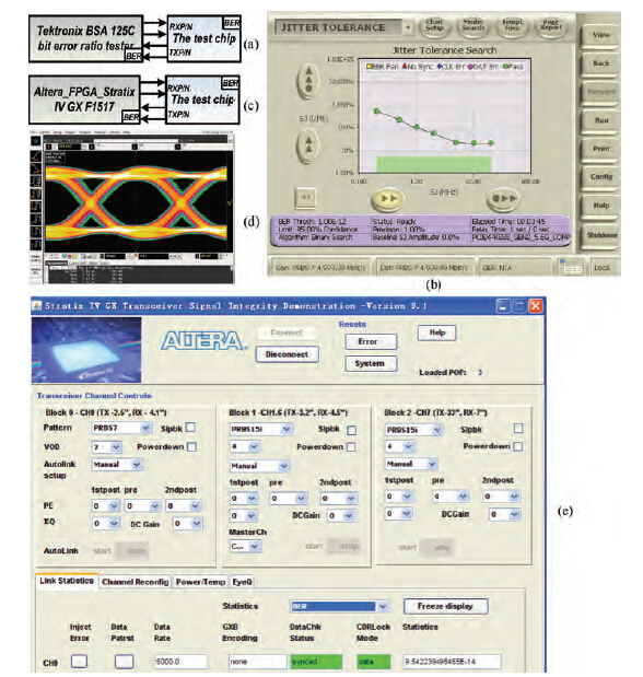
A multi-standard compatible clock and data recovery circuit (CDR) with a programmable equalizer and wide tracking range is presented. Considering the jitter performance, tracking range and chip area, the CDR employs a first-order digital loop filter, two 6-bit DACs and high linearity phase interpolators to achieve high phase resolution and low area. Meanwhile the tracking range is greater than ± 2200 ppm, making this proposed CDR suitable for the embedded clock serial links. A test chip was fabricated in the 55 nm CMOS process. The measurements show that the test chip can achieve BER <10-12 and meet the jitter tolerance specification. The test chip occupies 0.19 mm2 with a 0.0486 mm2 CDR core, which only consumes 30 mW from a 1.2 V supply at 5 Gb/s.


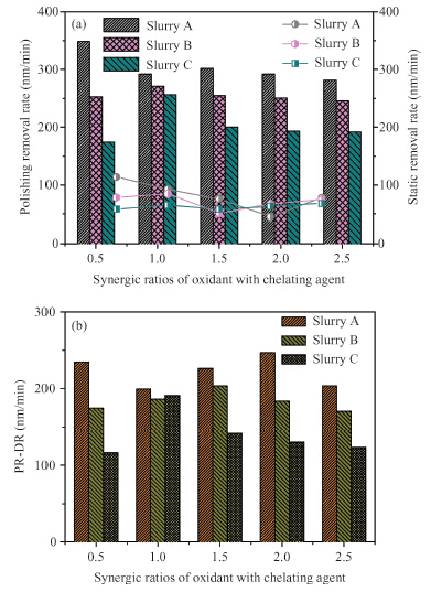
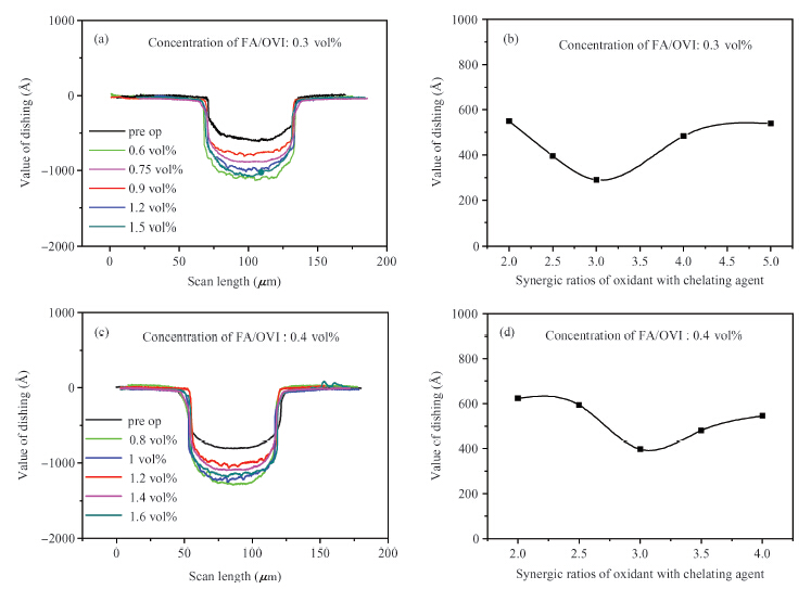
Chemically dominant alkaline slurry, which is free of BTA (benzotriazole) and other inhibitors, was investigated. The synergic effect of the chelating agent and oxidant on the chemical mechanical planarization (CMP) was taken into consideration. Copper CMP slurry is mainly composed of an oxidizer, nonionic surfactant, chelating agent and abrasive particles. The effect of different synergic ratios of oxidant with chelating agent on the polishing removal rate, static etch rate and planarization were detected. The planarization results reveal that with the increase of oxidant concentration, the dishing value firstly diminished and then increased again. When the synergic ratios is 3, the dishing increases the least. A theoretical model combined with chemical-mechanical kinetics process was proposed in the investigation, which can explain this phenomenon. Based on the theoretical model, the effect of synergic ratios of oxidant with chelating agent on velocity D-value (convex removal rate minus recessed removal rate) was analyzed. The results illustrate that when the synergic ratio is between 2.5—3.5, the velocity D-value is relatively higher, thereby good planarization can be achieved in this interval. This investigation provides a new guide to analyze and study copper line corrosion in the recessed region during copper clearing polishing.


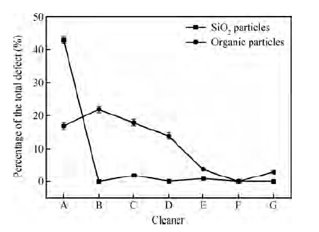
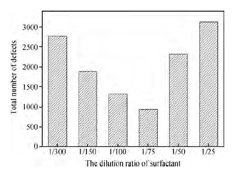
The effect of a non-ionic surfactant on particles removal in post-CMP cleaning was investigated. By changing the concentration of the non-ionic surfactant, a series of experiments were performed on the 12 inch Cu pattern wafers in order to determine the best cleaning results. Then the effect of the surfactant on the reduction of defects and the removal of particles was discussed in this paper. What is more, the negative effect of a non-ionic surfactant was also discussed. Based on the experiment results, it is concluded that the non-ionic surfactant could cause good and ill effects at different concentrations in the post-CMP cleaning process. This understanding will serve as a guide to how much surfactant should be added in order to achieve excellent cleaning performance.