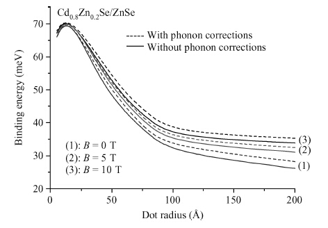
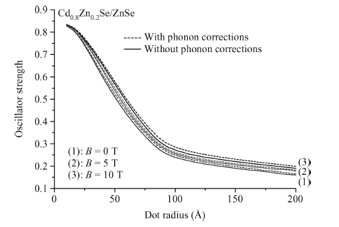
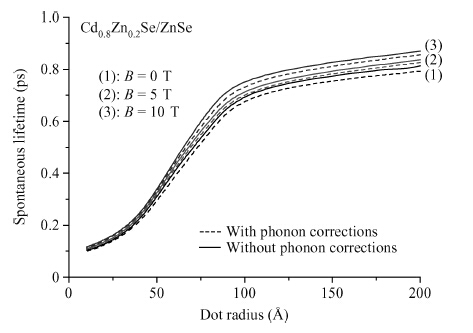
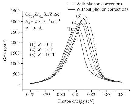
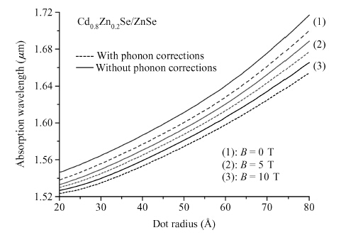
Effects of LO-phonon contribution on the electronic and the optical properties are investigated in a Cd0.8Zn0.2Se/ZnSe quantum dot in the presence of magnetic field strength. The magneto-polaron induced hydrogenic binding energy as a function of dot radius in the wide band gap quantum dot is calculated. The oscillator strength and the spontaneous lifetime are studied taking into account the spatial confinement, magnetic field strength and the phonon contribution. Numerical calculations are carried out using variational formulism within the single band effective mass approximation. The optical properties are computed with the compact density matrix method. The magneto-polaron induced optical gain as a function of photon energy is observed. The results show that the optical telecommunication wavelength in the fiber optic communications can be achieved using CdSe/ZnSe semiconductors and it can be tuned with the proper applications of external perturbations.

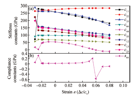
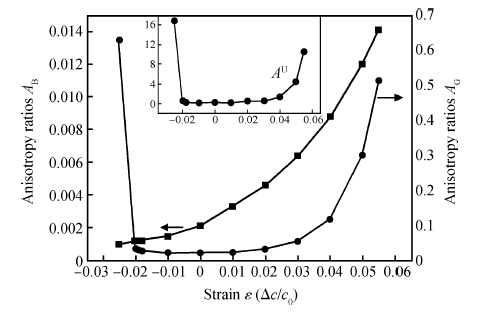
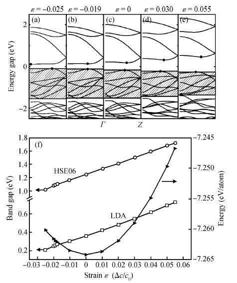
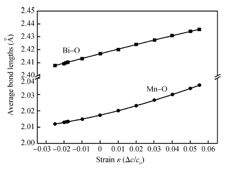
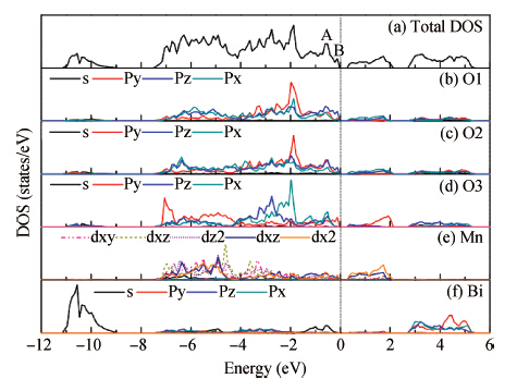
We study the elastic constants and electronic properties of orthorhombic BiMnO3 under uniaxial strain along the c-axis using the first-principles method. It is found that, beyond the range —0.025 < ε <0.055, the predicted stiffness constants cij cannot demand the Born stability criteria and the compliance constant s44 shows abrupt changes, which accompany phase transition. In addition, the results for magnetism moments and polycrystalline properties are also reported. Additionally, under compressive strain, a band gap transition from the indirect to the direct occurs within -0.019 < ε < -0.018. Furthermore, the response of the band gap of orthorhombic BiMnO3 to uniaxial strain is studied.

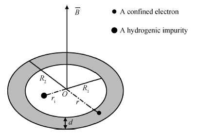
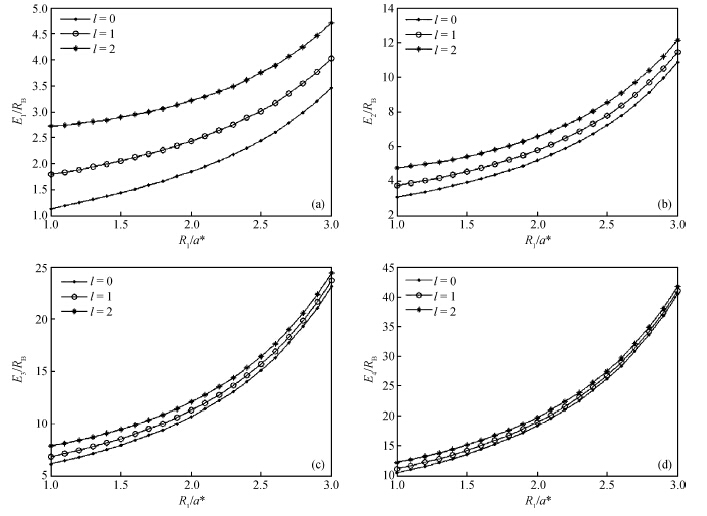
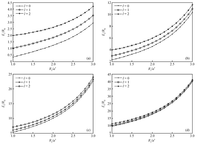
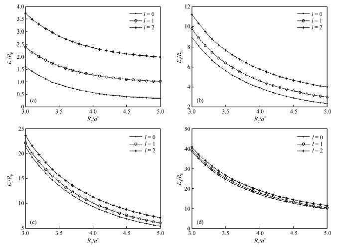
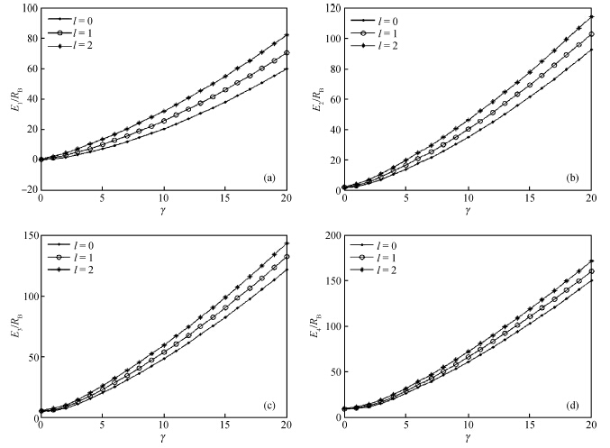
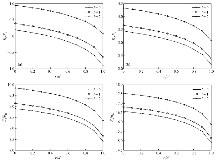
Using the finite element method, we investigate the lowest and first few excited state energies in a two-dimensional GaAs quantum ring (QR) with a hydrogenic donor impurity and effective mass approximation under a uniform magnetic field perpendicular to the ring plane. We study in detail the dependence of the energy spectrum with different angular momentum on the inner radius, the outer radius and width of the QR, the magnetic field and impurity position. The results reveal that the electron energies increase with the inner radius while decrease with the outer radius and width of the QR; for a fixed ring, the magnetic field induces the increase of the electron energies. Moreover, the existence of impurity reduces energy levels, and the energy levels depend highly on the impurity position, which decreases as the impurity is far away from the center of the QR. Also, the dependence of the angular momentum on the energy spectrum is analyzed in detail.


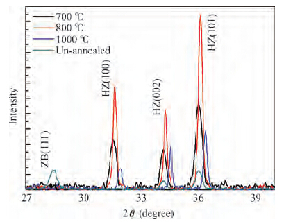
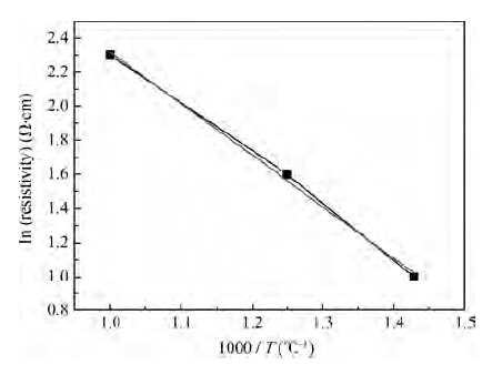
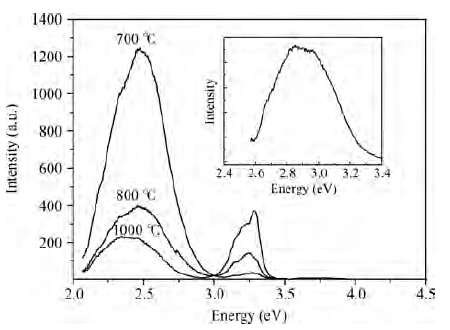
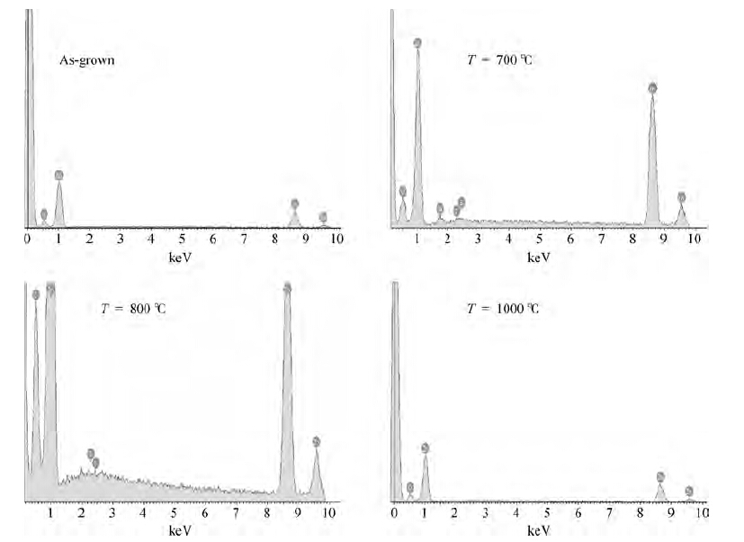
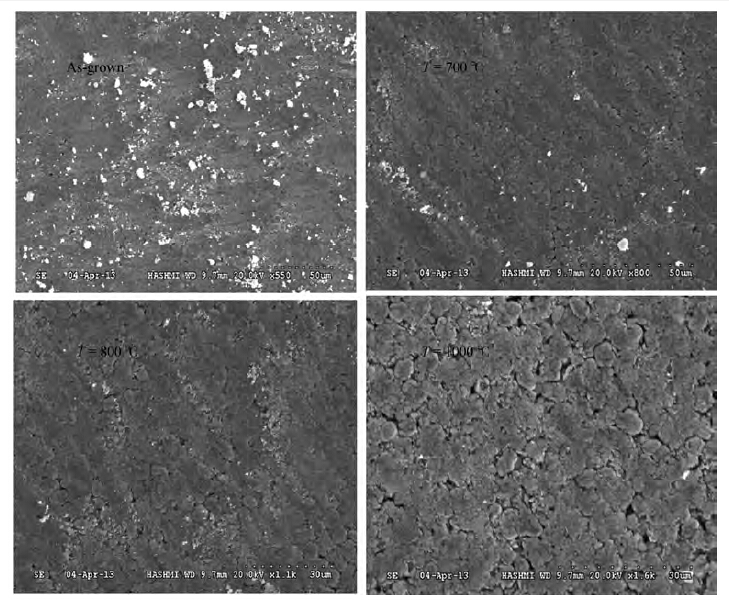
We have investigated the mechanism of phase transformation from ZnS to hexagonal ZnO by high-temperature thermal annealing. The ZnS thin films were grown on Si (001) substrate by thermal evaporation system using ZnS powder as source material. The grown films were annealed at different temperatures and characterized by X-ray diffraction (XRD), photoluminescence (PL), four-point probe, scanning electron microscope (SEM) and energy dispersive X-ray diffraction (EDX). The results demonstrated that as-deposited ZnS film has mixed phases but high-temperature annealing leads to transition from ZnS to ZnO. The observed result can be explained as a two-step process: (1) high-energy O atoms replaced S atoms in lattice during annealing process, and (2) S atoms diffused into substrate and/or diffused out of the sample. The dissociation energy of ZnS calculated from the Arrhenius plot of 1000/T versus log (resistivity) was found to be 3.1 eV. PL spectra of as-grown sample exhibits a characteristic green emission at 2.4 eV of ZnS but annealed samples consist of band-to-band and defect emission of ZnO at 3.29 eV and 2.5 eV respectively. SEM and EDX measurements were additionally performed to strengthen the argument.

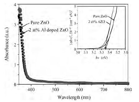
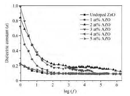
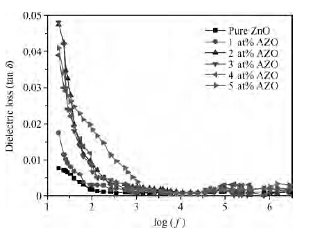
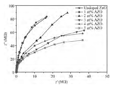
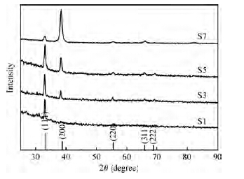
Highly transparent and preferential c-axis oriented nanocrystalline undoped and Al doped zinc oxide (AZO) thin films have been deposited onto amorphous glass substrate by spray pyrolysis. The XRD studies reveal that AZO with a hexagonal (wurtzite) crystal structure having (002) preferred orientation is formed. The atomic force microscope (AFM) shows uniform surface topography. The optical band gap values of undoped and AZO thin films were changed from 3.34 to 3.35 eV. The band gap energy and photoluminescence are found to depend on the Al doping. Thermoelectric power measurement shows film having n-type in nature. Dielectric constant and loss (tan δ) were found to be frequency dependent. Interparticle interactions in the deposited films are studied by complex impendence spectroscopy.


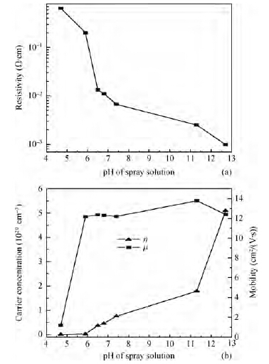
Highly conducting transparent cadmium oxide thin films were prepared by the conventional spray pyrolysis technique. The pH of the spray solution is varied by adding ammonia/hydrochloric acid. The effect of pH on the morphology, crystallinity and optoelectronic properties of these films is studied. The structural analysis showed all the films in the cubic phase. For the films with pH <7 (acidic condition), the preferred orientation is along the (111) direction and for those with pH >7 (alkaline condition), the preferred orientation is along the (200) direction. A lowest resistivity of 9.9 × 10⁻⁴ Ω · cm (with carrier concentration = 5.1 × 1020 cm-3, mobility = 12.4 cm2/(V· s)) is observed for pH ≈ 12. The resistivity is tuned almost by three orders of magnitude by controlling the bath pH with optical transmittance more than 70%. Thus, the electrical conductivity of CdO films could be easily tuned by simply varying the pH of the spray solution without compromising the optical transparency.
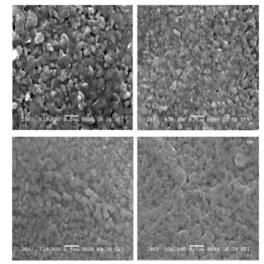
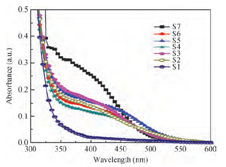
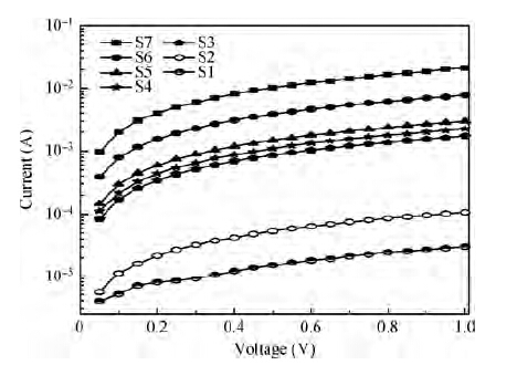

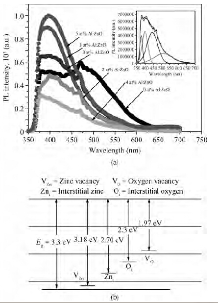
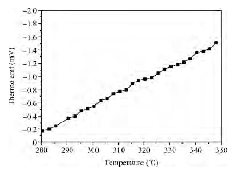
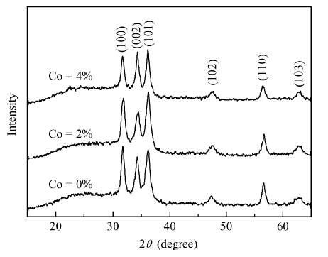
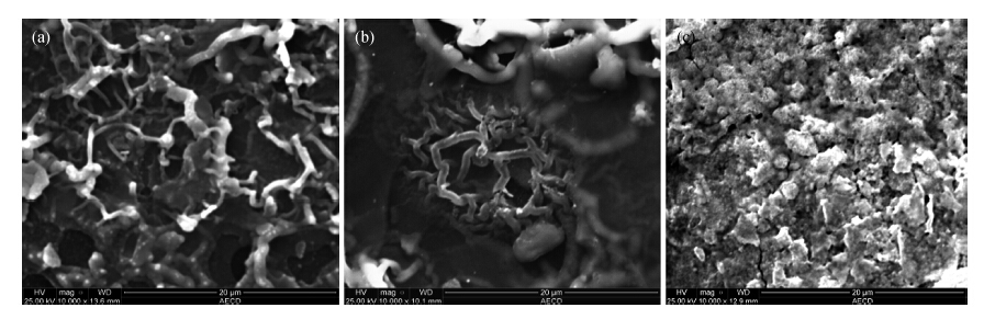
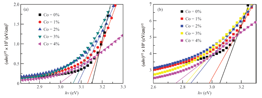
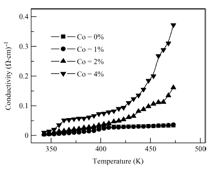
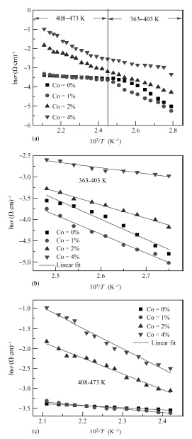
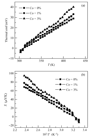
Nanocrystalline Zn1-xCoxO (where x varies from 0 to 0.04 in steps of 0.01) thin films were deposited onto glass substrate by the spray pyrolysis technique at a substrate temperature of 350 ℃. The X-ray diffraction patterns confirm the formation of hexagonal wurtzite structure. The crystal grain size of these films was found to be in the range of 11—36 nm. The scanning electron micrographs show a highly crystalline nanostructure with different morphologies including rope-like morphology for undoped ZnO and nanowalls and semispherical morphology for Co-doped ZnO. The transmittance increases with increasing Co doping. The optical absorption edge is observed in the transmittance spectra from 530 to 692 nm, which is due to the Co2+ absorption bands corresponding to intraionic d—d* shifts. The direct and indirect optical band gap energies decrease from 3.05 to 2.75 eV and 3.18 to 3.00 eV, respectively for 4 mol% Co doping. The electrical conductivity increases with increasing both the Co doping and temperature, indicating the semiconducting nature of these films. The temperature dependence thermal electromotive force measurement indicates that both undoped and Co-doped ZnO thin films show p-type semiconducting behavior near room temperature. This behavior dies out beyond 313 K and they become n-type semiconductors.


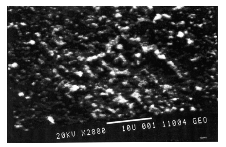
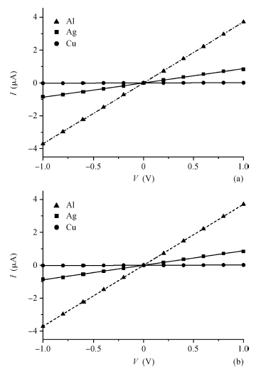
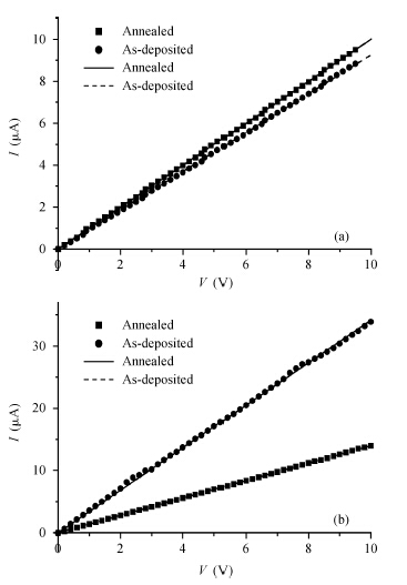
There are several metals that form ohmic contacts for ZnO thin films, such as copper, aluminum and silver. The aim of this work is to make a comparison between these ohmic contacts. To achieve this purpose, polycrystalline ZnO thin films were prepared by the spray pyrolysis technique, and characterized by the I—V measurements at room temperature. Two strips of each metal were thermally evaporated on the surface of the film and measurements were first recorded in the dark and room light, then in the dark before and after annealing for Al, which was found to be the best in the set. Films with aluminum contacts gave the smallest resistivity, best ohmicity and they are slightly affected by light as required. On the other hand, copper was found to be the worst, and films with copper contacts gave the largest resistivity, worst ohmicity and they are the most affected by light. Annealing improved the aluminum contacts due to alloying and doping.


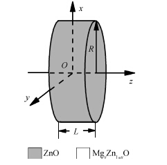
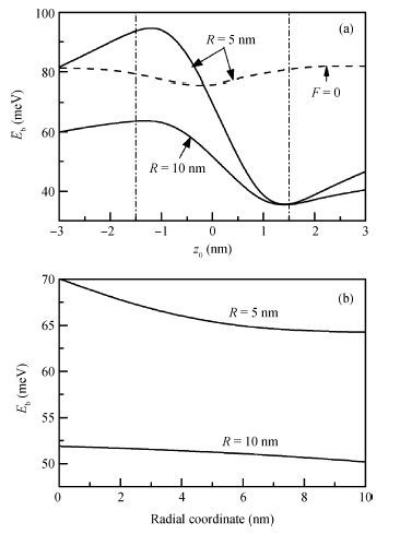
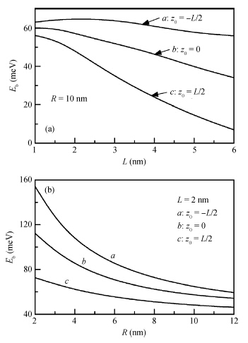
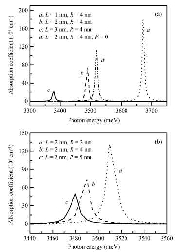
Within the framework of the effective-mass approximation and the dipole approximation, considering the three-dimensional confinement of the electron and hole and the strong built-in electric field (BEF) in strained wurtzite ZnO/Mg0.25Zn0.75O quantum dots (QDs), the optical properties of ionized donor-bound excitons (D+, X) are investigated theoretically using a variational method. The computations are performed in the case of finite band offset. Numerical results indicate that the optical properties of (D+, X) complexes sensitively depend on the donor position, the QD size and the BEF. The binding energy of (D+, X) complexes is larger when the donor is located in the vicinity of the left interface of the QDs, and it decreases with increasing QD size. The oscillator strength reduces with an increase in the dot height and increases with an increase in the dot radius. Furthermore, when the QD size decreases, the absorption peak intensity shows a marked increment, and the absorption coefficient peak has a blueshift. The strong BEF causes a redshift of the absorption coefficient peak and causes the absorption peak intensity to decrease remarkably. The physical reasons for these relationships have been analyzed in depth.


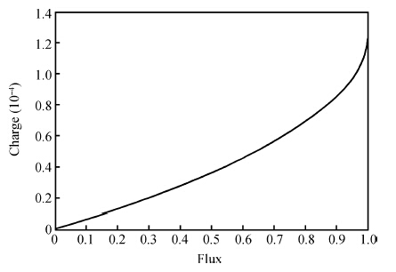
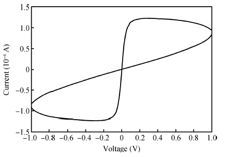
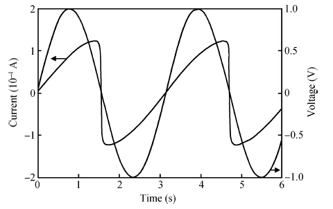
The fourth fundamental circuit element memristor completes the missing link between charge and magnetic flux. It consists of the function of the resistor as well as memory in nonlinear fashion. The property of the memristor depends on the magnitude and direction of applied potential. This unique property makes it the primitive building block for many applications such as resistive memories, soft computing, neuromorphic systems and chaotic circuits etc. In this paper we report TiO2-based nanostructured memristor modelling. The present memristor model is constructed in MATLAB environment with consideration of the linear drift model of memristor. The result obtained from the linear drift model is well matched with earlier reported results by other research groups.


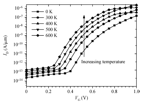
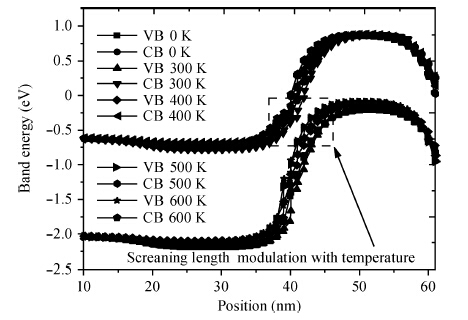
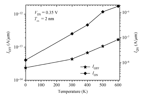
For the first time, we investigate the temperature effect on AlGaAs/Si based hetero-structure junctionless double gate tunnel field effect transistor. Since junctionless tunnel FET is an alternative substitute device for ultra scaled deep-submicron CMOS technology, having very good device characteristics such as an improved subthreshold slope (<60 mV/decade at 300 K) and very small static leakage currents. The improved subthreshold slope and static leakage current confirms that it will be helpful for the development of future low power switching circuits. The 2-D computer based simulation results show that OFF-state leakage current is almost temperature independent for the proposed device structure.


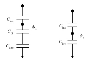
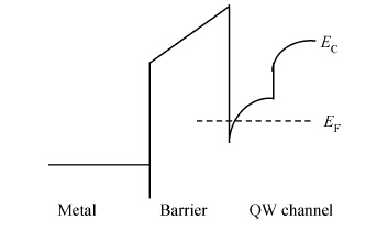
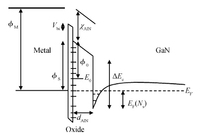
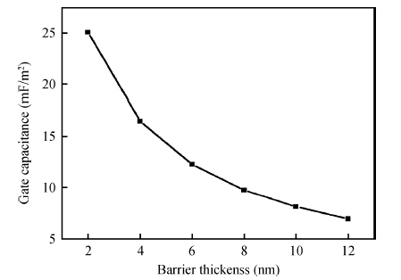
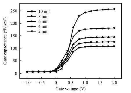
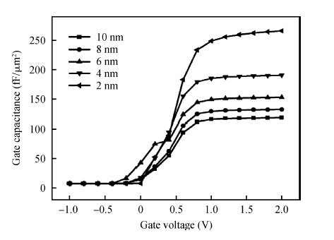
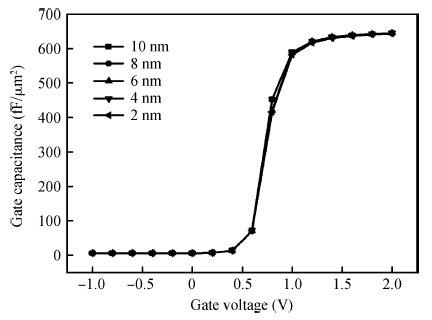
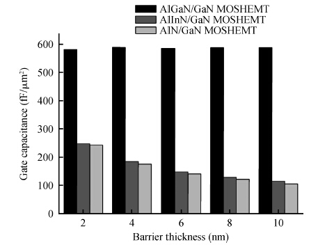
A mathematical model is developed predicting the behavior of gate capacitance with the nanoscale variation of barrier thickness in AlN/GaN MOSHEMT and its effect on gate capacitances of AlInN/GaN and AlGaN/GaN MOSHEMTs through TCAD simulations is compared analytically. AlN/GaN and AlInN/GaN MOSHEMTs have an advantage of a significant decrease in gate capacitance up to 108 fF/μm2 with an increase in barrier thickness up to 10 nm as compared to conventional AlGaN/GaN MOSHEMT. This decrease in gate capacitance leads to improved RF performance and hence reduced propagation delay.

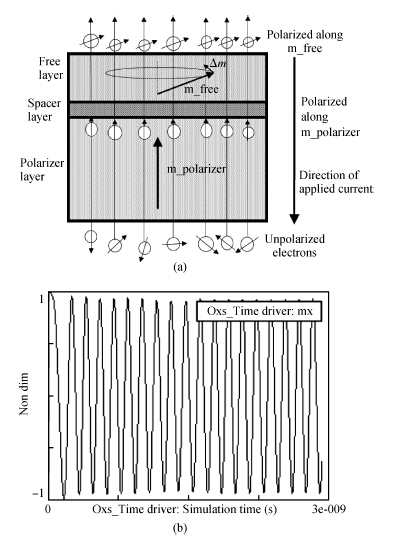
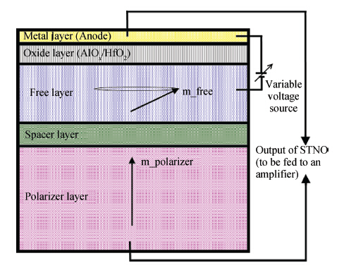
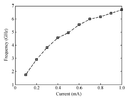
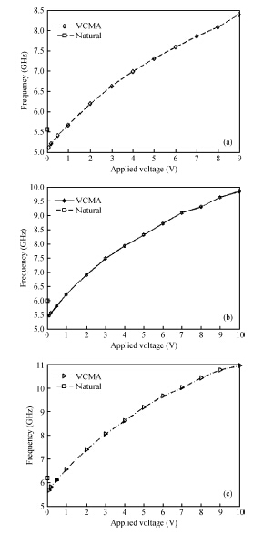
The spin-transfer nano-oscillator (STNO) has recently acquired a huge amount of research interest, due to its promising easy tunability along with the miniature size. The output frequency control of an STNO through magnetic field and current has been examined almost to its full extent; however, there are issues that still need to be addressed. Here, we propose a novel way of voltage control of the output frequency of an STNO, and alongside reducing its power requirement.


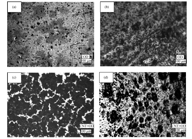
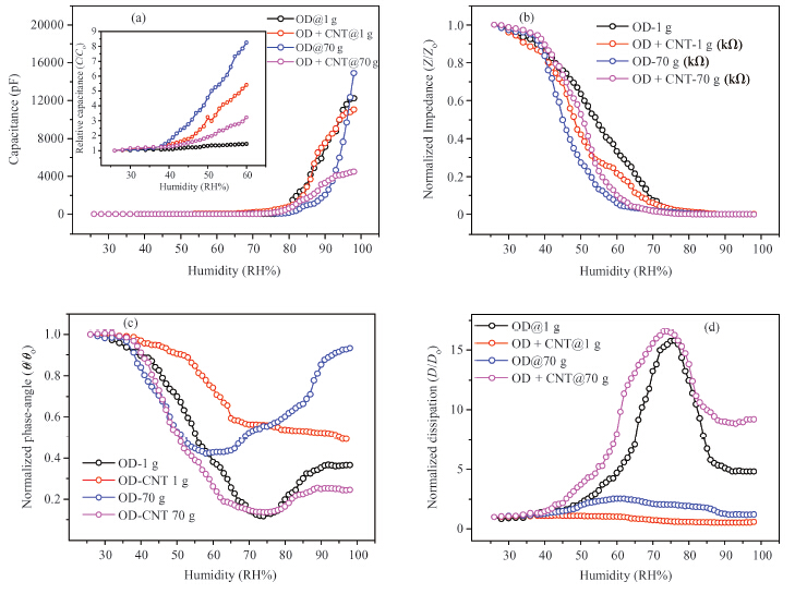
The humidity sensing properties of the thin films of an organic semiconductor material orange dye (OD) and its composite with CNTs deposited at high gravity conditions have been reported. Impedance, phase angle, capacitance and dissipation of the samples were measured at 1 kHz and room temperature conditions. The impedance decreases and capacitance increases with an increase in the humidity level. It was found that the sensitivity of the OD-based thin film samples deposited at high gravity condition is higher than the samples deposited at low gravity condition. The impedances and capacitance sensitivities of the of the samples deposited under high gravity condition are 6.1 times and 1.6 times higher than the films deposited under low gravity condition.

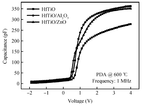
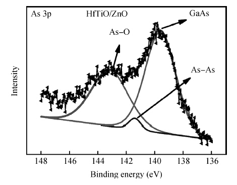
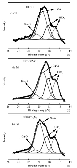
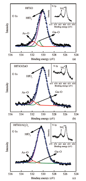
GaAs metal—oxide—semiconductor (MOS) capacitors with HfTiO as the gate dielectric and Al2O3 or ZnO as the interface passivation layer (IPL) are fabricated. X-ray photoelectron spectroscopy reveals that the Al2O3 IPL is more effective in suppressing the formation of native oxides and As diffusion than the ZnO IPL. Consequently, experimental results show that the device with Al2O3 IPL exhibits better interfacial and electrical properties than the device with ZnO IPL: lower interface-state density (7.2 × 10¹² eV-1cm-2), lower leakage current density (3.60 × 10⁻⁷ A/cm2 at Vg = 1 V) and good C—V behavior.


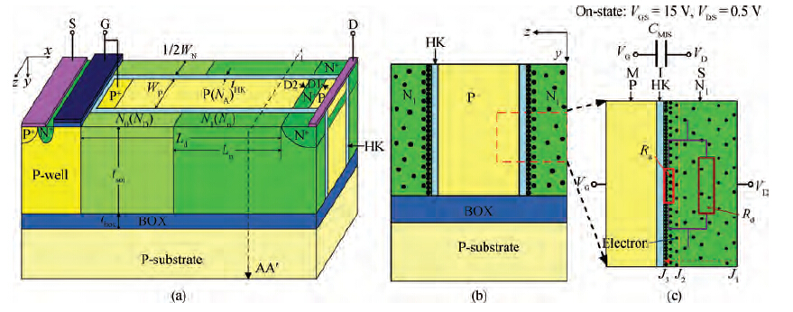
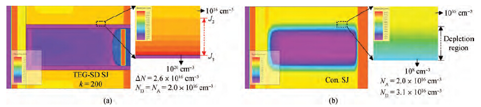
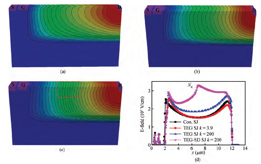
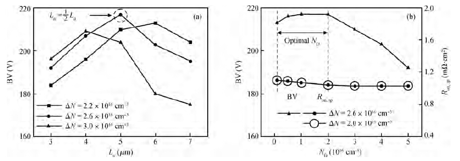
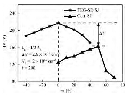
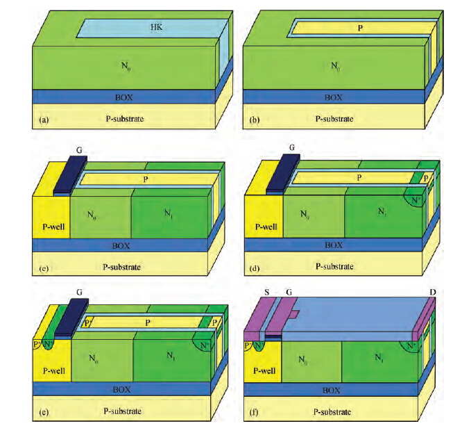
A novel silicon-on-insulator (SOI) super-junction (SJ) LDMOS with an ultra-strong charge accumulation effect is proposed. It has two key features: an assisted-accumulation trench-type extending gate (TEG) with a high-k (HK) dielectric and a step-doped N pillar (TEG-SD SJ LDMOS). In the on-state, electrons accumulate at the sidewall of the HK dielectric from the source to the drain by the TEG. Furthermore, the high permittivity of the HK dielectric leads to an ultra-strong charge accumulation effect. As a result, an ultra-low resistance current path is formed. The specific on-resistance (Ron,sp) is thus greatly reduced and is independent of the drift doping concentration. In the off-state, the step-doped N pillar effectively suppresses the substrate-assisted depletion effect by charge compensation. Moreover, the reshape effect of the HK dielectric and the new electric field (E-field) peak introduced by the step-doped N pillar enhance the drift region E-field. Hence, the BV is improved. Simulation indicates that the TEG-SD SJ LDMOS achieves an extremely low Ron,sp of 1.06 mΩ · cm2 and a BV of 217 V. Compared with the conventional SJ LDMOS, the TEG-SD SJ LDMOS decreases the Ron,sp by 77.5% and increases the BV by 33%, exhibiting a high figure of merits (FOM = BV2/Ron,sp) of 44 MW/cm2.


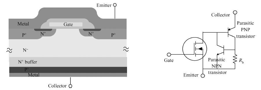
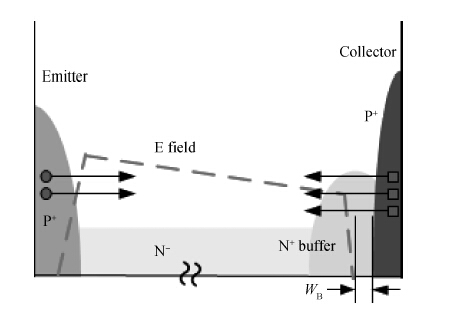
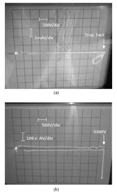
The static avalanche breakdown behavior of 4.5 kV high-voltage IGBT is studied by theory analysis and experiment. The avalanche breakdown behaviors of the 4.5 kV IGBTs with different backside structures are investigated and compared by using the curve tracer. The results show that the snap back behavior of the breakdown waveform is related to the bipolar PNP gain, which leads to the deterioration of the breakdown voltage. There are two ways to optimize the backside structure, one is increasing the implant dose of the N+ buffer layer, the other is decreasing the implant dose of the P+ collector layer. It is found that the optimized structure is effective in suppressing the snap back behavior and improving the breakdown characteristic of high voltage IGBT.

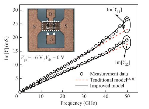
Given the coplanar waveguide (CPW) effect on AlGaN/GaN high electron mobility transistors at a high frequency, the traditional equivalent circuit model cannot accurately describe the electrical characteristics of the device. The admittance of CPW capacitances is large when the frequency is higher than 40 GHz; its impact on the device cannot be ignored. In this study, a small-signal equivalent circuit model considering CPW capacitance is provided. To verify the model, S-parameters are obtained from the modeling and measurements. A good agreement is observed between the simulation and measurement results, indicating the reliability of the model.


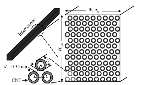
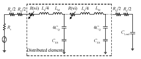
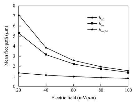
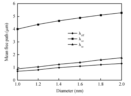
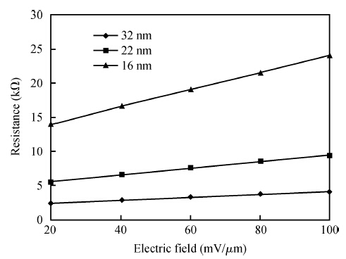
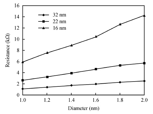
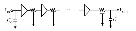
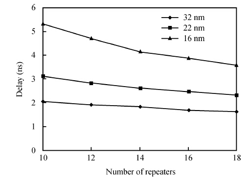
The influence of an electric field on metallic single walled carbon nanotube (SWCNT) interconnects is studied. A voltage-dependent equivalent circuit model is presented for the impedance parameters of single-wall carbon nanotubes that capture various electron—phonon scattering mechanisms as a function of the electric field. To estimate the performance of SWCNT bundle interconnects, signal delay and power dissipation are calculated based on the field dependent model that results in an improvement in the delay and power estimation accuracy compared to the field-independent model. We find that the power delay product of a SWCNT bundle increases with the increase in electric field but decreases with technology scaling showing that at a low electric field, the SWCNT bundle is a potential reliable alternative interconnect for future high performance VLSI industry at scaled technologies.


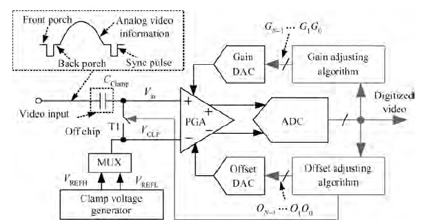
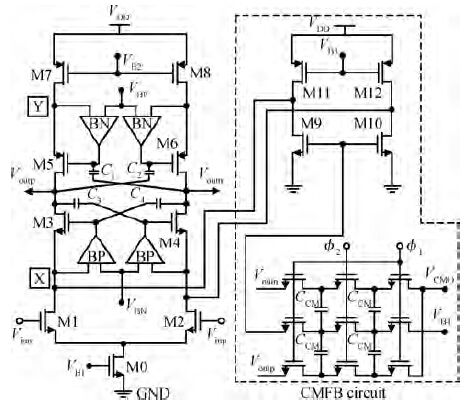
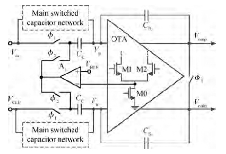
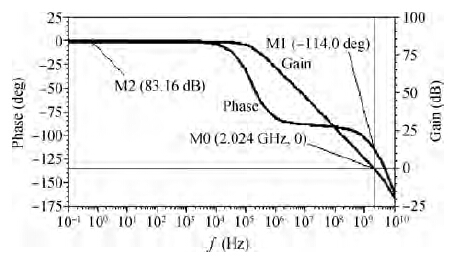
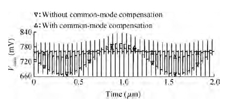
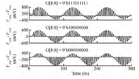
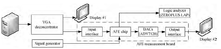
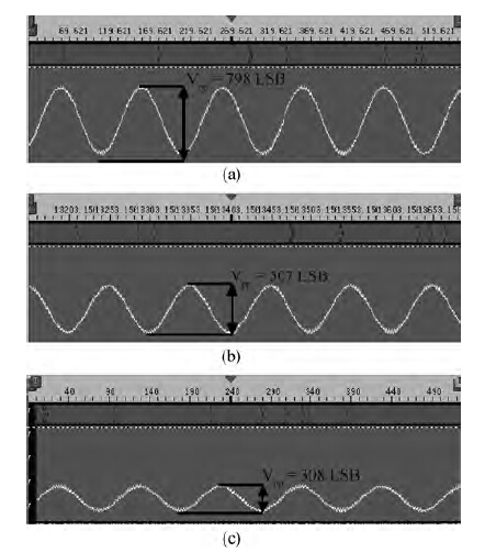
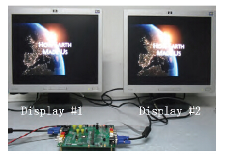
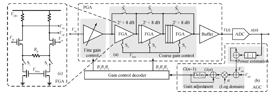
A multifunctional programmable gain amplifier (PGA) that provides gain and offset adjusting abilities for high-definition video analog front-ends (AFE) is presented. With a switched-capacitor structure, the PGA also acts as a sample and holder of the analog-to-digital converter (ADC) in the AFE to reduce the power consumption and chip area of the whole AFE. Furthermore, the PGA converts the single-ended video signal into differential signal for the following ADC to reject common-mode noise and interferences. The 9-bit digital-to-analog converter (DAC) for gain and offset adjusting is embedded into the switched capacitor networks of the PGA. A video AFE integrated circuit based on the proposed PGA is fabricated in a 0.18-μm process. Simulation and measurement results show that the PGA achieves a gain control range of 0.90 to 2.34 and an offset control range of —220 to 220 mV while consuming 10.1 mA from a 1.8 V power supply.


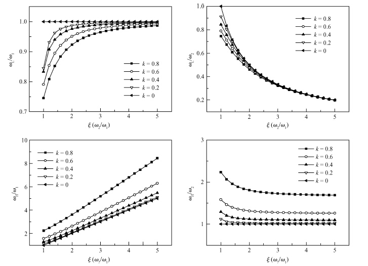
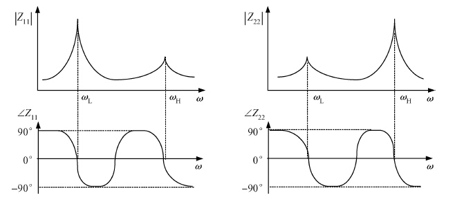
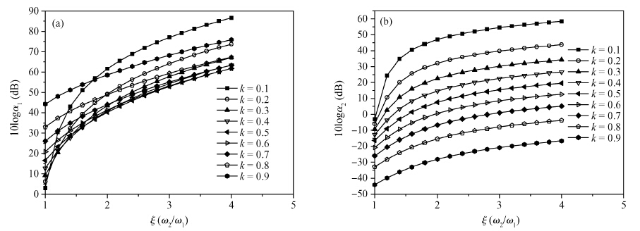
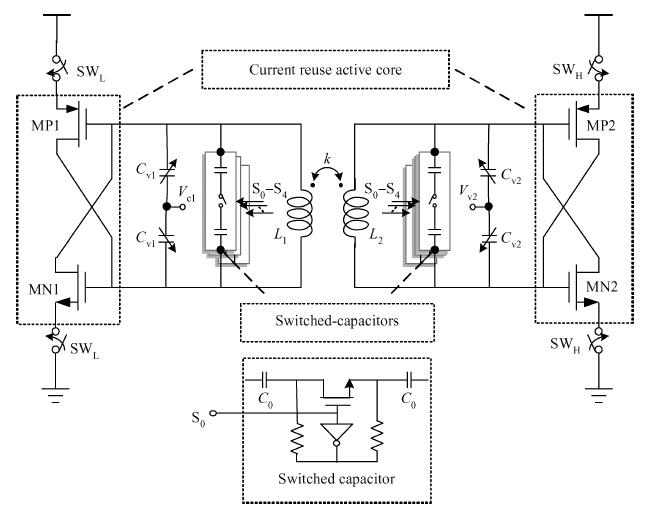
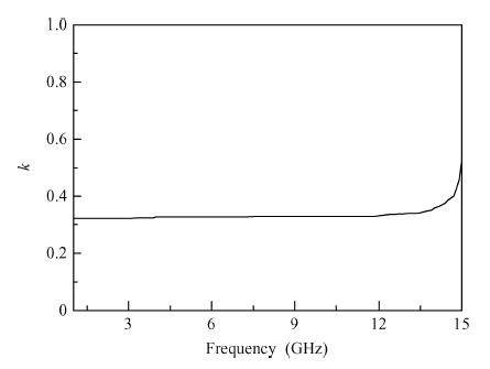
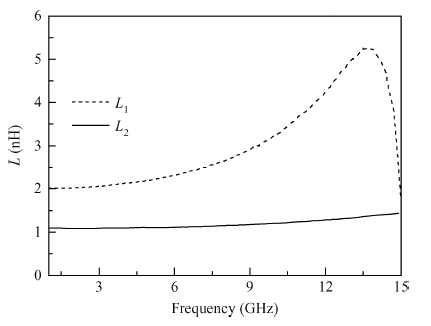
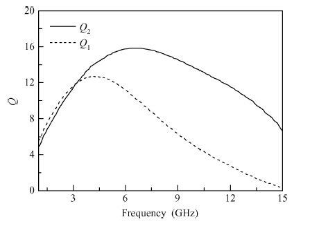
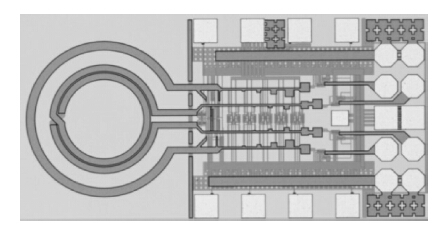
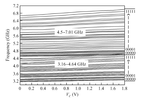
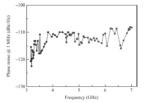
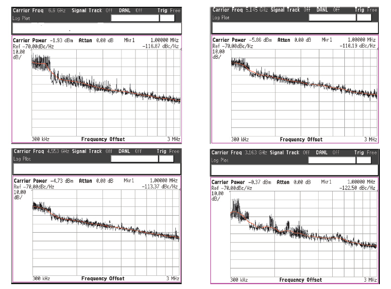
A dual-band, wide tuning range voltage-controlled oscillator that uses transformer-based fourth-order (LC) resonator with a compact common-centric layout is presented. Compared with the traditional wide band (VCO), it can double frequency tuning range without degrading phase noise performance. The relationship between the coupling coefficient of the transformer, selection of frequency bands, and the quality factor at each band is investigated. The transformer used in the resonator is a circular asymmetric concentric topology. Compared with conventional octagon spirals, the proposed circular asymmetric concentric transformer results in a higher quality-factor, and hence a lower oscillator phase noise. The VCO is designed and fabricated in a 0.18-μm CMOS technology and has 75% wide tuning range of 3.16—7.01 GHz. Depending on the oscillation frequency, the VCO current consumption is adjusted from 4.9 to 6.3 mA. The measured phase noises at 1 MHz offset from carrier frequencies of 3.1, 4.5, 5.1, and 6.6 GHz are —122.5, —113.3, —110.1, and —116.8 dBc/Hz, respectively. The chip area, including the pads, is 1.2 × 0.62 mm2 and the supply voltage is 1.8 V.


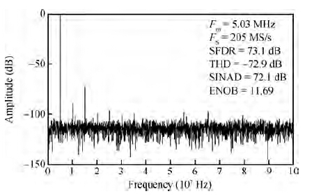
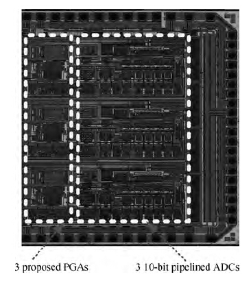
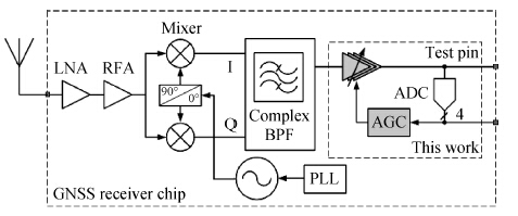
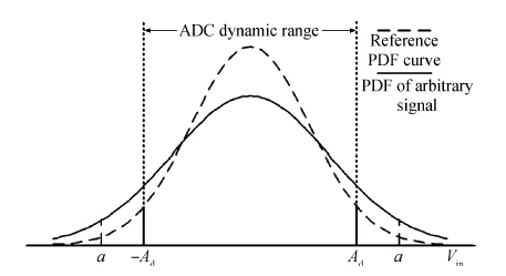
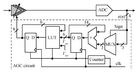
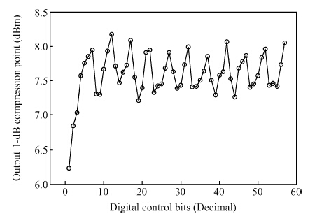
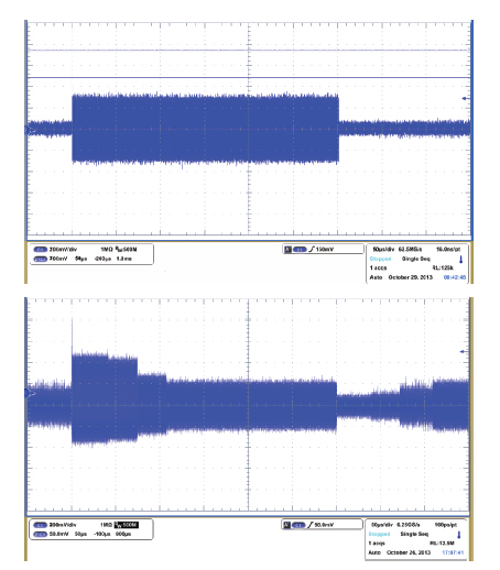
A novel digitally controlled automatic gain control (AGC) loop circuitry for the global navigation satellite system (GNSS) receiver chip is presented. The entire AGC loop contains a programmable gain amplifier (PGA), an AGC circuit and an analog-to-digital converter (ADC), which is implemented in a 0.18 μm complementary metal—oxide—semiconductor (CMOS) process and measured. A binary-weighted approach is proposed in the PGA to achieve wide dB-linear gain control with small gain error. With binary-weighted cascaded amplifiers for coarse gain control, and parallel binary-weighted trans-conductance amplifier array for fine gain control, the PGA can provide a 64 dB dynamic range from -4 to 60 dB in 1.14 dB gain steps with a less than 0.15 dB gain error. Based on the Gaussian noise statistic characteristic of the GNSS signal, a digital AGC circuit is also proposed with low area and fast settling. The feed-backward AGC loop occupies an area of 0.27 mm2 and settles within less than 165 μs while consuming an average current of 1.92 mA at 1.8 V.


This paper describes a new silicon physical unclonable function (PUF) architecture that can be fabricated on a standard CMOS process. Our proposed architecture is built using process sensors, difference amplifier, comparator, voting mechanism and diffusion algorithm circuit. Multiple identical process sensors are fabricated on the same chip. Due to manufacturing process variations, each sensor produces slightly different physical characteristic values that can be compared in order to create a digital identification for the chip. The diffusion algorithm circuit ensures further that the PUF based on the proposed architecture is able to effectively identify a population of ICs. We also improve the stability of PUF design with respect to temporary environmental variations like temperature and supply voltage with the introduction of difference amplifier and voting mechanism. The PUF built on the proposed architecture is fabricated in 0.18 μm CMOS technology. Experimental results show that the PUF has a good output statistical characteristic of uniform distribution and a high stability of 98.1% with respect to temperature variation from —40 to 100 ℃, and supply voltage variation from 1.7 to 1.9 V.

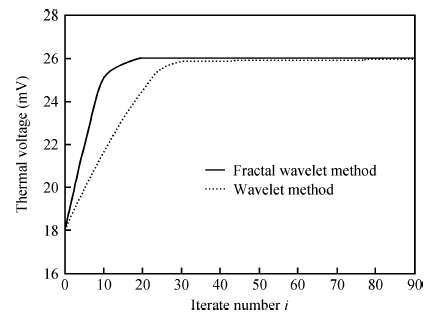

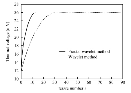
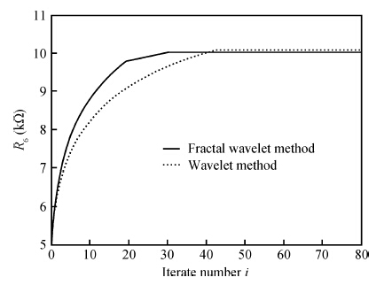
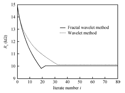
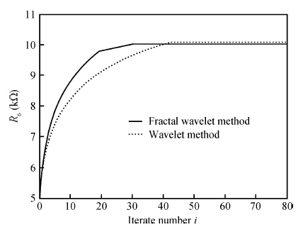


Aiming at the problem of parameter estimation in analog circuits, a new approach is proposed. The approach is based on the fractional wavelet to derive the Volterra series model of the circuit under test (CUT). By the gradient search algorithm used in the Volterra model, the unknown parameters in the CUT are estimated and the Volterra model is identified. The simulations show that the parameter estimation results of the proposed method in the paper are better than those of other parameter estimation methods.

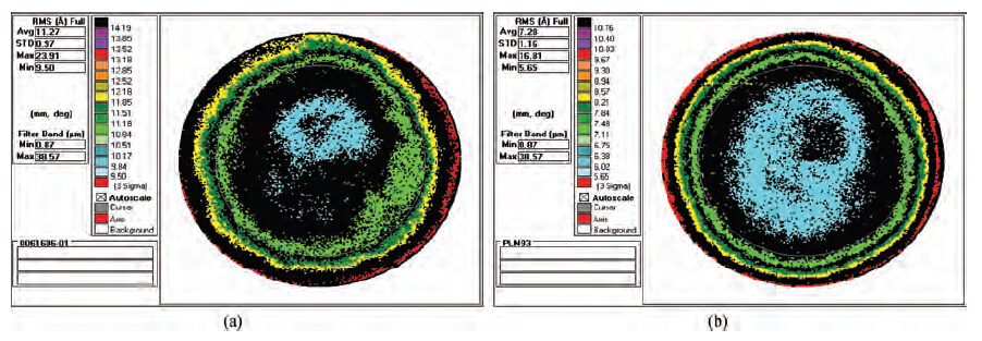
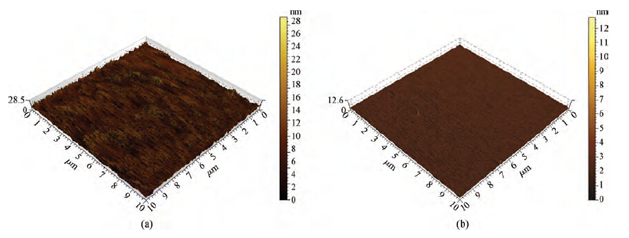
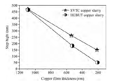
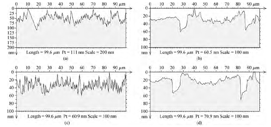
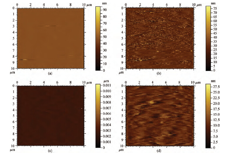
We observed and analyzed the acid and HEBUT alkaline of Cu chemical mechanical polishing (CMP) slurry to evaluate their effects. Material analysis has shown that the planarity surfaces and the removal rate of alkaline slurry are better than the acid slurry during metal CMP processes. The global surface roughness and the small-scale surface roughness by 10 × 10 μm2 of copper film polished by the SVTC slurry are 1.127 nm and 2.49 nm. However, it is found that the surface roughnesses of copper films polished by the HEBUT slurry are 0.728 nm and 0.215 nm. All other things being equal, the remaining step heights of copper films polished by the SVTC slurry and HEBUT slurry are respectively 150 nm and 50 nm. At the end of the polishing process, the dishing heights of the HEBUT slurry and the SVTC slurry are approximately both 30 nm, the erosion heights of the HEBUT slurry and the SVTC slurry are approximately both 20 nm. The surface states of the copper film after CMP are tested, and the AFM results of two samples are obviously seen. The surface polished by SVTC slurry shows many spikes. This indicates that the HEBUT alkaline slurry is promising for inter-level dielectric (ILD) applications in ultra large-scale integrated circuits (ULSI) technology.


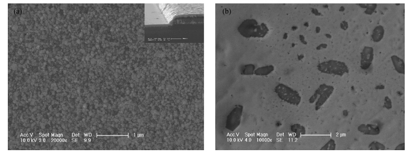
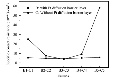
The multi-layer metals of Ni/AuGe/Pt/Au with a Pt diffusion barrier layer of ohmic contact to n-GaAs were studied. The surface morphology and ohmic contact resistivity of multi-layer metals were characterized, with and without the Pt diffusion barrier layer for comparison. The SEM and EDS measurements show the Pt diffusion barrier layer can block the interdiffusion of atoms in multi-layer metals, and improve the surface morphology. The TLM results show that the samples with a Pt diffusion barrier layer have uniform ohmic contact resistance, indicating that the Pt diffusion barrier layer can increase the repetition and uniformity of ohmic contact to n-GaAs, and improve the thermal stability and reliability of GaAs-based devices.


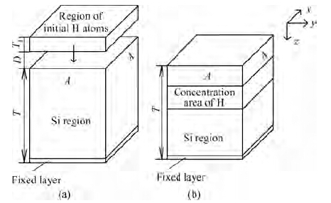
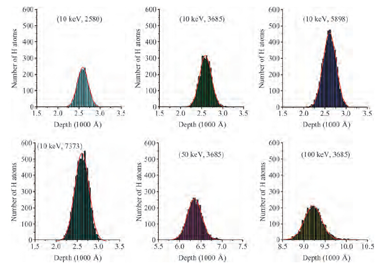
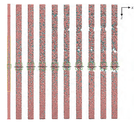
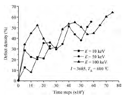
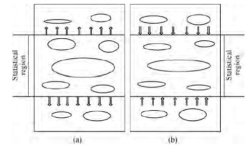
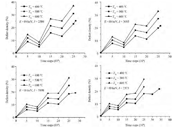
Defect evolution in a single crystal silicon which is implanted with hydrogen atoms and then annealed is investigated in the present paper by means of molecular dynamics simulation. By introducing defect density based on statistical average, this work aims to quantitatively examine defect nucleation and growth at nanoscale during annealing in Smart-Cut® technology. Research focus is put on the effects of the implantation energy, hydrogen implantation dose and annealing temperature on defect density in the statistical region. It is found that most defects nucleate and grow at the annealing stage, and that defect density increases with the increase of the annealing temperature and the decrease of the hydrogen implantation dose. In addition, the enhancement and the impediment effects of stress field on defect density in the annealing process are discussed.


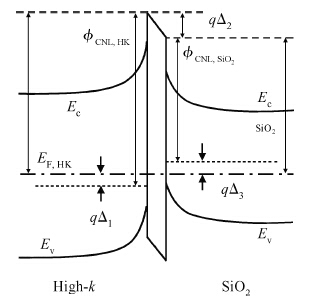
The formation of an electric dipole at the high-k/SiO2 interface is quantitatively analyzed. The band lineups and physical origin of dipole formation at the high-k/SiO2 interface are explained by the dielectric contact induced gap states (DCIGS). The charge neutrality level (CNL) of the DCIGS, which represents a distribution of high-k and SiO2 contact induced gap states, is utilized to study the dipole moment. The charge transfer due to different CNLs of high-k and SiO2 is considered as the dominant origin of dipole formation. The theoretically calculated dipole strengths of high-k/SiO2 systems based on this model are in good agreement with the experimental data.