This paper reviews the geometric resistivity correction factor of the 4-point probe DC electrical conductivity measurement method using several geometrical samples. During the review of the literature, only the articles that include the effect of geometry on resistivity calculation were considered. Combinations of equations used for various geometries were also given. Mathematical equations were given in the text without details. Expressions for the most commonly used geometries were presented in a table for easy reference.
Issue Browser
Volume 36, Issue 8,
Aug 2015


J. Semicond.
2015, 36(8): 082002 doi: 10.1088/1674-4926/36/8/082002

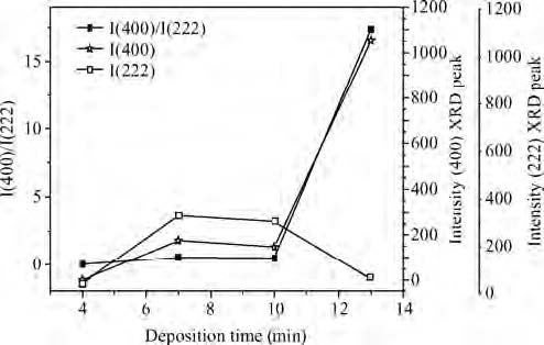
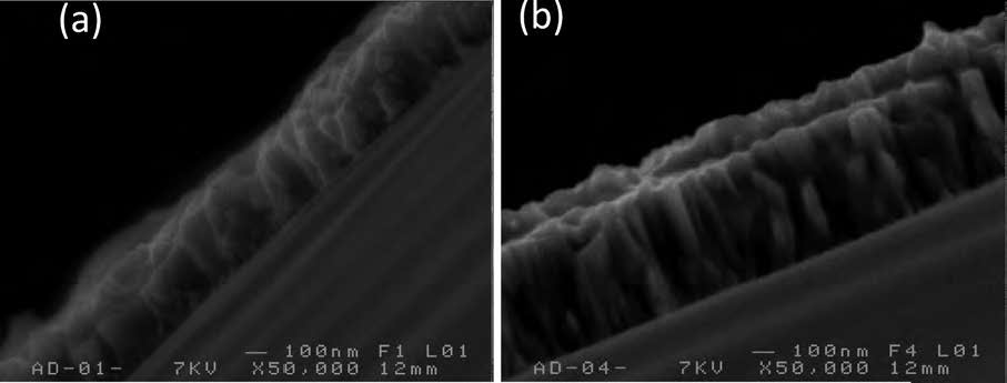
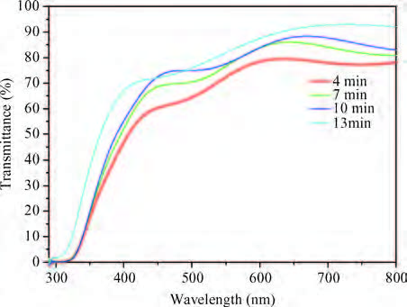
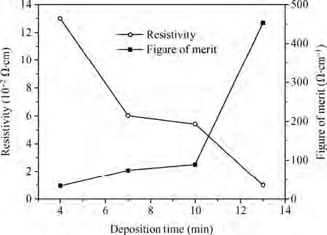
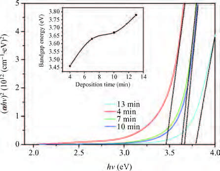
Indium oxide (In2O3) thin films are successfully deposited on glass substrate at different deposition times by an ultrasonic spray technique using Indium chloride as the precursor solution; the physical properties of these films are characterized by XRD, SEM, and UV-visible. XRD analysis showed that the films are polycrystalline in nature having a cubic crystal structure and symmetry space group Ia3 with a preferred grain orientation along the (222) plane when the deposition time changes from 4 to 10 min, but when the deposition time equals 13 min we found that the majority of grains preferred the (400) plane. The surface morphology of the In2O3 thin films revealed that the shape of grains changes with the change of the preferential growth orientation. The transmittance improvement of In2O3 films was closely related to the good crystalline quality of the films. The optical gap energy is found to increase from 3.46 to 3.79 eV with the increasing of deposition time from 4 to 13 min. The film thickness was varied between 395 and 725 nm. The film grown at 13 min is found to exhibit low resistivity (10-2 Ω·cm), and relatively high transmittance (~ 93%).


J. Semicond.
2015, 36(8): 082003 doi: 10.1088/1674-4926/36/8/082005

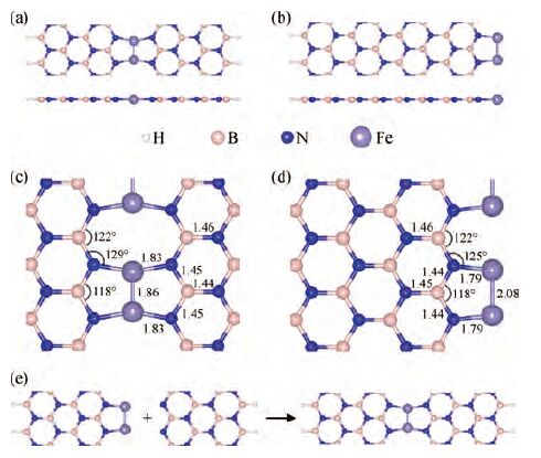
First-principles calculations have been used to research the electronic structure and magnetic properties of zigzag boron nitride nanoribbons (ZBNNRs) terminated/jointed by armchair dimer-Fe chains (respectively called Fe-terminated ZBNNRs and Fe-jointed ZBNNRs). The Fe-terminated ZBNNRs is a semiconductor for different ribbon widths, and the Fe-jointed ZBNNRs become half-metallic regardless of the ribbon width. The magnetism of both structures mainly stems from the Fe atoms. It is found that the self-metallicity of the Fe-jointed ZBNNRs results from the strong interaction between the 3d orbitals of Fe atoms and the 2p orbitals of N atoms. The stability of the Fe-jointed ZBNNRs under room temperature has been confirmed by molecular dynamics simulation. This kind of half-metal property means a selectivity for the two different electrons, it can be applied to spintronics devices. Other transition-metal jointed ZBNNRs are also studied, which can be metals, half-metals or semiconductors with different ground states.


J. Semicond.
2015, 36(8): 082004 doi: 10.1088/1674-4926/36/8/082004

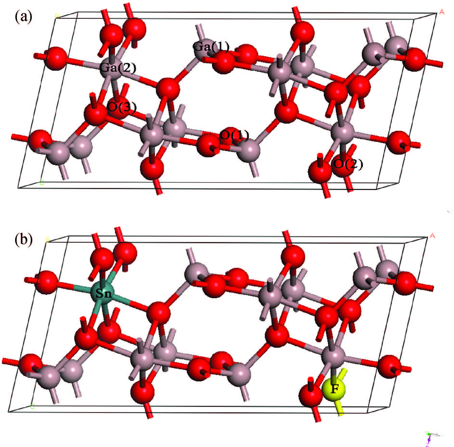
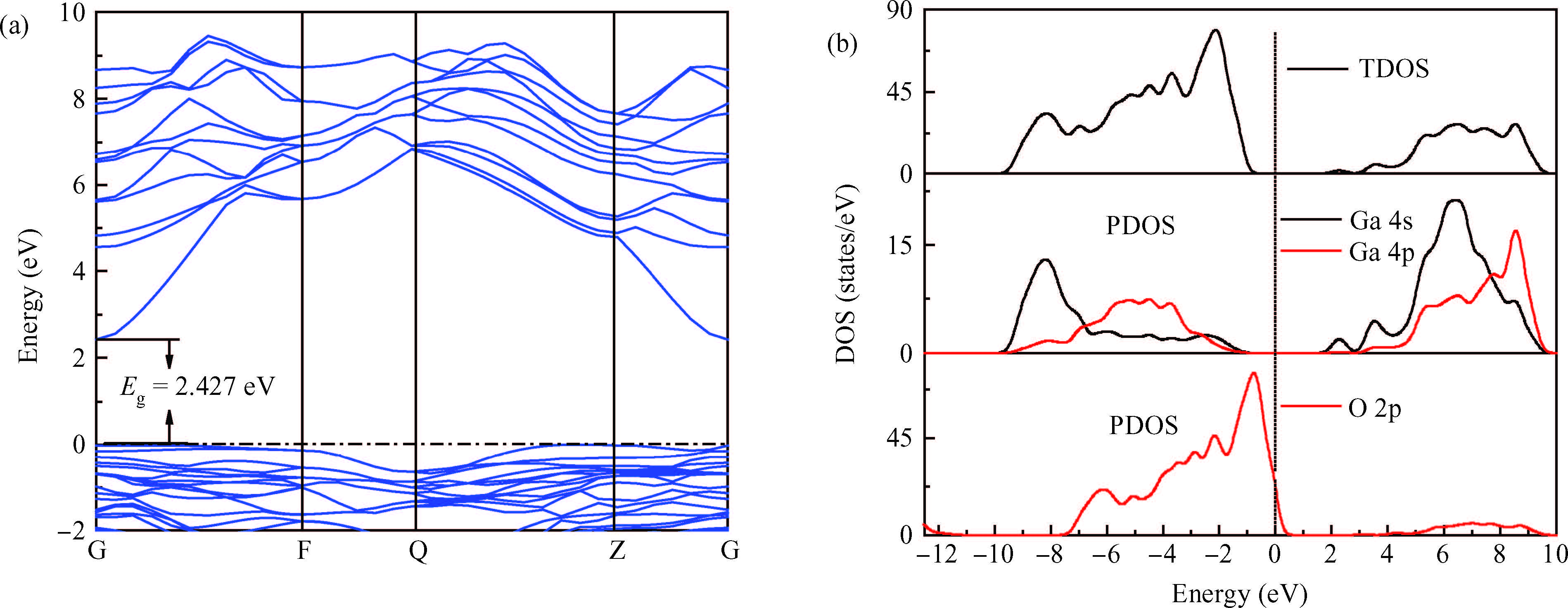
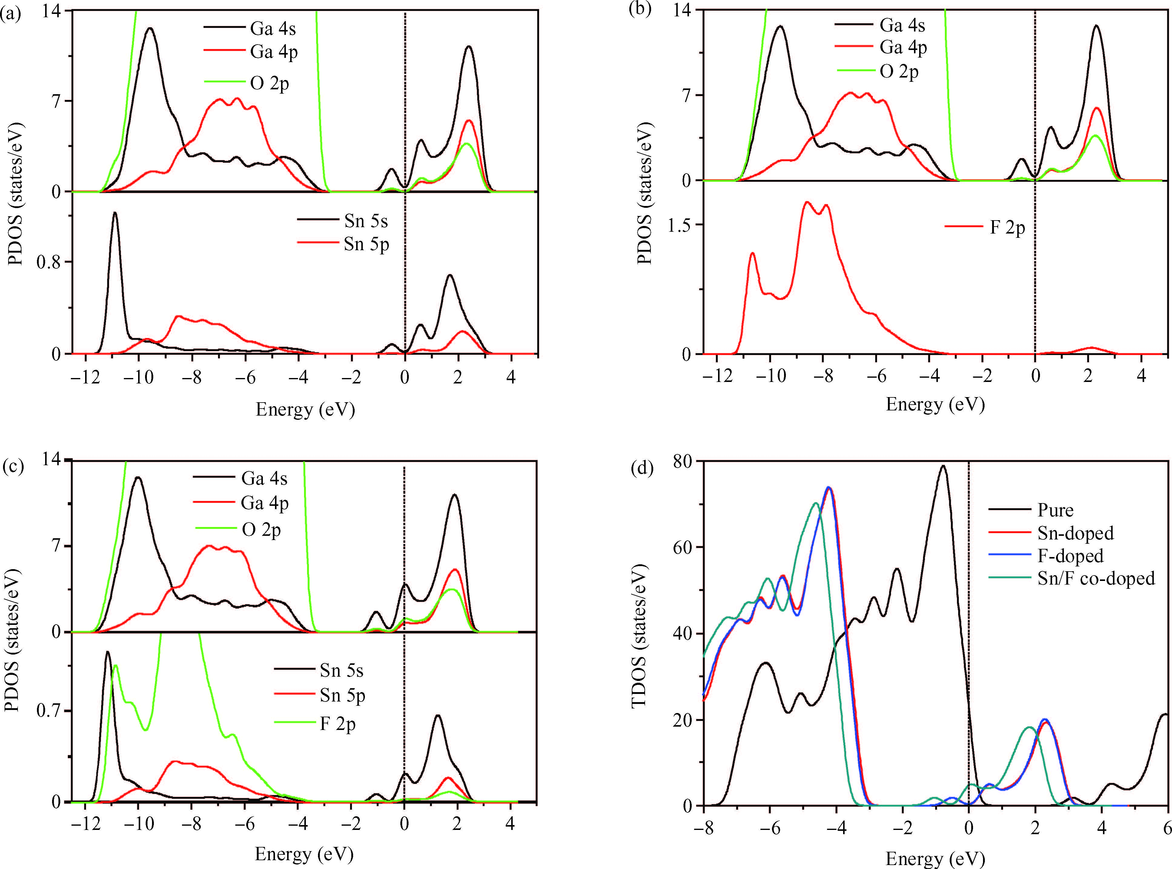
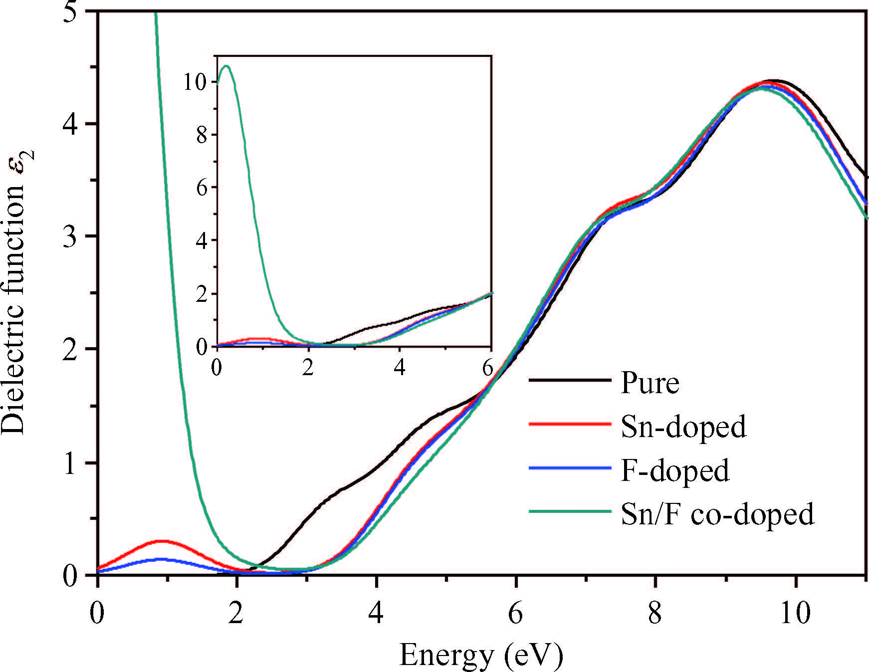
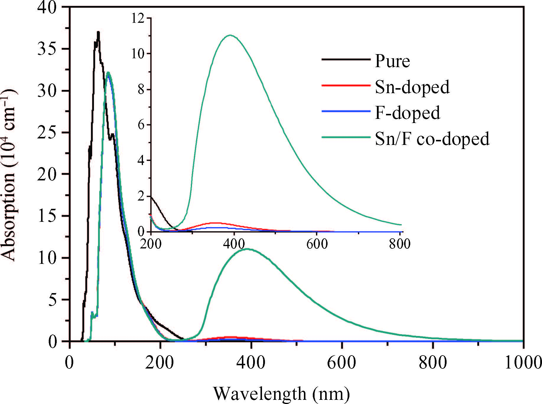
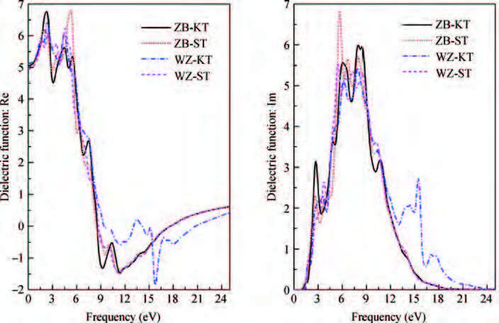
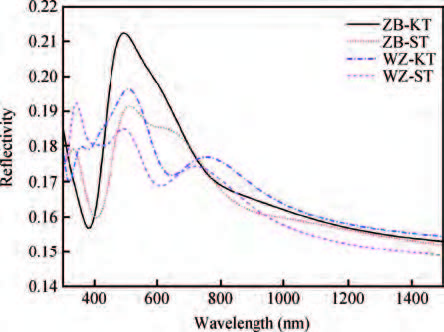
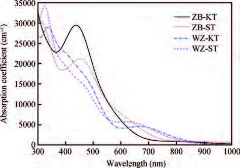
Defect formation energies, electronic structures and optical properties of Sn-doped β-Ga2O3, F-doped β-Ga2O3, and Sn/F co-doped β-Ga2O3 were calculated using the first-principles. The calculated results of the pure and Sn-doped β-Ga2O3 using the local-density approximation (LDA) method show that the lattice parameters and electronic structures are in agreement with previous data. The defect formation energies demonstrate that the doped systems are relatively easy to form under O-rich conditions. Sn-doping, F-doping and Sn/F co-doping make β-Ga2O3 become an n-type semiconductor. Sn/F co-doping β-Ga2O3 has the smallest effective electron mass and the biggest relative electron number, which is expected to possess good conductivity. Sn/F co-doping β-Ga2O3 displays an intense absorption in visible light.
J. Semicond.
2015, 36(8): 083001 doi: 10.1088/1674-4926/36/8/083001

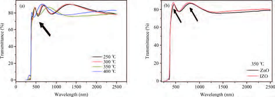
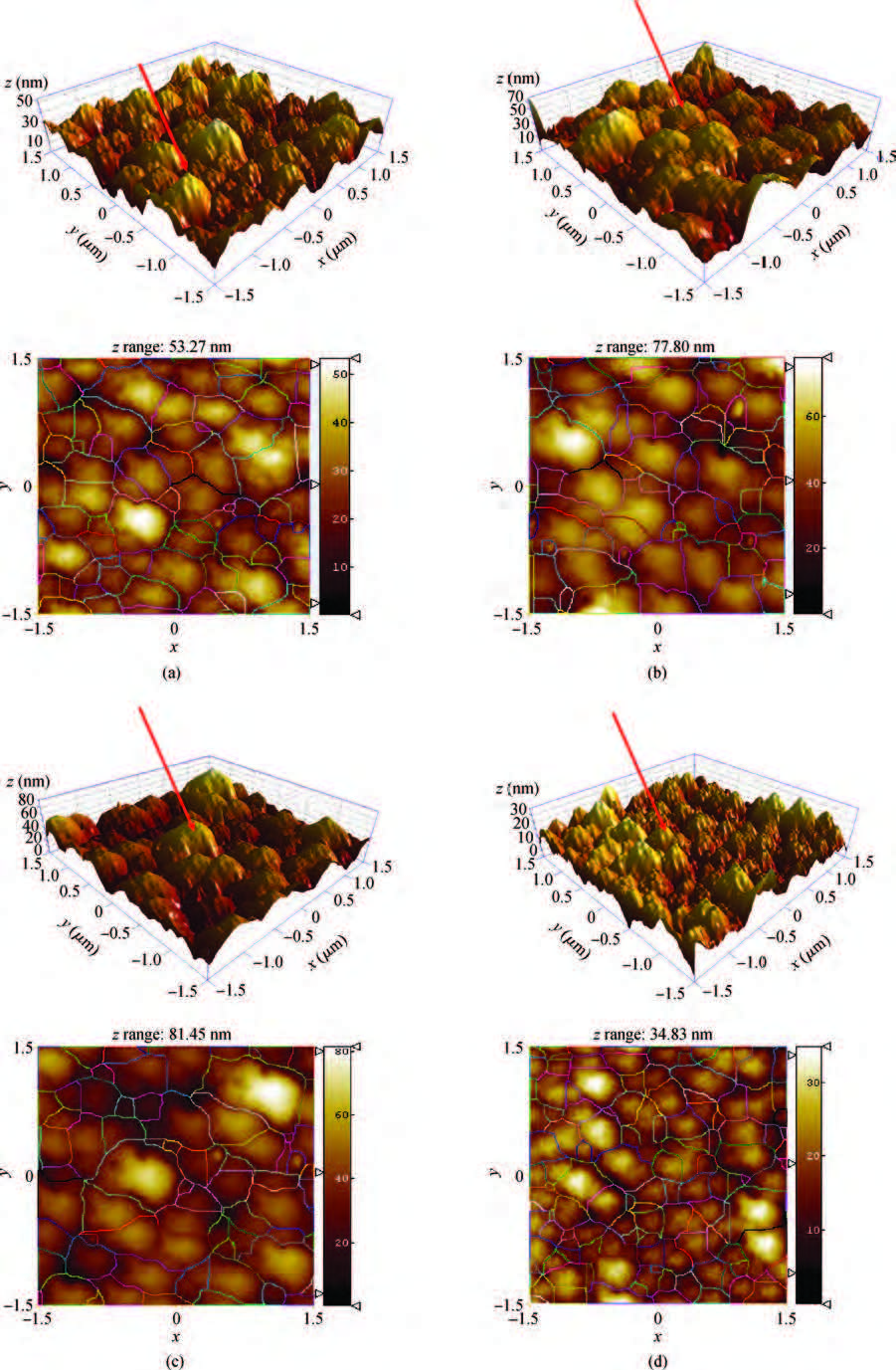
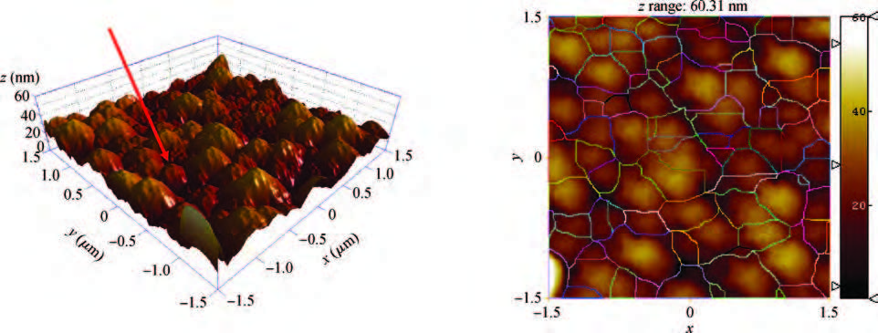
We synthesized the pure and indium-doped (IZO) ZnO films with a facile composition control spray pyrolysis route. The substrate temperature (Ts) and In-doping effects on the properties of as-grown films are investigated. The X-ray pattern confirms that the as-synthesized ZnO phase is grown along a (002) preferential plane. It is revealed that the crystalline structure is improved with a substrate temperature of 350 ℃. Moreover, the morphology of as-grown films, analyzed by AFM, shows nanostructures that have grown along the c-axis. The (3 × 3μm2) area scanned AFM surface studies give the smooth film surface RMS <40 nm. The UV-VIS-IR measurements reveal that the sprayed films are highly transparent in the visible and IR bands. The photoluminescence analysis shows that the strong blue and yellow luminescences of 2.11 and 2.81 eV are emitted from ZnO and IZO films with a slight shift in photon energy caused by In-doping. The band gap is a bit widened by In-doping, 3.21 eV (ZnO) and 3.31 eV (IZO) and the resistivity is reduced from 385 to 8 Ω ·m. An interesting result is the resistivity linear dependence on the substrate temperature of pure ZnO films.


J. Semicond.
2015, 36(8): 083002 doi: 10.1088/1674-4926/36/8/083002

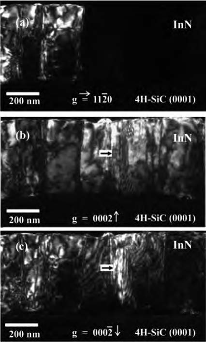
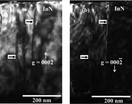
InN film was grown on 4H-SiC (0001) substrate by RF plasma-assisted molecular beam epitaxy (RF-MBE). Prior to the growth of InN film, an InN buffer layer with a thickness of ~ 5.5 nm was grown on the substrate. Surface morphology, microstructure and structural quality of InN film were investigated. Micro-structural defects, such as stacking faults and anti-phase domain in InN film were carefully investigated using transmission electron microscopy (TEM). The results show that a high density of line contrasts, parallel to the growth direction (c-axis), was clearly observed in the grown InN film. Dark field TEM images recorded with diffraction vectors g = 11$\overline{2}$0 and g = 0002 revealed that such line contrasts evolved from a coalescence of the adjacent misoriented islands during the initial stage of the InN nucleation on the substrate surface. This InN nucleation also led to a generation of anti-phase domains.


J. Semicond.
2015, 36(8): 083003 doi: 10.1088/1674-4926/36/8/083003

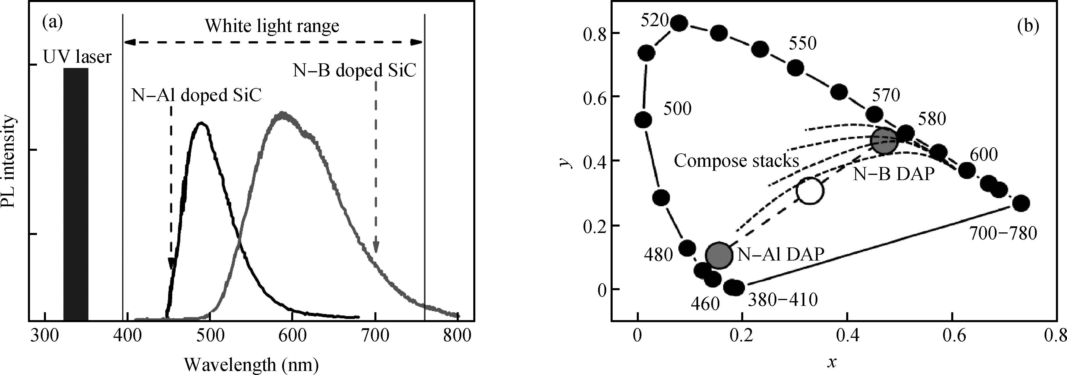
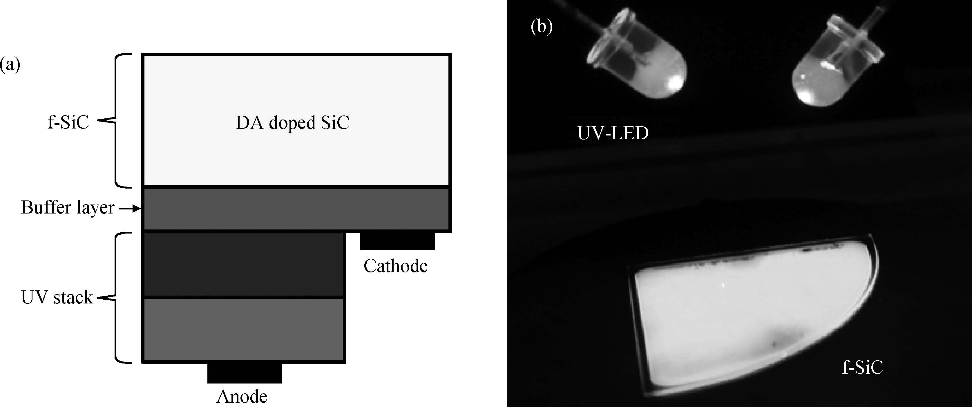
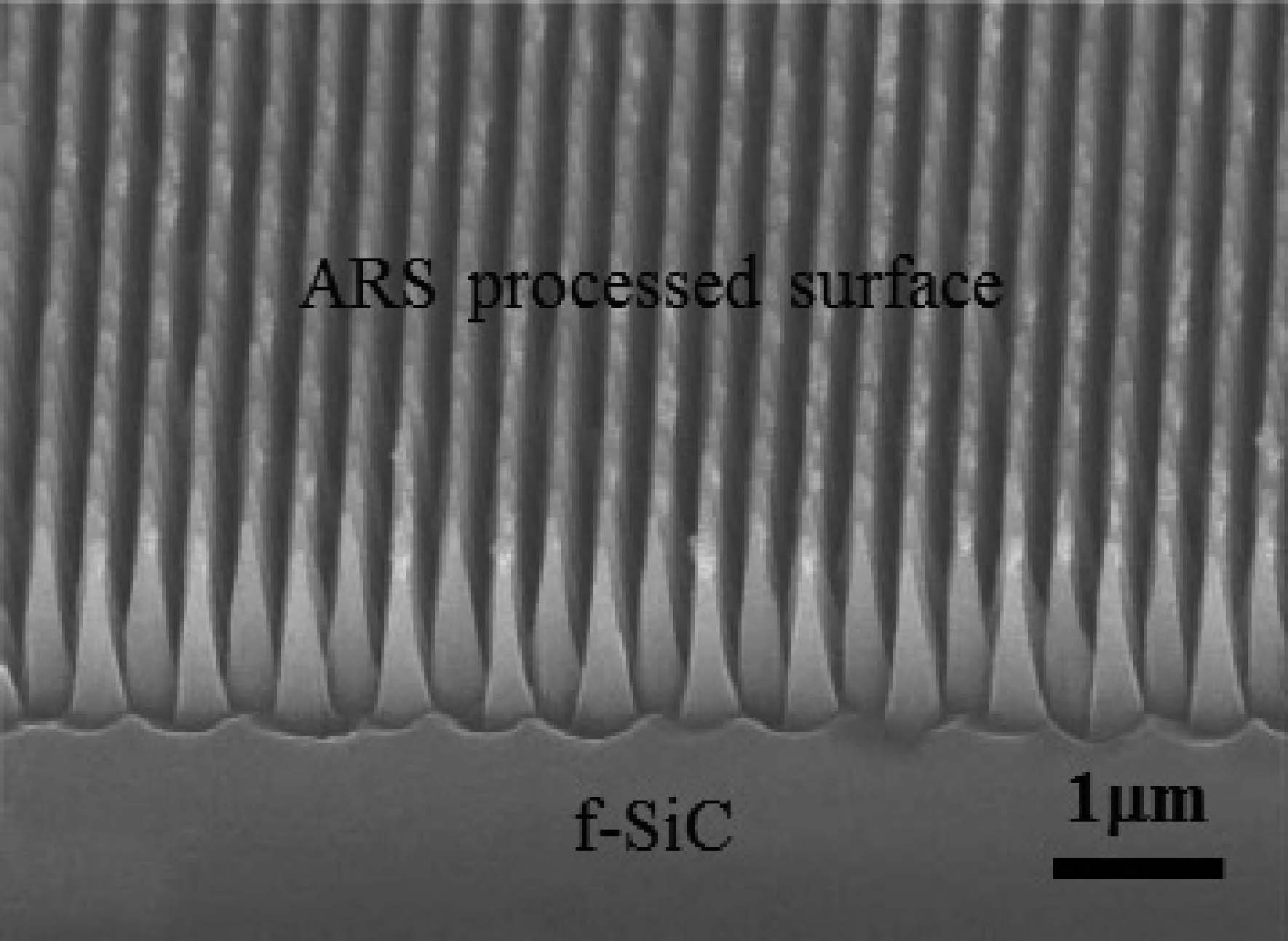
This paper reviewed the advances in fluorescent SiC codoped with nitrogen, boron and aluminum dopants applied to optoelectronics in recent years. The progress aspects in research of the fluorescent property, recombination theory, experiment, and construction design were discussed. The advantages that fluorescent SiC based white LEDs compared with conventional white LEDs were analyzed. It was confirmed that fluorescent SiC is a promising material to replace phosphor in the luminous field. Finally, the problems in the study of fluorescent 4H-SiC were pointed out.


J. Semicond.
2015, 36(8): 083004 doi: 10.1088/1674-4926/36/8/083004

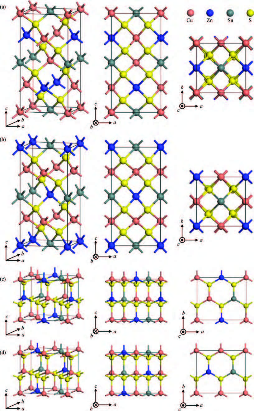
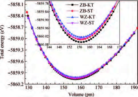
The structural, electronic, optical, and mechanical properties of Cu2ZnSnS4 with four crystal structures are calculated using the density functional theory. No significant difference is observed between the calculated optical and mechanical properties of the considered four crystal structures. The calculated results are in agreement with available reported experimental data. According to the calculated results, the fundamental band gap of Cu2ZnSnS4 is mainly determined by the bandwidth of the isolated conduction band. The effective-mass of carriers of Cu2ZnSnS4 are very small, especially the effective-mass of electrons on the bottom of the conduction band of zincblende-derived Cu2ZnSnS4. Using the calculated elastic constants matrix, the Born stability criteria is shown to be satisfied, and the high B/G ratio indicates that Cu2ZnSnS4 is prone to ductile behavior.


J. Semicond.
2015, 36(8): 083005 doi: 10.1088/1674-4926/36/8/083005

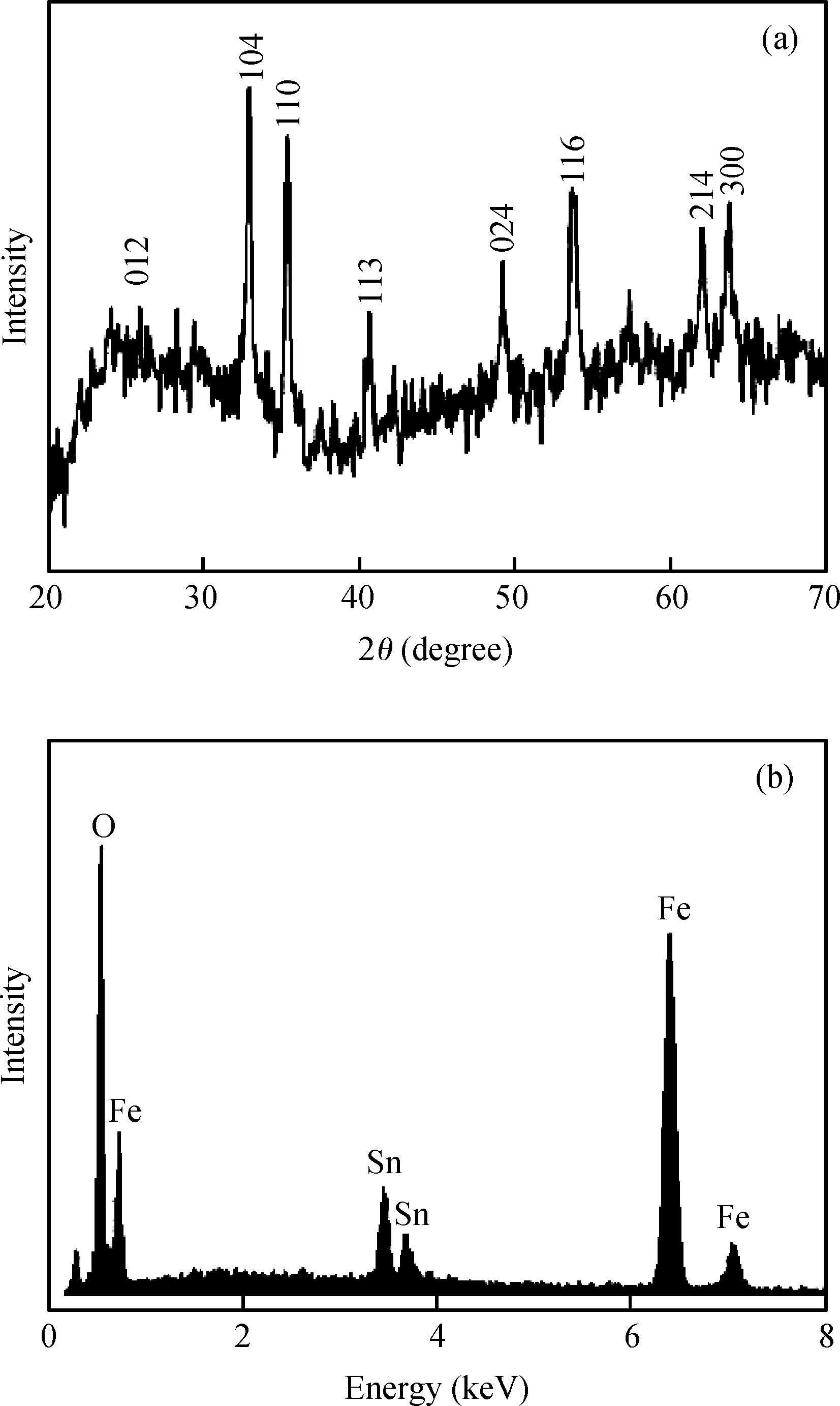
SnO2-doped α-Fe2O3 patulous microtubes (SFPNs) are synthesized by an electrospinning method. The as-synthesized materials are characterized by scanning electron microscope, X-ray powder diffraction and energy dispersive spectroscopy. The gas sensing results show SFPNs possess an excellent sensing property to formaldehyde. The response value of SFPNs gas sensor to 50 ppm formaldehyde is 25.4 at 220 ℃. The lowest detecting limit of 1 ppm formaldehyde is 3.2. Response and recovery characteristic curves of SFPNs gas sensors to 1, 2, 3, 5, 5, 3, 2 and 1 ppm formaldehyde are also tested. The results show a good reversibility and repeatability of SFPNs gas sensors. The sensor exhibits a high selectivity in the presence of acetone, ethanol, toluene, ammonia, hydrogen, carbon monoxide and butane. Moreover, the sensor has a good long-time stability.


J. Semicond.
2015, 36(8): 083006 doi: 10.1088/1674-4926/36/8/083006

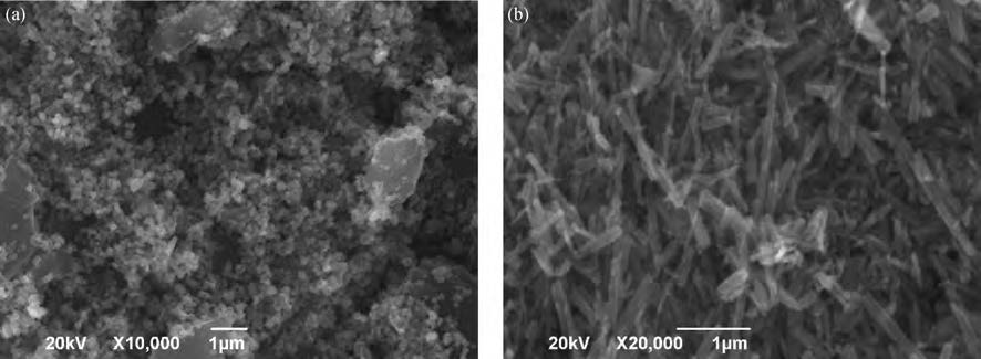
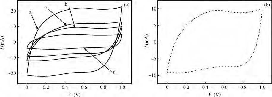
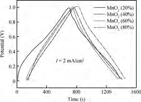
Ruthenium oxide and manganese oxide nanomaterials were respectively prepared by a sol-gel process and hydrothermal synthesis method. The morphologies and microstructures of the composite nanomaterials were characterized by SEM and XRD. Based on the cyclic voltammetry, electrochemical impedance spectroscopy and constant current charge-discharge techniques, the performances of the electrodes were investigated. The results show that the composite of manganese oxide and ruthenium oxide is beneficial to improve the impedance characteristic. The electrode with 60% (mass ratio) manganese oxide has a high specific capacitance of 438 F/g and a lower inner resistance of 0.304 Ω using 38% (mass ration) H2SO4 solution. The capacitance retention of RuO2/MnO2 composite electrode was 92.5% after 300 cycles.


J. Semicond.
2015, 36(8): 083007 doi: 10.1088/1674-4926/36/8/083007

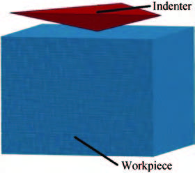
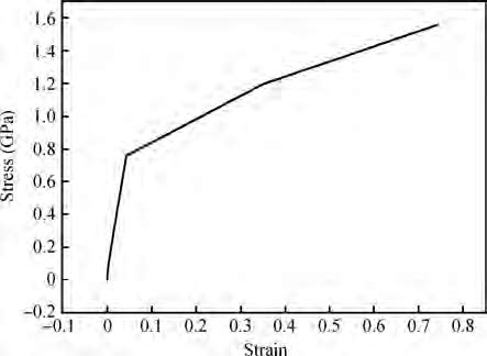
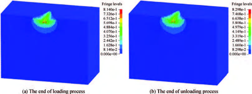
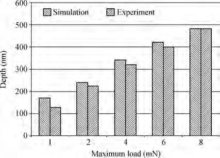
In order to avoid the defects of mesh distortion when dealing with large deformation problems through using the finite element method, a mess-free simulation method——smooth particle hydrodynamics (SPH) has been introduced. The material constitutive model of KDP crystal has been established based on the elastic-plastic theory. Then the nano-indentation on the (001) face of KDP crystal has been carried out using SPH method. Simulation results show that the maximum equivalent stress and the maximum plastic strain concentrate on the area that located near the tip of the indenter during the loading process. The distribution shape of Von Mises stress is similar to concentric circles. During the unloading process, no obvious variation of plastic strain distribution exists. The maximum Von Mises stress is mainly located at the indentation and its edge at the end of the unloading process. The approximate direct proportion relationship between the maximum indentation depth and the depth of the maximum Von Mises stress distribution has been discovered when the maximum load is lower than 8 mN. In addition, the nano-indentation experiments on KDP crystal's (001) face have been carried out. Both the material parameters and the adjusted stress-strain curve have been verified. The hindering role of the affected layer has been found and analyzed.


J. Semicond.
2015, 36(8): 084001 doi: 10.1088/1674-4926/36/8/084001

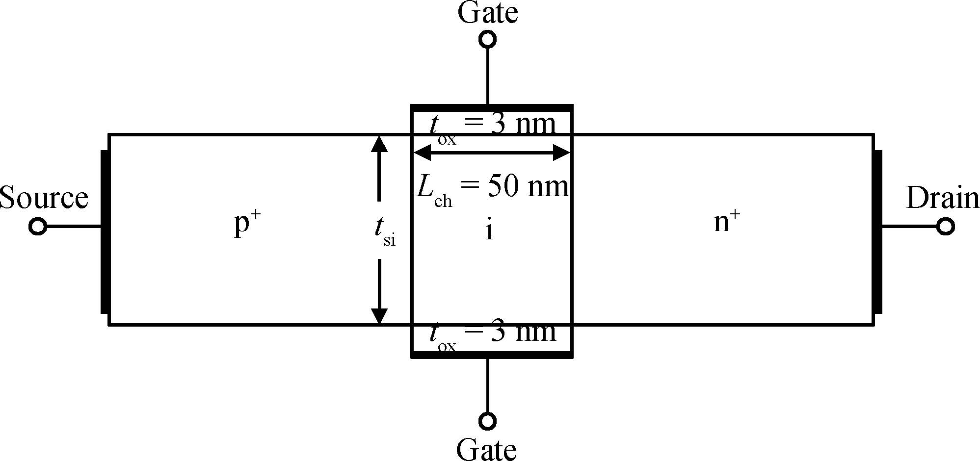
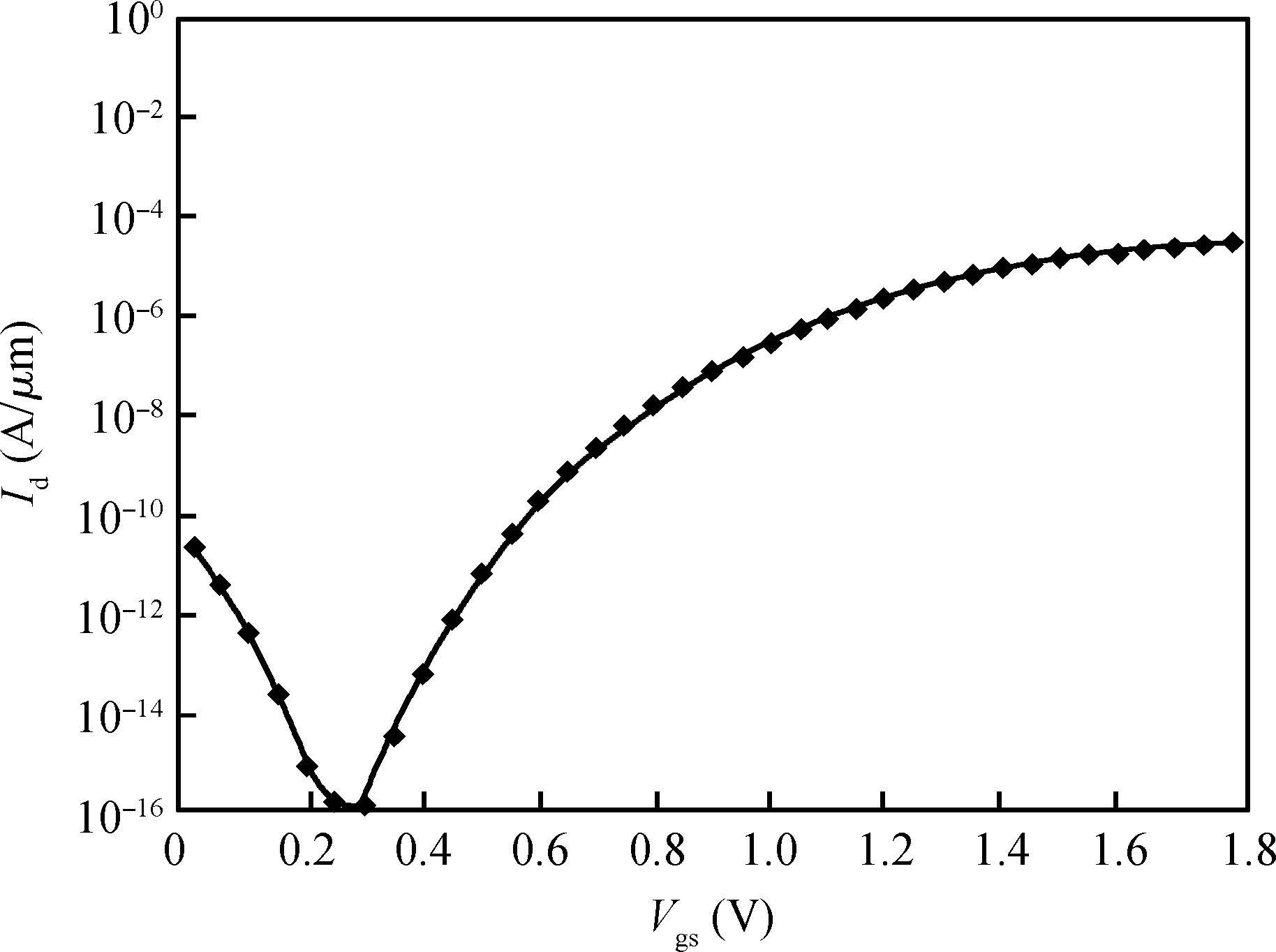
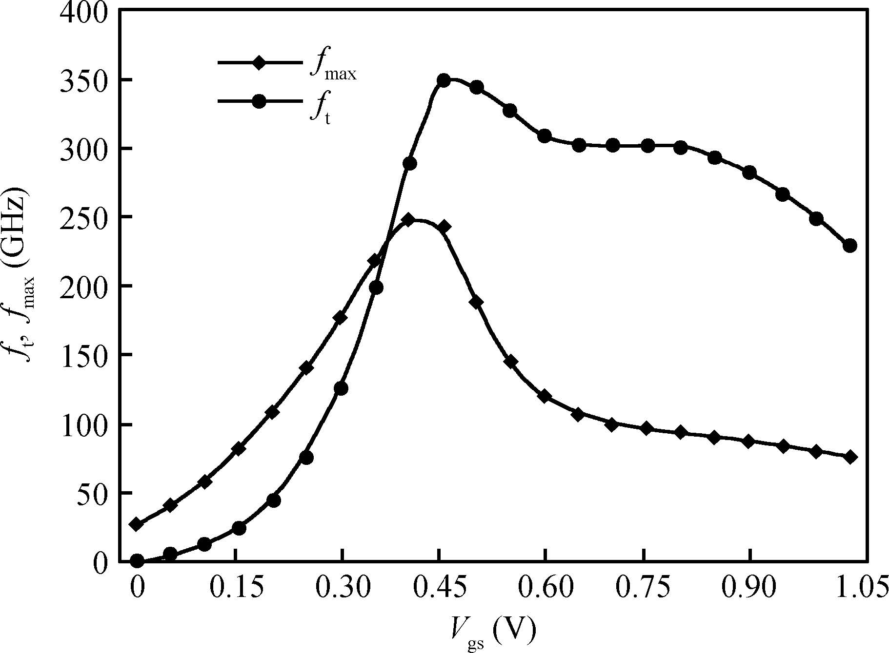
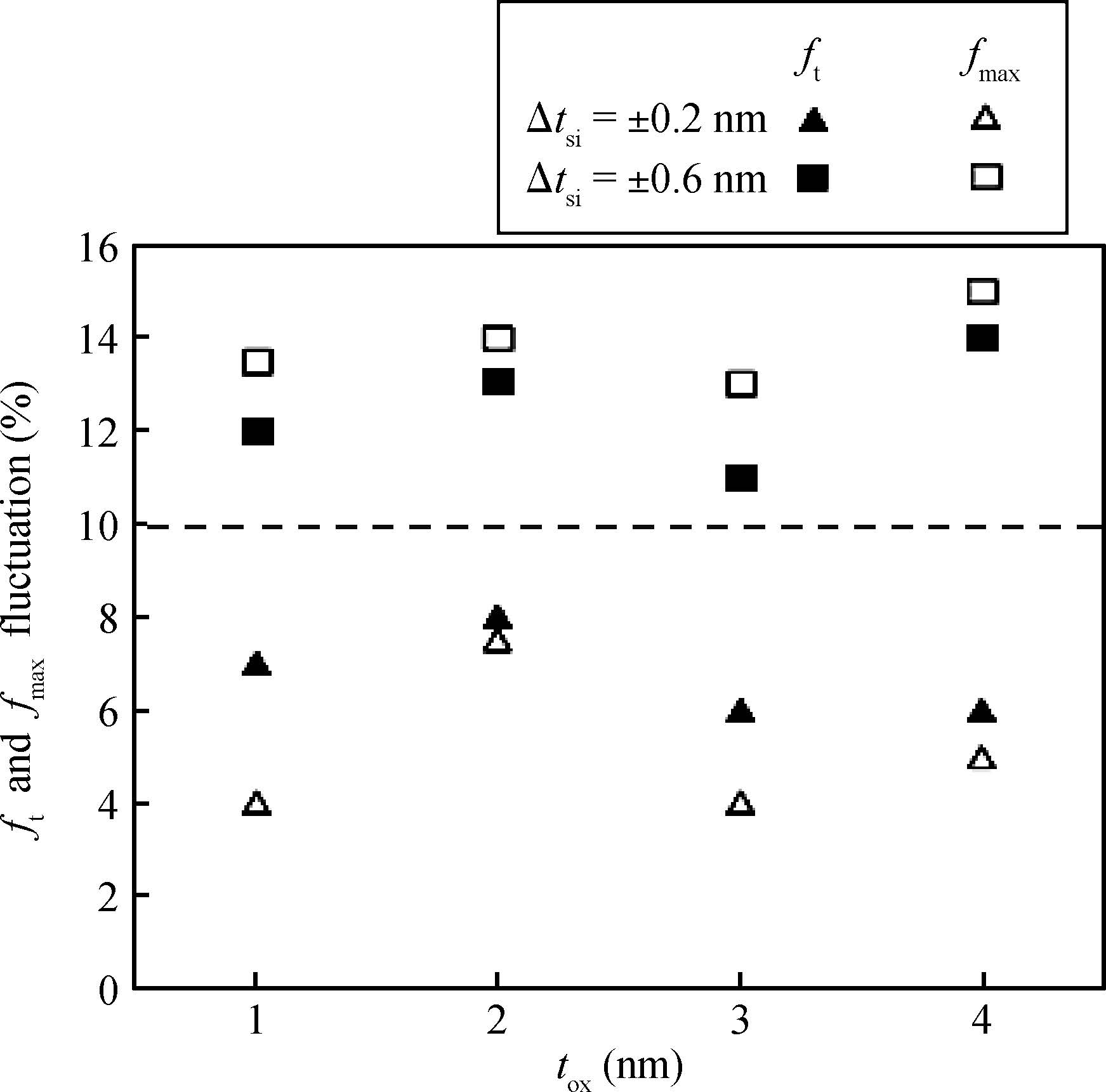
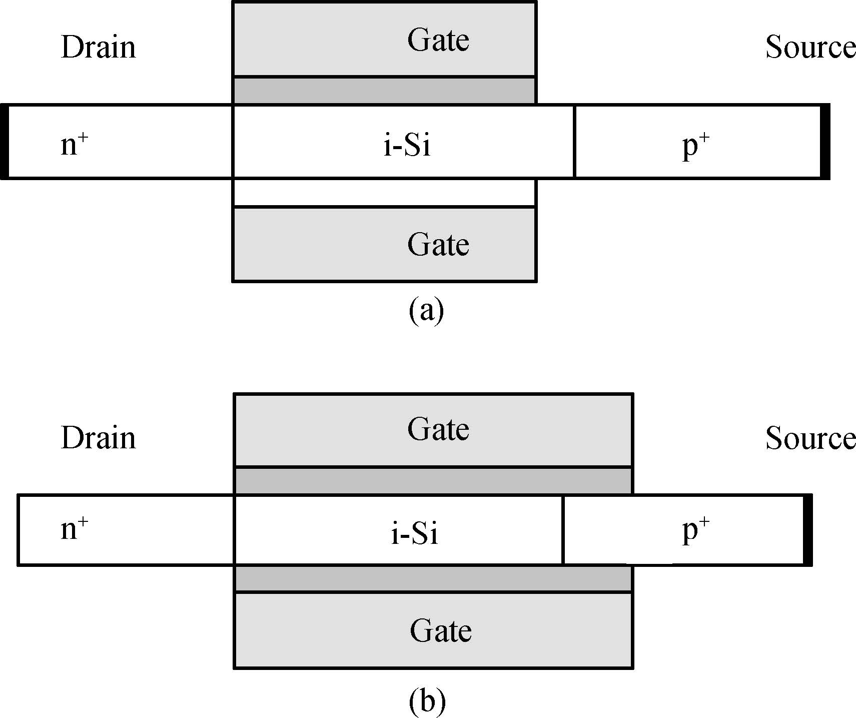
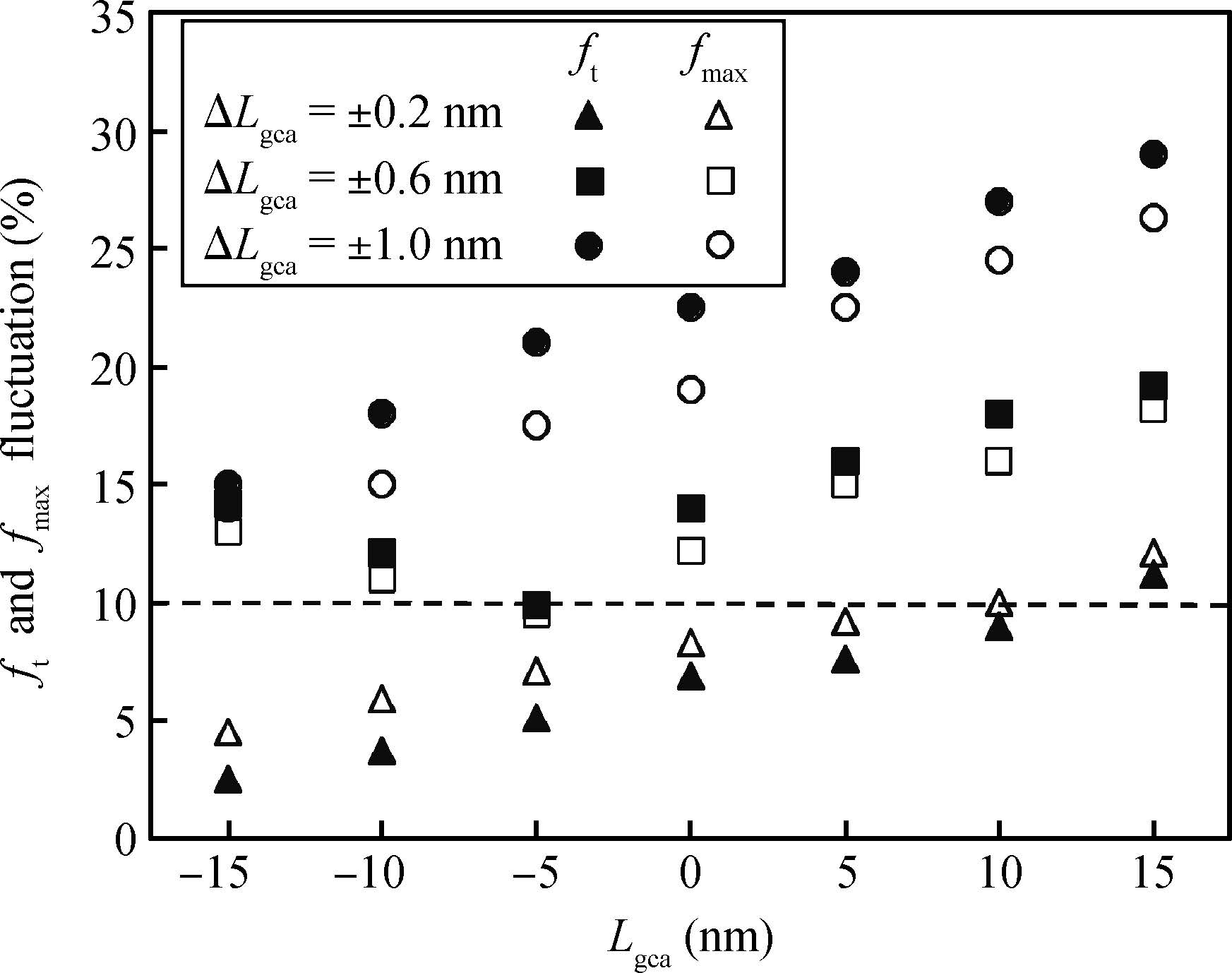
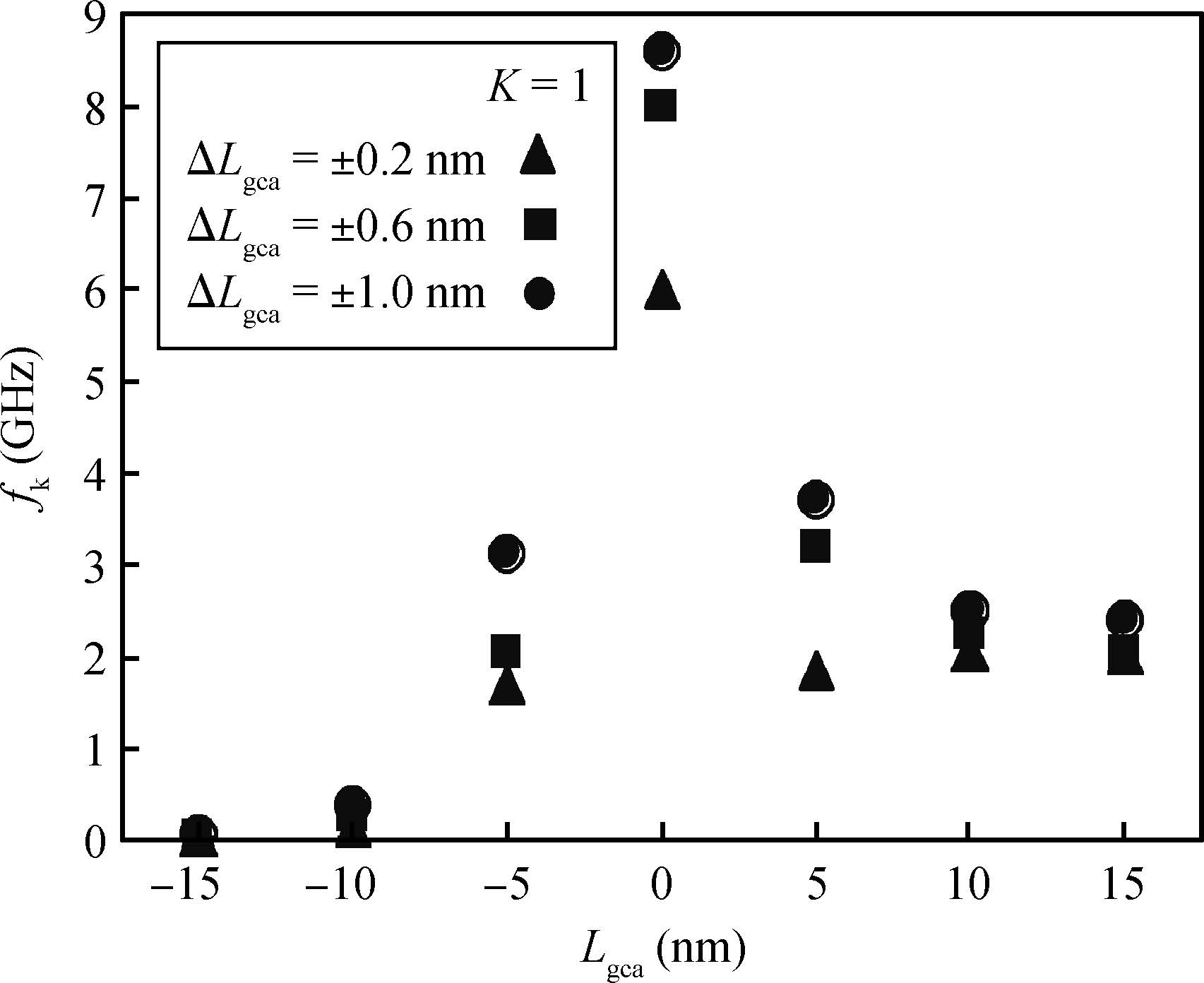
This paper presents the impact of parameter fluctuation due to process variation on radio frequency (RF) stability performance of double gate tunnel FET (DG TFET). The influence of parameter fluctuation due to process variation leads to DG TFET performance degradation. The RF figures of merit (FoM) such as cut-off frequency (ft), maximum oscillation frequency (fmax) along with stability factor for different silicon body thickness, gate oxide thickness and gate contact alignment are obtained from extracted device parameters through numerical simulation. The impact of parameter fluctuation of silicon body thickness, gate oxide thickness and gate contact alignment was found significant and the result provides design guidelines of DG TFET for RF applications.


J. Semicond.
2015, 36(8): 084002 doi: 10.1088/1674-4926/36/8/084002

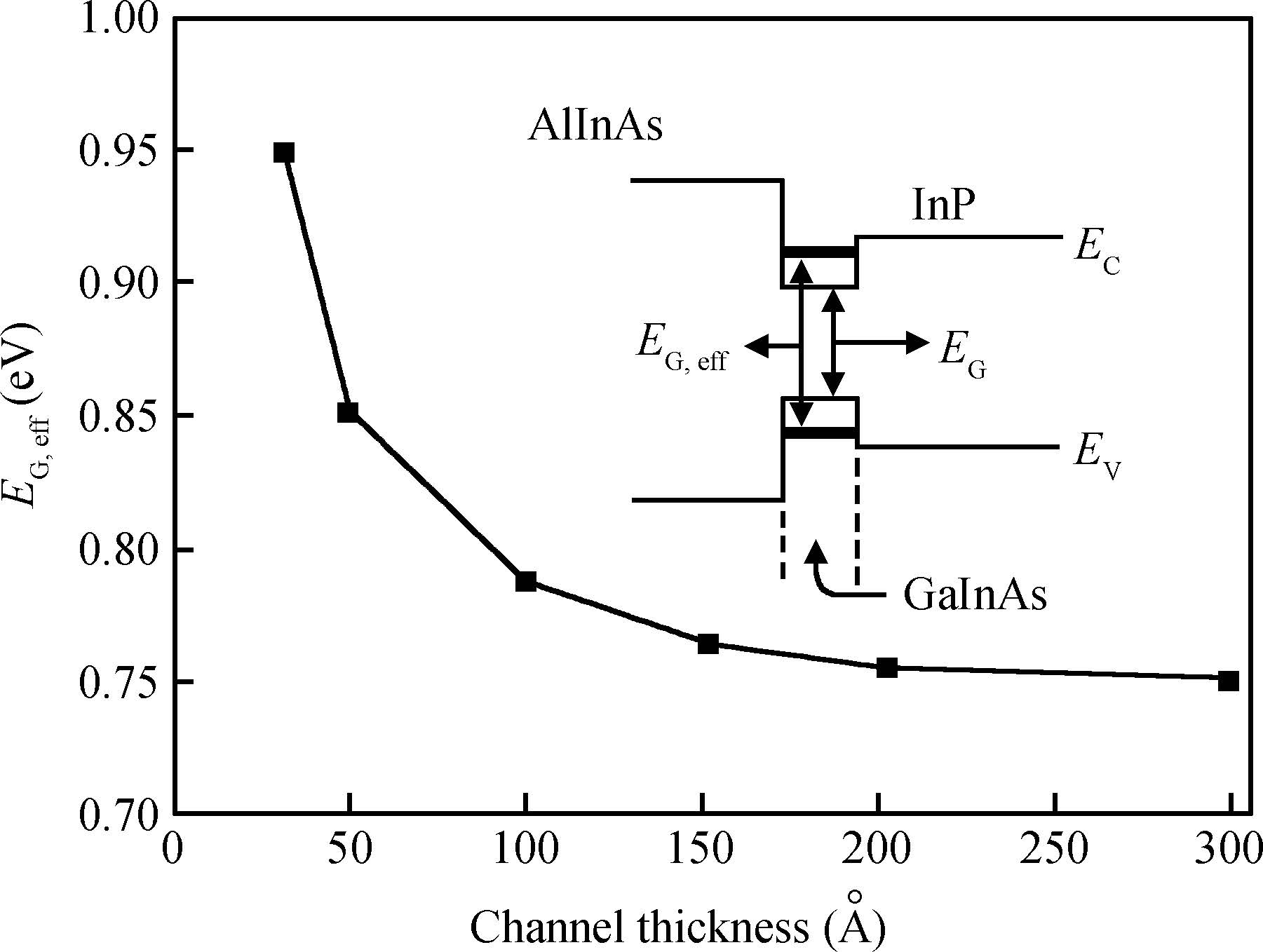
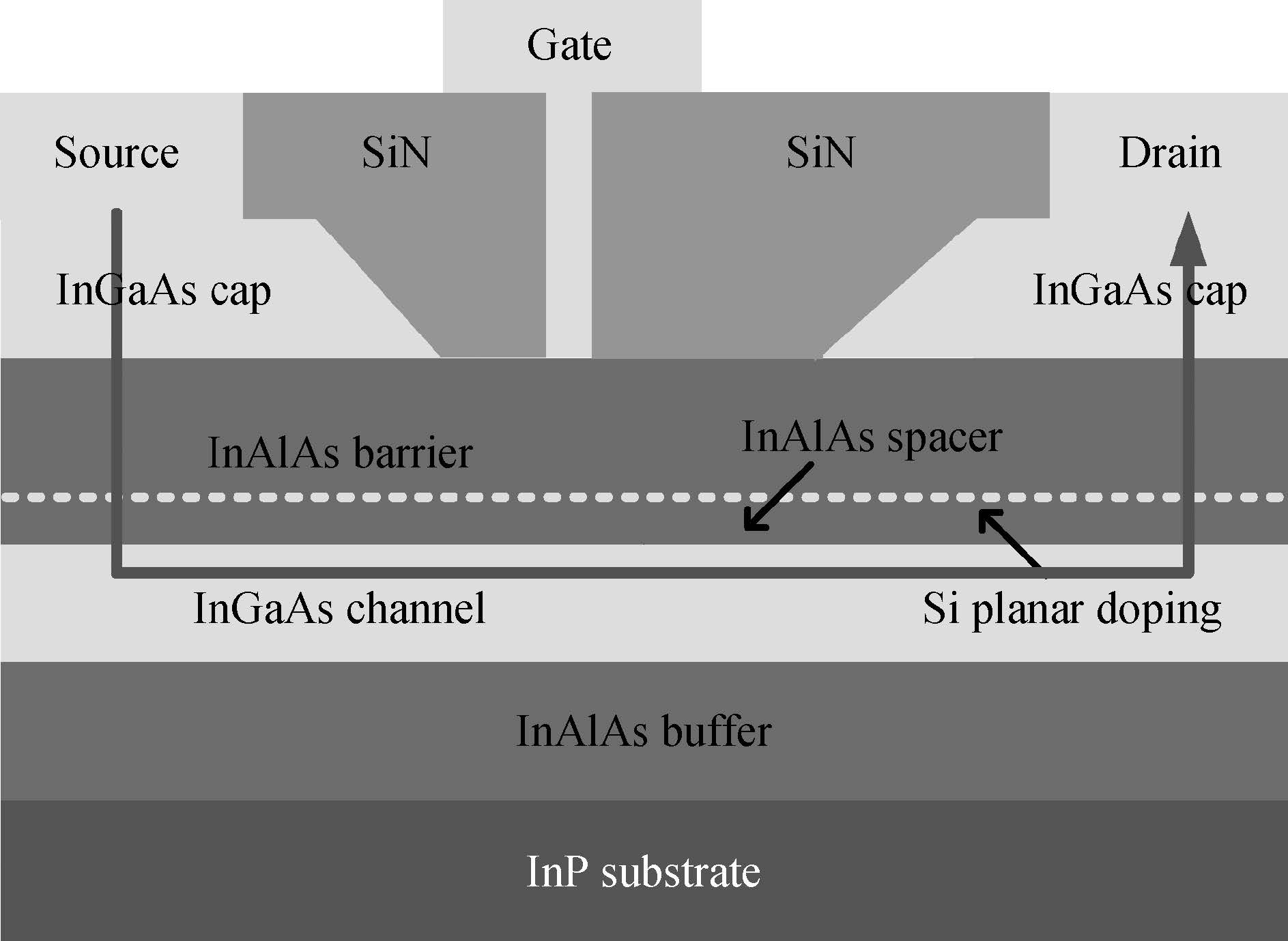
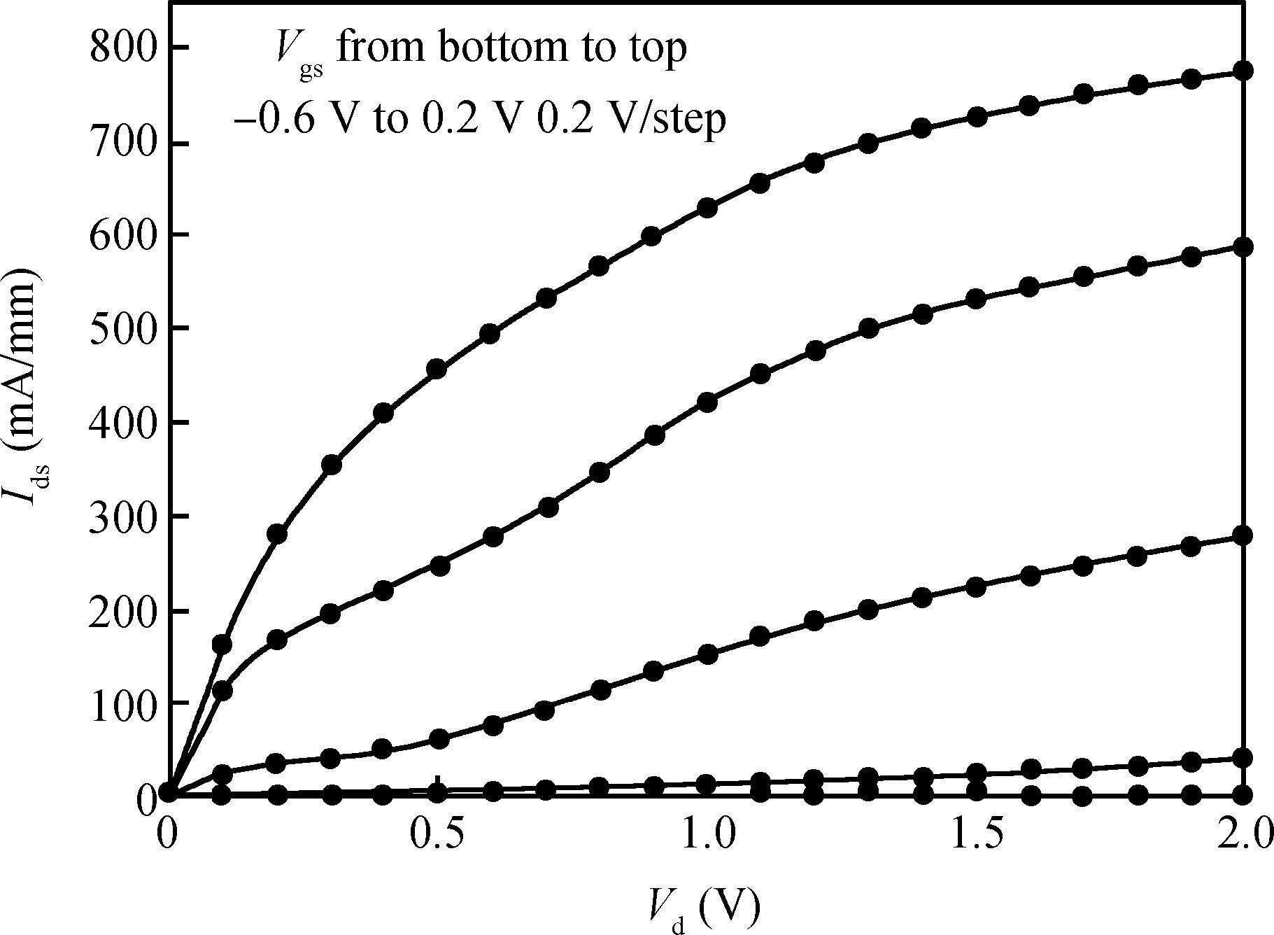
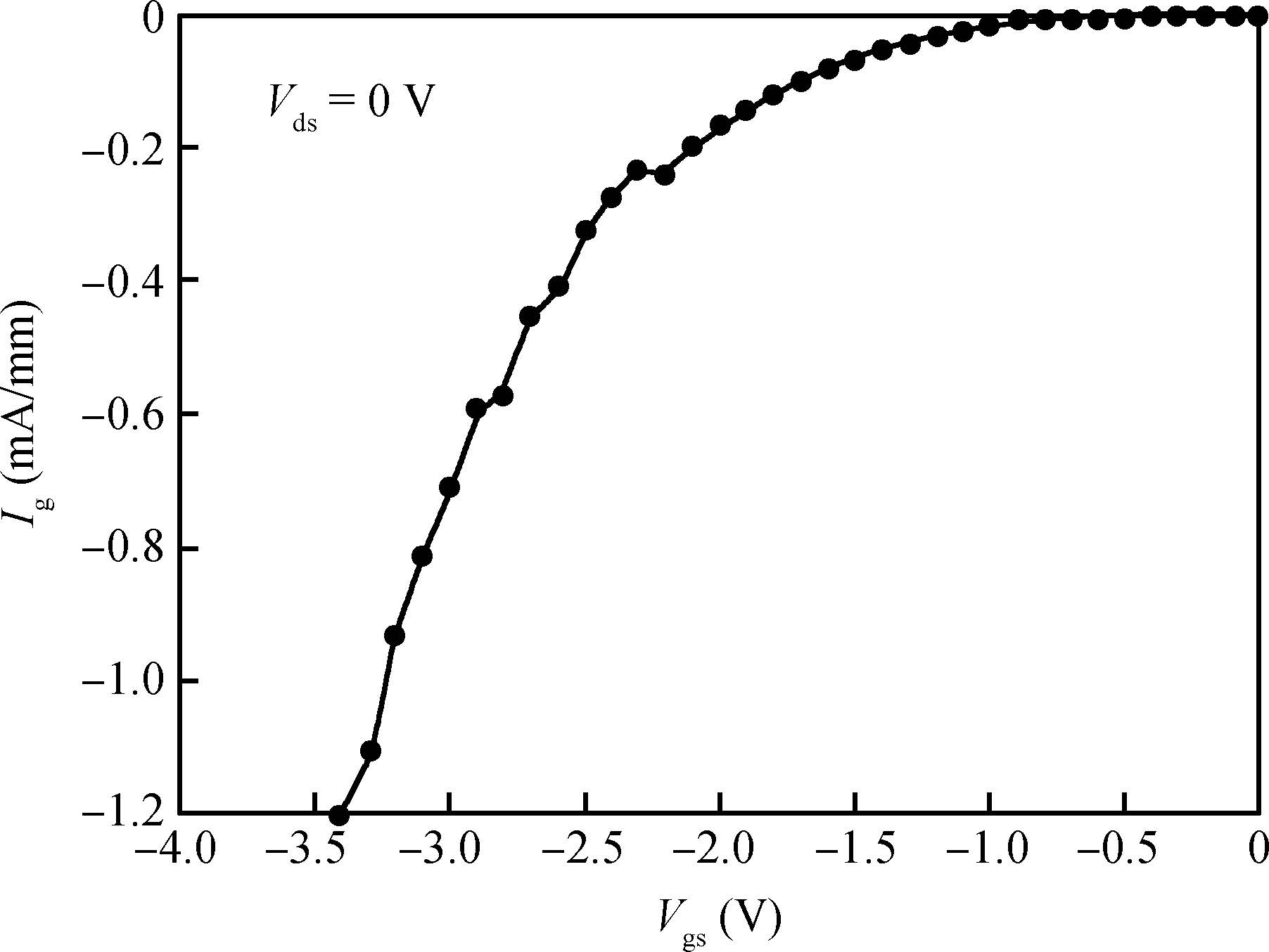
83-nm T-shaped gate InP-based In0.52Al0.48As/In0.65Ga0.35As pseudomorphic high electron mobility transistors (PHEMTs) with excellent DC and RF performance as well as low noise characteristics are reported, including a maximum saturation current density Idss of 894 mA/mm, a maximum extrinsic transconductance gm,max of 1640 mS/mm, an extrapolated cutoff frequency ft of 247 GHz and a maximum oscillation frequency fmax of 392 GHz which were based on the measured S-parameters from 1 to 110 GHz. The minimum noise figure (NFm min) measured by the cold-source method is 1 dB at 30 GHz associated with a gain of 14.5 dB at Vds of 0.8 V and Ids of 17 mA. These results were obtained by the combination of increased InAs mole fraction in the channel, gate size scaling, parasitic reduction and the quantization channel. These excellent results make it one of the most suitable devices for millimeter wave (MMW) low noise applications.


J. Semicond.
2015, 36(8): 084003 doi: 10.1088/1674-4926/36/8/084003

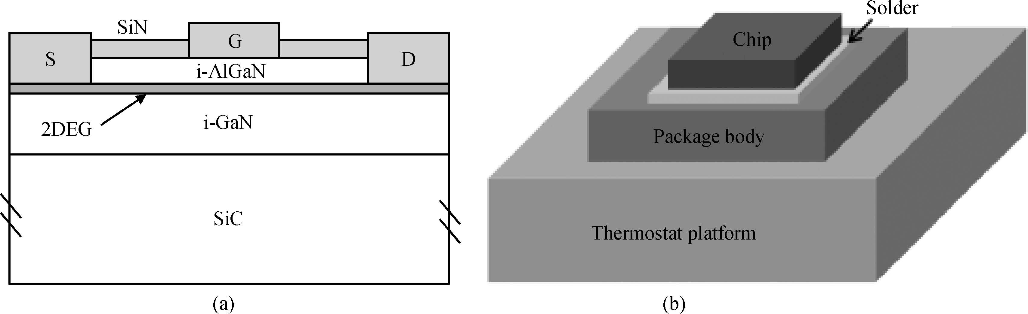
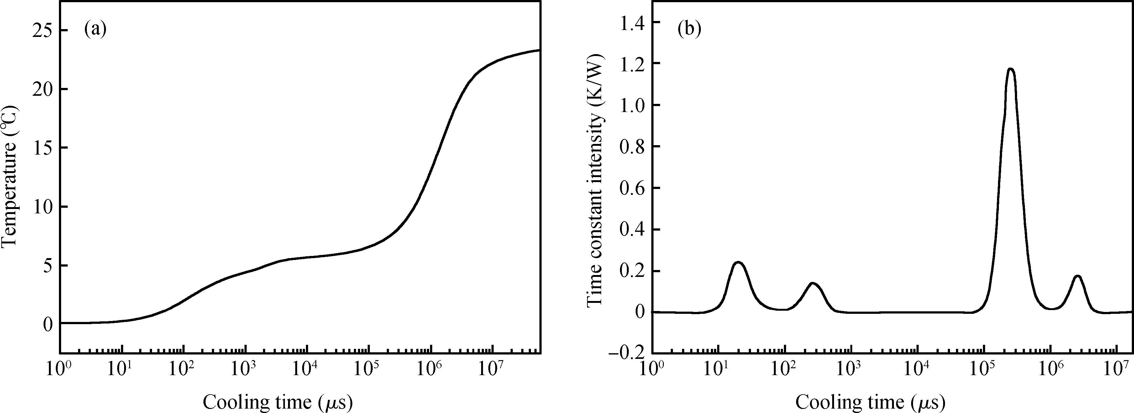
The transient temperature rise in the active region in AlGaN/GaN high electron mobility transistors (HEMTs) is measured using an electrical method. The original data are smoothed and denoised by a nonparametric fitting algorithm, called locally weighted scatterplot smoothing (LOWESS). The thermal time-constant spectrum is extracted to analyze the physical structure of the heat-conduction path in AlGaN/GaN HEMTs. The thermal time-constant spectra extracted using the LOWESS algorithm are richer and the RC network obtained is greater compared with those with the traditional denoising method (multi-exponential fitting). Thus, the analysis of the heat-flow path is more precise. The results show that the LOWESS nonparametric fitting algorithm can remove noise from measured data better than other methods and can retain the subtle variation tendency of the original discrete data. The thermal time-constant spectra extracted using this method can describe the subtle temperature variations in the AlGaN/GaN HEMT active region. This will help researchers to precisely analyze the layer composition of the heat-flow path.


J. Semicond.
2015, 36(8): 084004 doi: 10.1088/1674-4926/36/8/084004

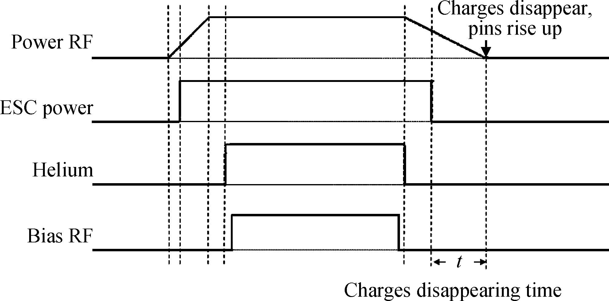
One of the core semiconductor devices is the electrostatic chuck. It has been widely used in plasma-based and vacuum-based semiconductor processing. The electrostatic chuck plays an important role in adsorbing and cooling/heating wafers, and has technical advantages on non-edge exclusion, high reliability, wafer planarity, particles reduction and so on. This article extracts key design elements from the existing knowledge and techniques of electrostatic chuck by the method proposed by Paul and Beitz, and establishes a design space systematically. The design space is composed of working objects, working principles and working structures. The working objects involve electrostatic chuck components and materials, classifications, and relevant properties; the working principles involve clamping force, residual force, and temperature control; the working structures describe how to compose an electrostatic chuck and to fulfill the overall functions. The systematic design space exhibits the main issues during electrostatic chuck design. The design space will facilitate and inspire designers to improve the design quality and shorten the design time in the conceptual design.


J. Semicond.
2015, 36(8): 084005 doi: 10.1088/1674-4926/36/8/084005

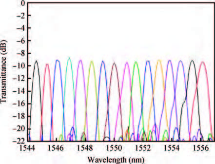
A 16-channel variable attenuator multiplexer/demultiplexer (VMUX) device is demonstrated. The VMUX is based on a rib-type structure on a silicon-on-insulator (SOI) platform. It consists of a 100-GHz arrayed waveguide grating (AWG) and an electro-optic variable optical attenuator (VOA) array with a p-i-n lateral diode structure. The insertion loss of the demonstrated device is about 9.1 dB and the corresponding crosstalk is about 10 dB. The injected current of the VOA is 60.74 mA at 20 dB attenuation and the whole area of the device is 2.9 × 1 mm2. The VMUX performs an excellent function of wavelength demultiplexing and optical power balancing in 16 channels.


J. Semicond.
2015, 36(8): 084006 doi: 10.1088/1674-4926/36/8/084006

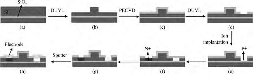
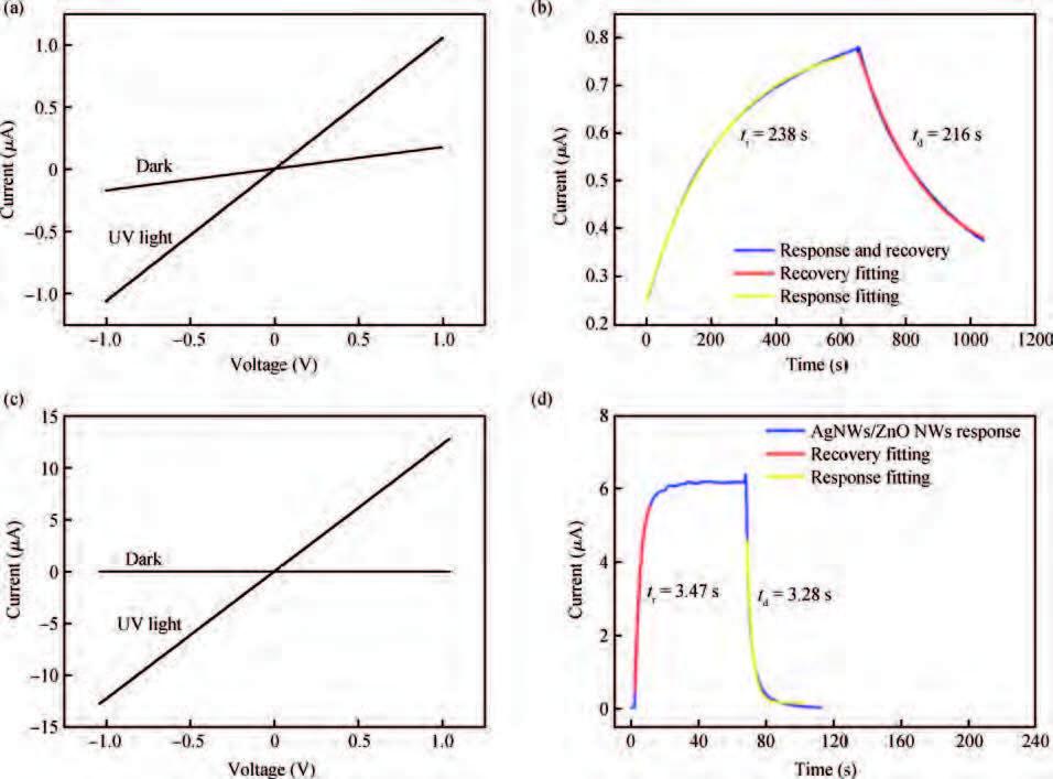
ZnO/Ag nanowires (NWs) film ultraviolet (UV) detector was fabricated by a simple and low-cost solution-processed method. In order to prepare this device, Ag NWs network was first spin-coated on glass substrate as a transparent conducting electrode, then ZnO NWs arrays were grown vertically on the Ag NWs network based on the hydrothermal method. This UV detector exhibited an excellent detection performance with large on/off ratio and short response time. Several process and working parameters were particularly investigated to analyze the relationship between structure and performance, which include growth time of ZnO NWs array, spin speed of Ag NWs network and working temperature. This UV photoconductive detector is based on two kinds of one-dimension nanomaterials, and it was regarded as a compromise between high performance with large area, low voltage and low cost.


An inherent curvature-compensated voltage reference using non-linearity of gate coupling coefficient
J. Semicond.
2015, 36(8): 085001 doi: 10.1088/1674-4926/36/8/085001

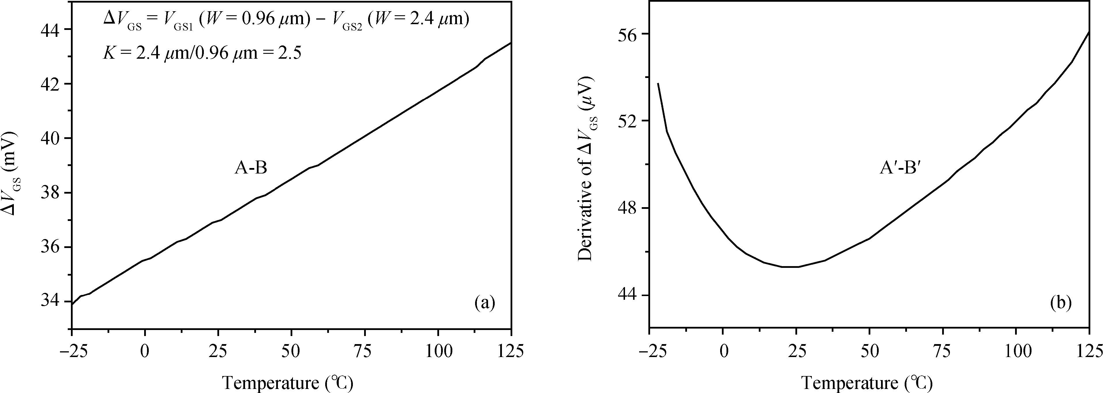
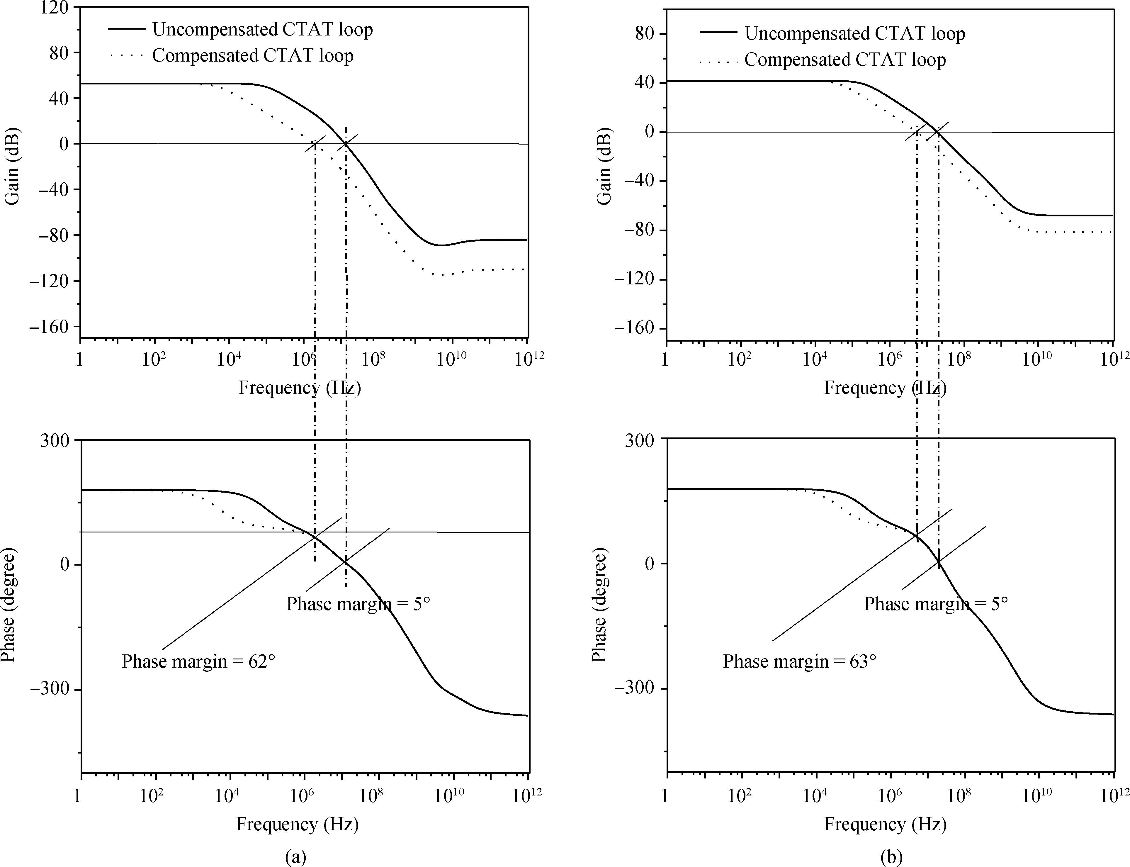
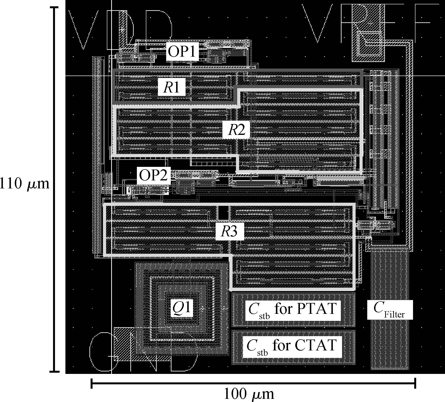
A novel current-mode voltage reference circuit which is capable of generating sub-1 V output voltage is presented. The proposed architecture exhibits the inherent curvature compensation ability. The curvature compensation is achieved by utilizing the non-linear behavior of gate coupling coefficient to compensate non-linear temperature dependence of base-emitter voltage. We have also utilized the developments in CMOS process to reduce power and area consumption. The proposed voltage reference is analyzed theoretically and compared with other existing methods. The circuit is designed and simulated in 180 nm mixed-mode CMOS UMC technology which gives a reference level of 246 mV. The minimum required supply voltage is 1 V with maximum current drawn of 9.24 μA. A temperature coefficient of 9 ppm/℃ is achieved over -25 to 125 ℃ temperature range. The reference voltage varies by ±11 mV across process corners. The reference circuit shows the line sensitivity of 0.9 mV/V with area consumption of 100 × 110 μm2.


J. Semicond.
2015, 36(8): 085002 doi: 10.1088/1674-4926/36/8/085002

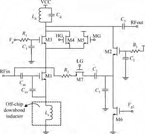
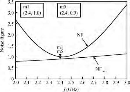
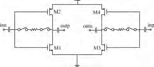
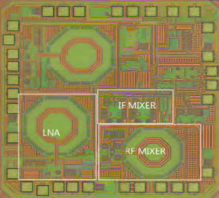
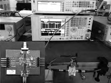
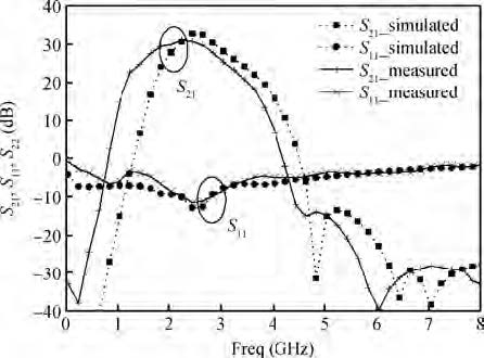
This paper describes the implementation of an RF receiver front-end for the 2.4 GHz industrial scientific medical band under TSMC 0.13μm CMOS technology; it comprises a low noise amplifier (LNA) which uses an added gate-source capacitor for low power performance and a dual-converter composed of a single-balanced active RF mixer and double-balanced passive IF mixer. Dual-down-conversion technique is used for reducing power. A 2.4 GHz low power low-IF RF receiver front-end is proposed. An LNA for rejecting image signal, an inductor-capacitor (LC) tank is used in series with source of input-stage transistor of the RF mixer, and combined with the LC load of the LNA, 30-dB image rejection is realized. Fabricated in a 0.13μm CMOS process, the proposed chip occupies 0.42 mm2 area, achieves 4 dB noise figure, -22 dBm IIP3 and 37 dB voltage gain dissipating only 4.2-mW under 1.2-V supply.


J. Semicond.
2015, 36(8): 085003 doi: 10.1088/1674-4926/36/8/085003

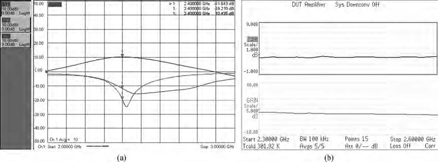
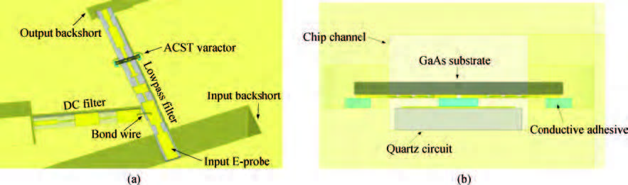
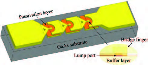
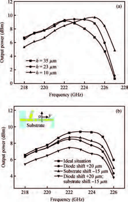
A frequency-multiplied source at the terahertz band using discrete planar Schottky diodes, which is a critical element in heterodyne instruments, has been studied by some domestic research institutions in recent years. Besides the design method, there are still many crucial problems that must be taken into consideration in the design. This article mainly discuss three aspects based on the measured data of a 225 GHz tripler that we designed. Firstly, the accuracy of the diode model concerns the reliability of the simulation results. According to the Spice parameters and the measured results, the physical size and the DC parameter of the Schottky diode can be corrected until there is a good consistency between the simulated and measured results. Secondly, the heat accumulation happens to the Schottky junction when the high input power is added. A steady-state thermal simulation is done and the results show that the hottest temperature is about 140 ℃ with 250 mW input power, which is safe to the diode. Lastly, some non-ideal factors are brought during the assembly process such as the uncertainty in the conductive adhesive shape and location deviation of the circuit. Furthermore, the effect on the performance of the frequency multiplier is calculated in this work.


J. Semicond.
2015, 36(8): 085004 doi: 10.1088/1674-4926/36/8/085004

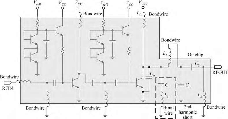
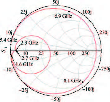
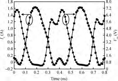
A broadband class-F power amplifier for multiband LTE handsets applications is developed across 2.3-2.7 GHz. The power amplifier maintains constant fundamental impedance at the output matching circuit which is operating for broadband. The nearly zero of second harmonic impedance and nearly infinity of third harmonic impedance are found for highly efficient class-F PA. The harmonic control circuits are immersed into the broadband output matching for fundamental frequency. For demonstration, the PA is implemented in InGaP/GaAs HBT process, and tested across the frequency range of 2.3-2.7 GHz using a long-term evolution signal. The presented PA delivers good performance of high efficiency and high linearity, which shows that the broadband class-F PA supports the multiband LTE handsets applications.


J. Semicond.
2015, 36(8): 085005 doi: 10.1088/1674-4926/36/8/085005

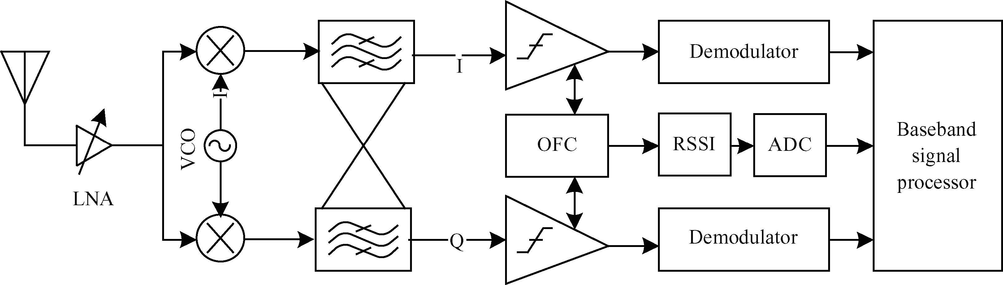
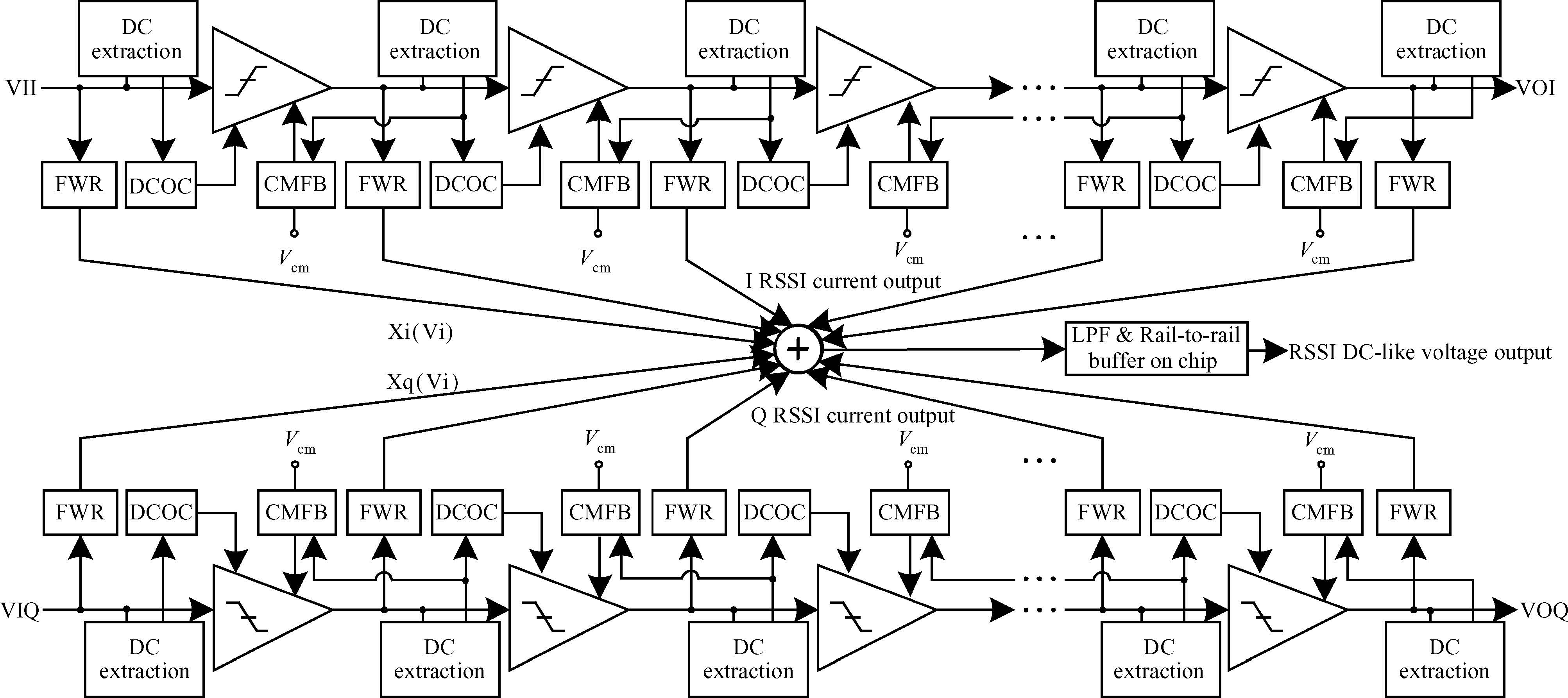
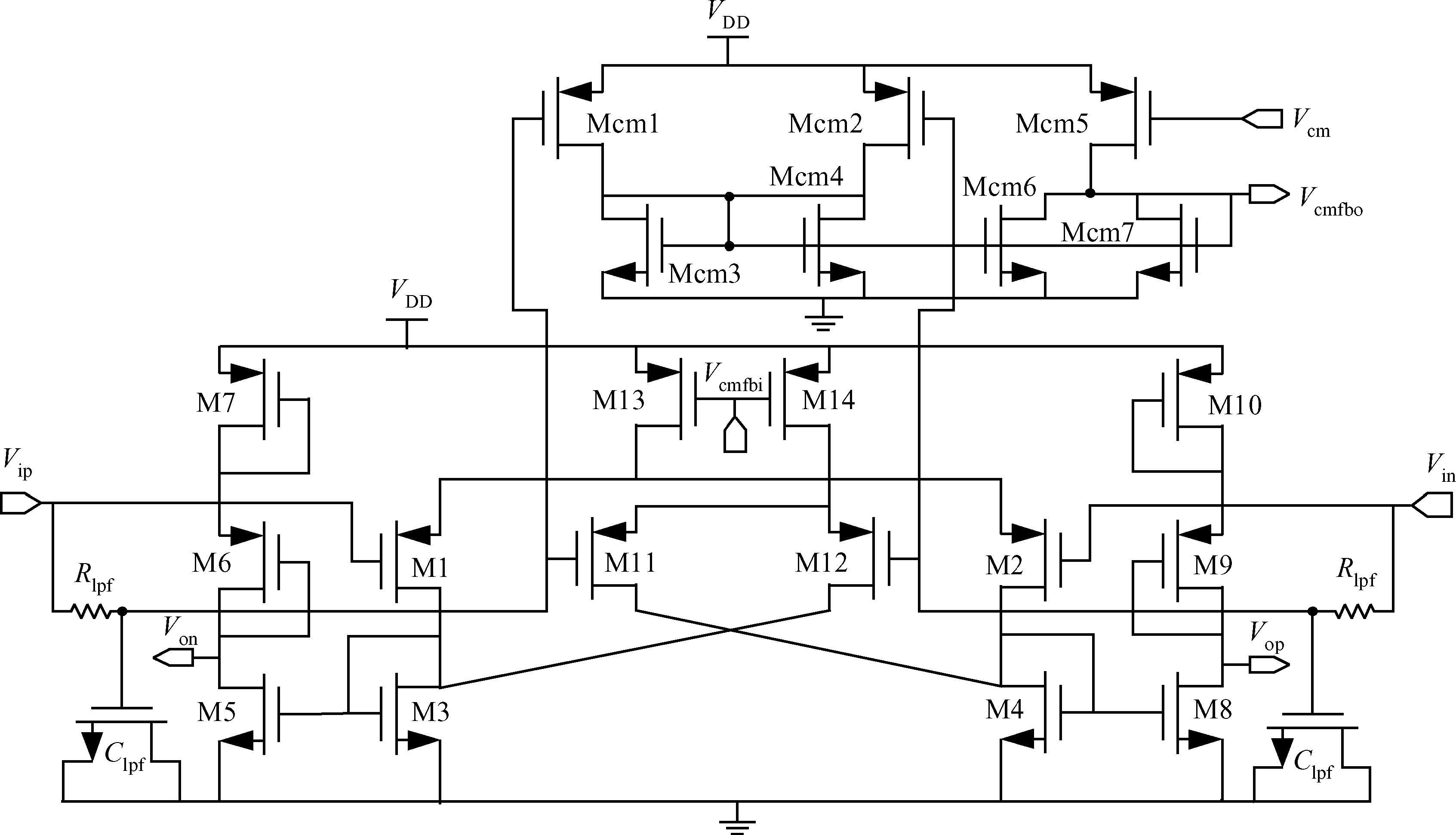
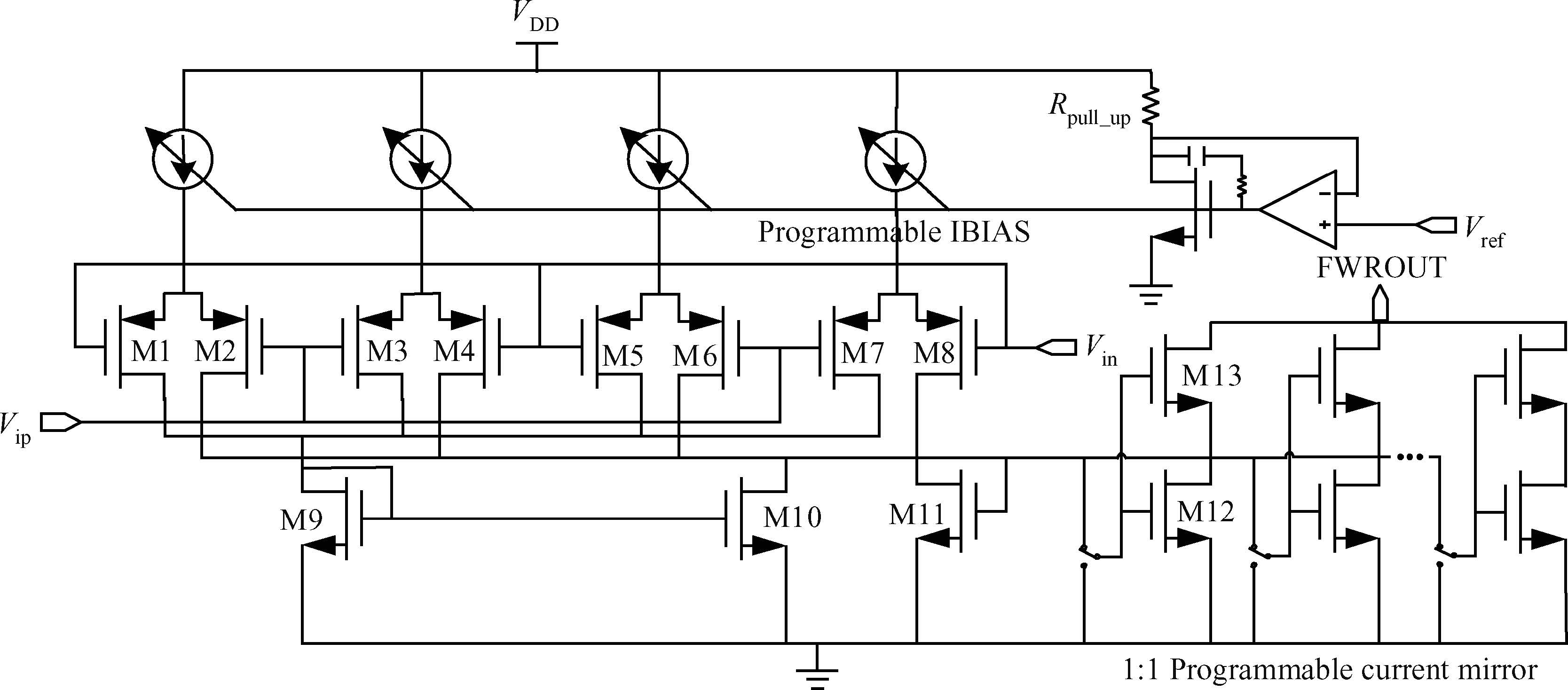
This paper presents a high resolution, process/temperature variation tolerant received signal strength indicator (RSSI) for wireless networks for industrial automation process automation (WIA-PA) transceiver fabricated in 0.18μm CMOS technology. The active area of the RSSI is 0.24 mm2. Measurement results show that the proposed RSSI has a dynamic range more than 70 dB and the linearity error is within ± 0.5 dB for an input power from -70 to 0 dBm (dBm to 50 Ω ), the corresponding output voltage is from 0.81 to 1.657 V and the RSSI slope is 12.1 mV/dB while consuming all of 2 mA from a 1.8 V power supply. Furthermore, by the help of the integrated compensation circuit, the proposed RSSI shows the temperature error within ± 1.5 dB from -40 to 85 ℃, and process variation error within ± 0.25 dB, which exhibits good temperature-independence and excellent robustness against process variation characteristics.


J. Semicond.
2015, 36(8): 085006 doi: 10.1088/1674-4926/36/8/085006

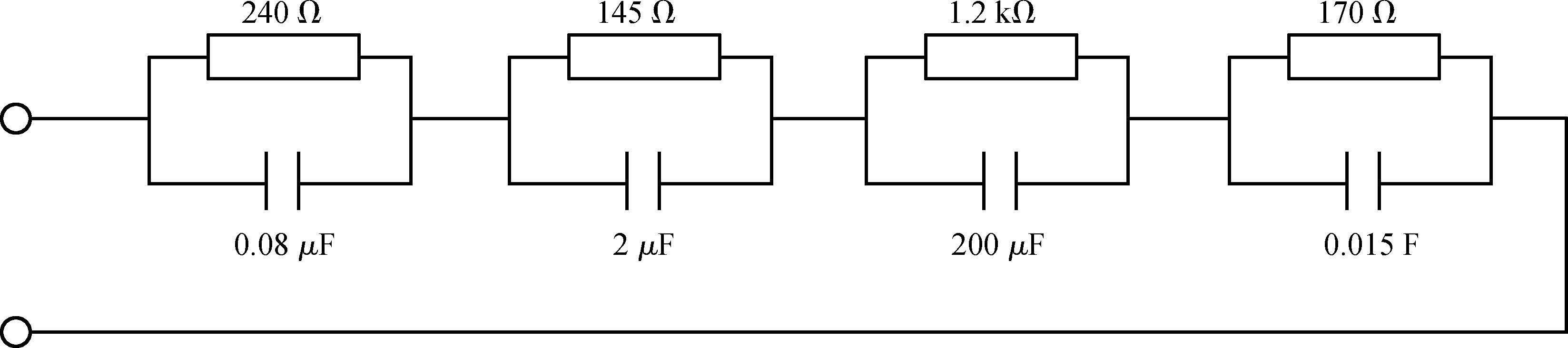
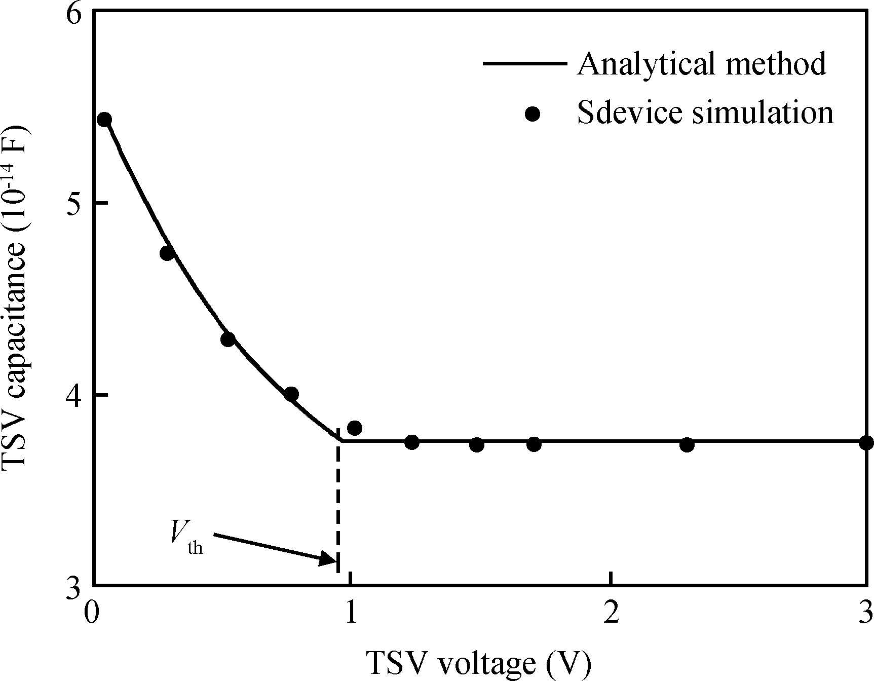
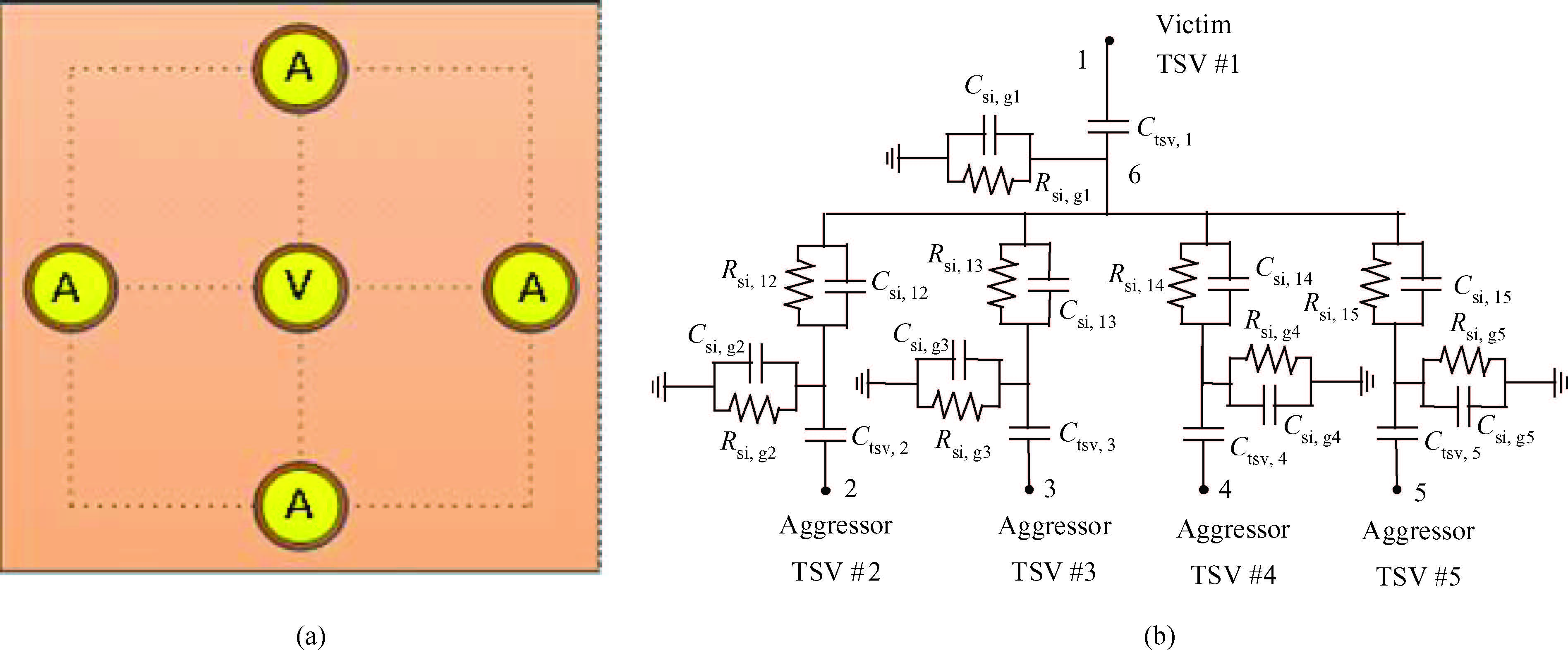
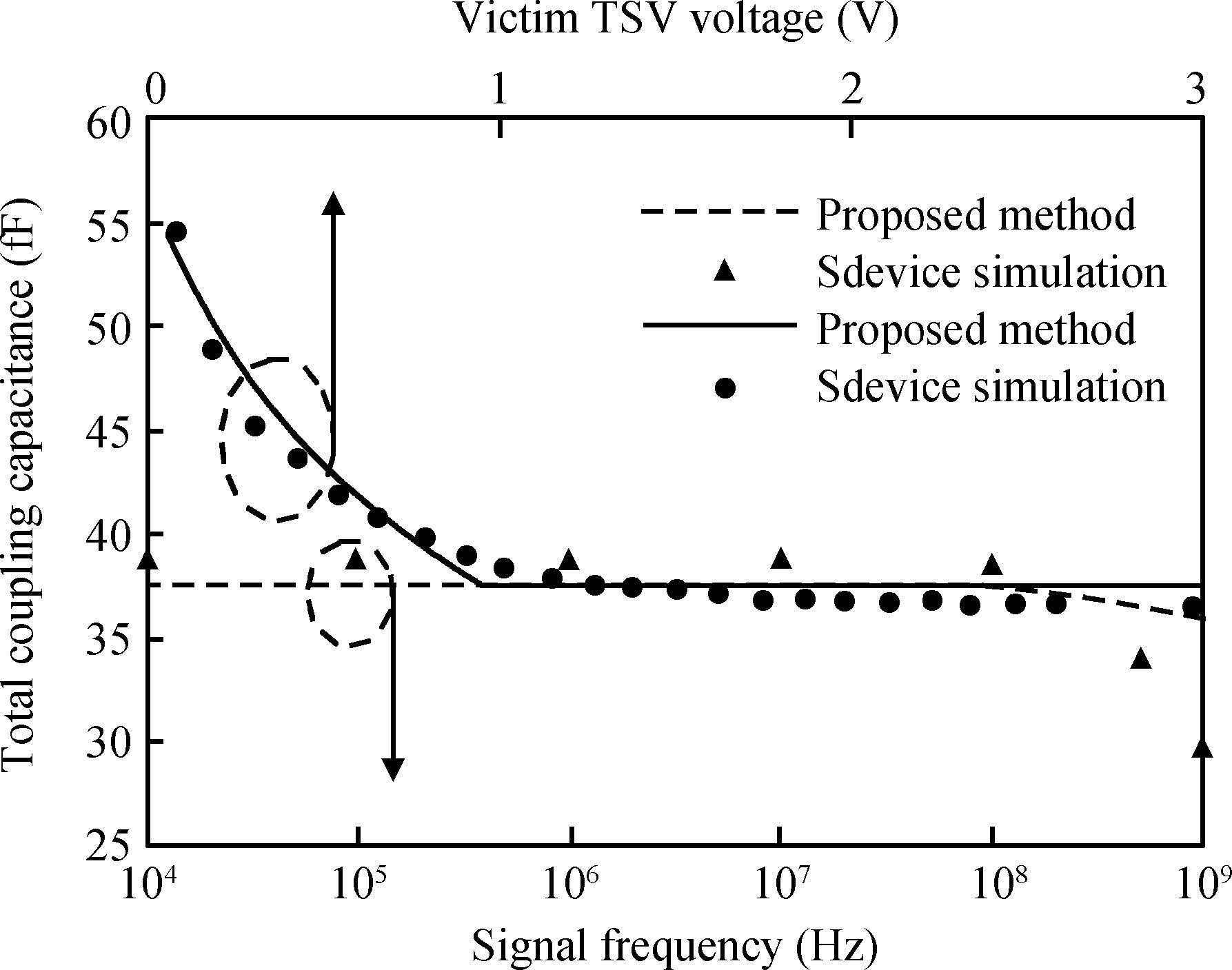
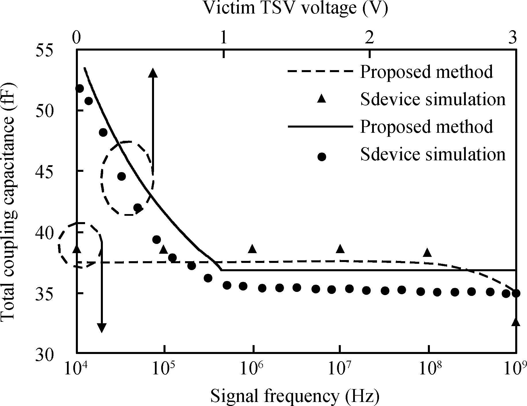
To build an accurate electric model for through-silicon vias (TSVs) in 3D integrated circuits (ICs), a resistance and capacitance (RC) circuit model and related efficient extraction technique are proposed. The circuit model takes both semiconductor and electrostatic effects into account, and is valid for low and medium signal frequencies. The electrostatic capacitances are extracted with a floating random walk based algorithm, and are then combined with the voltage-dependent semiconductor capacitances to form the equivalent circuit. Compared with the method used in Synopsys's Sdevice, which completely simulates the electro/semiconductor effects, the proposed method is more efficient and is able to handle the general TSV layout as well. For several TSV structures, the experimental results validate the accuracy of the proposed method for the frequency range from 10 kHz to 1 GHz. The proposed method demonstrated 47× speedup over the Sdevice for the largest 9-TSV case.


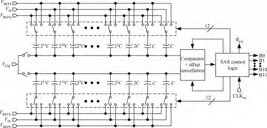
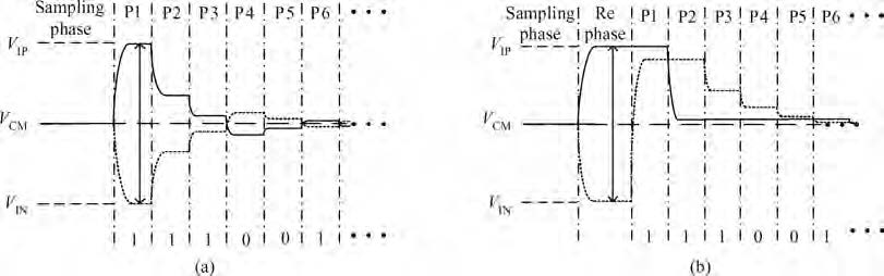
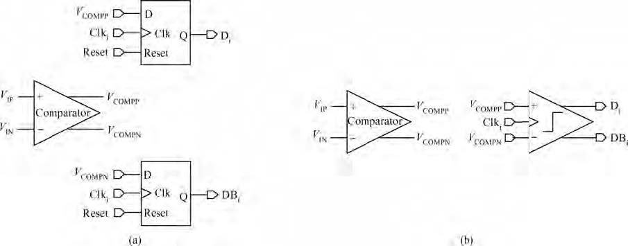
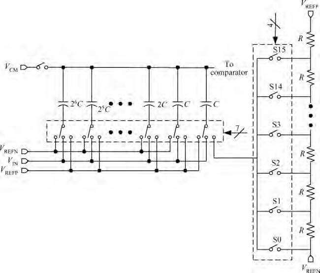
A low power 12-bit 1 Msps successive approximation register ADC with an improved switching procedure
J. Semicond.
2015, 36(8): 085007 doi: 10.1088/1674-4926/36/8/085007

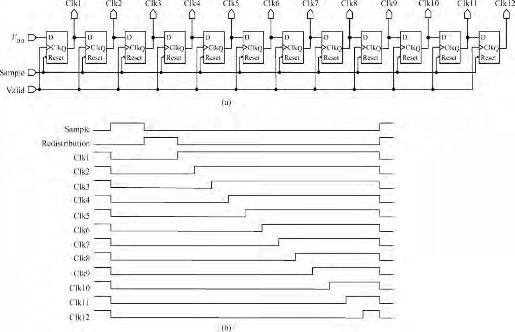
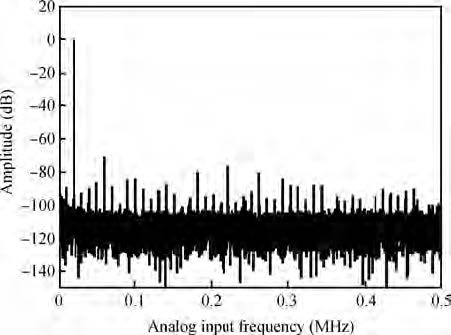
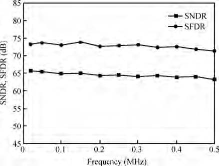
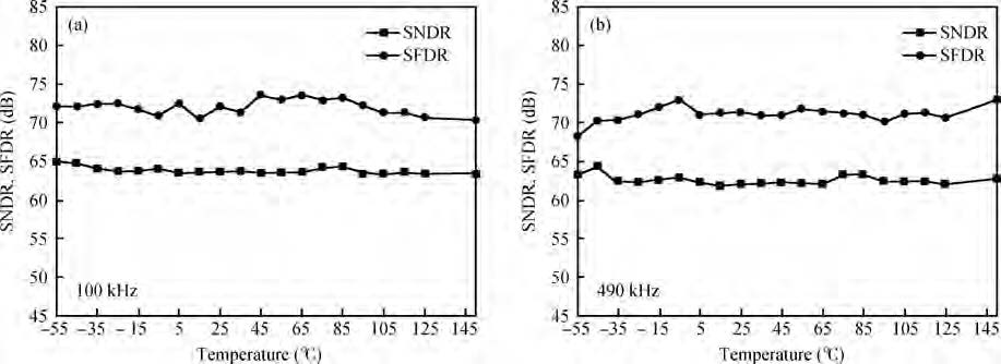
As a key building block of data acquisition systems, power dissipation of the successive approximation register (SAR) ADC determines the total power consumption of the system. In this paper, a low power 12-bit 1 Msps SAR ADC with an improved switching procedure is presented. Power consumption and area occupation could be significantly reduced by using the proposed switching procedure. Compared to converters that use the conventional switching procedure, the average switching energy could be reduced by about 80% and the total capacitance could be reduced by 50%. A simplified digital control logic is utilized to reduce power dissipation and area occupation of the digital control circuits. Simulation results show that the power dissipated by the proposed digital control circuits could be reduced by about 50% compared to the power dissipated by conventional control circuits. The chip has been processed in a standard 0.35μm CMOS technology and has a core die area of 1.12 mm2. A signal-to-noise-and-distortion-ratio of 64.2 dB has been measured with a 100 kHz signal input under a wide range variation of temperature from -55 to 150 ℃. The total power consumption of the prototype is only 0.72 mW with a 3.3 V supply voltage.


J. Semicond.
2015, 36(8): 085008 doi: 10.1088/1674-4926/36/8/085008

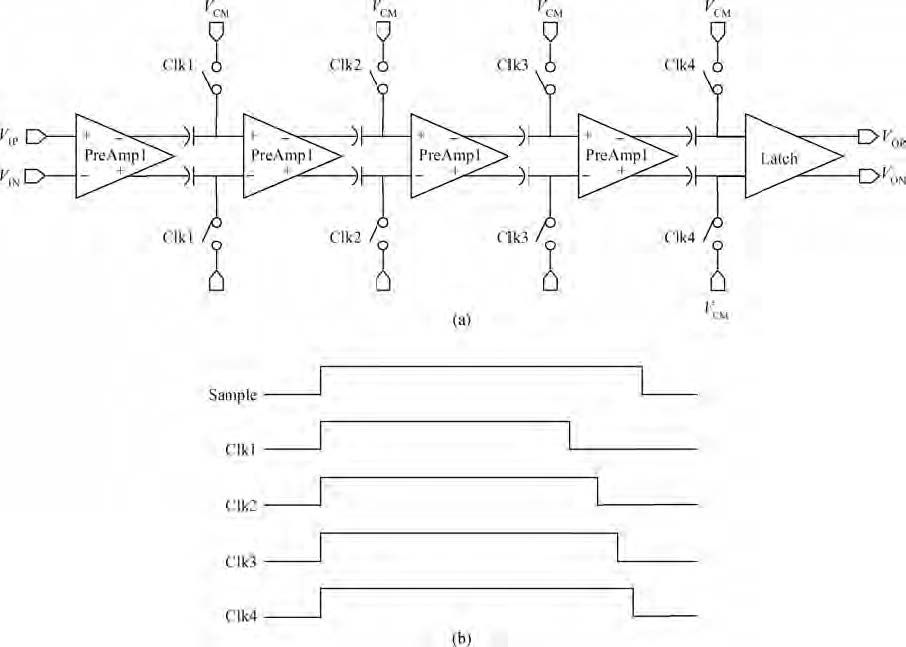
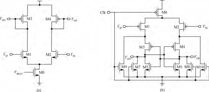
A 10 bit, 120 MS/s two-channel pipelined analog-to digital converter (ADC) is presented. The ADC is featured with improved switch by using the body effect to improve its conduction performance. A scaling down strategy is proposed to get more efficiency in the OTA's layout design. Implemented in a 0.18-μ m CMOS technology, the ADC's prototype occupied an area of 2.05 × 1.83 mm2. With a sampling rate of 120-MS/s and an input of 4.9 MHz, the ADC achieves a spurious-free-dynamic range of 74.32 dB and signal-to-noise-and-distortion ratio of 55.34 dB, while consuming 220-mW/channel at 3-V supply.


J. Semicond.
2015, 36(8): 085009 doi: 10.1088/1674-4926/36/8/085009

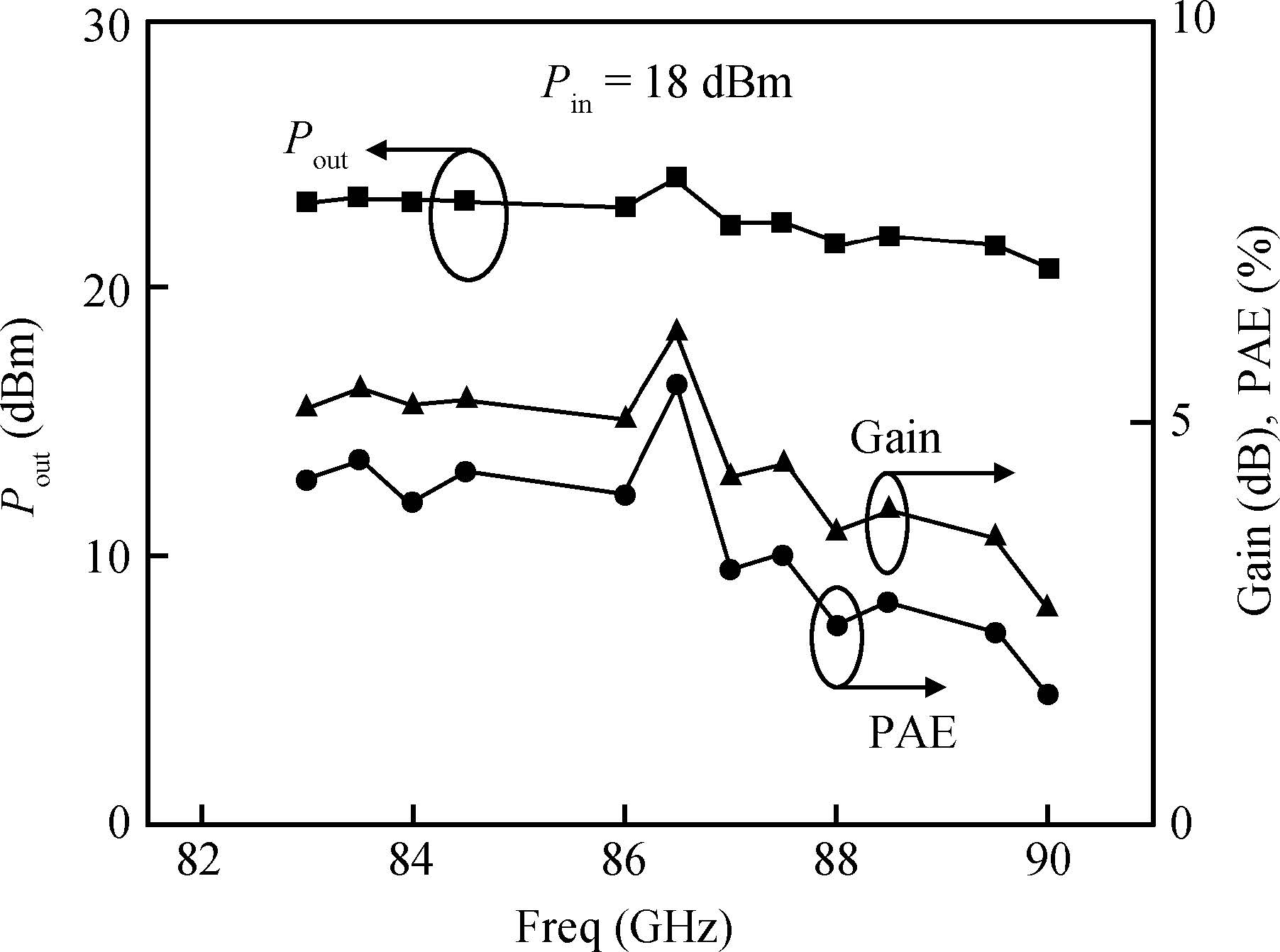
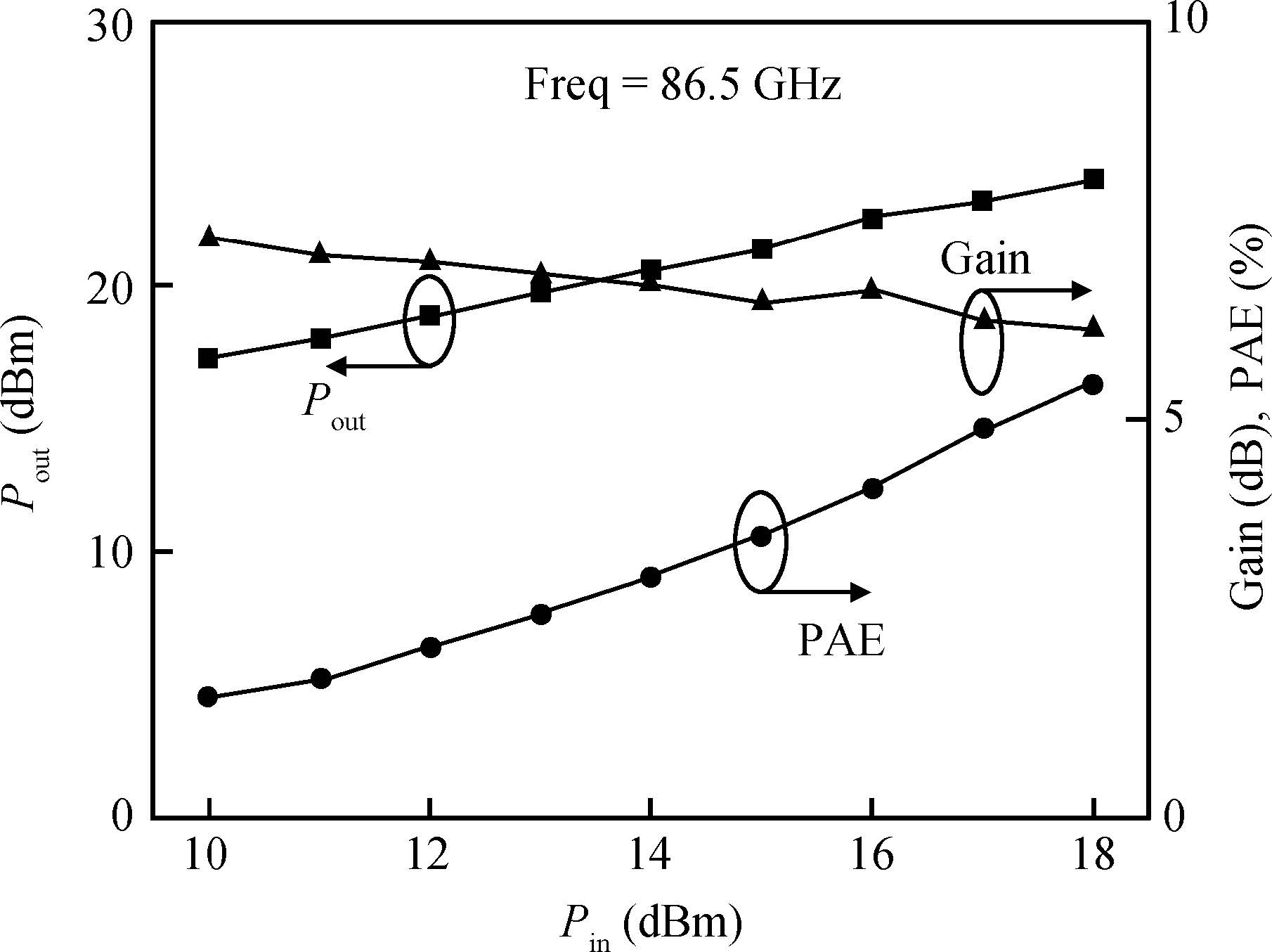
A three-stage W-band GaN monolithic microwave integrated circuit power amplifier (MMIC PA) is reported. In order to manage coupling effects between all the parts of the W-band MMIC, all matching and bias networks have been first optimized using circuit simulating software and then systematically simulated on 3D full-wave electromagnetic simulator. The fabricated MMIC PA achieves a 257 mW output power at 86.5 GHz in continuous-wave mode, with an associated power added efficiency of 5.4% and an associated power gain of 6.1 dB. The power density is 459 mW/mm. Moreover, the MMIC PA offers over 100 mW in the 83-90 GHz bandwidth. Those performances were measured at drain bias of 12 V.


J. Semicond.
2015, 36(8): 086001 doi: 10.1088/1674-4926/36/8/086001

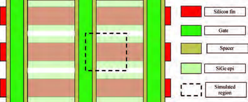
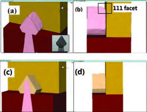
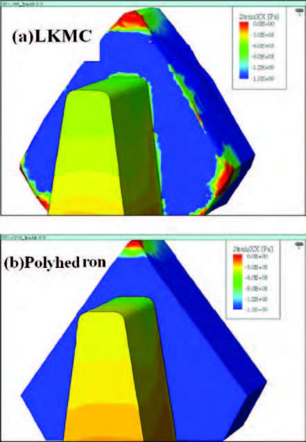
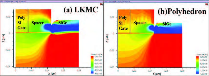
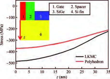
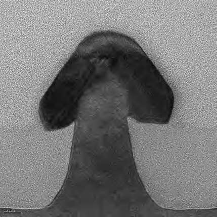
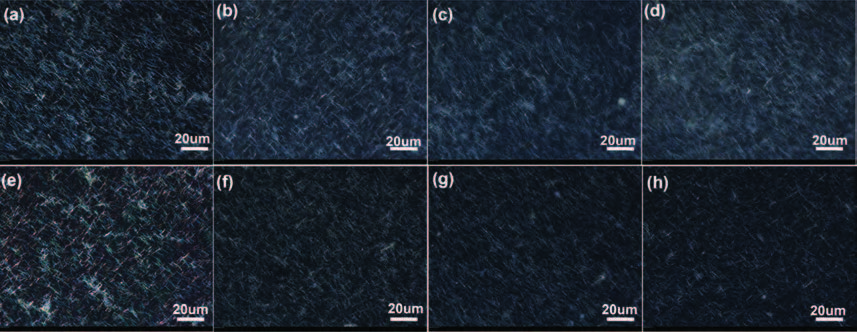
A new simulation method and test instrument has been adopted to verify the traditional stress simulation in FinFET. First, a new algorithm named lattice kinetic Monte Carlo (LKMC) is used to simulate the SiGe epitaxy in source/drain regions and the stress distribution is consequently extracted after the LKMC simulation. Systematic comparison between the traditional polyhedron method and the LKMC method is carried out. The results confirm that extracted stress from both methods is consistent, which verifies the validity of traditional polyhedron method for the purpose of simulating stress in FinFET. In the following experiment, p-type FinFETs with SiGe stressors in source/drain regions are fabricated. The nano beam diffraction (NBD) method is employed to characterize the strain in Si fin. The strain value from the NBD test agrees well with the value extracted from traditional polyhedron simulation.