Issue Browser
Volume 38, Issue 10,
Oct 2017
J. Semicond.
2017, 38(10): 105001 doi: 10.1088/1674-4926/38/10/105001

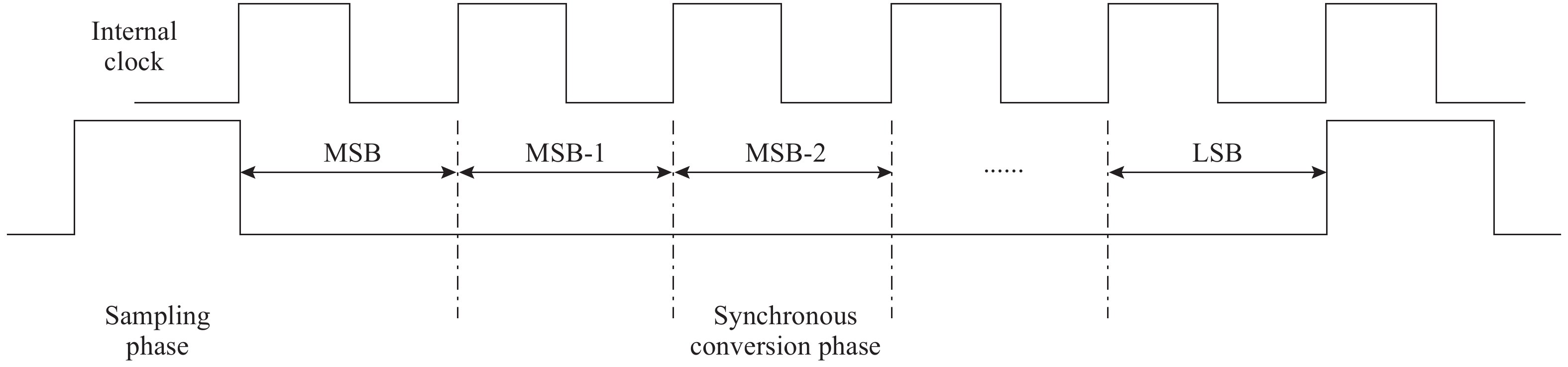
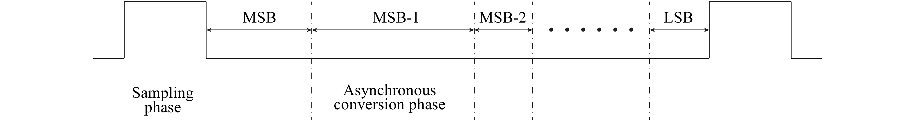
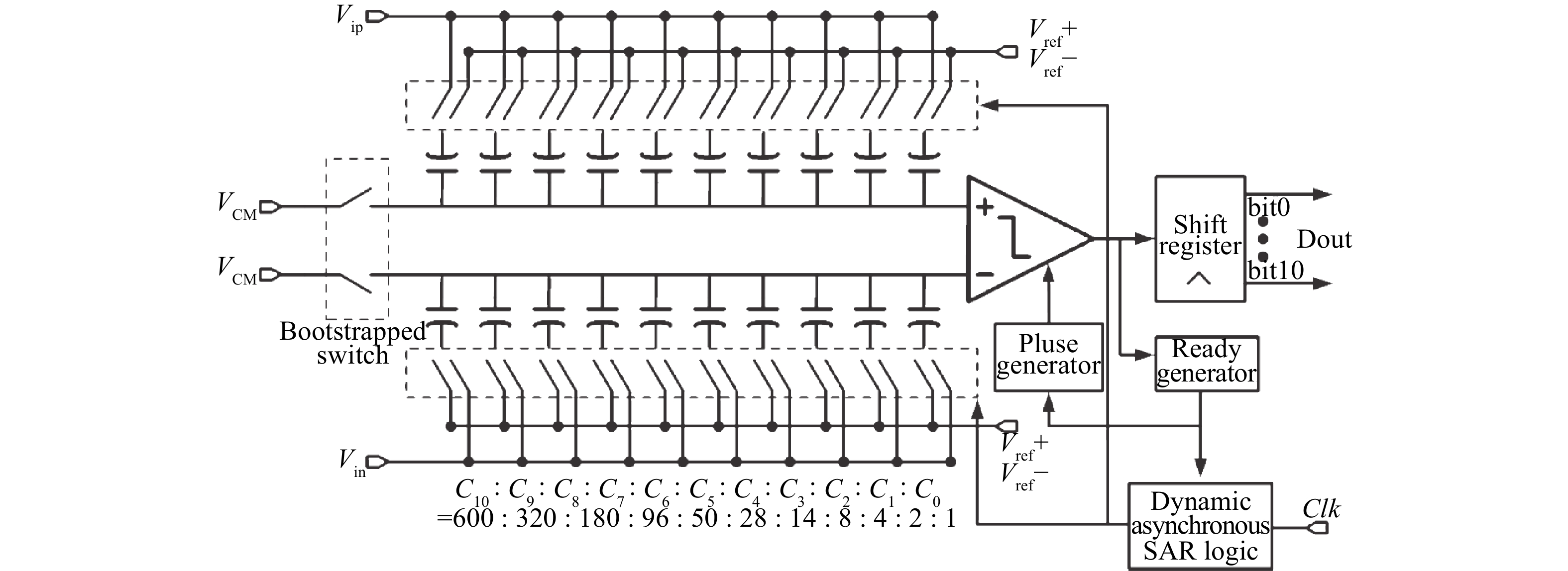
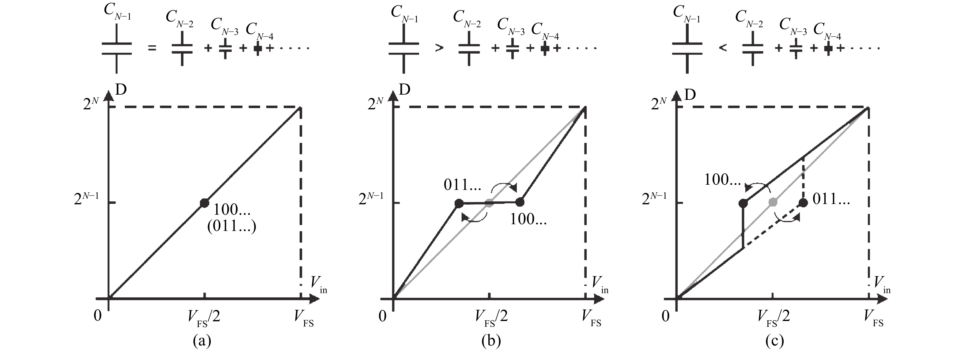
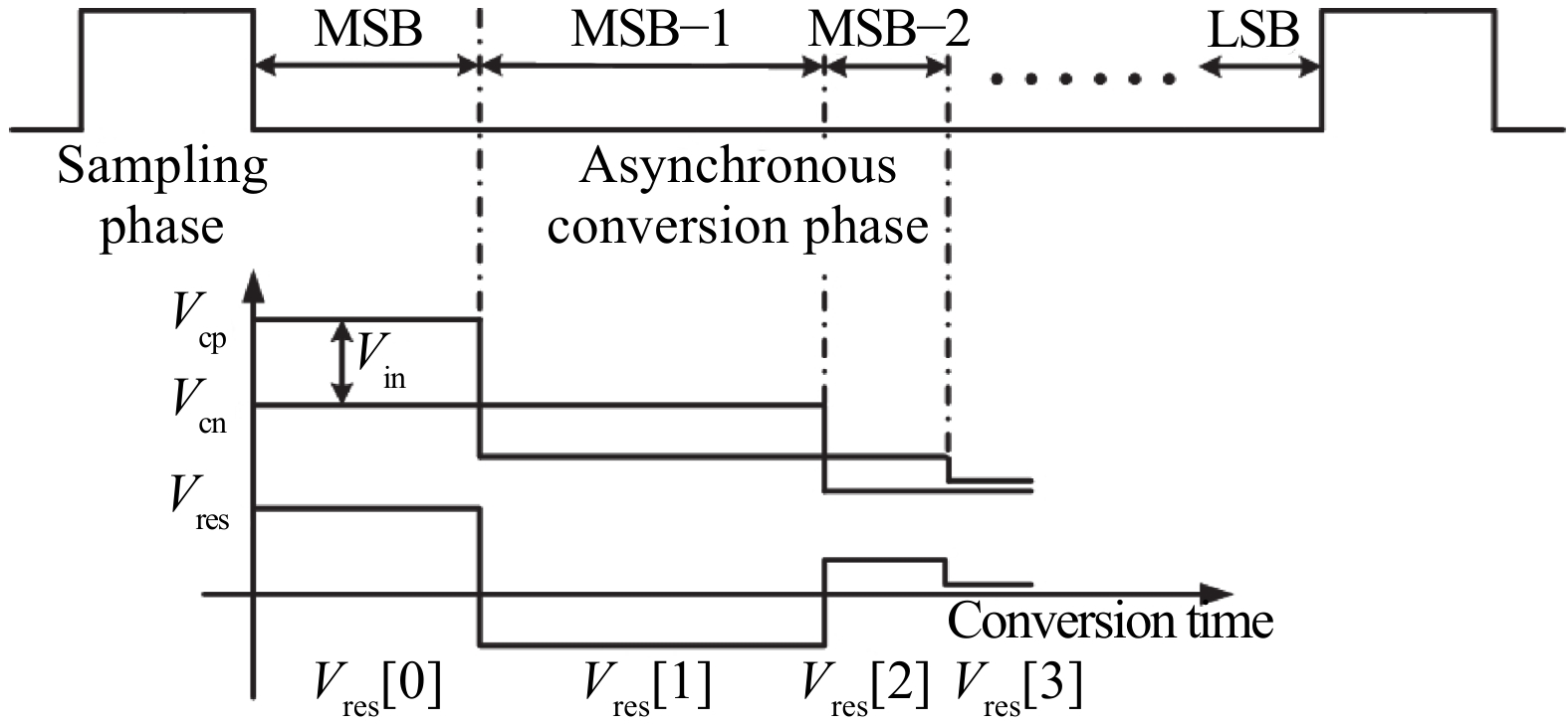
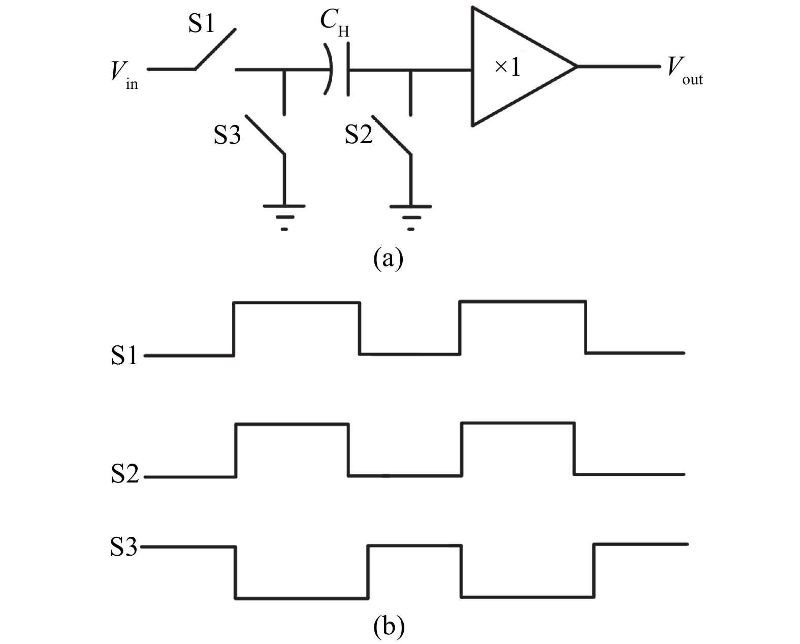
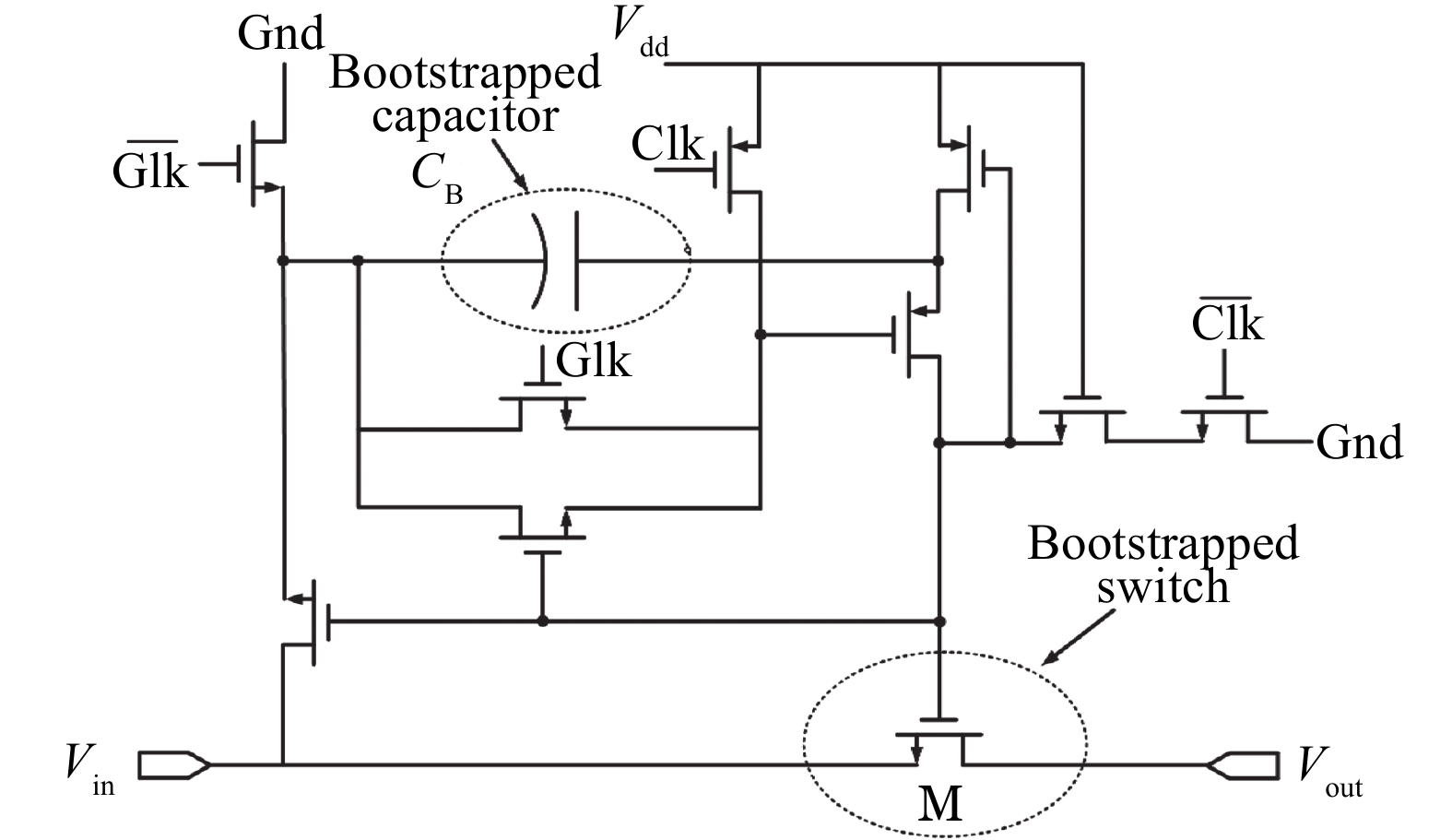
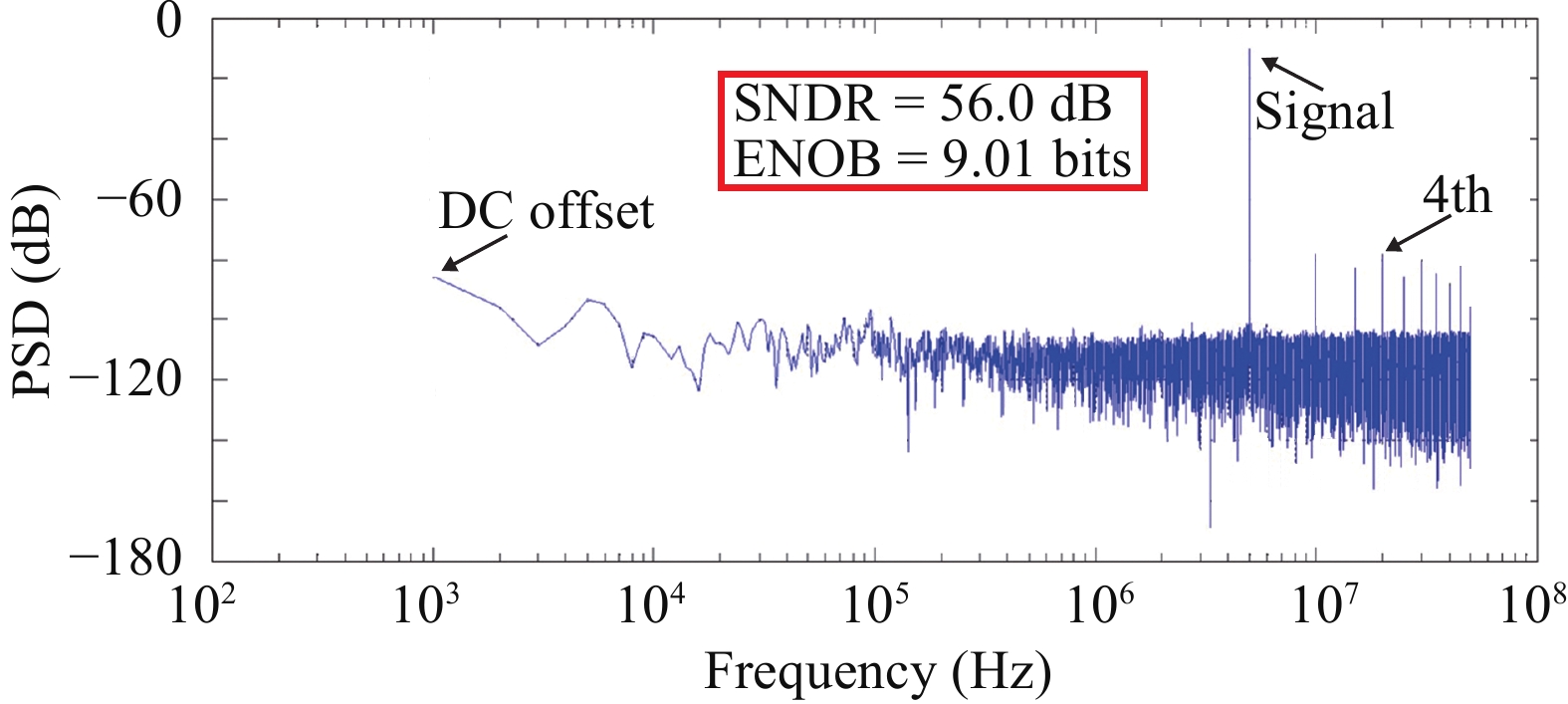
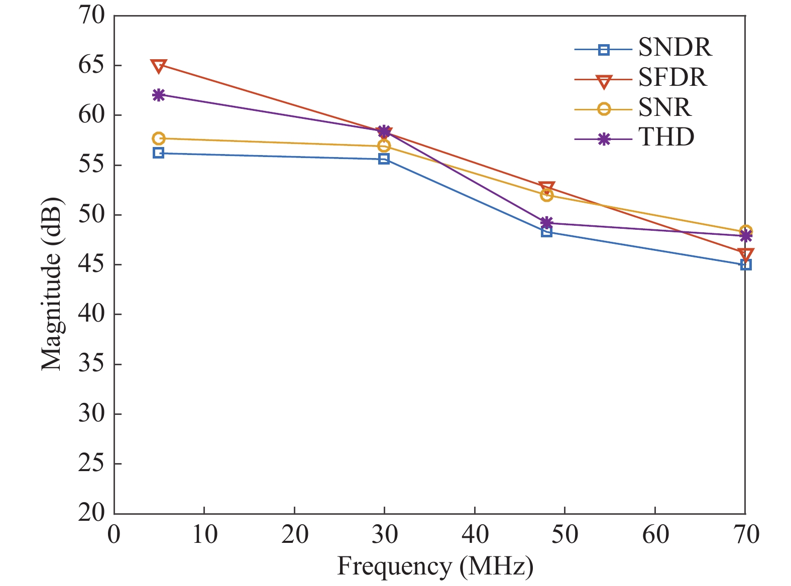
This paper presents a power-efficient 100-MS/s, 10-bit asynchronous successive approximation register (SAR) ADC. It includes an on-chip reference buffer and the total power dissipation is 6.8 mW. To achieve high performance with high power-efficiency in the proposed ADC, bootstrapped switch, redundancy, set-and-down switching approach, dynamic comparator and dynamic logic techniques are employed. The prototype was fabricated using 65 nm standard CMOS technology. At a 1.2-V supply and 100 MS/s, the ADC achieves an SNDR of 56.2 dB and a SFDR of 65.1 dB. The ADC core consumes only 3.1 mW, resulting in a figure of merit (FOM) of 30.27 fJ/conversionstep and occupies an active area of only 0.009 mm2.

J. Semicond.
2017, 38(10): 105002 doi: 10.1088/1674-4926/38/10/105002
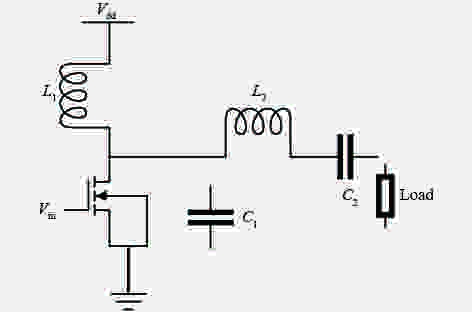
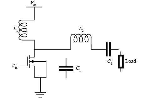
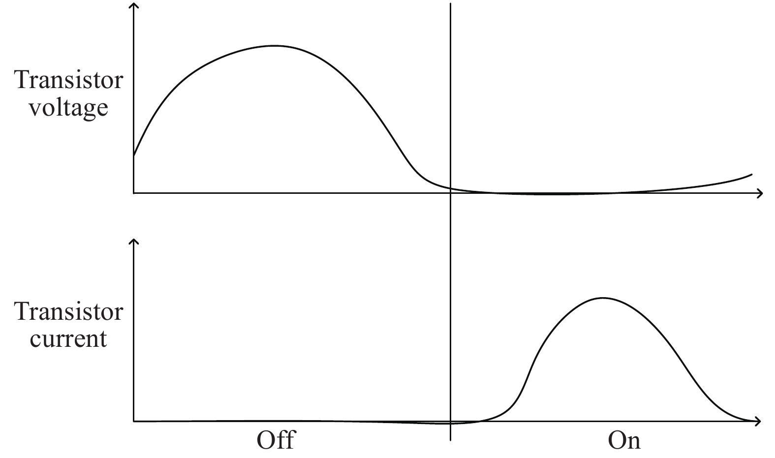
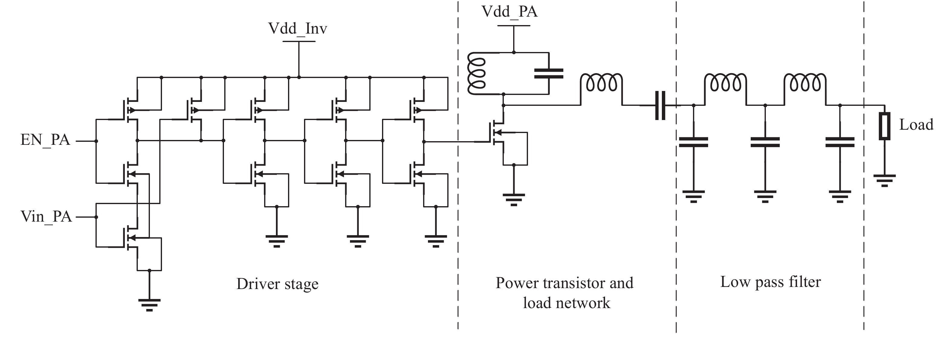
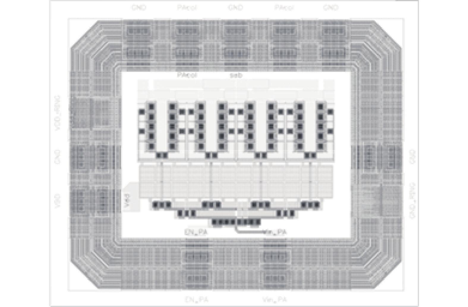
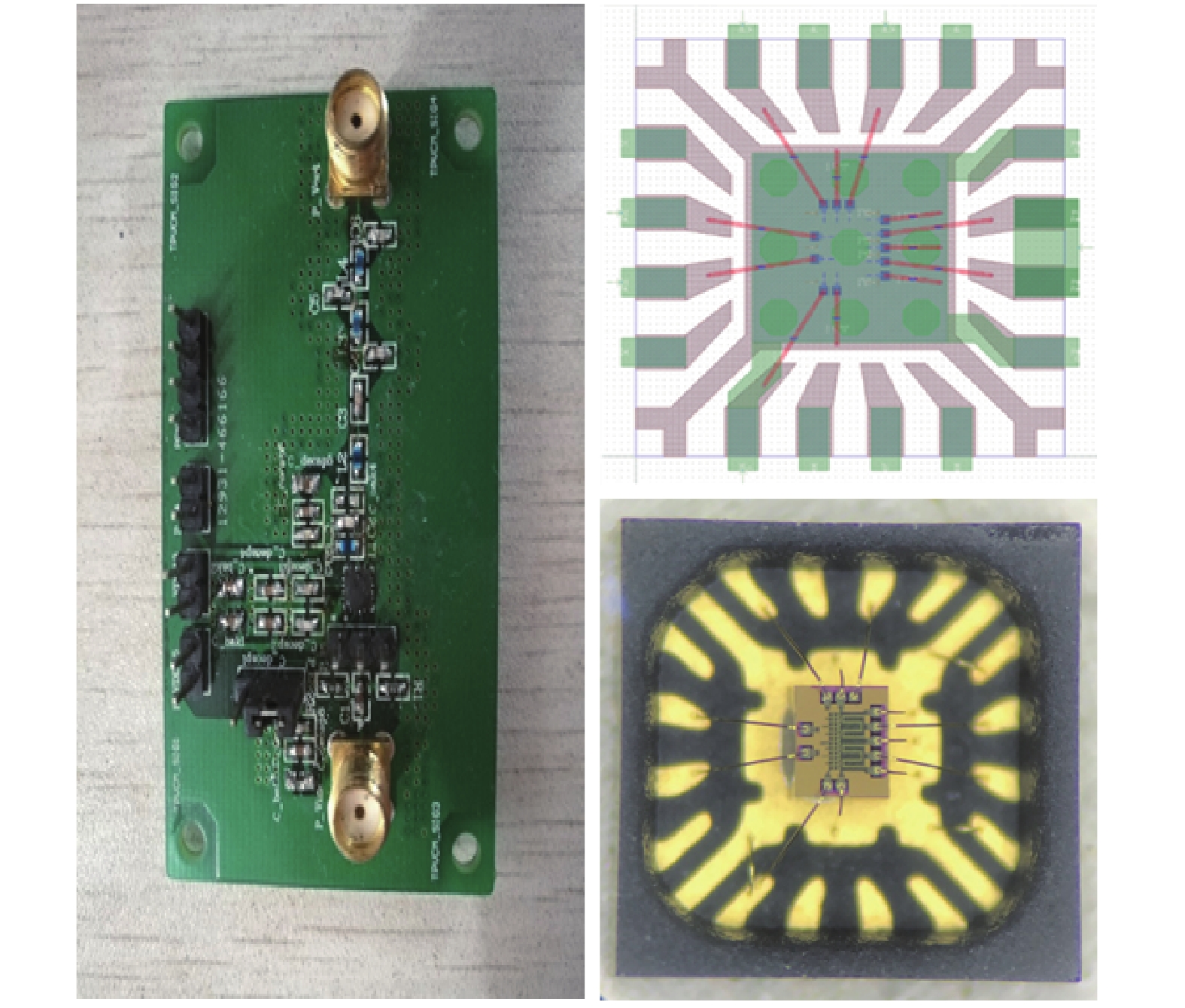
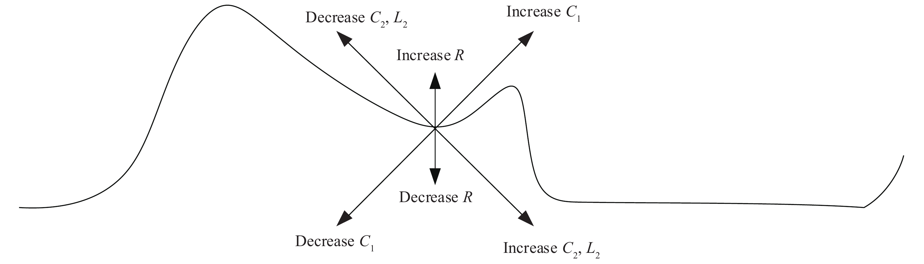
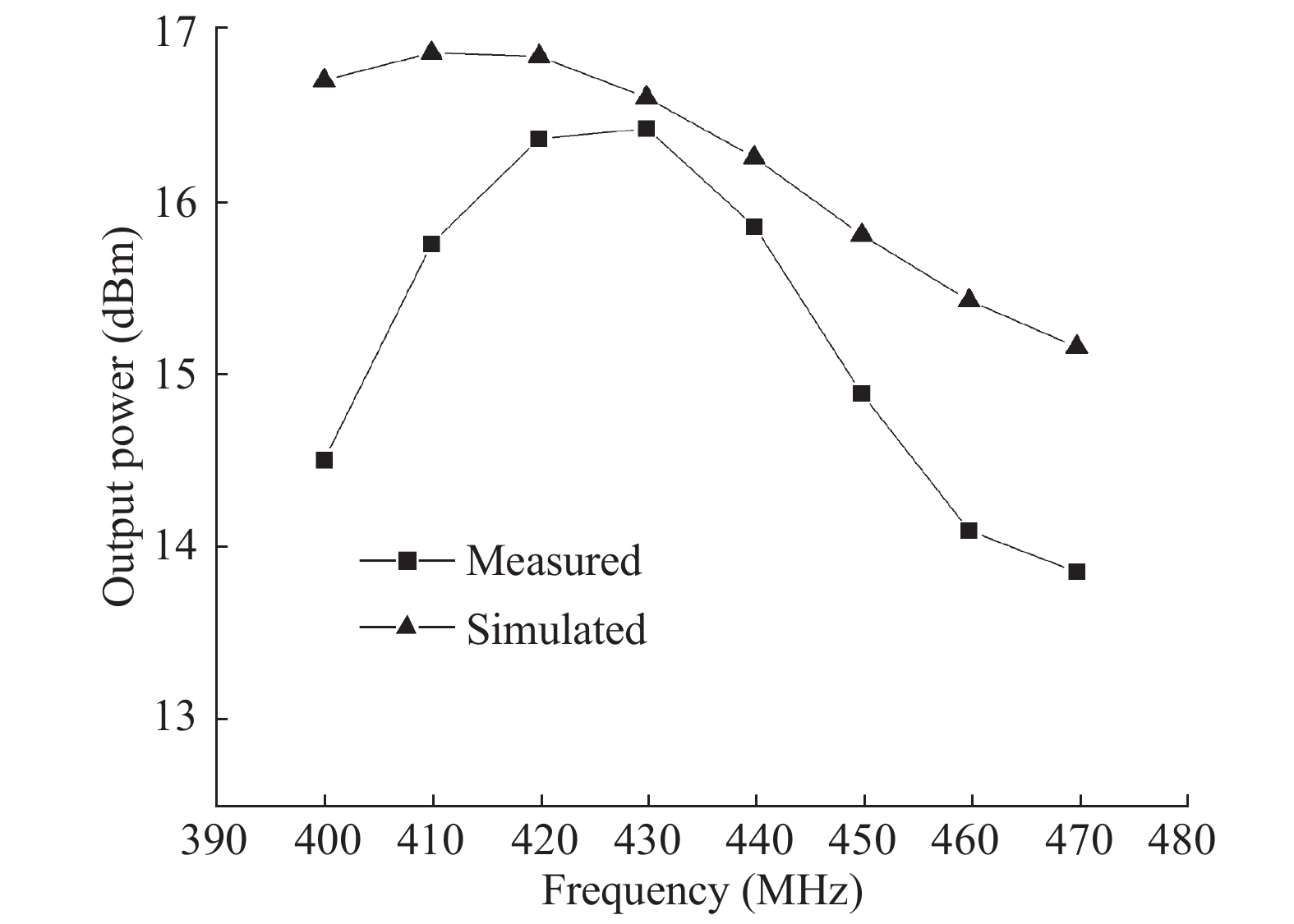
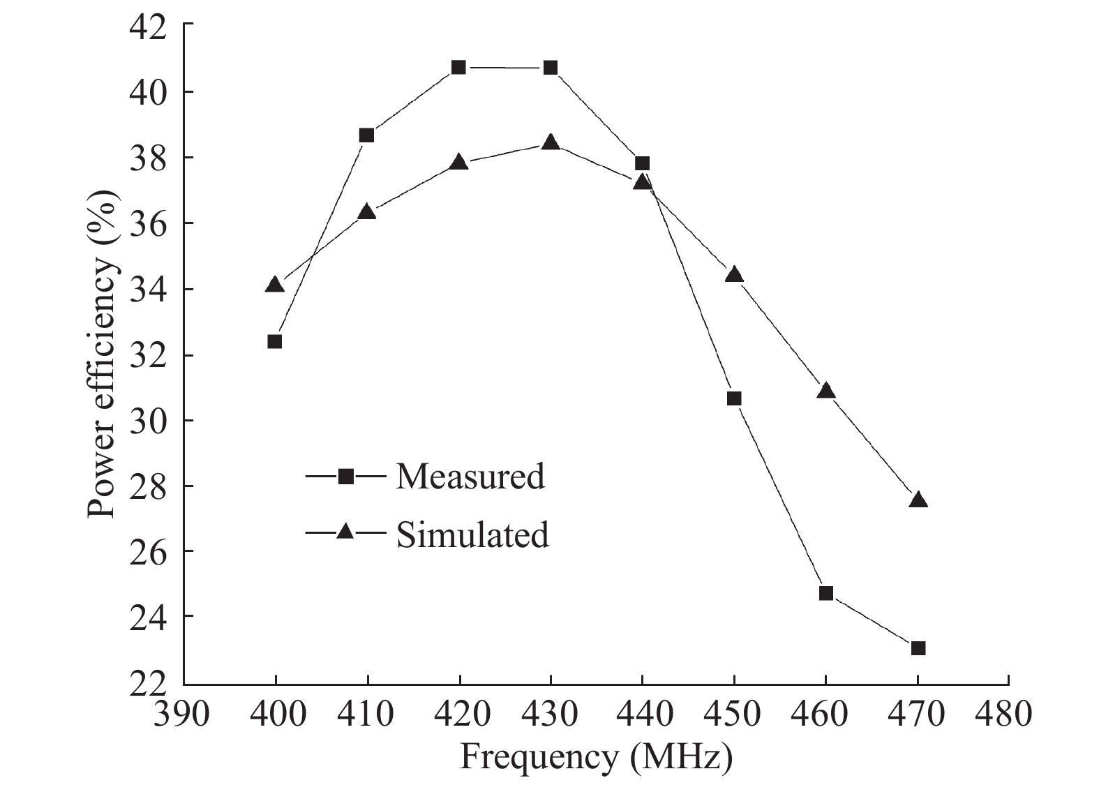
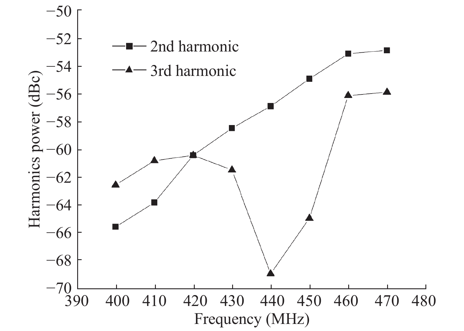
We present and propose a complete and iterative integrated-circuit and electro-magnetic (EM) co-design methodology and procedure for a low-voltage sub-1 GHz class-E PA. The presented class-E PA consists of the on-chip power transistor, the on-chip gate driving circuits, the off-chip tunable LC load network and the off-chip LC ladder low pass filter. The design methodology includes an explicit design equation based circuit components values' analysis and numerical derivation, output power targeted transistor size and low pass filter design, and power efficiency oriented design optimization. The proposed design procedure includes the power efficiency oriented LC network tuning, the detailed circuit/EM co-simulation plan on integrated circuit level, package level and PCB level to ensure an accurate simulation to measurement match and first pass design success. The proposed PA is targeted to achieve more than 15 dBm output power delivery and 40% power efficiency at 433 MHz frequency band with 1.5 V low voltage supply. The LC load network is designed to be off-chip for the purpose of easy tuning and optimization. The same circuit can be extended to all sub-1 GHz applications with the same tuning and optimization on the load network at different frequencies. The amplifier is implemented in 0.13 μm CMOS technology with a core area occupation of 400 μm by 300 μm. Measurement results showed that it provided power delivery of 16.42 dBm at antenna with efficiency of 40.6%. A harmonics suppression of 44 dBc is achieved, making it suitable for massive deployment of IoT devices.
J. Semicond.
2017, 38(10): 105003 doi: 10.1088/1674-4926/38/10/105003

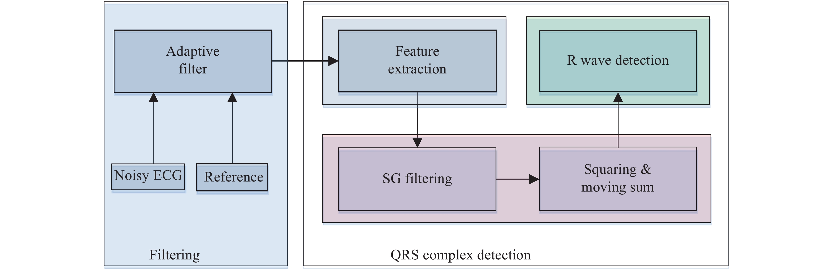
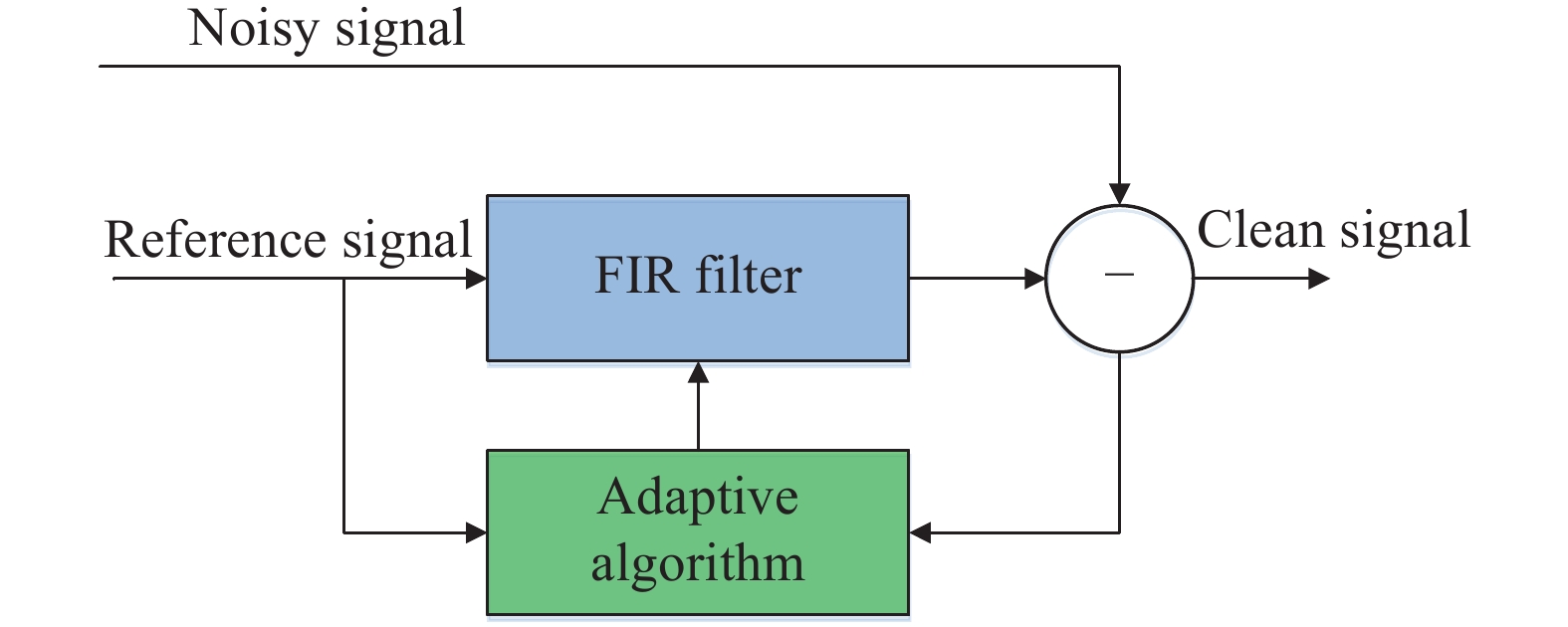
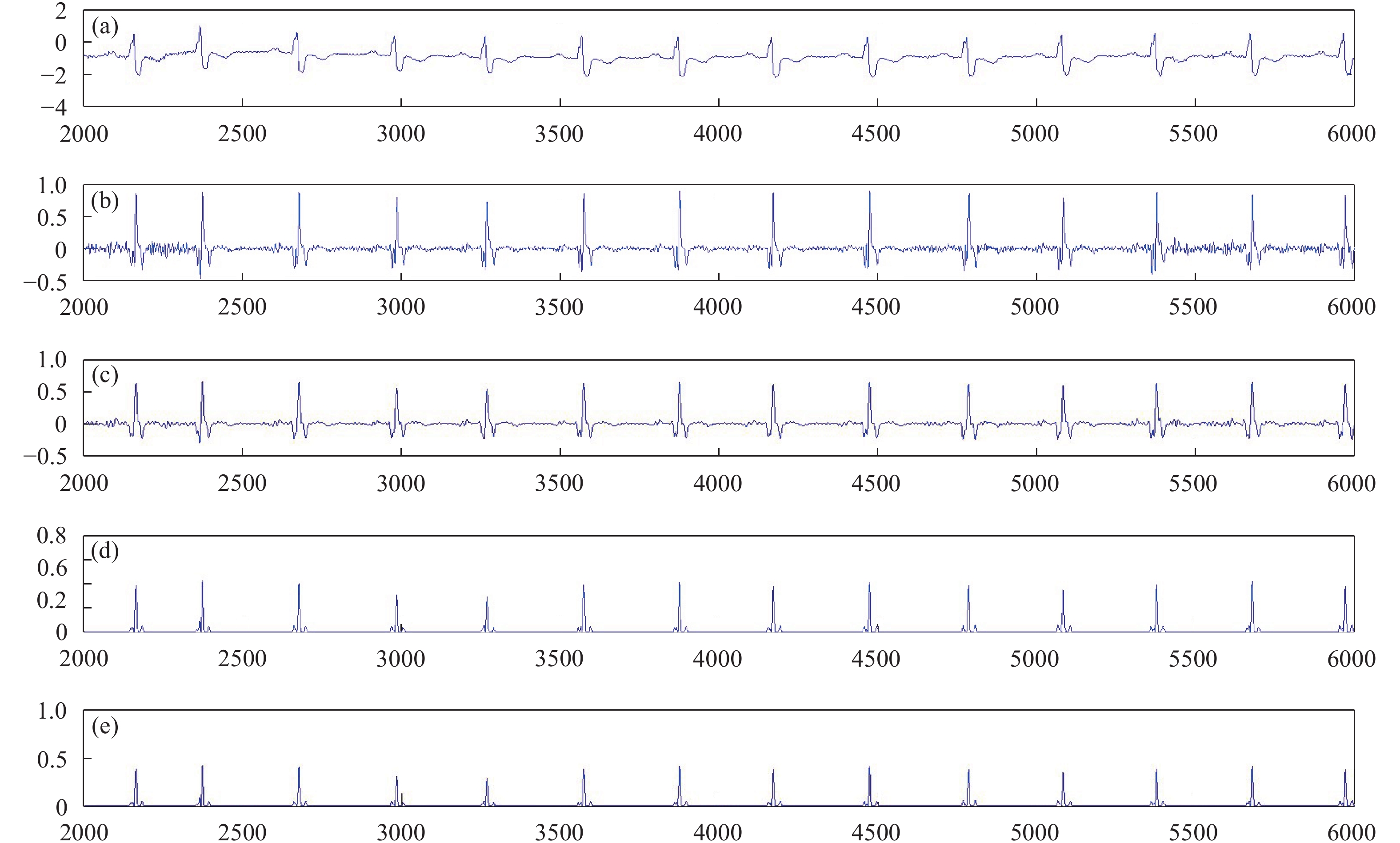
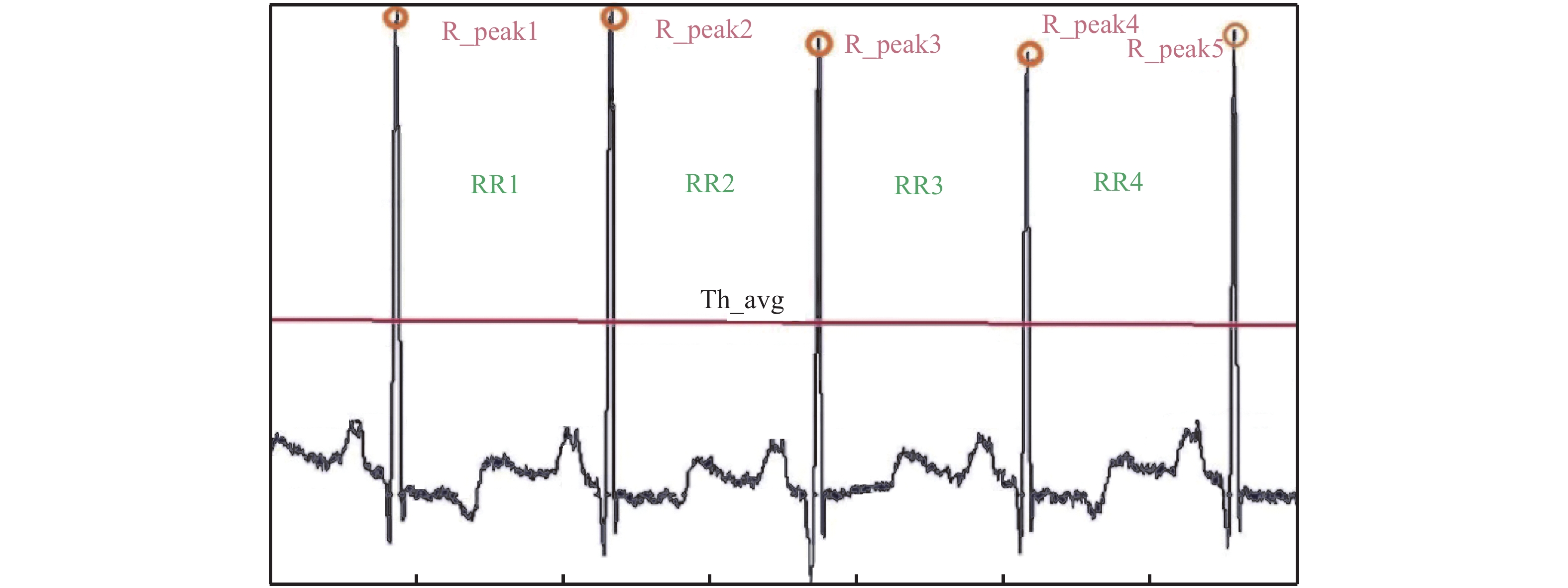
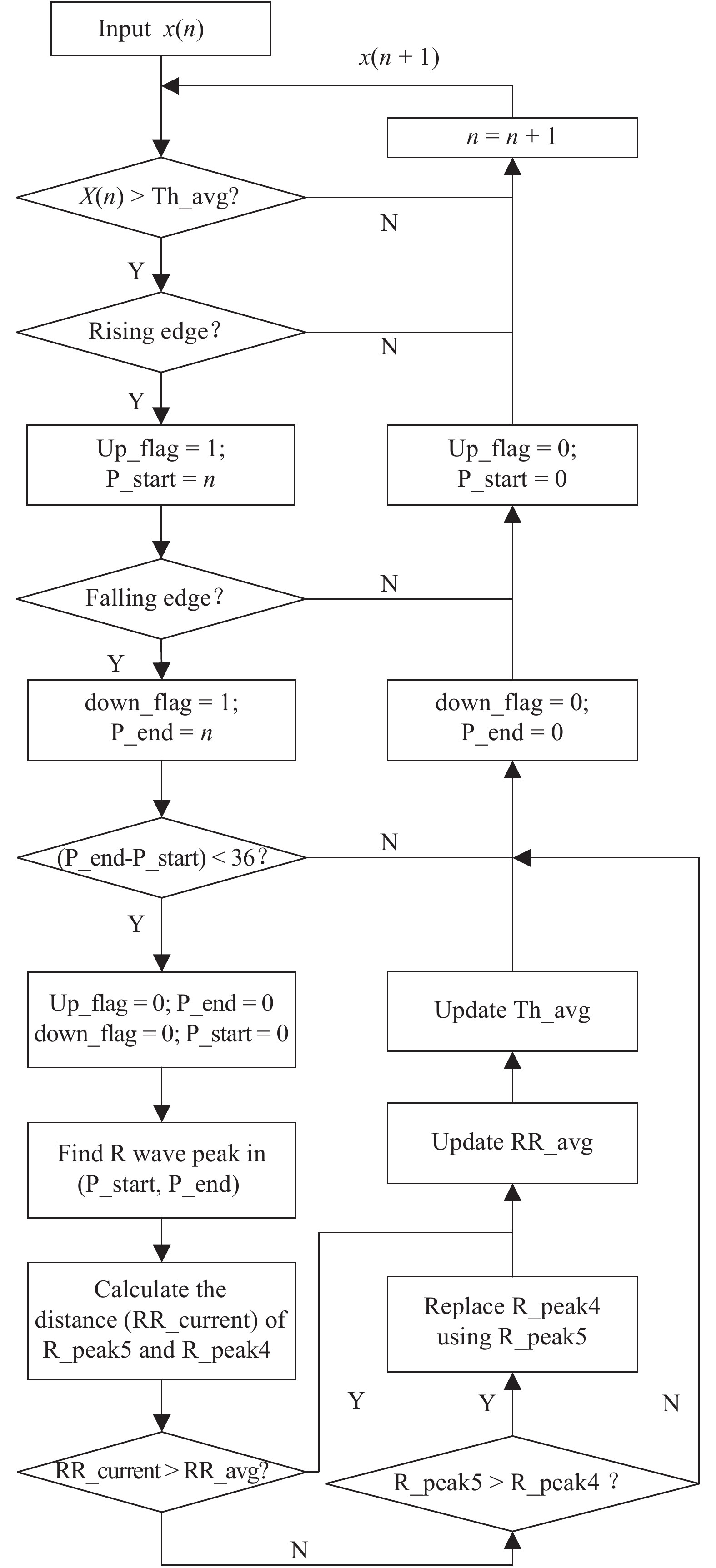
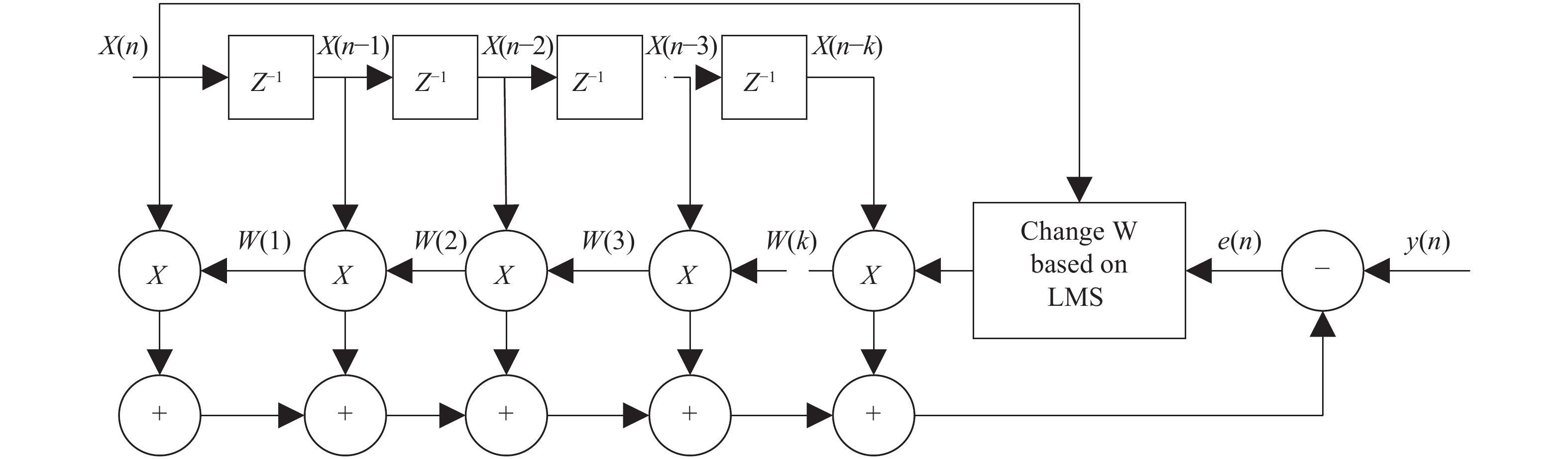
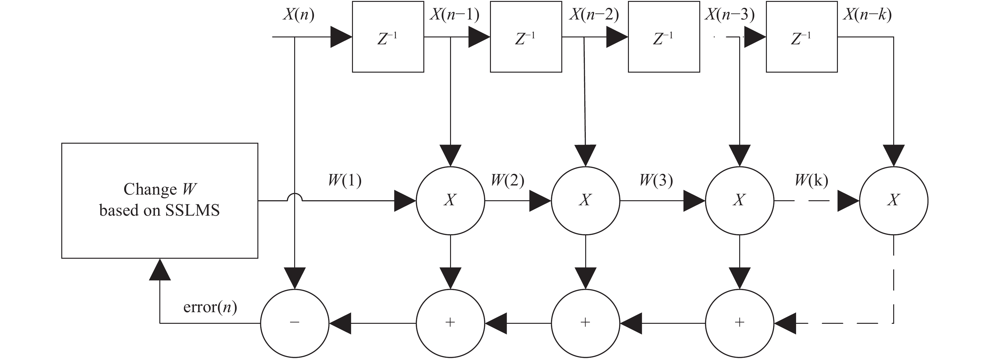
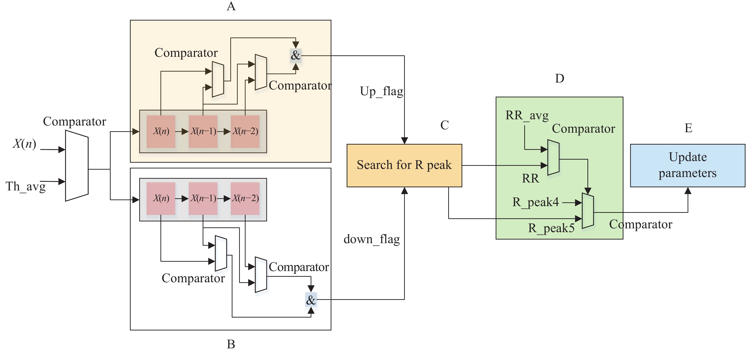
Electrocardiogram (ECG) can be used as a valid way for diagnosing heart disease. To fulfill ECG processing in wearable devices by reducing computation complexity and hardware cost, two kinds of adaptive filters are designed to perform QRS complex detection and motion artifacts removal, respectively. The proposed design achieves a sensitivity of 99.49% and a positive predictivity of 99.72%, tested under the MIT-BIH ECG database. The proposed design is synthesized under the SMIC 65-nm CMOS technology and verified by post-synthesis simulation. Experimental results show that the power consumption and area cost of this design are of 160 μW and 1.09 × 10 5 μm2, respectively.

J. Semicond.
2017, 38(10): 105004 doi: 10.1088/1674-4926/38/10/105004
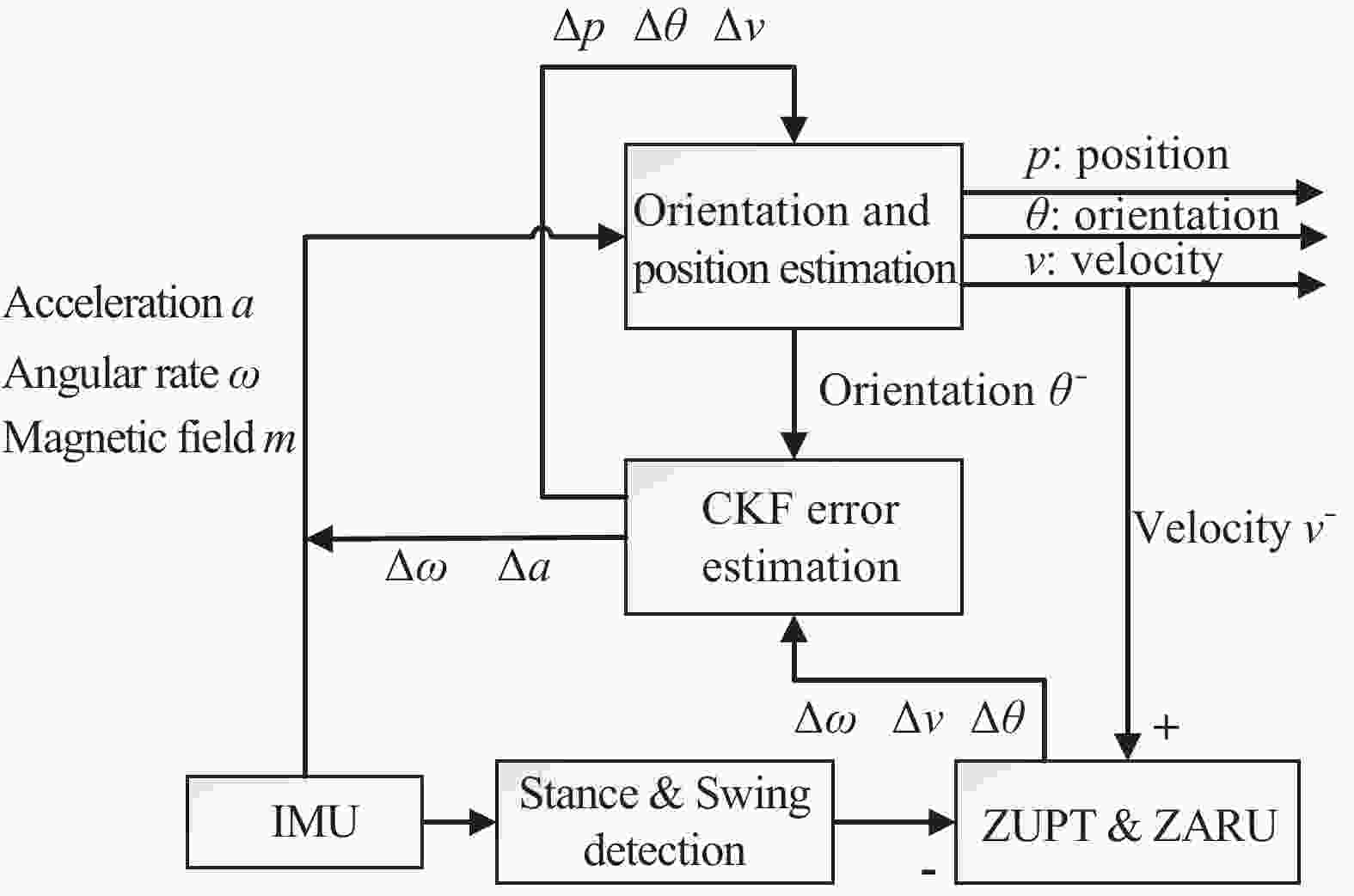
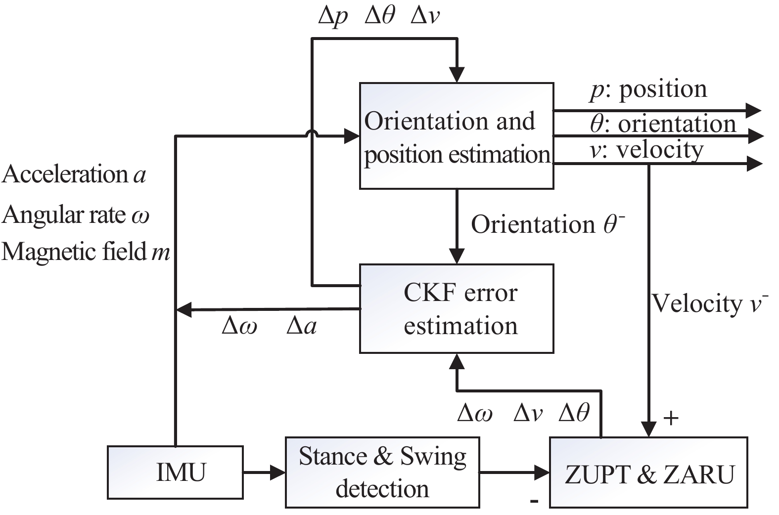
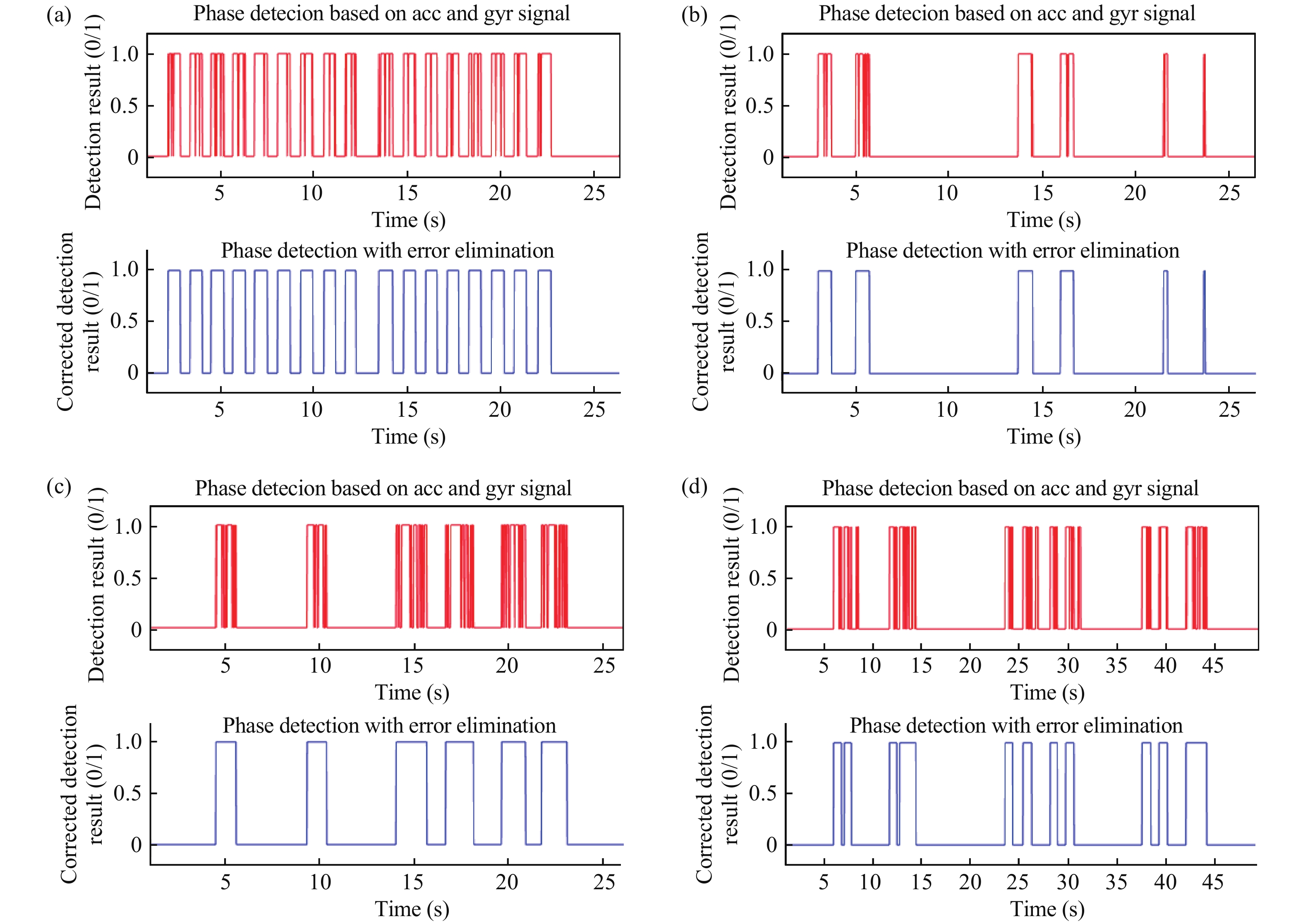
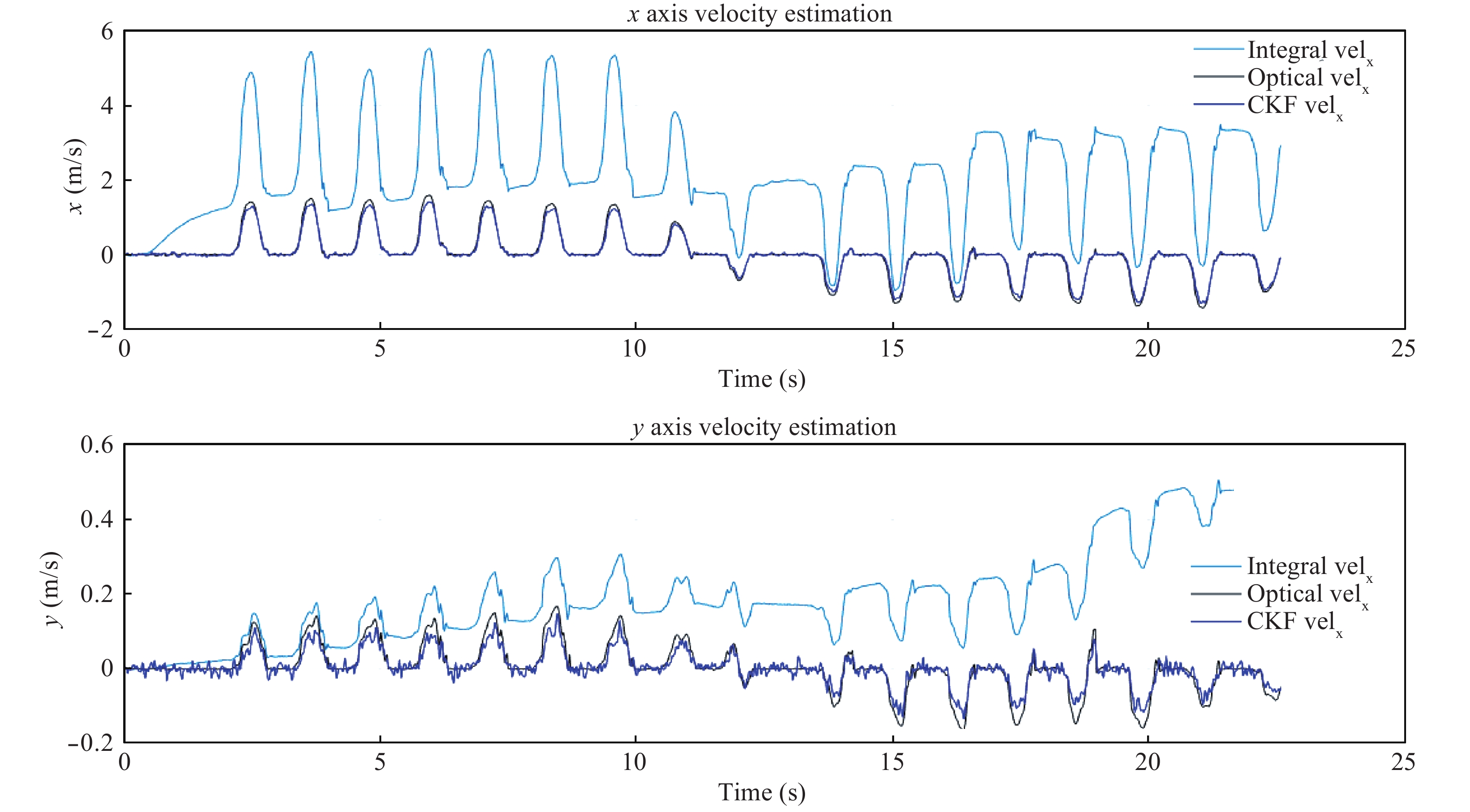
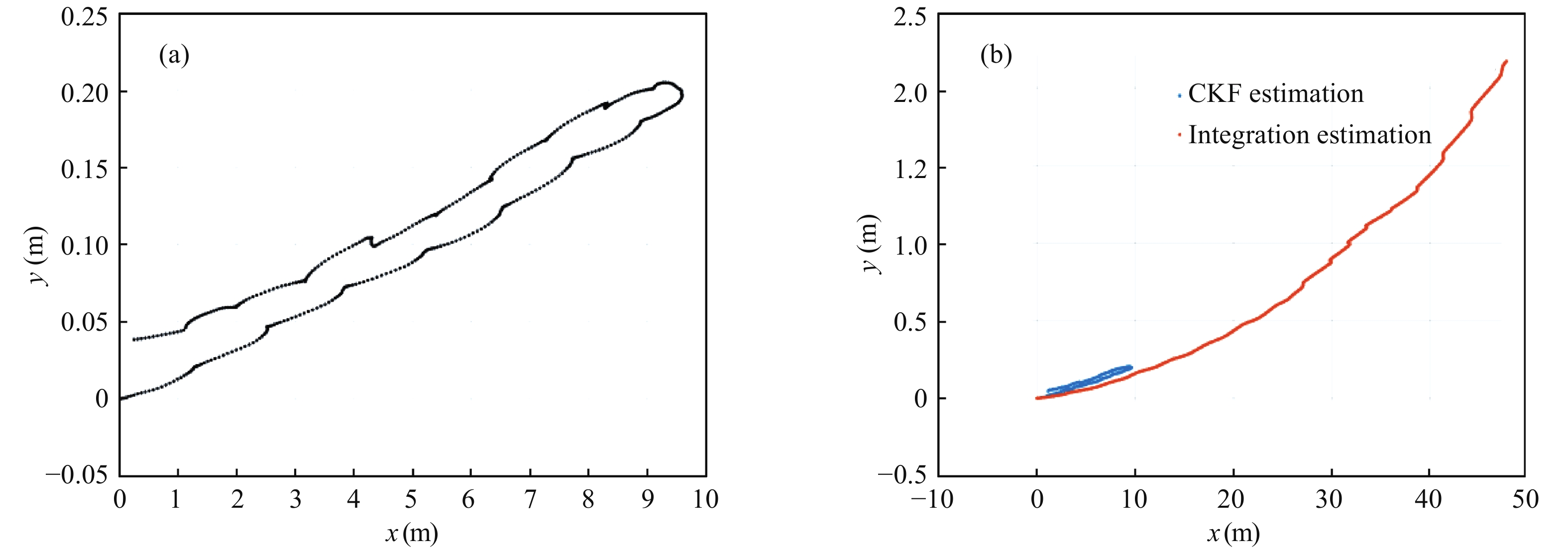
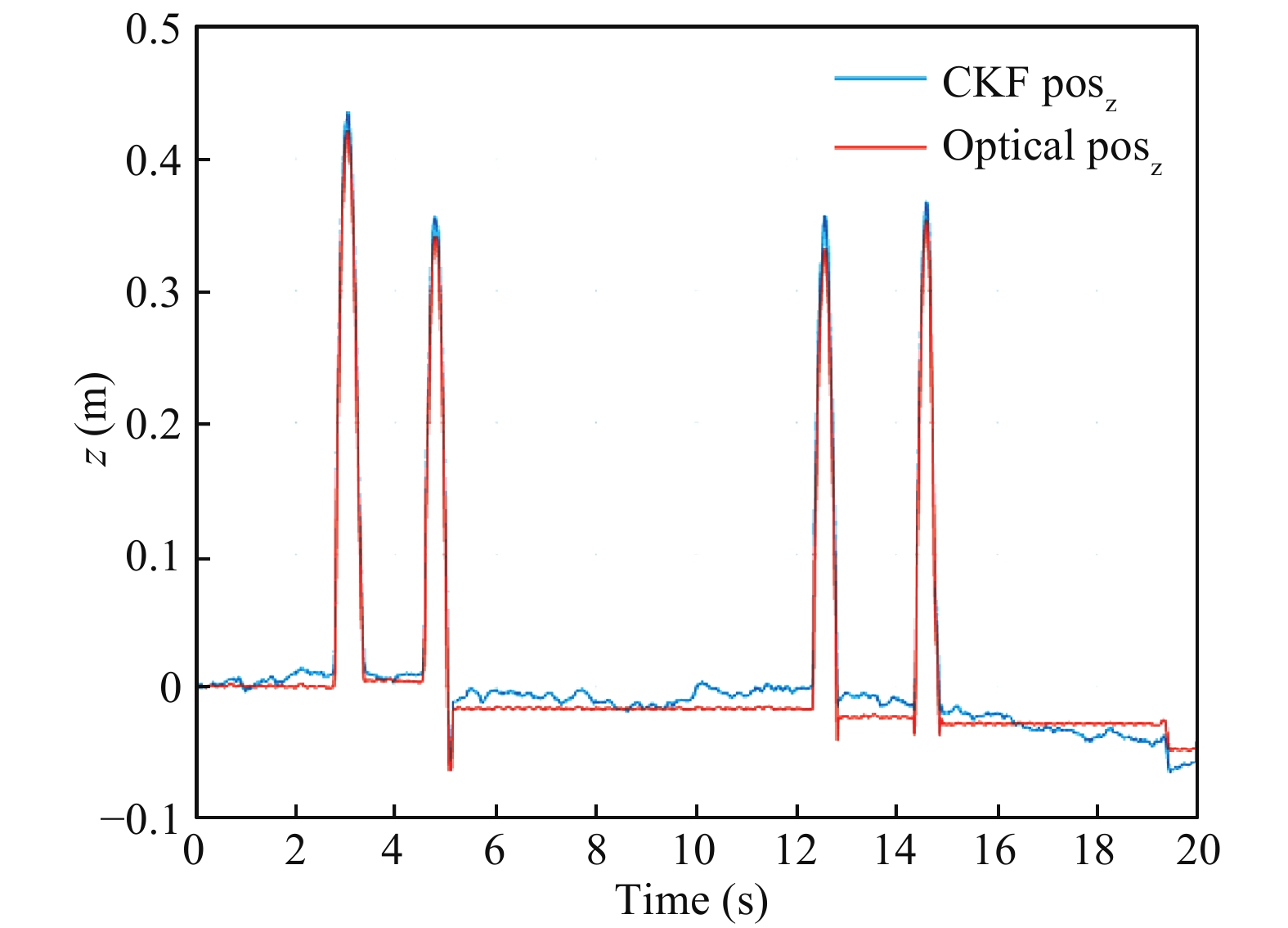
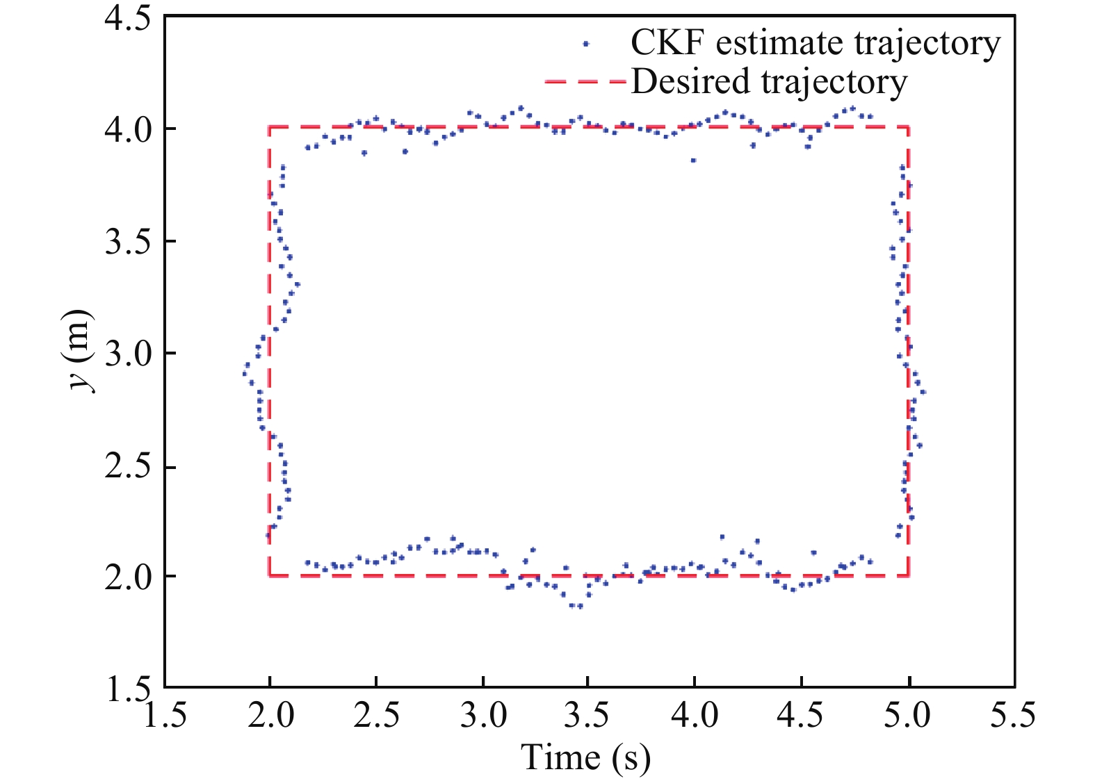
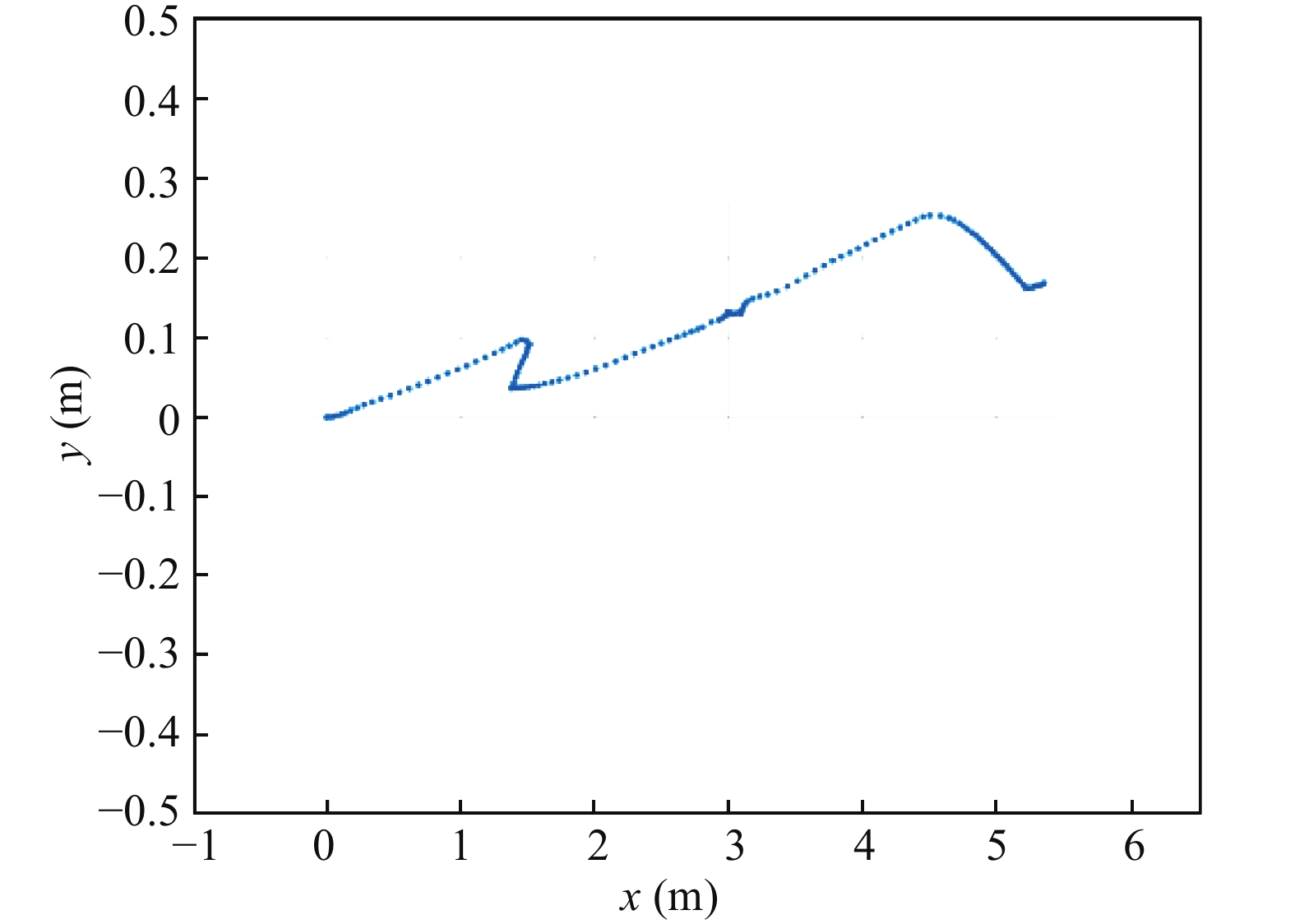
A wearable micro-sensor motion capture system with 16 IMUs and an error-compensatory complementary filter algorithm for real-time motion estimation has been developed to acquire accurate 3D orientation and displacement in real life activities. In the proposed filter algorithm, the gyroscope bias error, orientation error and magnetic disturbance error are estimated and compensated, significantly reducing the orientation estimation error due to sensor noise and drift. Displacement estimation, especially for activities such as jumping, has been the challenge in micro-sensor motion capture. An adaptive gait phase detection algorithm has been developed to accommodate accurate displacement estimation in different types of activities. The performance of this system is benchmarked with respect to the results of VICON optical capture system. The experimental results have demonstrated effectiveness of the system in daily activities tracking, with estimation error 0.16 ± 0.06 m for normal walking and 0.13 ± 0.11 m for jumping motions.


J. Semicond.
2017, 38(10): 105005 doi: 10.1088/1674-4926/38/10/105005
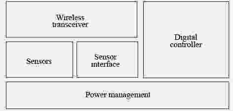
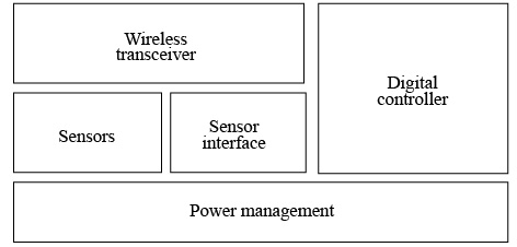
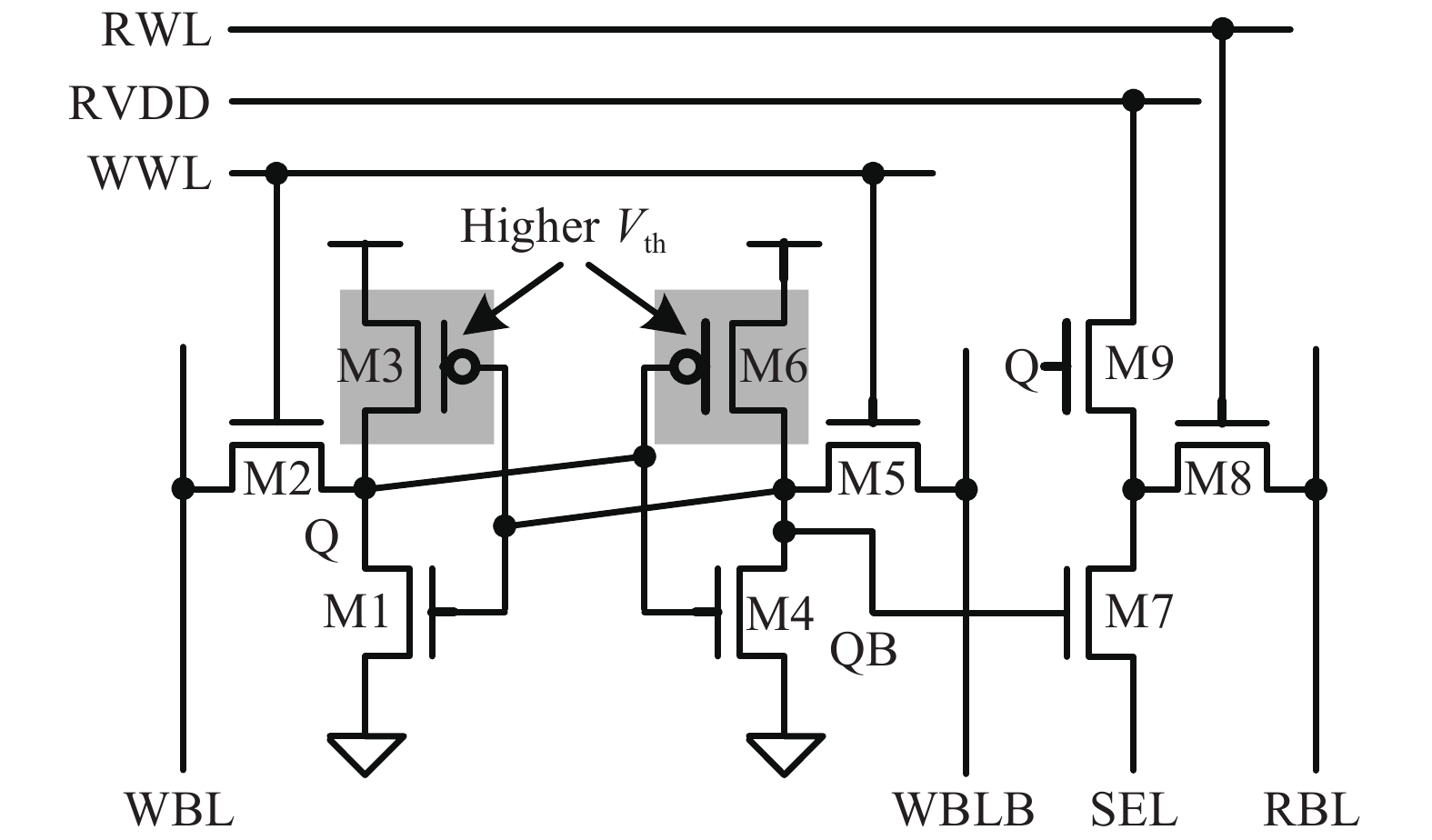
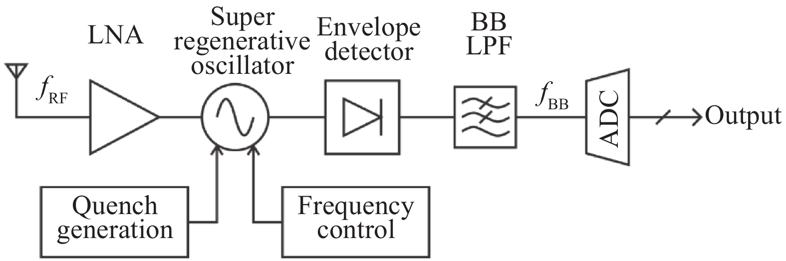
Wireless smart sensing is now widely used in various applications such as health monitoring and structural monitoring. In conventional wireless sensor nodes, significant power is consumed in wirelessly transmitting the raw data. Smart sensing adds local intelligence to the sensor node and reduces the amount of wireless data transmission via on-node digital signal processing. While the total power consumption is reduced compared to conventional wireless sensing, the power consumption of the digital processing becomes as dominant as wireless data transmission. This paper reviews the state-of-the-art energy-efficient digital and wireless IC design techniques for reducing the power consumption of the wireless smart sensor node to prolong battery life and enable self-powered applications.


J. Semicond.
2017, 38(10): 103001 doi: 10.1088/1674-4926/38/10/103001

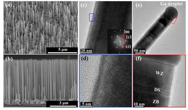
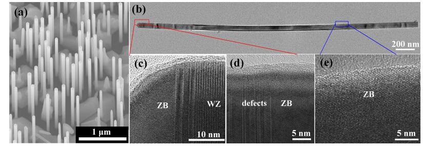
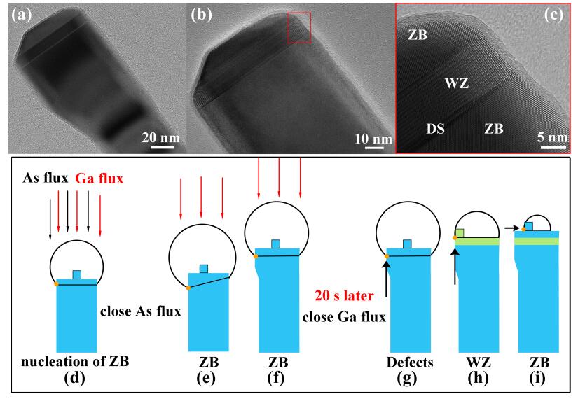
Self-catalyzed GaAs nanowires (NWs) are grown on Si (111) substrates by molecular-beam epitaxy. The effect of different closing sequences of the Ga and As cell shutters on the morphology and structural phase of GaAs NWs is investigated. For the sequences of closing the Ga and As cell shutters simultaneously or closing the As cell shutter 1 min after closing the Ga cell shutter, the NWs grow vertically to the substrate surface. In contrast, when the As cell shutter is closed first, maintaining the Ga flux is found to be critical for the following growth of GaAs NWs, which can change the growth direction from[111] to 〈111〉. The evolution of the morphology and structural phase transition at the tips of these GaAs NWs confirm that the triple-phase-line shift mode is at work even for the growth with different cell shutter closing sequences. Our work will provide new insights for better understanding of the growth mechanism and realizing of the morphology and structure control of the GaAs NWs.


J. Semicond.
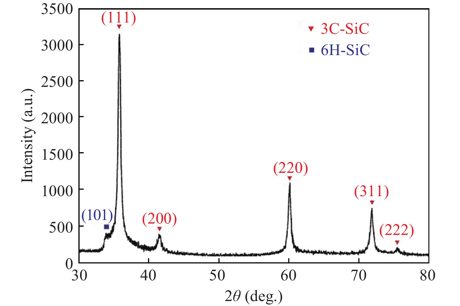
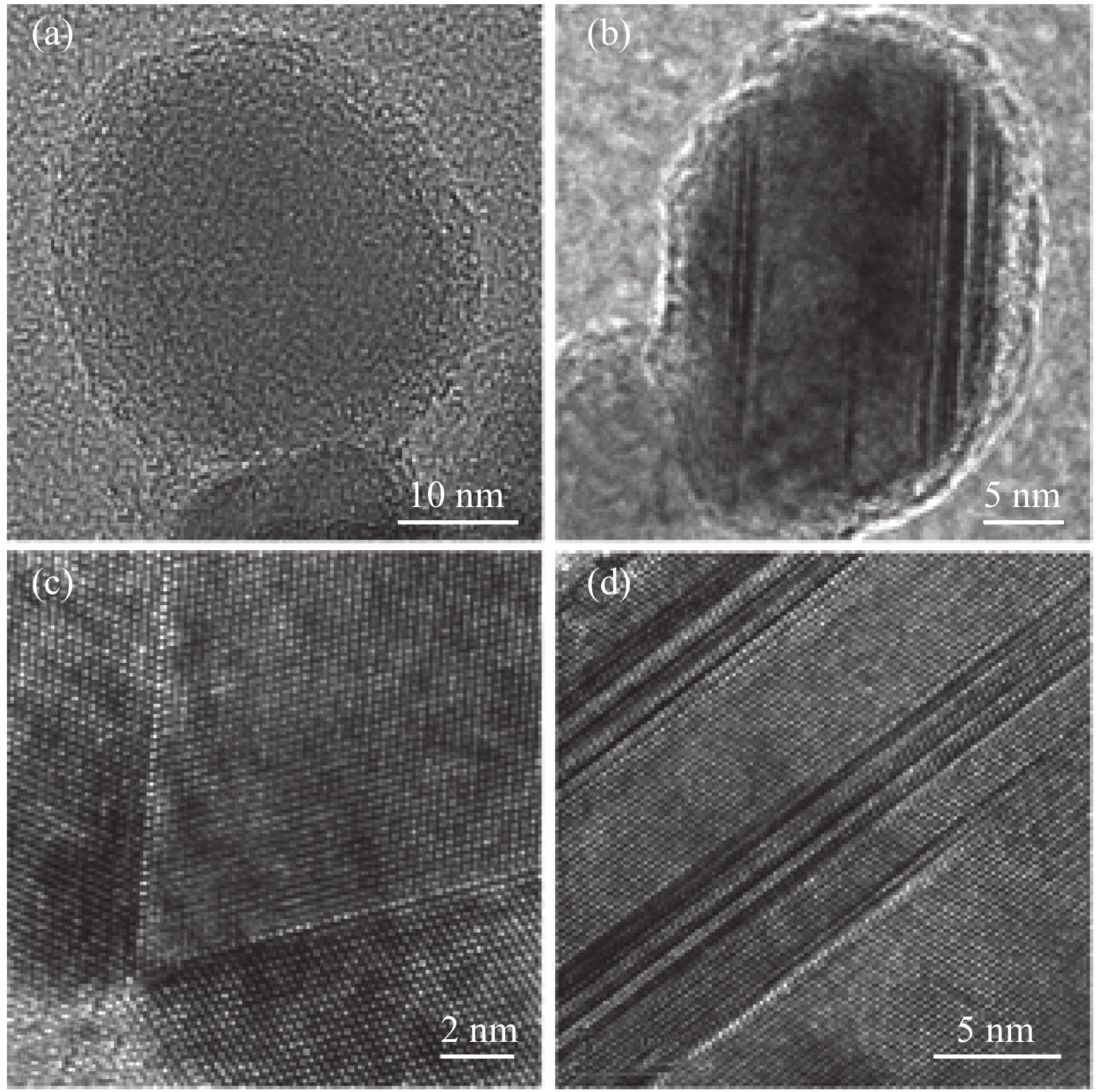
2017, 38(10): 103002 doi: 10.1088/1674-4926/38/10/103002

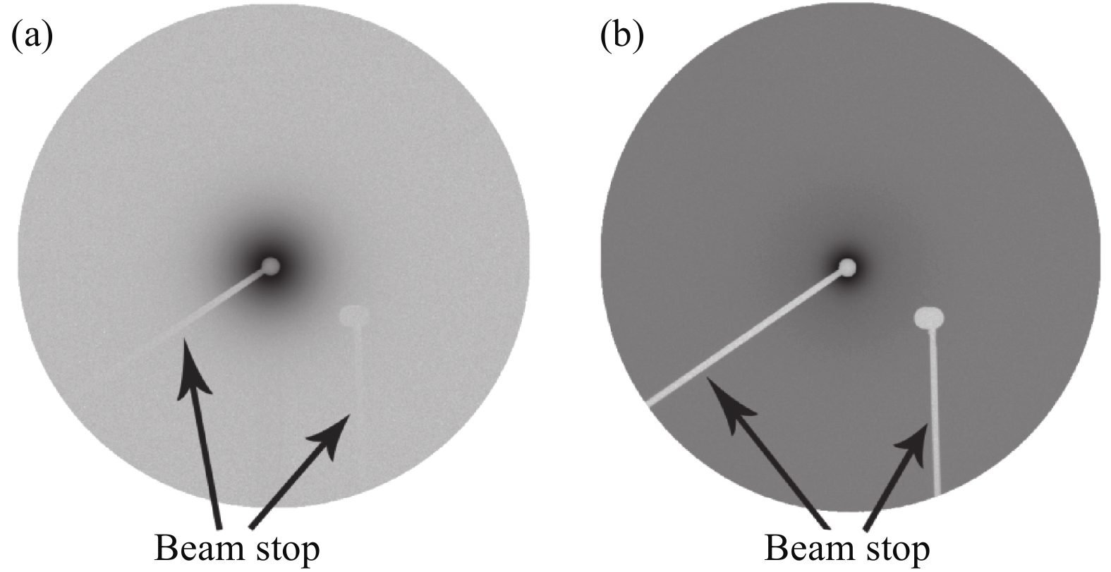
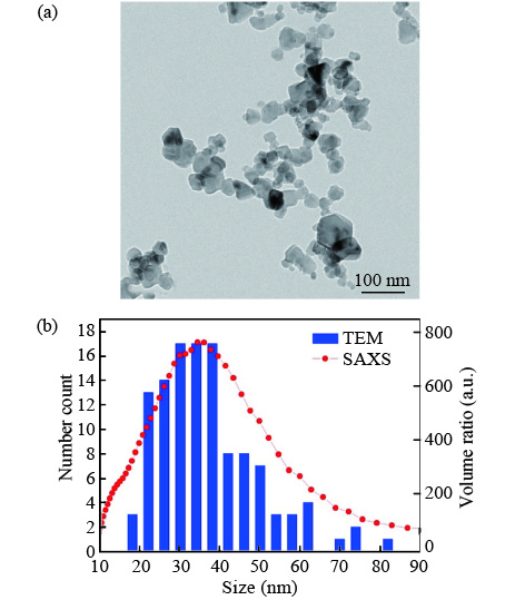
The structure and size of SiC nanoparticles were studied by different characterization methods including small angle X-ray scattering (SAXS), transmission electron microscope (TEM), and X-ray diffraction (XRD). The results showed that particle size distributions determined respectively from SAXS and TEM are comparable and follow the log-normal function. The size distribution of the particles is between 10 to 100 nm with most of them being in the range of 20–50 nm. The average particle size is around 42 nm. XRD identifies the phase of the SiC nanoparticles and suggests the average size of the single crystalline domain to be around 21 nm. The combined results from XRD and SAXS suggest the existence of many polycrystals, which is confirmed by the HRTEM observation of particles with twins and stacking faults. The material synthesis methods leading to various particle sizes are also discussed.

J. Semicond.
2017, 38(10): 104001 doi: 10.1088/1674-4926/38/10/104001
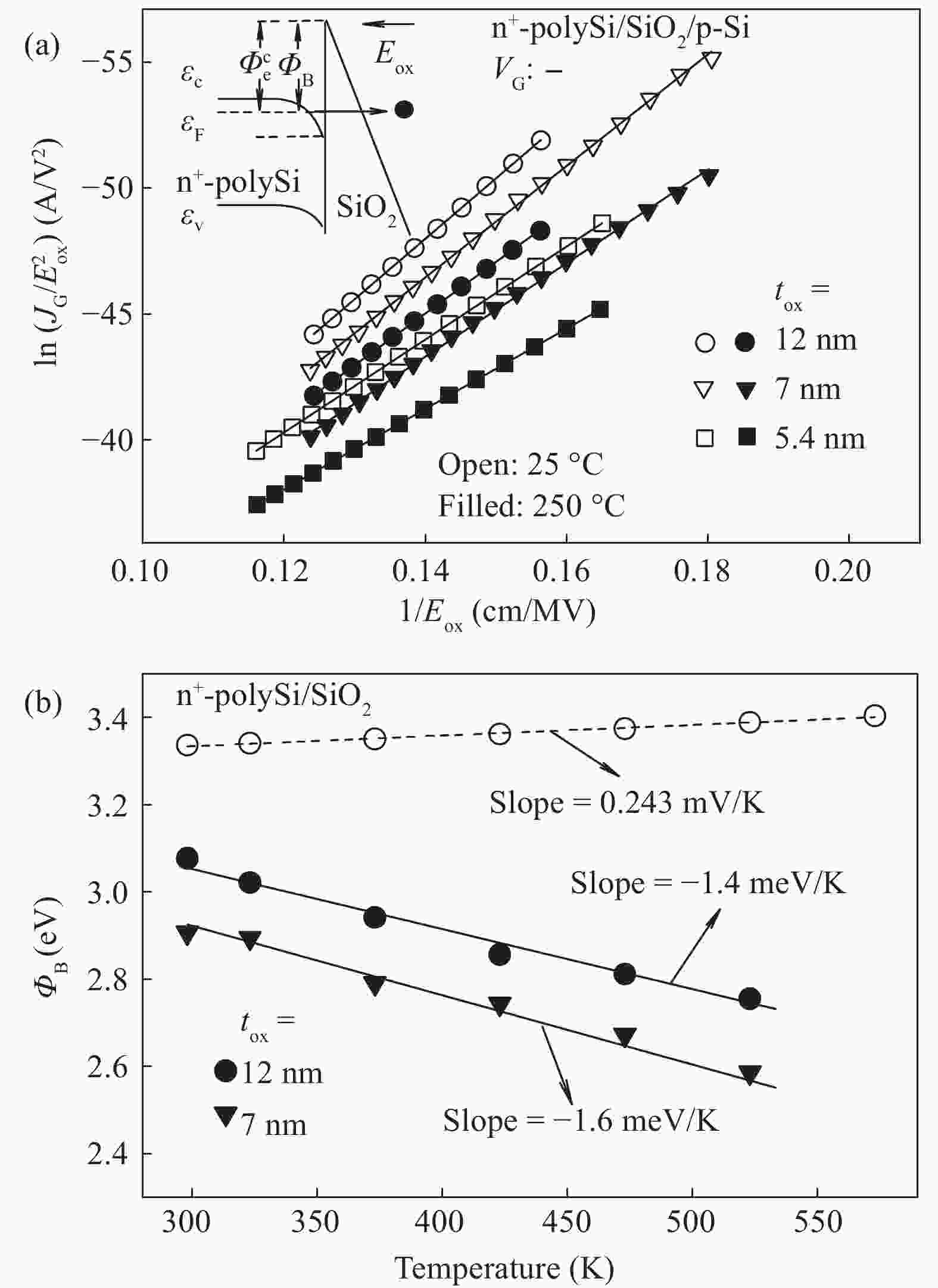
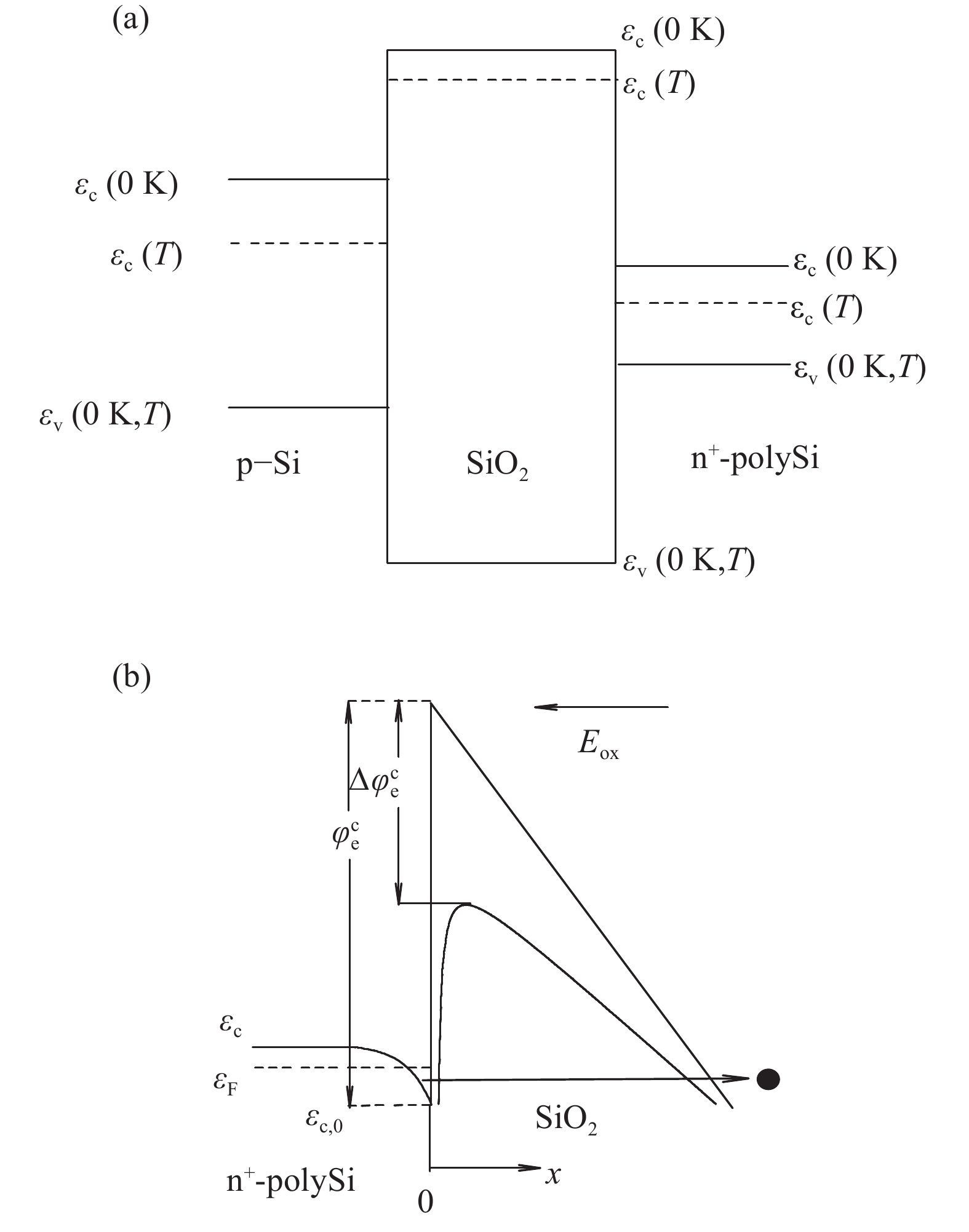
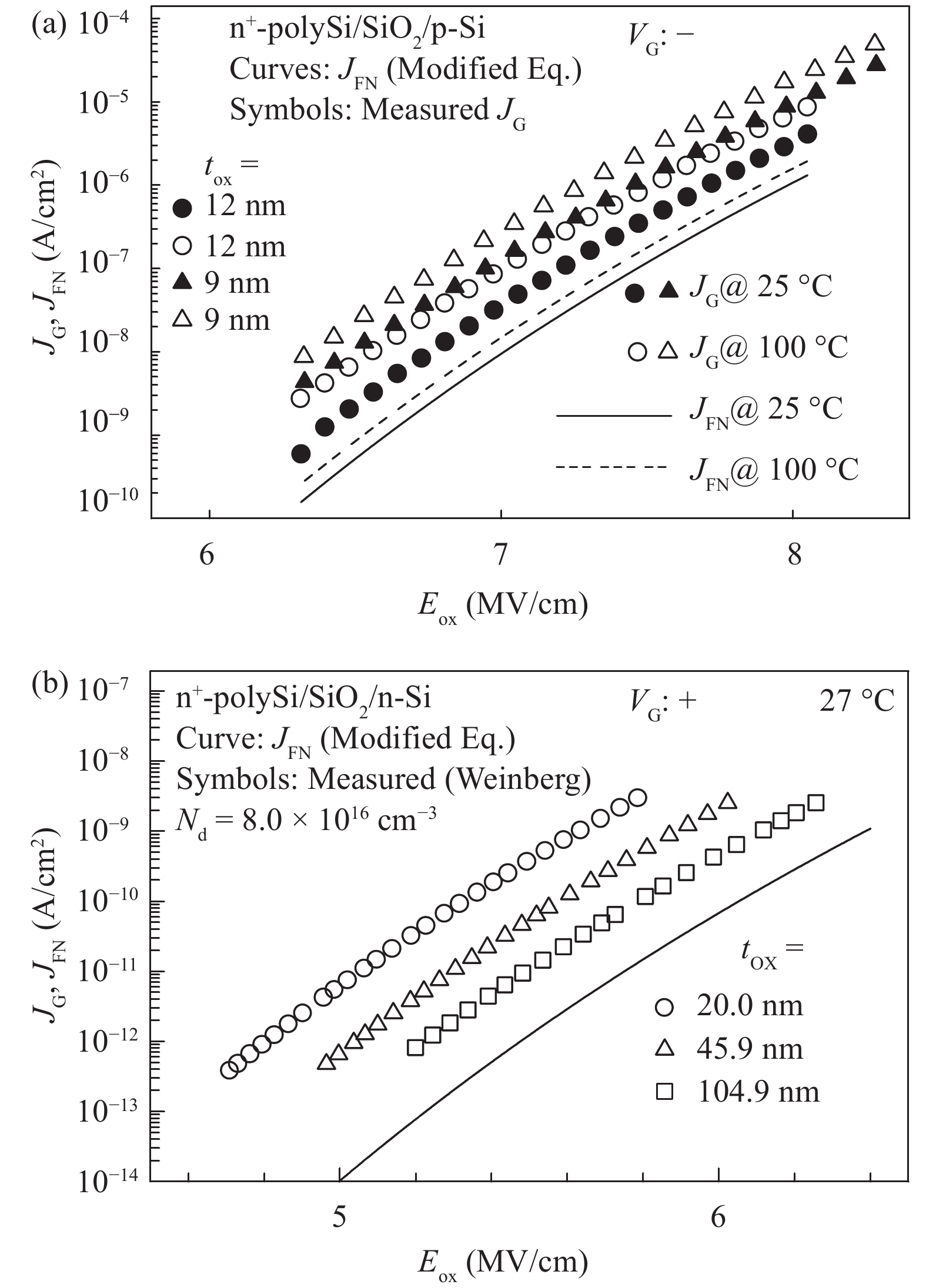
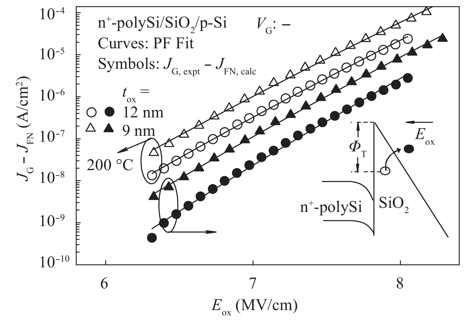
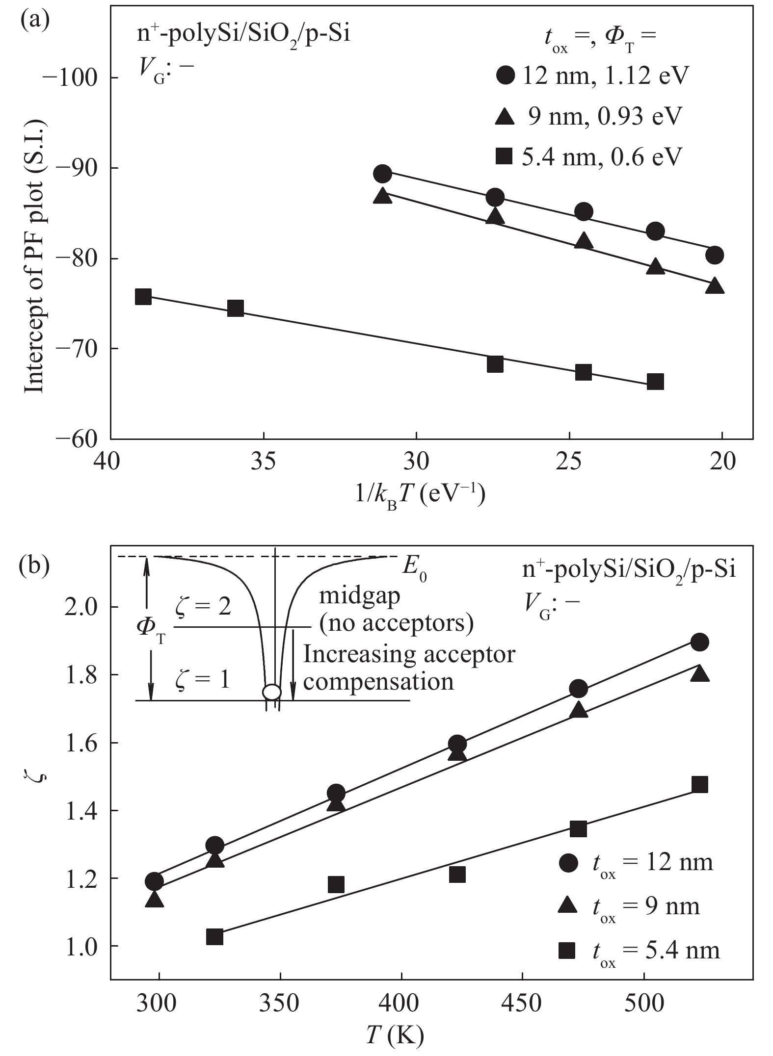
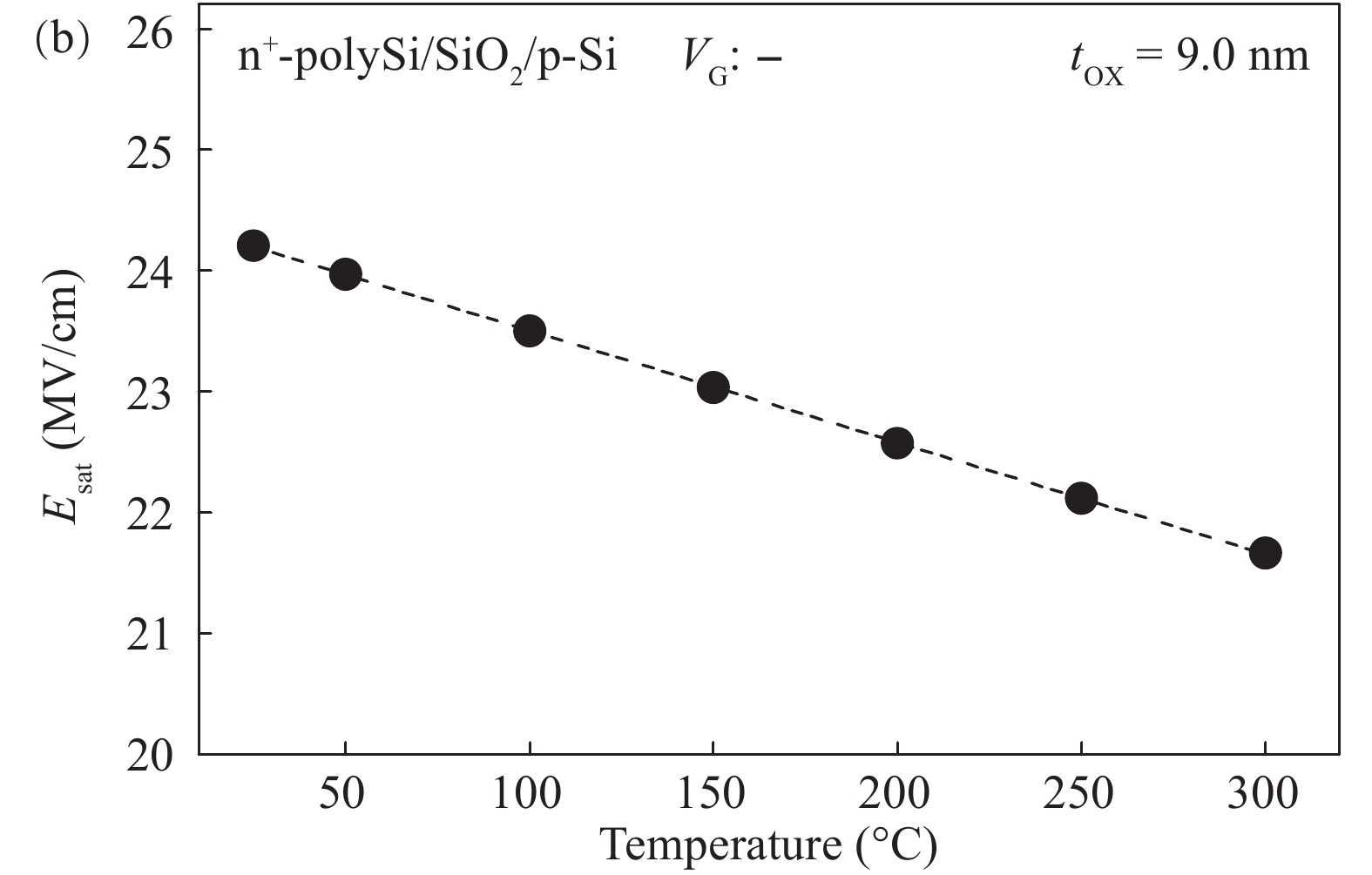
The conduction mechanism of gate leakage current through thermally grown silicon dioxide (SiO2) films on (100) p-type silicon has been investigated in detail under negative bias on the degenerately doped n-type polysilicon (n+-polySi) gate. The analysis utilizes the measured gate current density JG at high oxide fields Eox in 5.4 to 12 nm thick SiO2 films between 25 and 300 °C. The leakage current measured up to 300 °C was due to Fowler–Nordheim (FN) tunneling of electrons from the accumulated n +-polySi gate in conjunction with Poole Frenkel (PF) emission of trapped-electrons from the electron traps located at energy levels ranging from 0.6 to 1.12 eV (depending on the oxide thickness) below the SiO2 conduction band (CB). It was observed that PF emission current IPF dominates FN electron tunneling current IFN at oxide electric fields Eox between 6 and 10 MV/cm and throughout the temperature range studied here. Understanding of the mechanism of leakage current conduction through SiO2 films plays a crucial role in simulation of time-dependent dielectric breakdown (TDDB) of metaloxide–semiconductor (MOS) devices and to precisely predict the normal operating field or applied gate voltage for lifetime projection of the MOS integrated circuits.

J. Semicond.
2017, 38(10): 104002 doi: 10.1088/1674-4926/38/10/104002
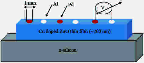
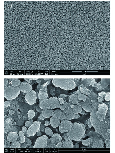
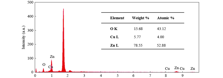
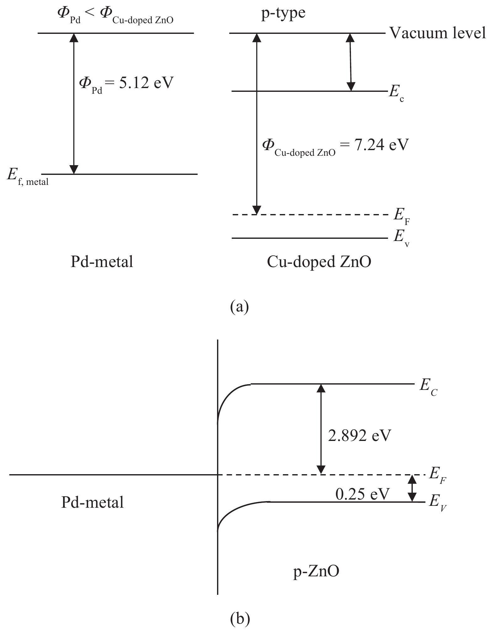
A systematic study of the behaviour of Pd/p-ZnO thin film Schottky diode has been reported. The p-type ZnO thin film with improved stability has been grown on n-type Si by doping ZnO with copper. Seebeck measurement confirmed the p-type nature of Cu-doped ZnO thin film. The X-ray diffraction spectra of the deposited film revealed polycrystalline nature with preferred growth orientation of (101) of ZnO film. The surface morphological study demonstrated the conformal deposition of a thin film over n-Si wafer. The estimated bandgap of Cu-doped p-type ZnO thin film from ellipsometric measurement turns out to be 3.14 eV at 300 K. The measured electrical parameters of the proposed Pd/p-ZnO Schottky diode have also been validated by the results of numerical simulation obtained by using ATLASTM device simulator.


J. Semicond.
2017, 38(10): 104003 doi: 10.1088/1674-4926/38/10/104003

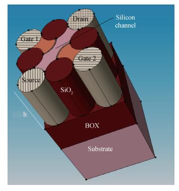
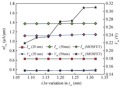
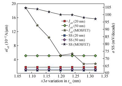
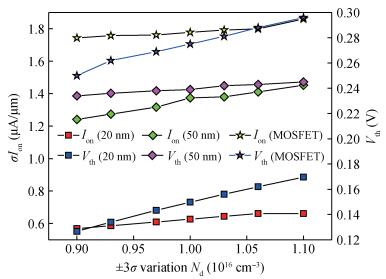
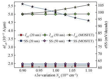
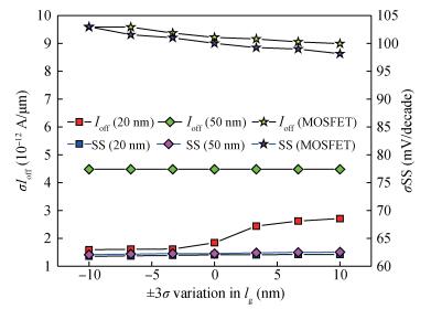
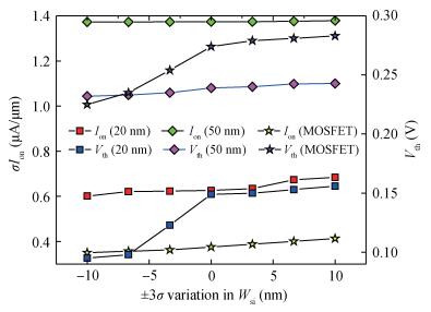
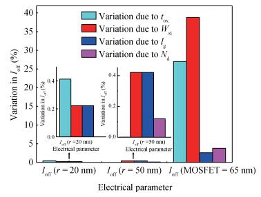
This paper presents an in-depth analysis of junctionless double gate vertical slit FET (JLDG VeSFET) device under process variability. It has been observed that junctionless FETs (JLDG VeSFET) are significantly less sensitive to many process parameter variations due to their inherent device structure and geometric properties. Sensitivity analysis reveals that the slit width, oxide thickness, radius of the device, gate length and channel doping concentration imperceptibly affect the device performance of JLDG VeSFET in terms of variation in threshold voltage, on current, off current and subthreshold slope (Ssub) as compared to its junction based counterpart i.e. MOSFET, because various short channel effects are well controlled in this device. The maximum variation in off current for JLDG VeSFET due to variation in different devices parameters is 5.6% whereas this variation is 38.8% for the MOS junction based device. However, variation in doping concentration in the channel region displays a small deviation in the threshold voltage and on current characteristics of the MOSFET device as compared to JL DG VeSFET.


J. Semicond.
2017, 38(10): 104004 doi: 10.1088/1674-4926/38/10/104004

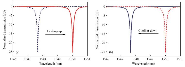
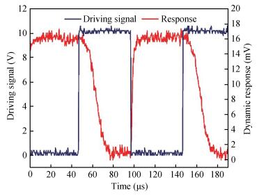
The silicon microring resonator plays an important role in large-scale, high-integrability modern switching matrixes and optical networks, as silicon photonics enables ring resonators of an unprecedented compact size. But as the nature of resonators is their sensitivity to temperature, their performances are vulnerable to being affected by thermal effect. In this paper, we analyze the dominant thermal effects to the application of silicon microring optical switch. On the one hand we theoretically analyze and experimentally measure the thermal crosstalk among adjacent microring optical switches with different distances, and give possible solutions to minimize the affect of thermal crosstalk. On the other hand we analyze and measure the thermooptic dynamic response of microring switch; the experiment shows for the thermal-tuning that the rising edge is around 2μs, and the falling edge is around 35μs. We give the explanation of the asymmetric rise-time and fall-time.


J. Semicond.
2017, 38(10): 104005 doi: 10.1088/1674-4926/38/10/104005

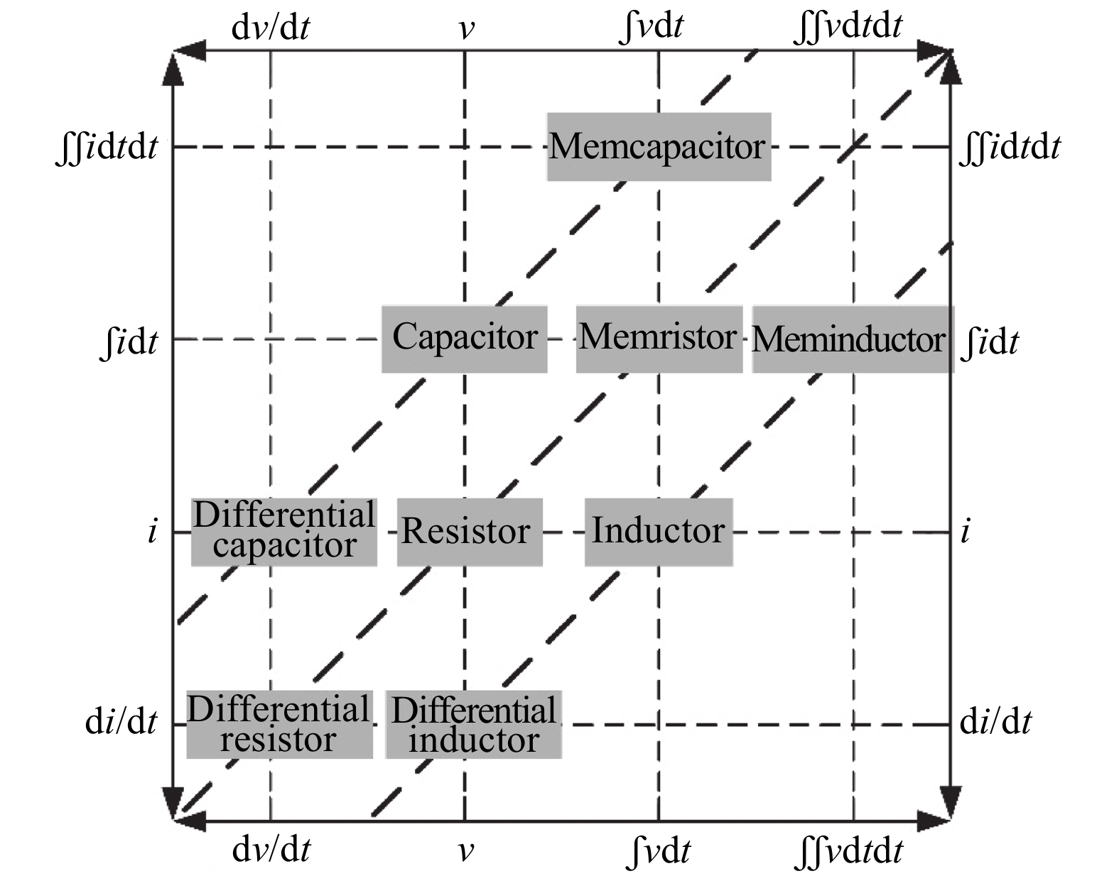
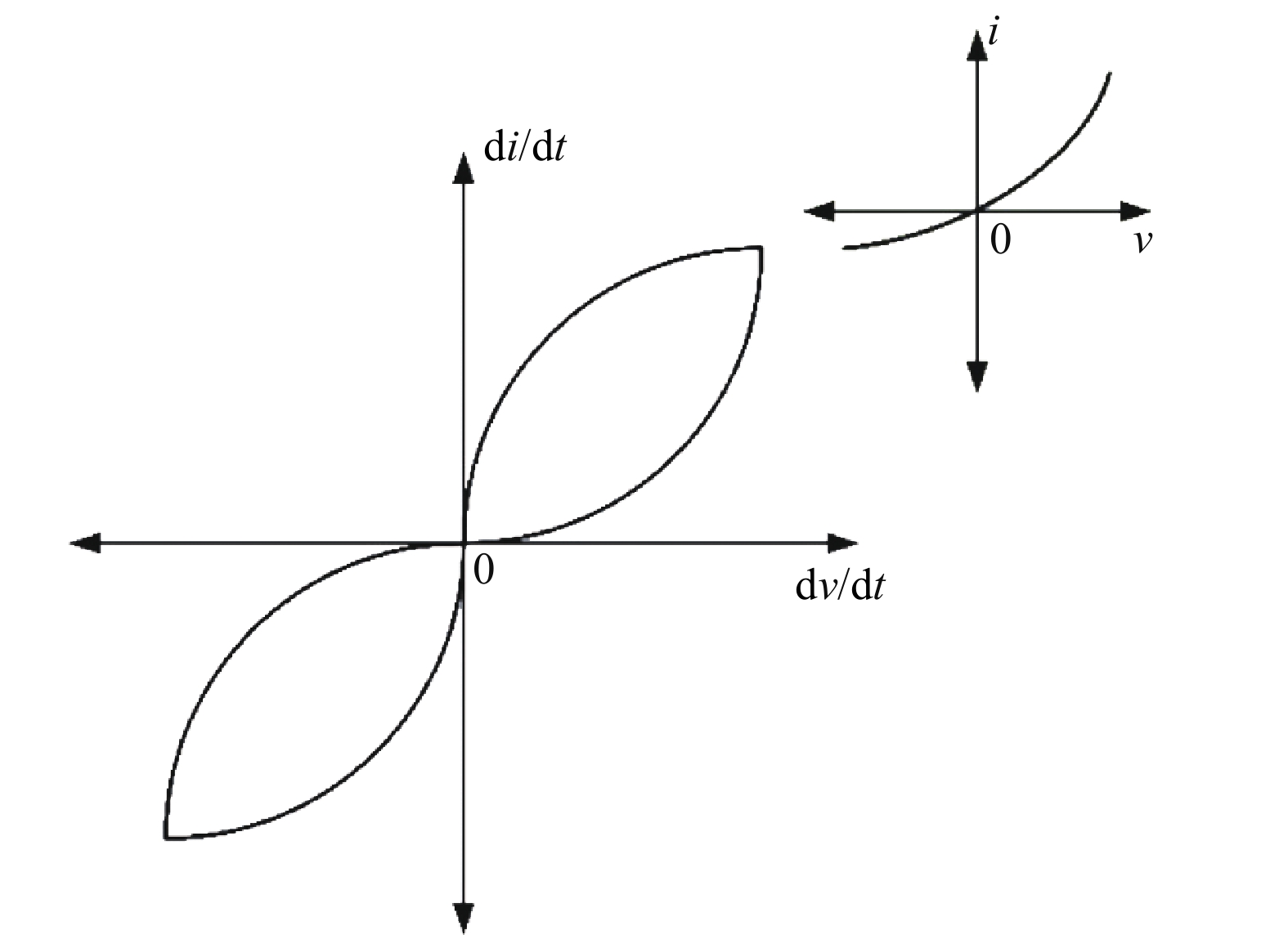
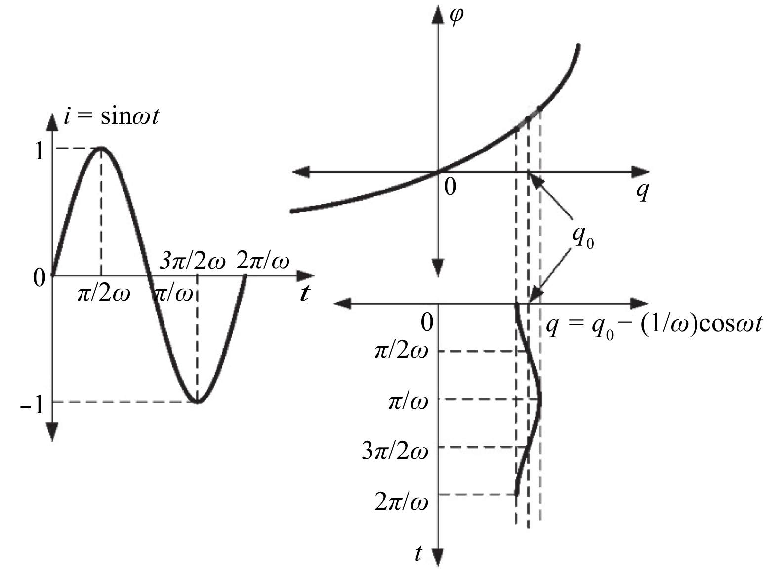
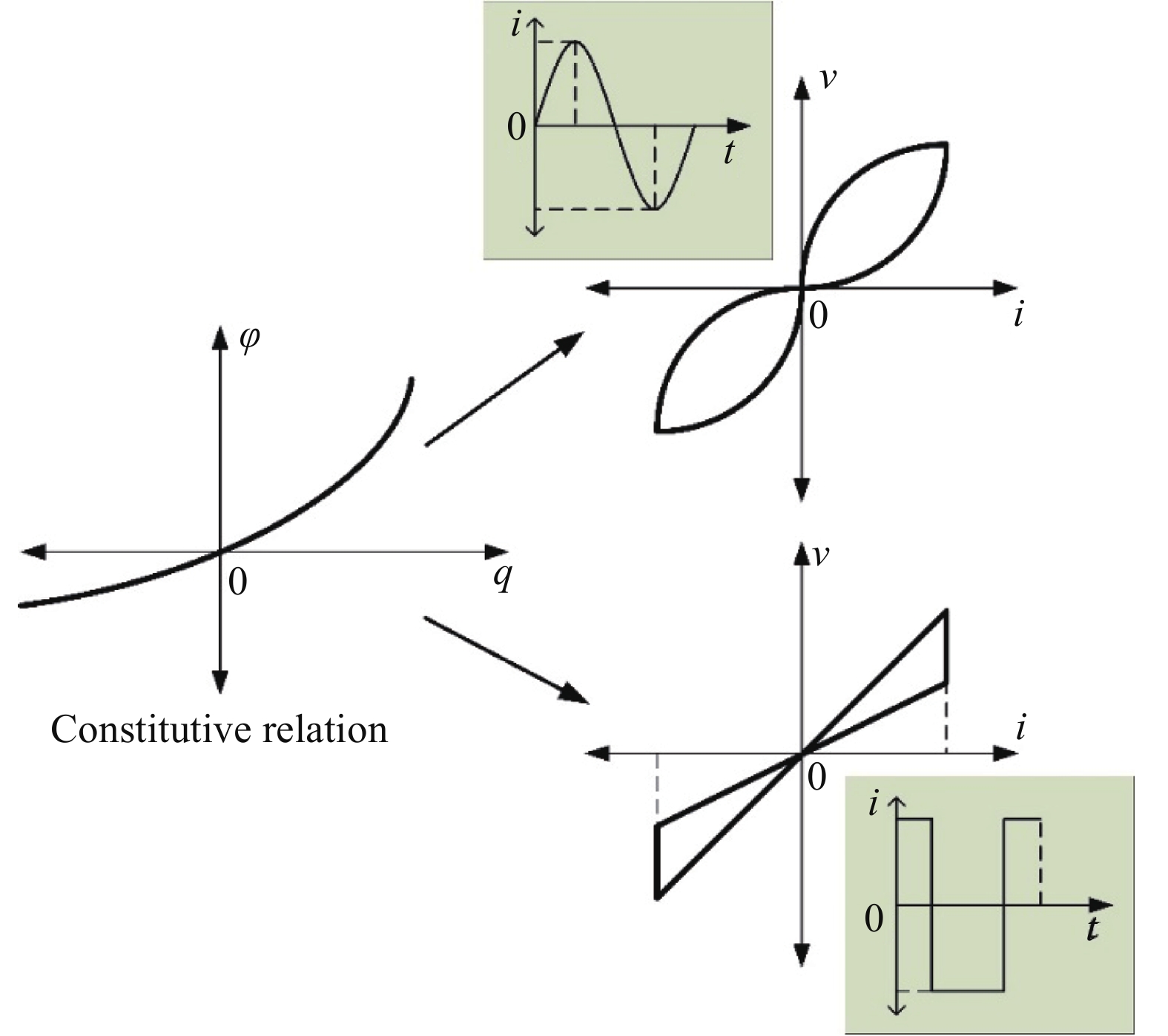
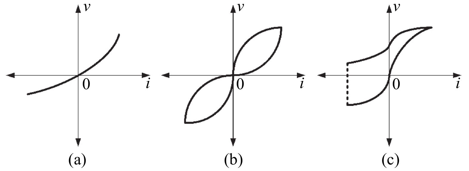
The attractive memristor is interpreted based on its constitutive relation. The memory property of the memristor is explained, along with the explanation on its three fingerprints: (1) Pinched hysteresis loop; (2) Hysteresis lobe area decreases as frequency increases; (3) Pinched hysteresis loop shrinks to a single-valued function at infinite frequency. Where the magnetic flux is in Strukov’s memristor is also introduced. Resistive elements including the memristor are taken as an example to argue that the constitutive relation determines the electrical property of a circuit element and diagram method is used to distinguish different elements in the resistive element series.


J. Semicond.
2017, 38(10): 105006 doi: 10.1088/1674-4926/38/10/105006
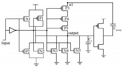
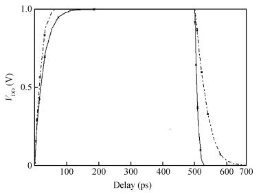
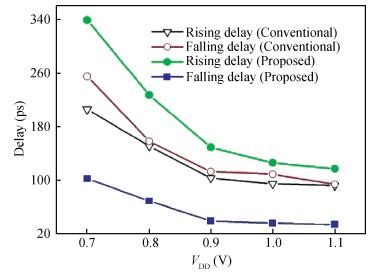
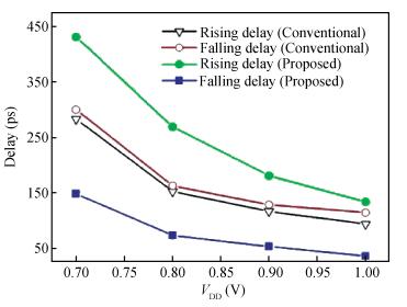
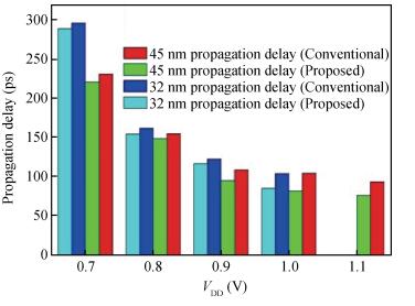
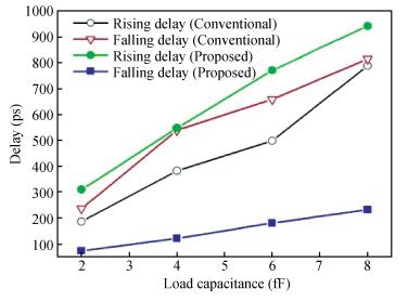
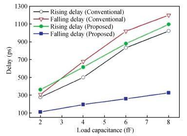
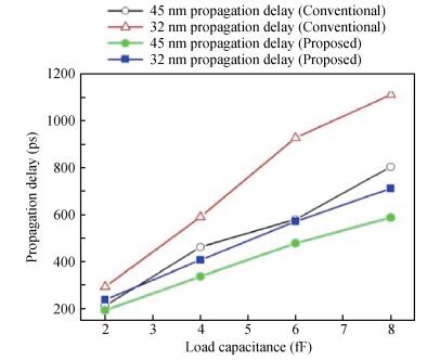
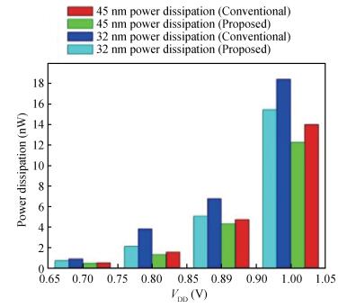
This paper proposes a repeater for boosting the speed of interconnects with low power dissipation. We have designed and implemented at 45 and 32 nm technology nodes. Delay and power dissipation performances are analyzed for various voltage levels at these technology nodes using Spice simulations. A significant reduction in delay and power dissipation are observed compared to a conventional repeater. The results show that the proposed high-speed low-power repeater has a reduced delay for higher load capacitance. The proposed repeater is also compared with LPTG CMOS repeater, and the results shows that the proposed repeater has reduced delay. The proposed repeater can be suitable for high-speed global interconnects and has the capacity to drive large loads.

J. Semicond.
2017, 38(10): 105007 doi: 10.1088/1674-4926/38/10/105007
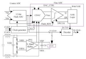
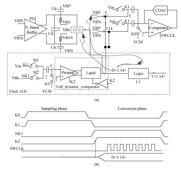
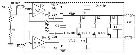
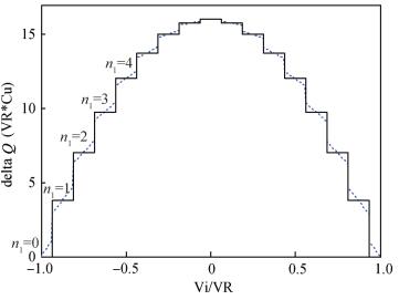
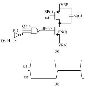
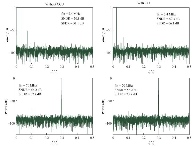
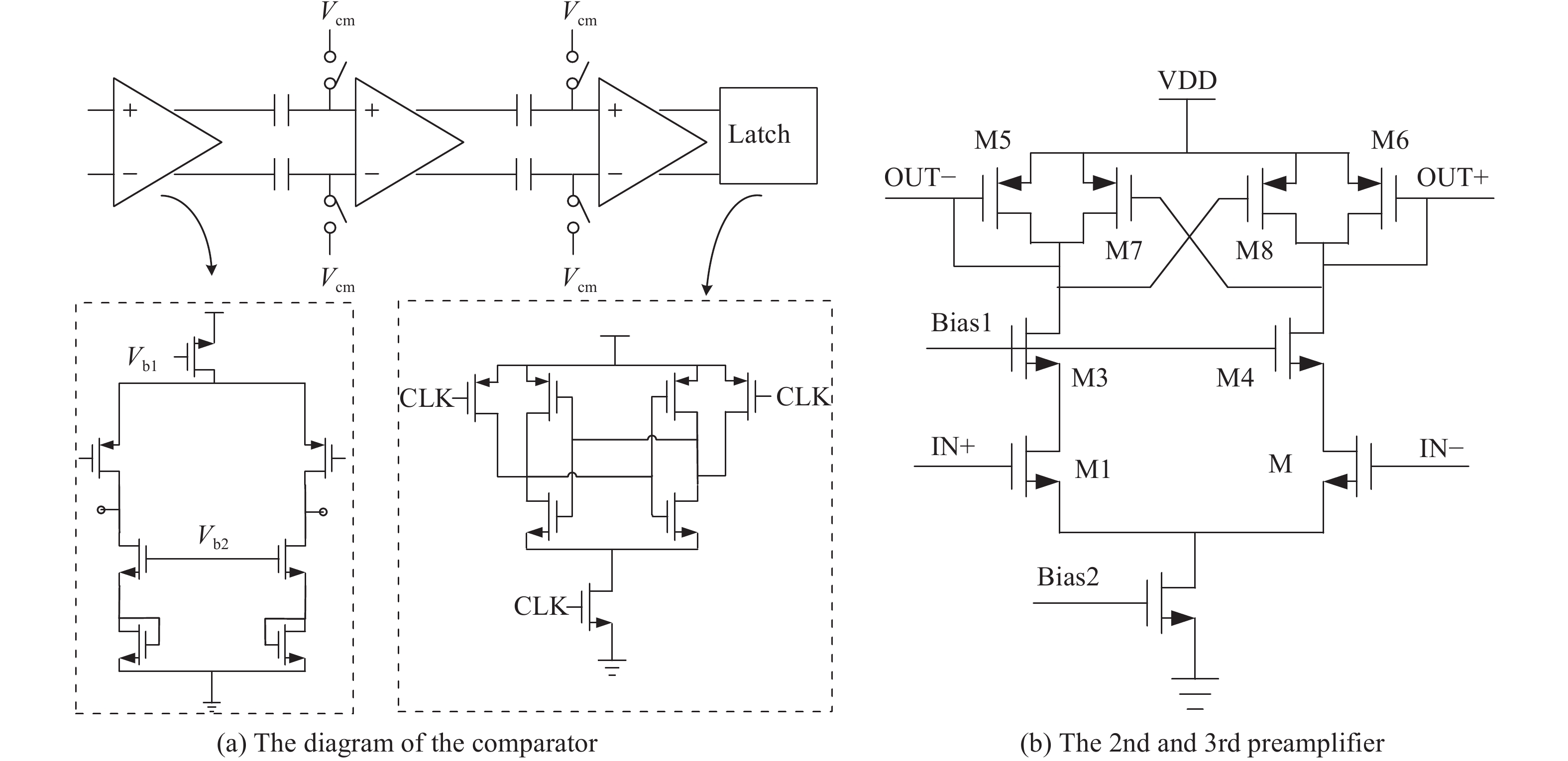
This paper presents an 11-bit 200 MS/s subrange SAR ADC with an integrated reference buffer in 65 nm CMOS. The proposed ADC employs a 3.5-bit flash ADC for coarse conversion, and a compact timing scheme at the flash/SAR boundary to speed up the conversion. The flash decision is used to control charge compensating for the reference voltage to reduce its input-dependent fluctuation. Measurement results show that the fabricated ADC has achieved significant improvement by applying the reference charge compensation. In addition, the ADC achieves a maximum signal-to-noise-and-distortion ratio of 59.3 dB at 200 MS/s. It consumes 3.91 mW from a 1.2 V supply, including the reference buffer.


J. Semicond.
2017, 38(10): 105008 doi: 10.1088/1674-4926/38/10/105008
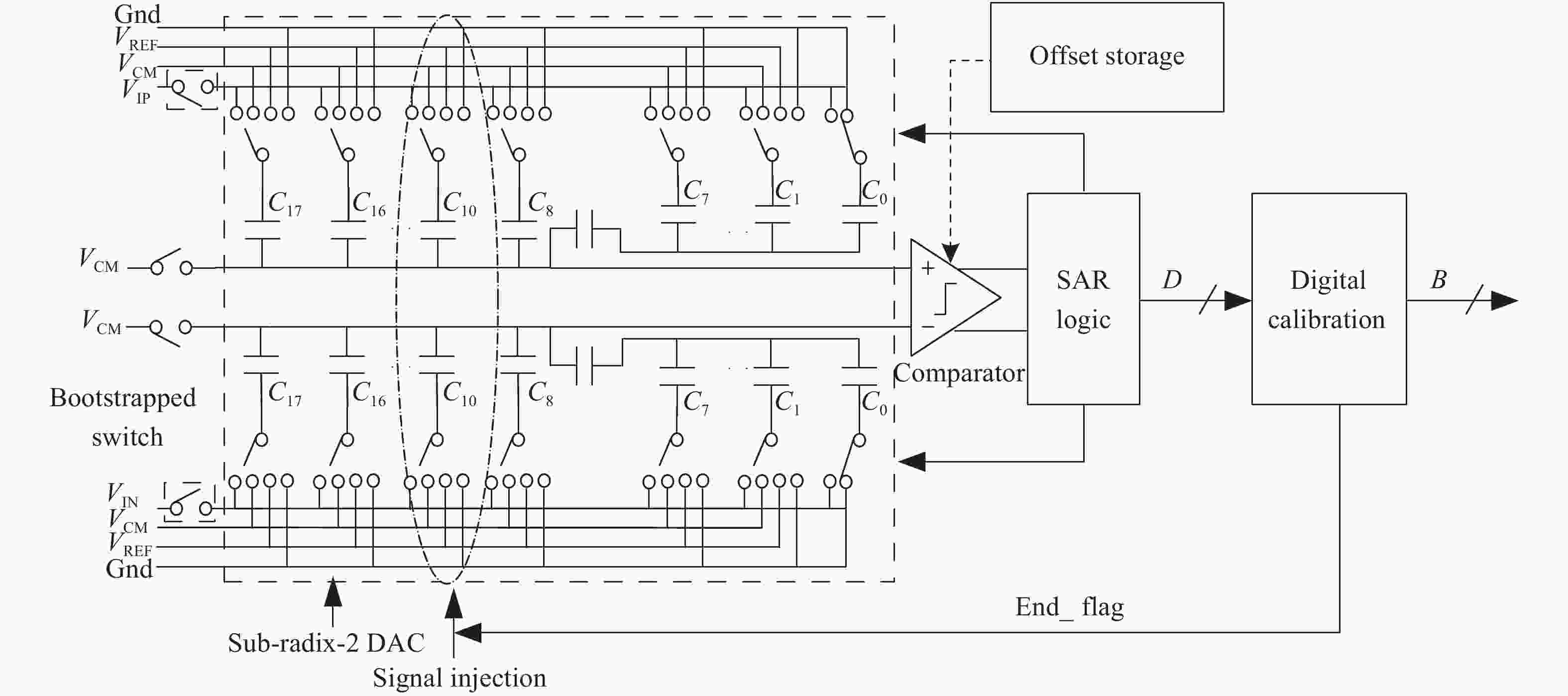
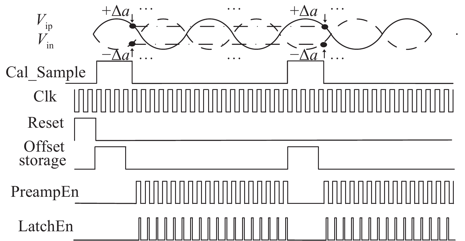
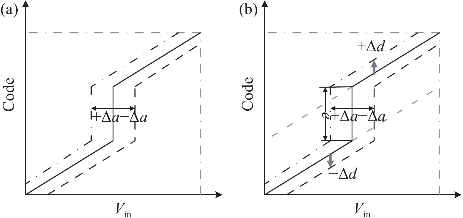
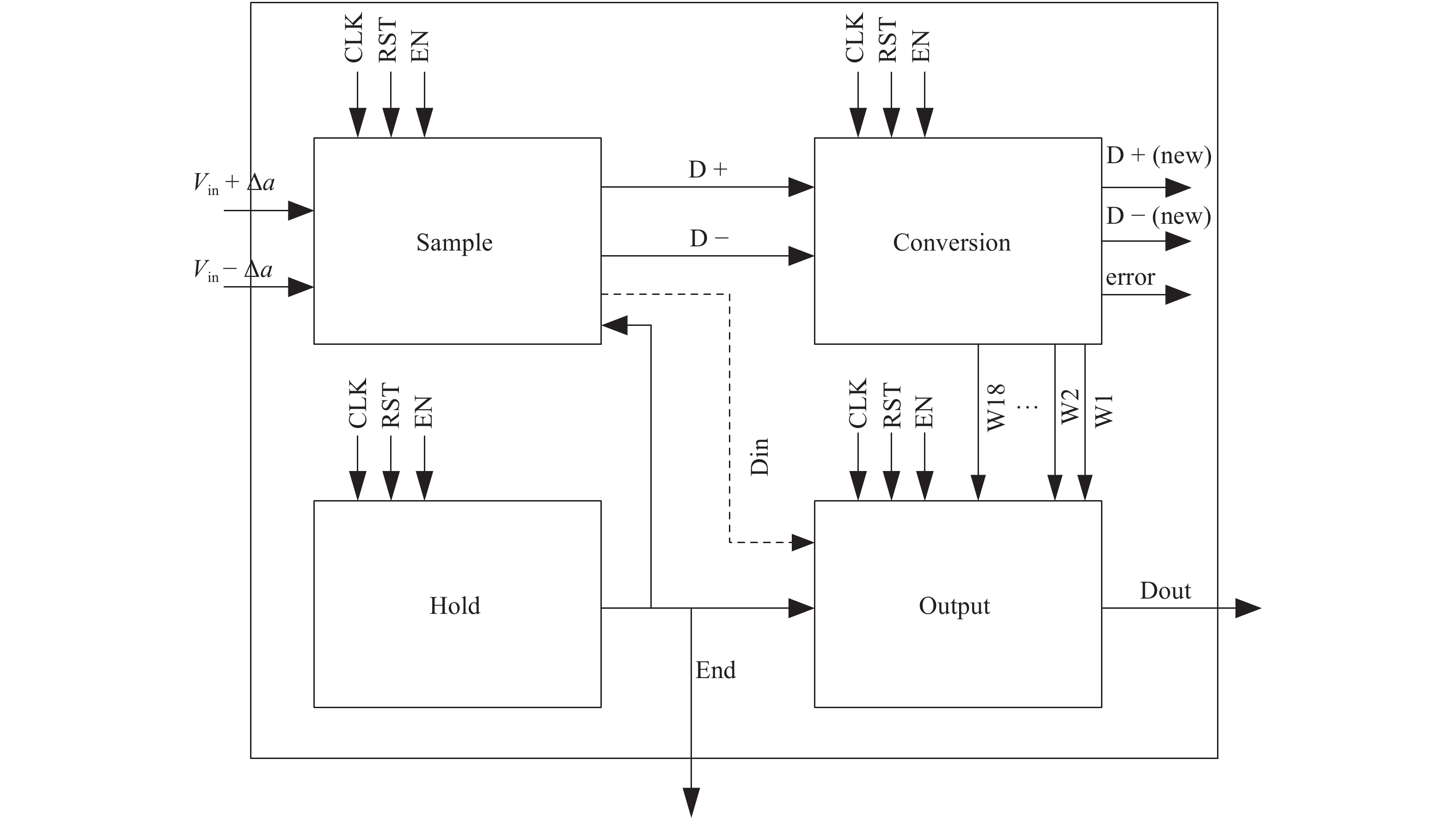
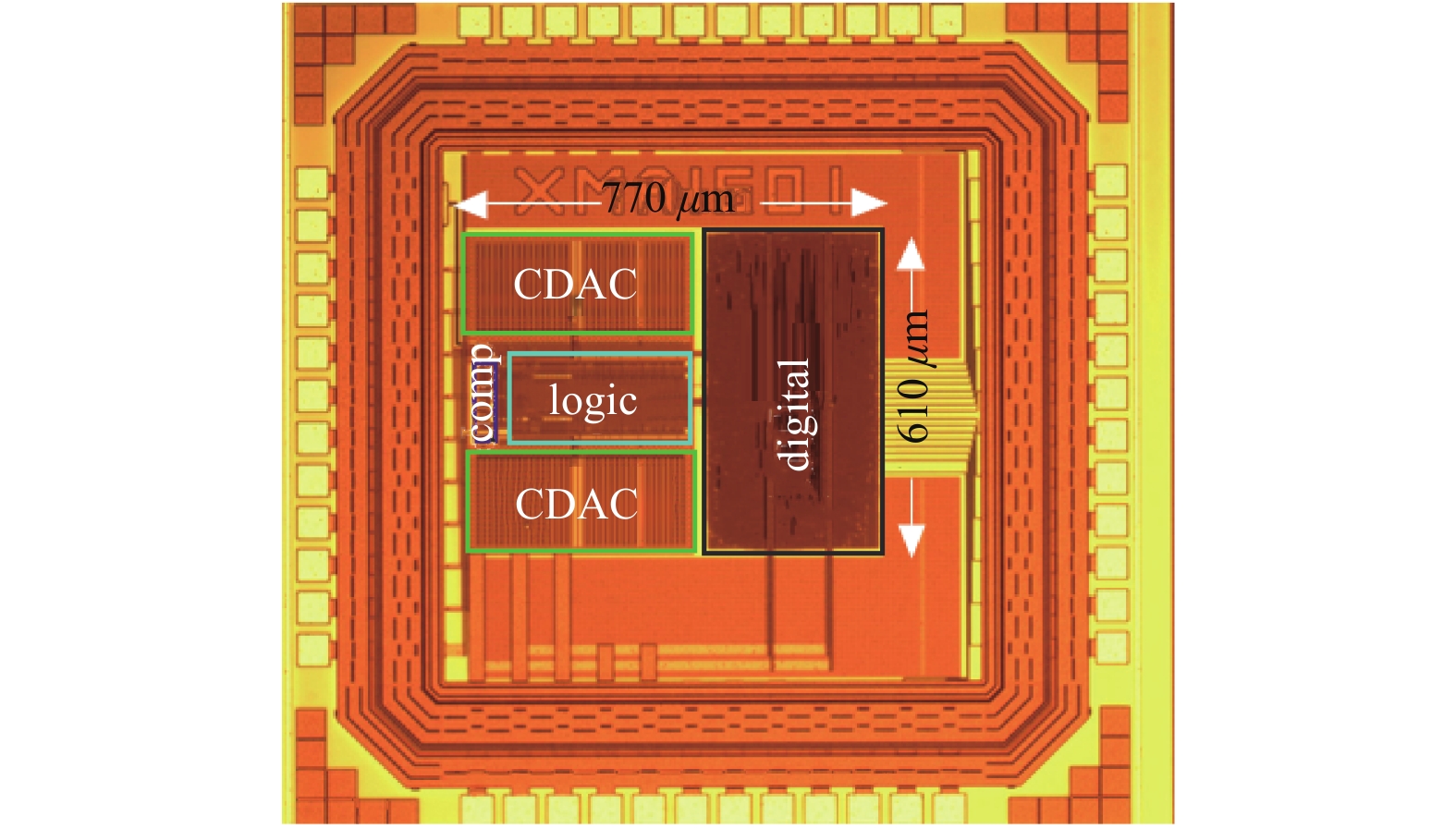
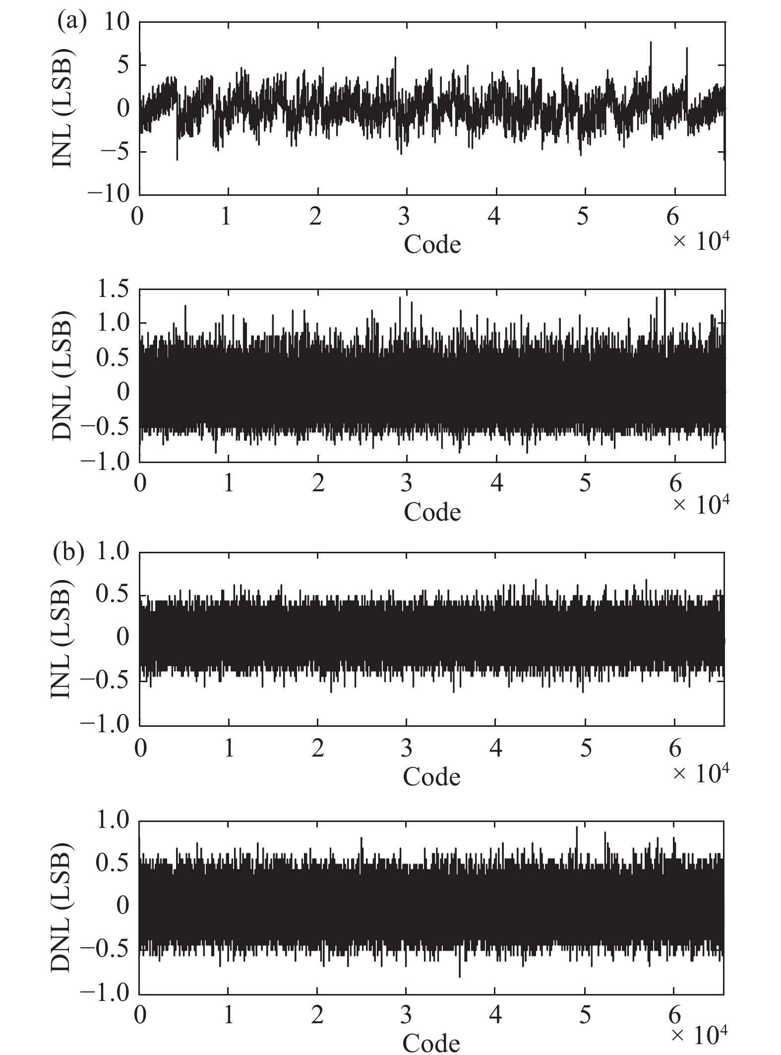
This paper proposes a high-resolution successive-approximation register (SAR) analog-to-digital converter (ADC) with sub-2 radix split-capacitor array architecture. The built-in redundancy of sub-2 radix architecture provides additional information in the digital calibration based on offset double injection. The calibration method is simple in structure and fast in convergence. The correction of errors in each bit is independent of those in the previous bit. A split-capacitor array is used to reduce the total capacitance especially in a high-resolution SAR ADC. An offset signal is injected by the switching scheme of capacitor array to minimize the hardware overhead. The prototype of 0.18 μm CMOS process obtains 14.46 bit ENOB and 95.65 dB SFDR after calibration. With calibration, the INL and DNL are −0.813/0.938 and −0.625/0.688, respectively.


J. Semicond.
2017, 38(10): 105009 doi: 10.1088/1674-4926/38/10/105009

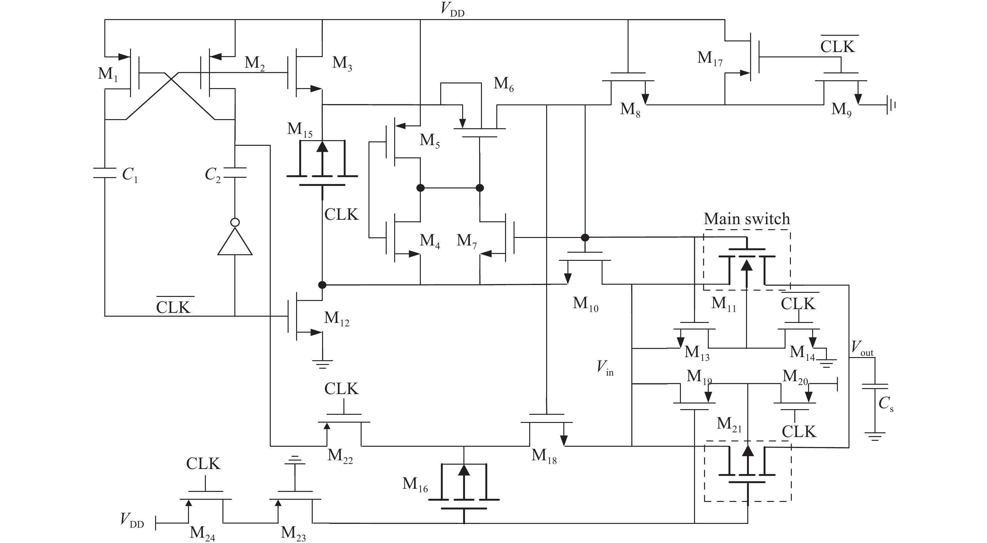
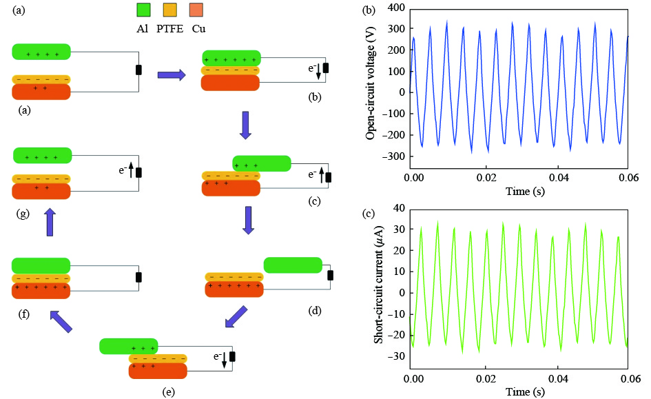
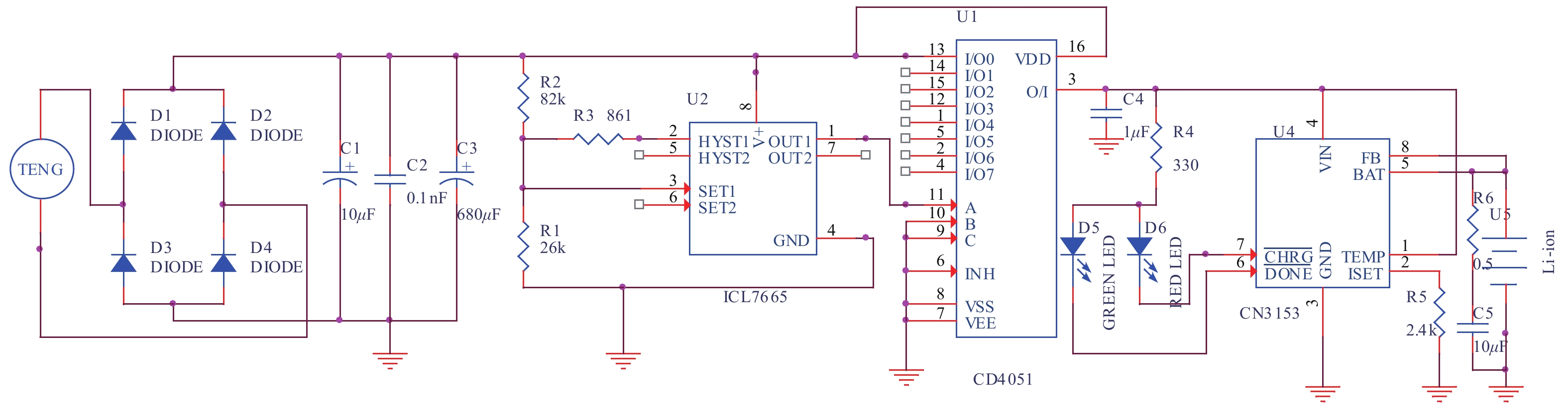
For most triboelectric nanogenerators (TENGs), the electric output should be a short AC pulse, which has the common characteristic of high voltage but low current. Thus it is necessary to convert the AC to DC and store the electric energy before driving conventional electronics. The traditional AC voltage regulator circuit which commonly consists of transformer, rectifier bridge, filter capacitor, and voltage regulator diode is not suitable for the TENG because the transformer’s consumption of power is appreciable if the TENG output is small. This article describes an innovative design of an interface circuit for a triboelectric nanogenerator that is transformerless and easily integrated. The circuit consists of large-capacity electrolytic capacitors that can realize to intermittently charge lithium-ion batteries and the control section contains the charging chip, the rectifying circuit, a comparator chip and switch chip. More important, the whole interface circuit is completely self-powered and self-controlled. Meanwhile, the chip is widely used in the circuit, so it is convenient to integrate into PCB. In short, this work presents a novel interface circuit for TENGs and makes progress to the practical application and industrialization of nanogenerators.


J. Semicond.
2017, 38(10): 105010 doi: 10.1088/1674-4926/38/10/105010
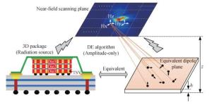
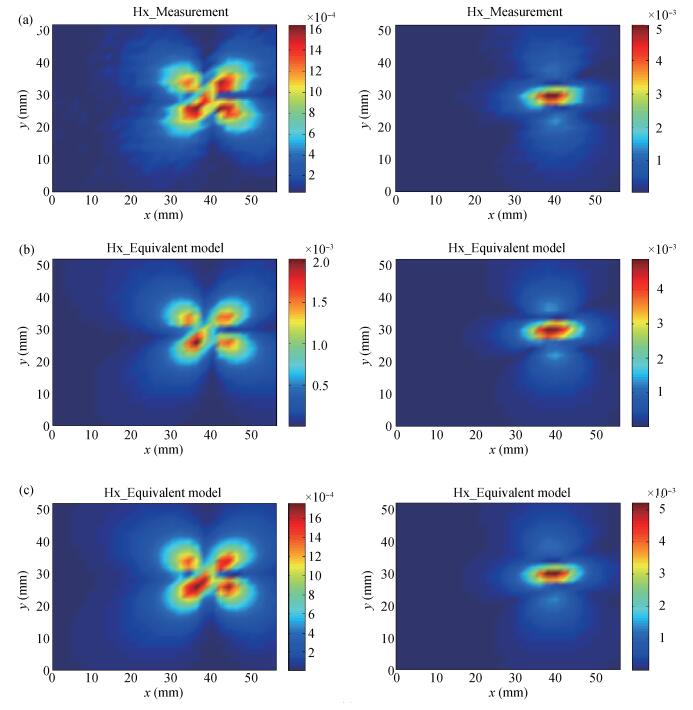
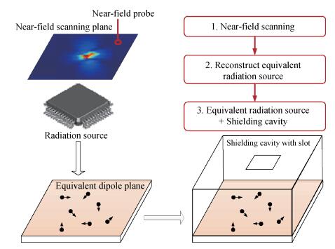
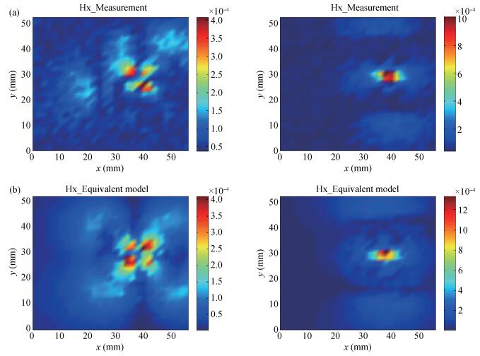
An equivalent radiation source method is proposed to characterize electromagnetic emission and interference of complex three dimensional integrated circuits (IC) in this paper. The method utilizes amplitude-only near-field scanning data to reconstruct an equivalent magnetic dipole array, and the differential evolution optimization algorithm is proposed to extract the locations, orientation and moments of those dipoles. By importing the equivalent dipoles model into a 3D full-wave simulator together with the victim circuit model, the electromagnetic interference issues in mixed RF/digital systems can be well predicted. A commercial IC is used to validate the accuracy and efficiency of this proposed method. The coupled power at the victim antenna port calculated by the equivalent radiation source is compared with the measured data. Good consistency is obtained which confirms the validity and efficiency of the method.


J. Semicond.
2017, 38(10): 106001 doi: 10.1088/1674-4926/38/10/106001
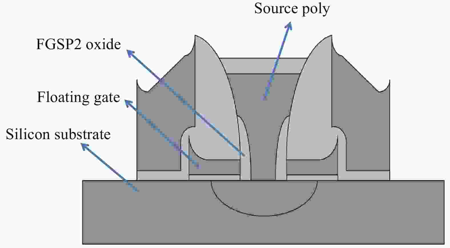
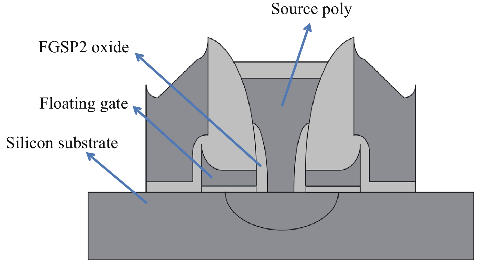
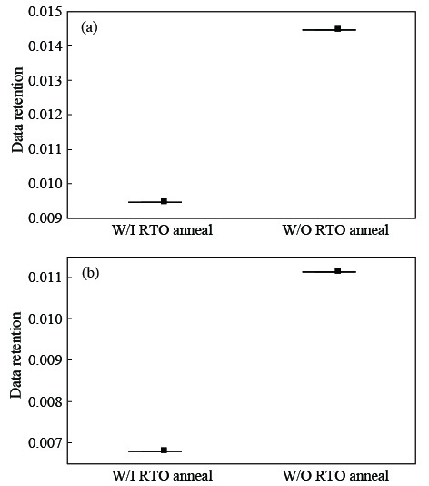
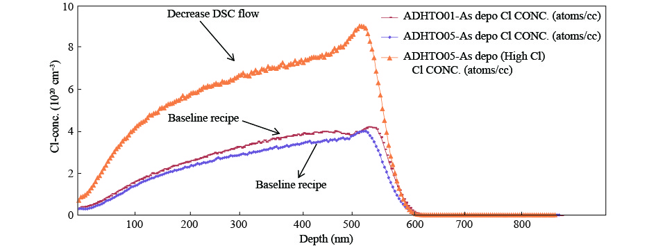
Data retention is one of the most important reliability characteristics of split-gate flash. Therefore, many efforts were made to improve data retention of split-gate flash. By experiments, it was found that higher chlorine concentration produced in FGSP2 oxide deposition can induce worse data retention. Thus, reducing chlorine concentration is an effective approach to improve data retention for split-gate flash product. Additional RTO annealing between FGSP2 oxide deposition and FGSP2 etching could reduce chlorine concentration, and improve FGSP2 oxide film quality, and then get better data retention.