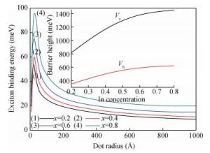
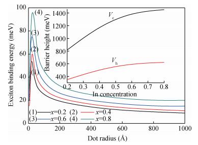
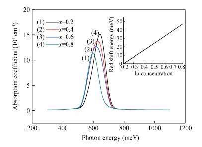
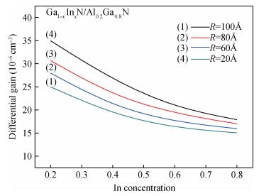
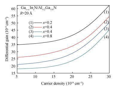
Electronic and optical properties are obtained with the increase in indium alloy content (x) in a Ga1-xInxN/Al0.2Ga0.8N quantum dot. The barrier height with the different In alloy contents is applied to acquire the confinement potentials. The results are obtained taking into consideration geometrical confinement effect. The optical absorption coefficient with the photon energy is observed in a Ga1-xInxN/Al0.2Ga0.8N quantum dot. The optical output with the injection current density and the threshold optical pump intensity for various In alloy contents are studied. The differential gain as functions of indium alloy content, charge density and the dot radii in the Ga1-xInxN/Al0.2Ga0.8N quantum dot are investigated. The exciton binding energy is calculated in order to obtain the exciton density, the optical gain and the threshold current density in the Ga1-xInxN/Al0.2In0.8N quantum dot. The results show that the red shift energy with an increase in In alloy content is found and the differential gain increases with the charge carrier density.

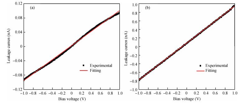
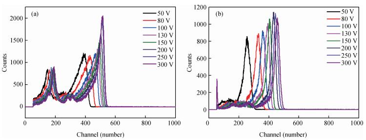
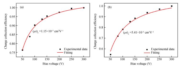
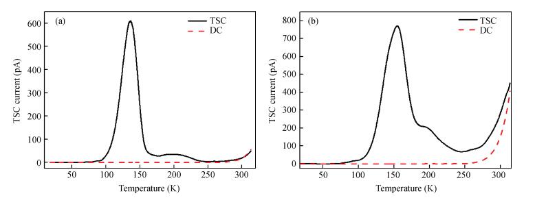
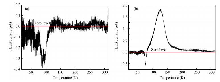
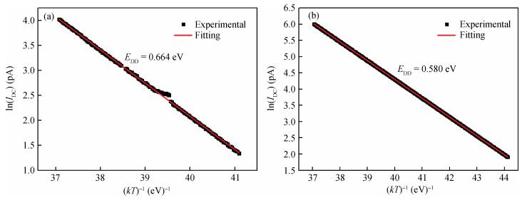
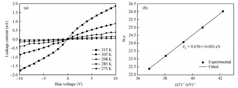
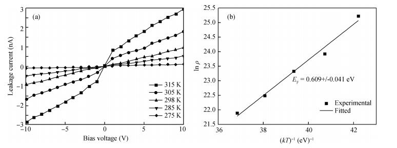
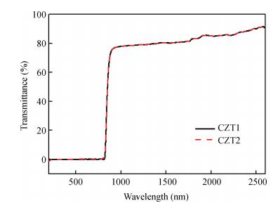
The deep-level defects of CdZnTe (CZT) crystals grown by the modified vertical Bridgman (MVB) method act as trapping centers or recombination centers in the band gap, which have significant effects on its electrical properties. The resistivity and electron mobility-lifetime product of high resistivity Cd0.9Zn0.1Te wafer marked CZT1 and low resistivity Cd0.9Zn0.1Te wafer marked CZT2 were tested respectively. Their deep-level defects were identified by thermally stimulated current (TSC) spectroscopy and thermoelectric effect spectroscopy (TEES) respectively. Then the trap-related parameters were characterized by the simultaneous multiple peak analysis (SIMPA) method. The deep donor level (EDD)dominating dark current was calculated by the relationship between dark current and temperature. The Fermi-level was characterized by current-voltage measurements of temperature dependence. The width of the band gap was characterized by ultraviolet-visible-infrared transmittance spectroscopy. The results show the traps concentration and capture cross section of CZT1 are lower than CZT2, so its electron mobility-lifetime product is greater than CZT2. The Fermi-level of CZT1 is closer to the middle gap than CZT2. The degree of Fermi-level pinned by EDD of CZT1 is larger than CZT2. It can be concluded that the resistivity of CZT crystals increases as the degree of Fermi-level pinned near the middle gap by the deep donor level enlarges.


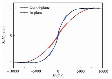
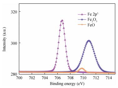
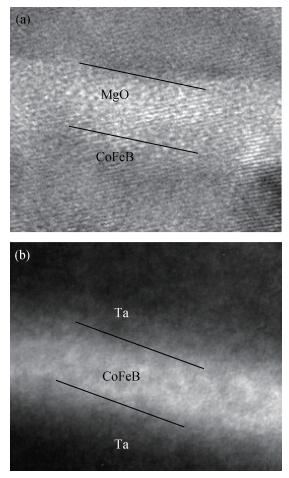
The mechanism of perpendicular magnetic anisotropy (PMA) in a MgO-based magnetic tunnel junction (MTJ) has been studied in this article. By comparing the magnetic properties and elementary composition analysis for different CoFeB-based structures, such as Ta/CoFeB/MgO, Ta/CoFeB/Ta and Ru/CoFeB/MgO structures, it is found that a certain amount of Fe-oxide existing at the interface of CoFeB/MgO is helpful to enhance the PMA and the PMA is originated from the interface of CoFeB/MgO. In addition, Ta film plays an important role to enhance the PMA in Ta/CoFeB/MgO structure.


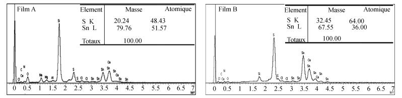
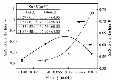
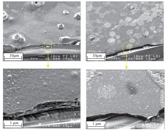
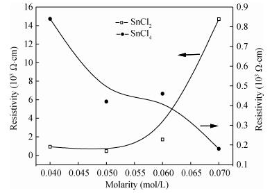
Thin films of SnSx, semiconductors, have been successfully synthesized by ultrasonic spray pyrolysis technique, using two precursors namely:tin (Ⅱ) chloride and tin (Ⅳ) chloride, respectively. The solutions were prepared by the dilution of different Sn molarities of the two precursors separately. The precursor molarities were varied from 0.04 to 0.07 mol/L, whereas that of S was fixed at 0.1 mol/L. The present work focuses on the effect of the different precursor's molarities on the nature and the properties of the prepared thin films in order to optimize the growth conditions. X-ray diffraction analysis reveals that the precursor's molarities alter the grain size of the prepared films, which varied from 8 to 14 nm and from 12 to 16 nm, according to the used precursor. The films analysis by SEM, shows that the SnS2 films are more dense and smooth than the SnS films. The composition of the elements is analysed with an EDX spectrometer, and the obtained result for Msn D 0:07 mol/L indicates that the atomic ratio of Sn to S is 51.57:48.43 and 36:64 for films synthesized from the first and second precursors respectively. Electrical measurements show that the conductivity behavior depends on the used precursors and their molarities.


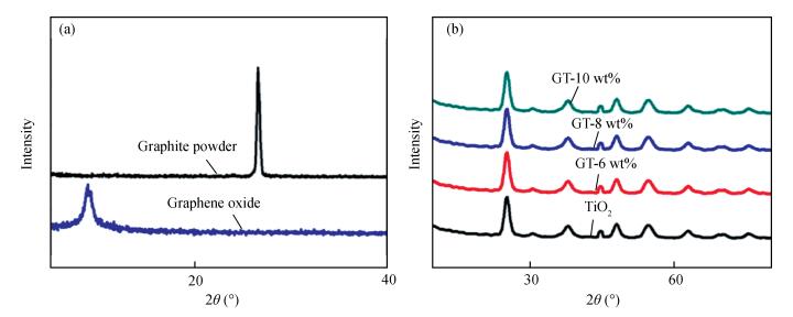
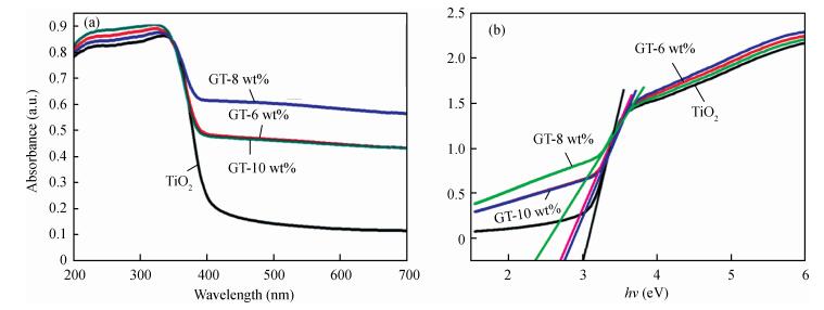
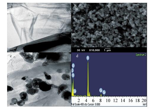
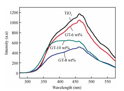
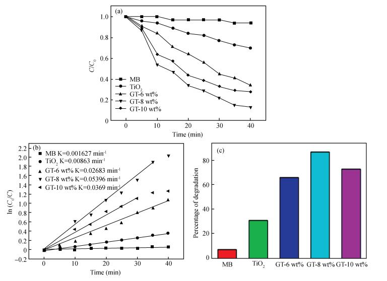
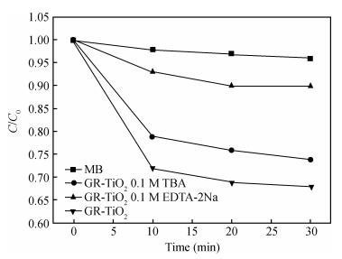
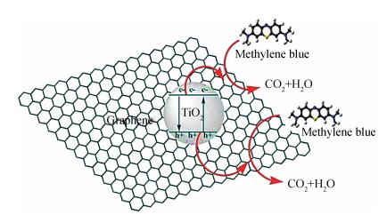
In this paper an improvement in the photocatalytic performance of TiO2 was carried out via hybridizing with graphene. Graphene-TiO2 (GR-TiO2)nanocomposites with different weight addition ratios of graphene oxide (GO) have been prepared via a facile microwave irradiation of GO and tetrabutyl titanate in isopropyl alcohol. Raman spectroscopy (RS), X-ray diffraction (XRD), scanning electron microscopy (SEM), transmission electron microscopy (TEM), UV-visible spectroscopy (UV-vis), Fourier transform infrared spectra (FTIR), energy dispersive X-ray spectroscopy (EDX) and photoluminescence spectra (PL) are employed to determine the properties of the samples. Microwave irradiation can heat the reactant to a higher temperature in a short time, simultaneously GO is reduced to graphene and TiO2 nanoparticles grown on the surface of GR. GR-TiO2 nanocomposites synthesized via this approach have efficient electron conductivity in GR, resulting in a reduced electron-hole recombination rate. Among the synthesized nanocomposites, GT-8wt% exhibited the best photocatalytic activity toward photocatalytic degradation of MB. Our current work provides a new insight for the fabrication of GR-TiO2 nanocomposites within a short reaction time and also explains the mechanism of photocatalysis employing radical and hole scavengers.


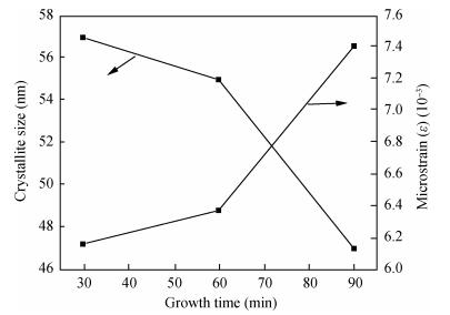
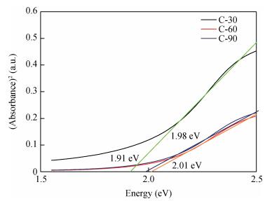
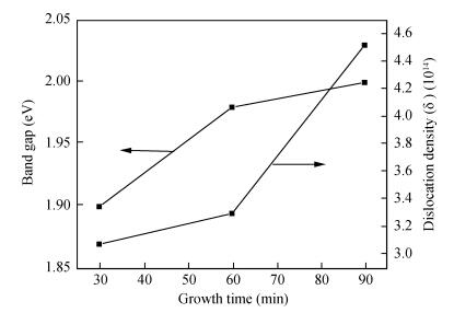
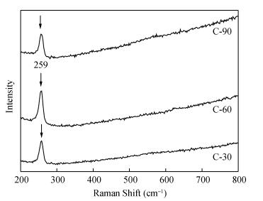
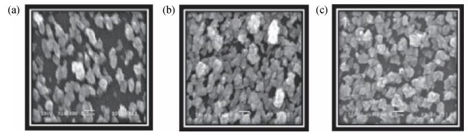
Copper selenide (Cu3Se2)thin films have been synthesized with Se as the precursor in aqueous solution by chemical bath deposition technique at room temperature. We have investigated the influence of the growth time ranging from 30 to 90 min on structural, optical and electrical properties of Cu3Se2 thin films. The as-grown film at 60 min exhibits a tetragonal structure and is (101) oriented. The maximum value of crystal size D= 55 nm is attained for Cu3Se2 films grown at 60 min. The Raman spectrum reveals a pronounced peak at 259 cm-1, which is assigned to vibrational (stretching) modes from the covalent Se-Se bonds. The optical band gap energy is 1.91 to 2.01 eV with growth time increased from 30 to 90 min. The scanning electron microscopy (SEM) study reveals that the grains are uniform and spread over the entire surface of the substrate of the film at 60 min. The Hall effect study reveals that the film exhibits p-type conductivity. The synthesized film showed good absorbance in the visible region which signifies that synthesized Cu3Se2 films can be suitable as a sensitized material in semiconductor sensitized solar cells.


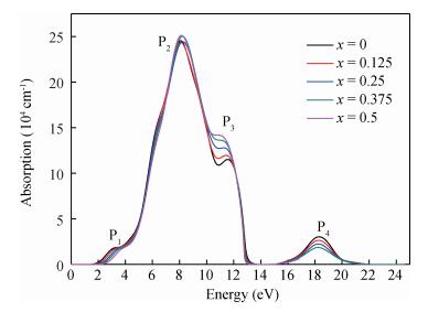
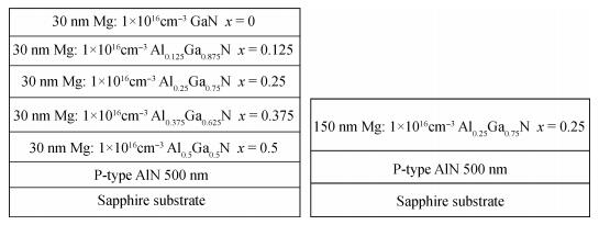
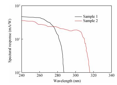
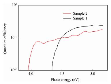
To theoretically research the influence of a varied Al component on the active layer of AlGaN photocathodes, the first principle based on density functional theory is used to calculate the formation energy and band structure of AlxGa1-xN with x at 0, 0.125, 0.25, 0.325, and 0.5. The calculation results show that the formation energy declines along with the Al component rise, while the band gap is increasing with Al component increasing. AlxGa1-x with x at 0, 0.125, 0.25, 0.325, and 0.5 are direct band gap semiconductors, and their absorption coefficient curves have the same variation tendency. For further study, we designed two kinds of reflection-mode AlGaN photocathode samples. Sample 1 has an AlxGa1-x active layer with varied Al component ranging from 0.5 to 0 and decreasing from the bulk to the surface, while sample 2 has an AlxGa1-x active layer with the fixed Al component of 0.25. Using the multi-information measurement system, we measured the spectral response of the activated samples at room temperature. Their photocathode parameters were obtained by fitting quantum efficiency curves. Results show that sample 1 has a better spectral response than sample 2 at the range of short-wavelength. This work provides a reference for the structure design of the AlGaN photocathode.

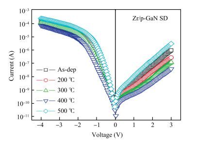
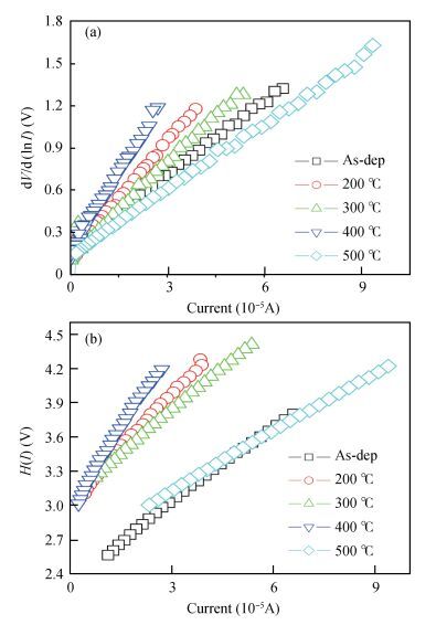
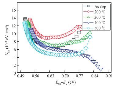
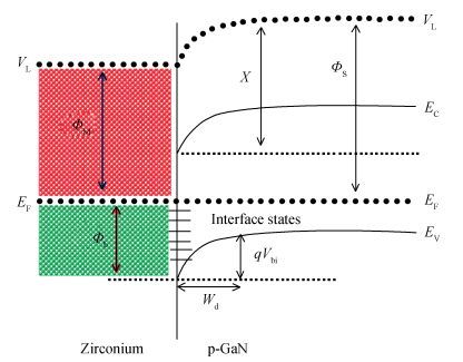
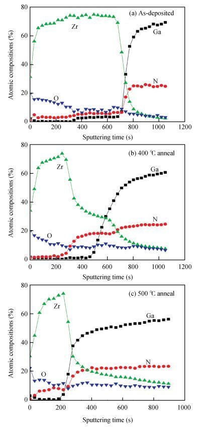
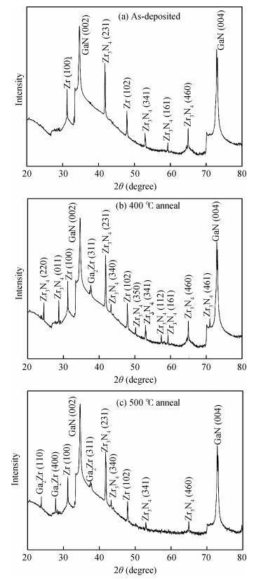
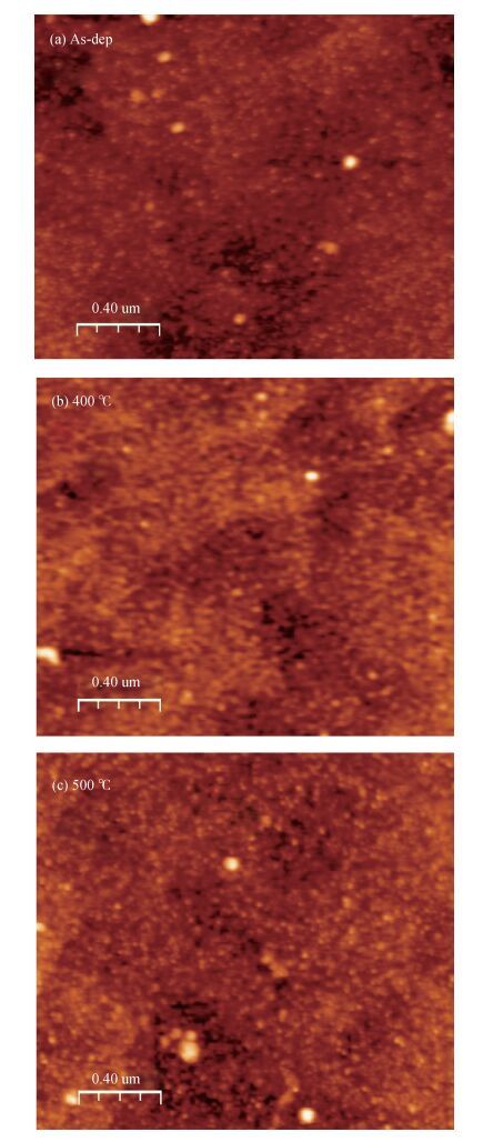
The Schottky barrier junction parameters and structural properties of Zr/p-GaN Schottky diode are explored at various annealing temperatures. Experimental analysis showed that the barrier height (BH) of the Zr/pGaN Schottky diode increases with annealing at 400℃ (0.92 eV (I-V)/1.09 eV (C-V)compared to the asdeposited one (0.83 eV (I-V)/0.93 eV (C-V). However, the BH decreases after annealing at 500℃. Also, at different annealing temperatures, the series resistance and BH are assessed by Cheung's functions and their values compared. Further, the interface state density (NSS)of the diode decreases after annealing at 400℃ and then somewhat rises upon annealing at 500℃. Analysis reveals that the maximum BH is obtained at 400℃, and thus the optimum annealing temperature is 400℃ for the diode. The XPS and XRD analysis revealed that the increase in BH may be attributed to the creation of Zr-N phases with increasing annealing up to 400℃. The BH reduces for the diode annealed at 500℃, which may be due to the formation of Ga-Zr phases at the junction. The AFM measurements reveal that the overall surface roughness of the Zr film is quite smooth during rapid annealing process.

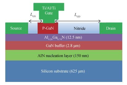
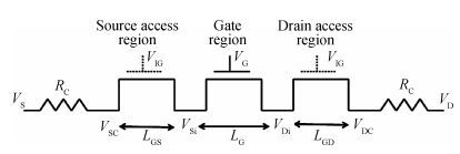
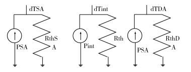
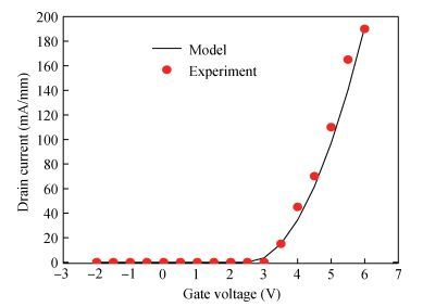
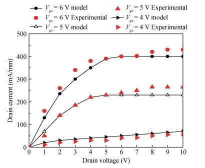
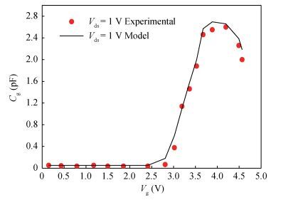
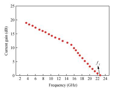
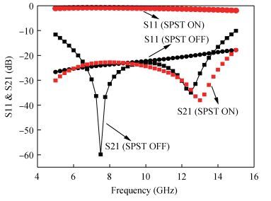
An enhancement mode p-GaN gate AlGaN/GaN HEMT is proposed and a physics based virtual source charge model with Landauer approach for electron transport has been developed using Verilog-A and simulated using Cadence Spectre, in order to predict device characteristics such as threshold voltage, drain current and gate capacitance. The drain current model incorporates important physical effects such as velocity saturation, short channel effects like DIBL (drain induced barrier lowering), channel length modulation (CLM), and mobility degradation due to self-heating. The predicted Id-Vds, Id-Vgs, and C-V characteristics show an excellent agreement with the experimental data for both drain current and capacitance which validate the model. The developed model was then utilized to design and simulate a single-pole single-throw (SPST) RF switch.

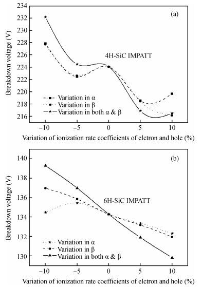
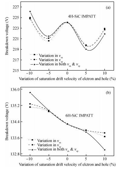
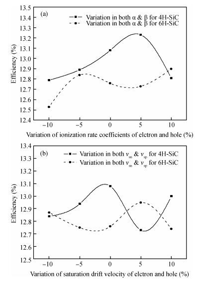
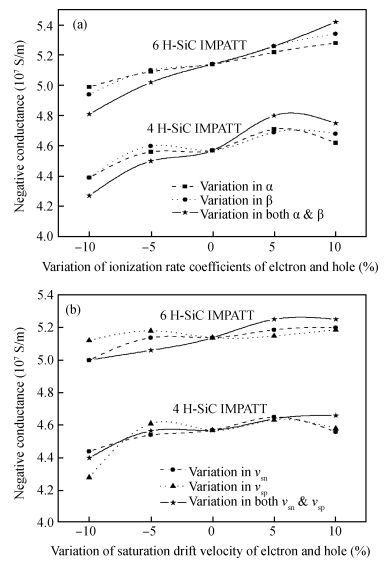
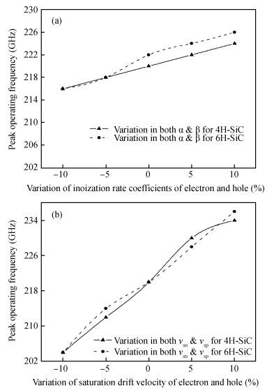
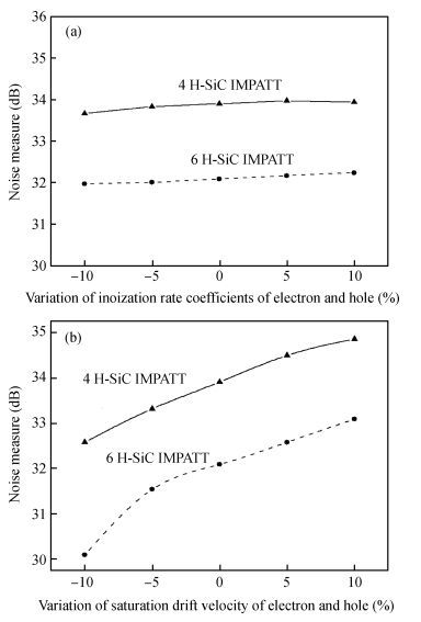
Ionization rate coefficients and saturation drift velocities for electrons and holes are the vital material parameters in determining the performance of an IMPATT diode. We have performed a sensitivity analysis of the millimeter wave characteristics of 4H-SiC and 6H-SiC IMPATT diodes with reference to the above mentioned material data and an operating frequency of 220 GHz. The effect of a small variation in the ionization rate and drift velocity on the device characteristics like break down voltage, efficiency, noise measure and power output has been presented here.
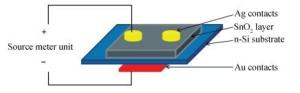
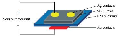
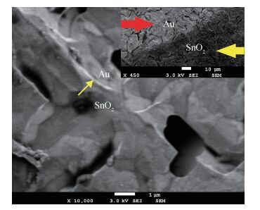
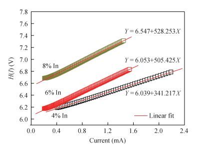
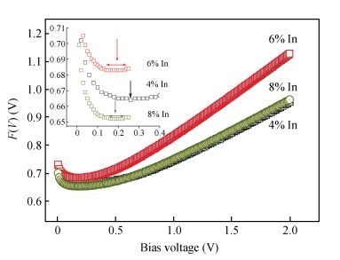
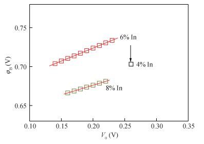
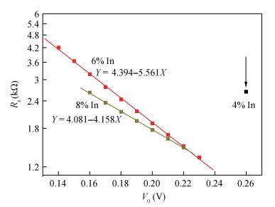
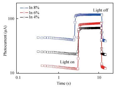
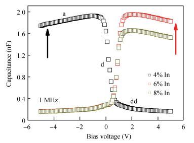
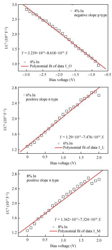
Control of the electronic parameters on a novel metal-oxide-semiconductor (MOS) diode by indium doping incorporation is emphasized and investigated. The electronic parameters, such as ideality factor, barrier height (BH), series resistance, and charge carrier density are extracted from the current-voltage (I-V) and the capacitance-voltage (C-V) characteristics. The properties of the MOS diode based on 4%, 6% and 8% indium doped tin oxide are largely studied. The Ag/SnO2/nSi/Au MOS diode is fabricated by spray pyrolysis route, at 300℃ from the In-doped SnO2 layer. This was grown onto n-type silicon and metallic (Au) contacts which were made by thermal evaporation under a vacuum@10-5 Torr and having a thickness of 120 nm and a diameter of 1 mm. Determined by the Cheung-Cheung approximation method, the series resistance increases (334-534 Ω)with the In doping level while the barrier height (BH) remains constant around 0.57 V. The Norde calculation technique gives a similar BH value of 0.69 V but the series resistance reaches higher values of 5500 Ω. The indium doping level influences on the characteristics of Ag/SnO2:In/Si/Au MOS diode while the 4% indium level causes the capacitance inversion and the device turns into p-type material.


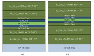
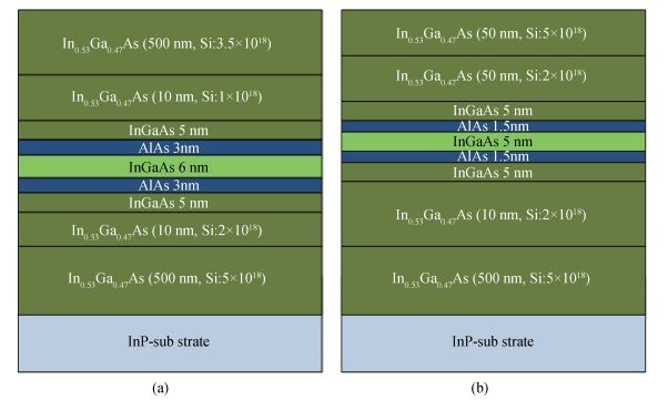
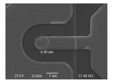
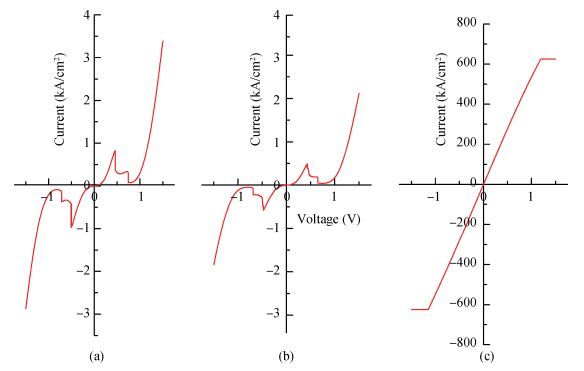
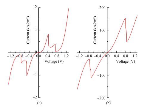
Resonant tunneling diodes (RTD) have the potential for compact and coherent terahertz (THz) sources operating at room temperature, but their low output power severely restricts their application in THz frequency range. In this paper, two methods are adopted to increase the peak current of RTD for enhancing its output power. First, different metal contact systems (including Pt/Ti/Pt/Au and AuGe/Ni/Au) for RTD contact are introduced, and a higher current of RTD with Pt/Ti/Pt/Au contact demonstrates the superior contact characteristic of Pt/Ti/Pt/Au contact system. Second, the double barrier structure (DBS) of RTD is well designed to further improve the characteristic of RTD, and a high peak current of 154 kA/cm2 is achieved at room temperature. The improved peak current is very beneficial for increasing the output power of RTD oscillator.

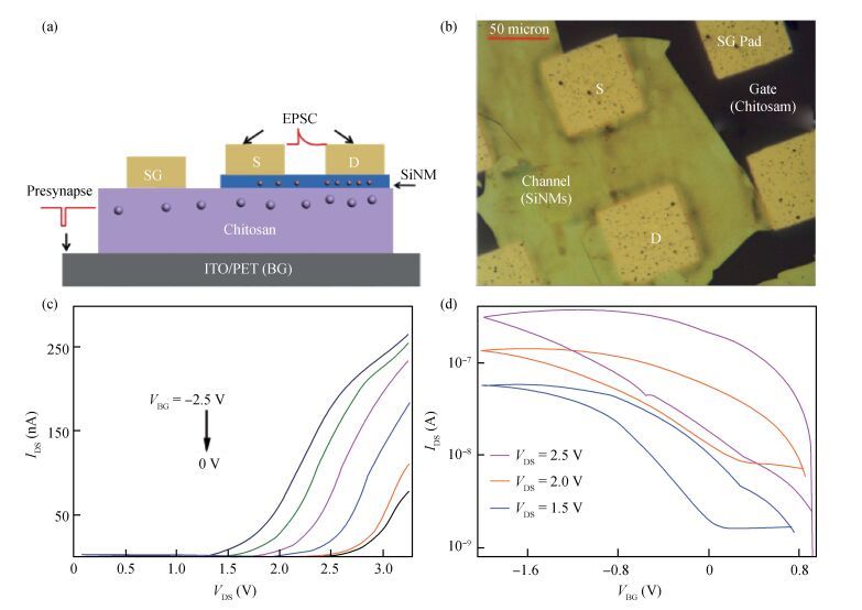
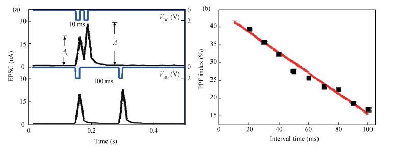
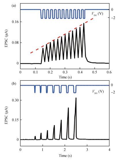
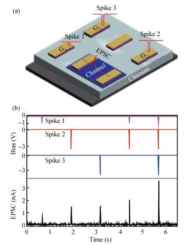
Silicon nanomembrane (SiNM) transistors gated by chitosan membrane were fabricated on plastic substrate to mimic synapse behaviors. The device has both a bottom proton gate (BG) and multiple side gates (SG). Electrical transfer properties of BG show hysteresis curves different from those of typical SiO2 gate dielectric. Synaptic behaviors and functions by linear accumulation and release of protons have been mimicked on this device:excitatory post-synaptic current (EPSC) and paired pulse facilitation behavior of biological synapses were mimicked and the paired-pulse facilitation index could be effectively tuned by the spike interval applied on the BG. Synaptic behaviors and functions, including short-term memory and long-term memory, were also experimentally demonstrated in BG mode. Meanwhile, spiking logic operation and logic modulation were realized in SG mode.

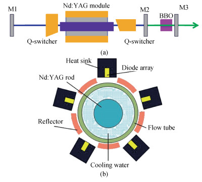
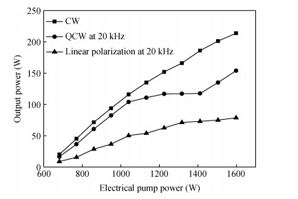
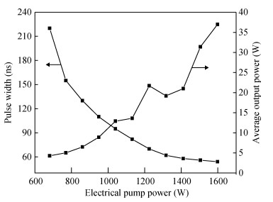
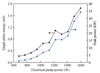
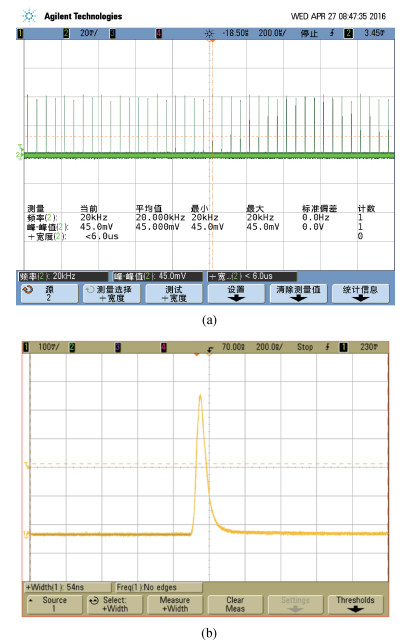
A simple and compact linear resonator green laser at 532 nm is generated by intracavity frequencydoubling of a diode-side-pumped acousto-optically (AO) Q-switched Nd:YAG laser at 1064 nm. Two acoustooptic Q-switches were placed orthogonally with each other to improve the hold-off capacity. As high as 214 W of continuous-wave (CW) and 154 W of quasi-continuous-wave (QCW) output power at 1064 nm were obtained when the pumping power was 1598 W. The type Ⅰ phase-matched BBO crystal was used as the nonlinear medium in the second harmonic generation. A green laser with an average output power of 37 W was obtained at a repetition rate of 20 kHz and a pulse width of 54 ns, which corresponds to pulse energy of 1.85 mJ per pulse and a peak power 34.26 kW, respectively.
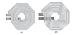
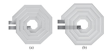
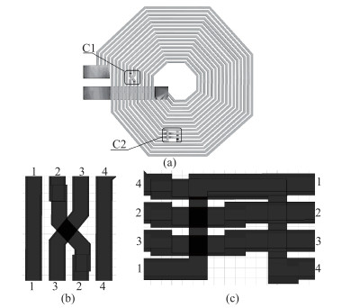
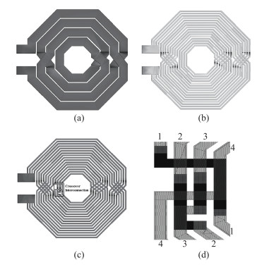
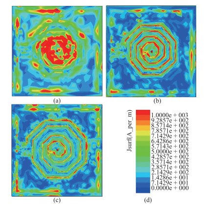
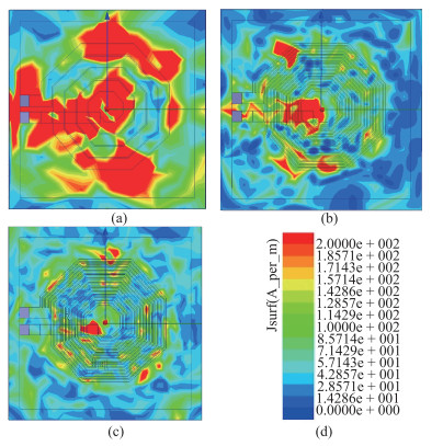
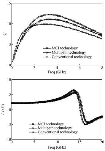
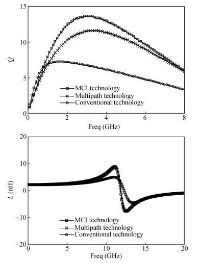
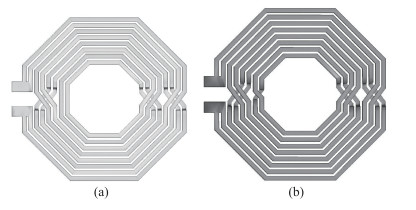
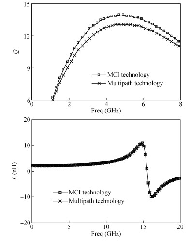
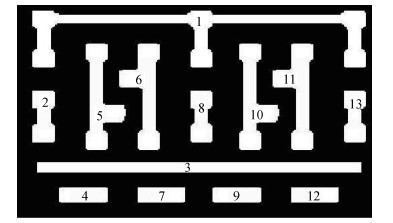
In this paper, the MCI (multipath crossover interconnection) technique for octagon single and symmetrical spiral inductors has been presented to improve the quality factor. The metal wires of the single and symmetrical inductors formed by the top metal are divided into multiple segments according to the depth of the skin effects. The outermost path of the metal is crossover-interconnected to the innermost path by the underlayer metal and via The crossover technique makes the lengths of the total current paths between two ports approximately equal to each other. Therefore, the induced magnetic flux and resistance of each path can be balanced and the Q-factor of spiral inductors can be enhanced. The proposed MCI technique has been validated by the electromagnetic simulation with the 130-nm 1P6M SiGe BiCMOS process. For the devices with occupying areas of 240×240μm2, results of electromagnetic simulation show that about 24% improvement in the Q-peak (3.3 GHz) of the MCI single inductor as compared to conventional single inductors (3.1 GHz), and about 88.1% improvement in the Q-peak (3.2 GHz) of the MCI symmetrical inductor as compared to conventional symmetrical inductors (1.8 GHz).

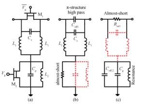
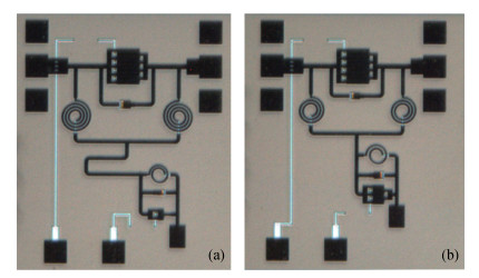
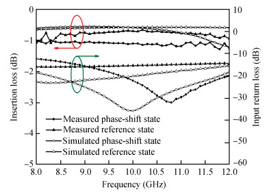
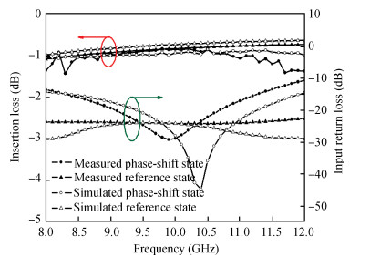
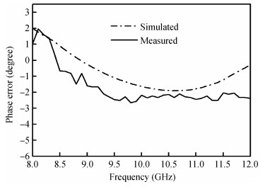
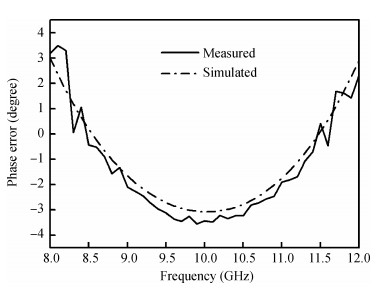
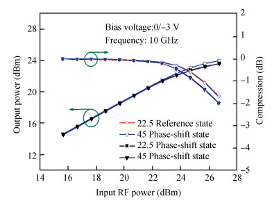
The design approach and performance of a 22.5°/45°digital phase shifter based on a switched filter network for X-band phased arrays are described. Both the MMIC phase shifters are fabricated employing a 0.25μm gate GaAs pHEMT process and share in the same chip size of 0.82×1.06 mm2. The measurement results of the proposed phase shifters over the whole operating frequency range show that the phase shift error is less than 22.5°±2.5°, 45°±3.5°, which shows an excellent agreement with the simulated performance, the insertion loss is within the range of 0.9-1.2 dB for the 22.5°phase shifter and 0.9-1.4 dB for the 45°phase shifter, and the input/output return loss is better than -12.5 and -11 dB respectively. They also achieve the similar P1dB continuous wave power handing capability of 24.8 dBm at 10 GHz. The phase shifters show a good phase shift error, insertion loss and return loss in the X-band (40%), which can be employed into the wide bandwidth multi-bit digital phase shifter.


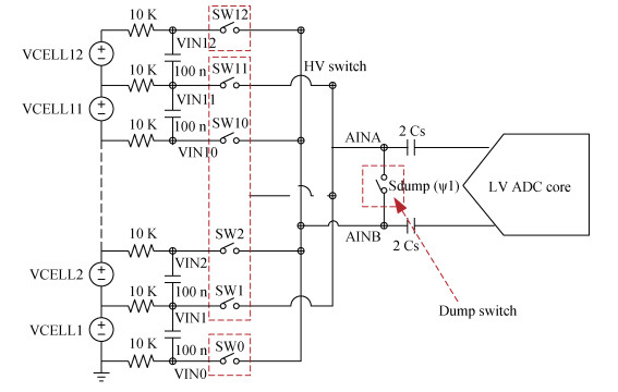
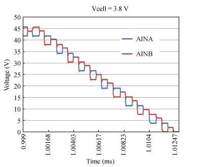
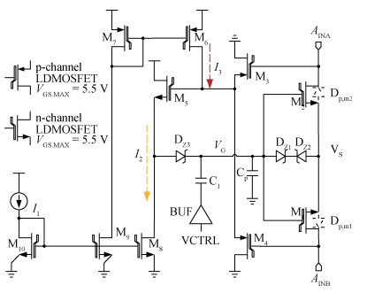
For stacked battery monitoring IC high speed and high precision voltage acquisition requirements, this paper introduces a kind of symmetrical type high voltage switch circuit. This kind of switch circuit uses the voltage following structure, which eliminates the leakage path of input signals. At the same time, this circuit adopts a high speed charge pump structure, in any case the input signal voltage is higher than the supply voltage, it can fast and accurately turn on high voltage MOS devices, and convert the battery voltage to an analog to digital converter. The proposed high voltage full symmetry switch has been implemented in a 0.18μm BCD process; simulated and measured results show that the proposed switch can always work properly regardless of the polarity of the voltage difference between the input signal ports and an input signal higher than the power supply.


As the technology scales advancing into the nanometer region, the concept of yield has become an increasingly important design metric. To reduce the yield loss caused by local defects, layout optimization can play a critical role. In this paper, we propose a new open sensitivity-based model with consideration of the blank space around the net, and study the corresponding net optimization. The proposed new model not only has a high practicability in the selection of nets to be optimized but also solves the issue of the increase in short critical area brought during the open optimization, which means to reduce the open critical area with no new short critical area produced, and thereby this model can ensure the decrease of total critical area and finally achieves an integrative optimization. Compared with the models available, the experimental results show that our sensitivity model not only consumes less time with concise algorithm but also can deal with irregular layout, which is out of the scope of other models. At the end of this paper, the effectiveness of the new model is verified by the experiment on the randomly selected five metal layers from the synthesized OpenSparc circuit layout.


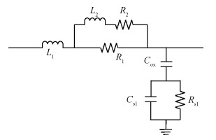
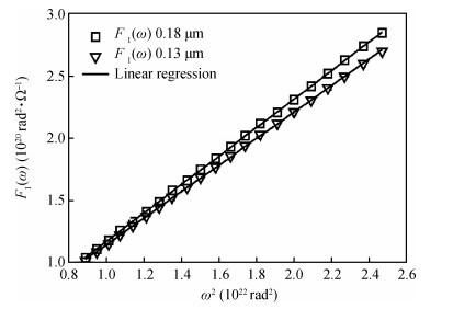
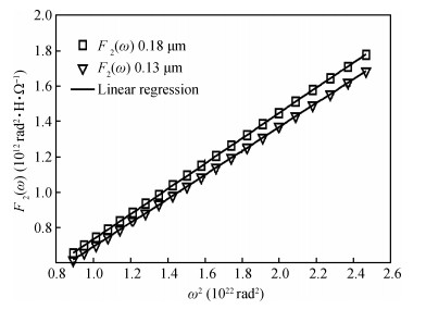
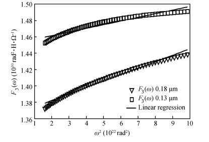
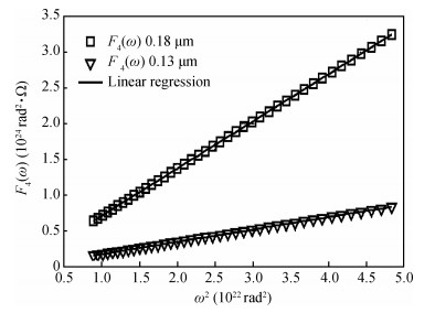
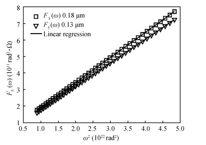
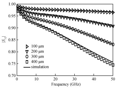
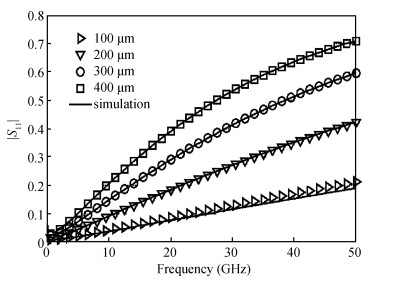
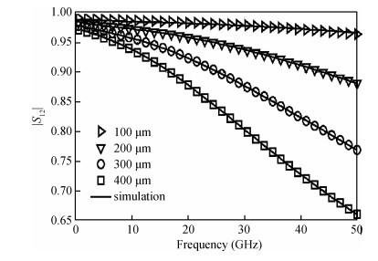
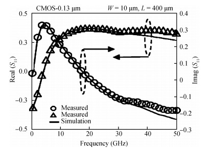
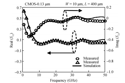
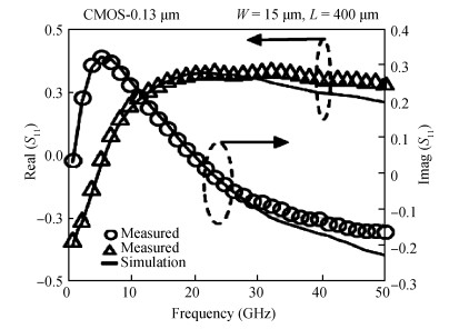
A scalable wideband equivalent circuit model of silicon-based on-chip transmission lines is presented in this paper along with an efficient analytical parameter extraction method based on improved characteristic function approach, including a relevant equation to reduce the deviation caused by approximation. The model consists of both series and shunt lumped elements and accounts for high-order parasitic effects. The equivalent circuit model is derived and verified to recover the frequency-dependent parameters at a range from direct current to 50 GHz accurately. The scalability of the model is proved by comparing simulated and measured scattering parameters with the method of cascade, attaining excellent results based on samples made from CMOS 0.13 and 0.18μm process.