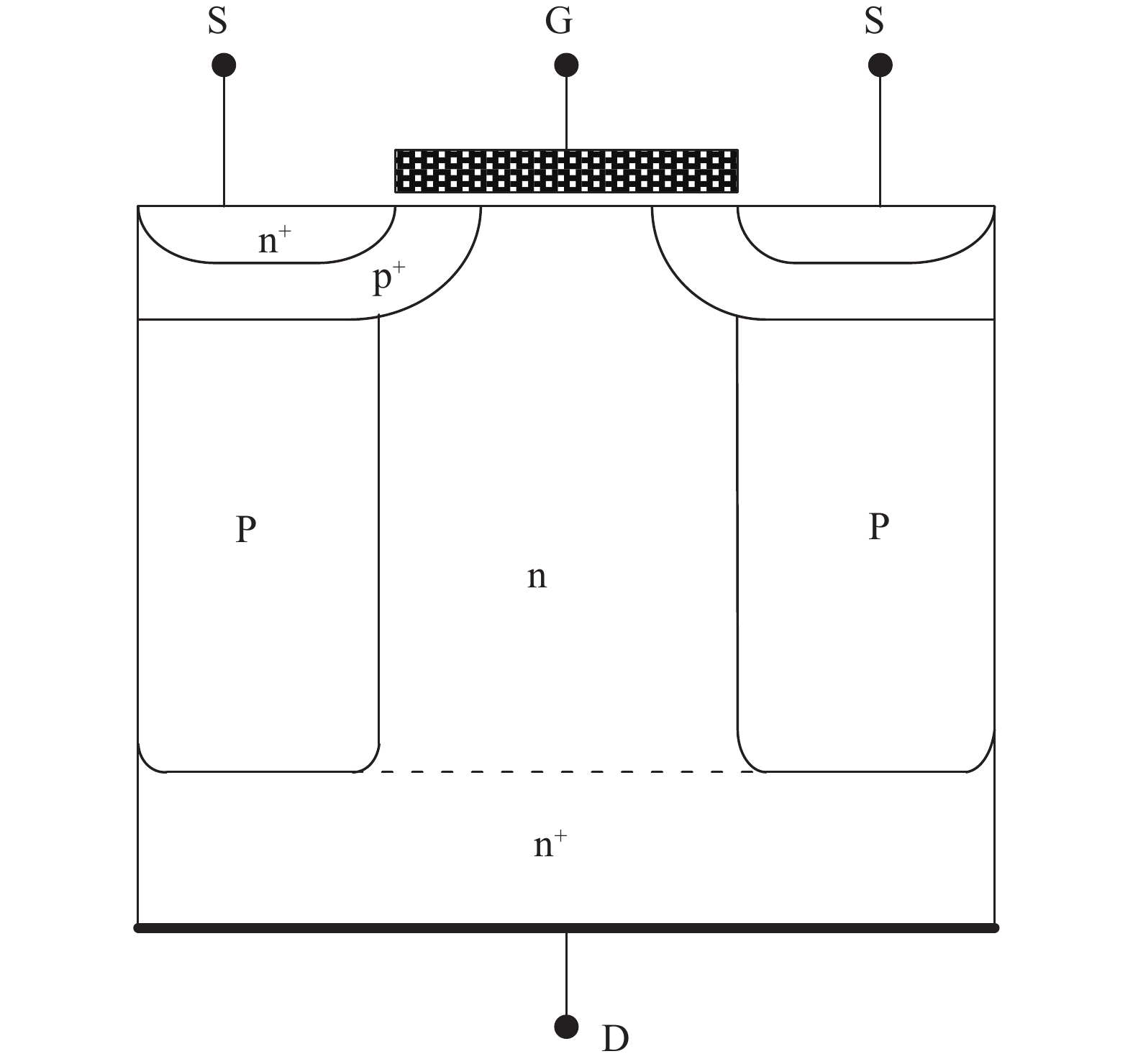
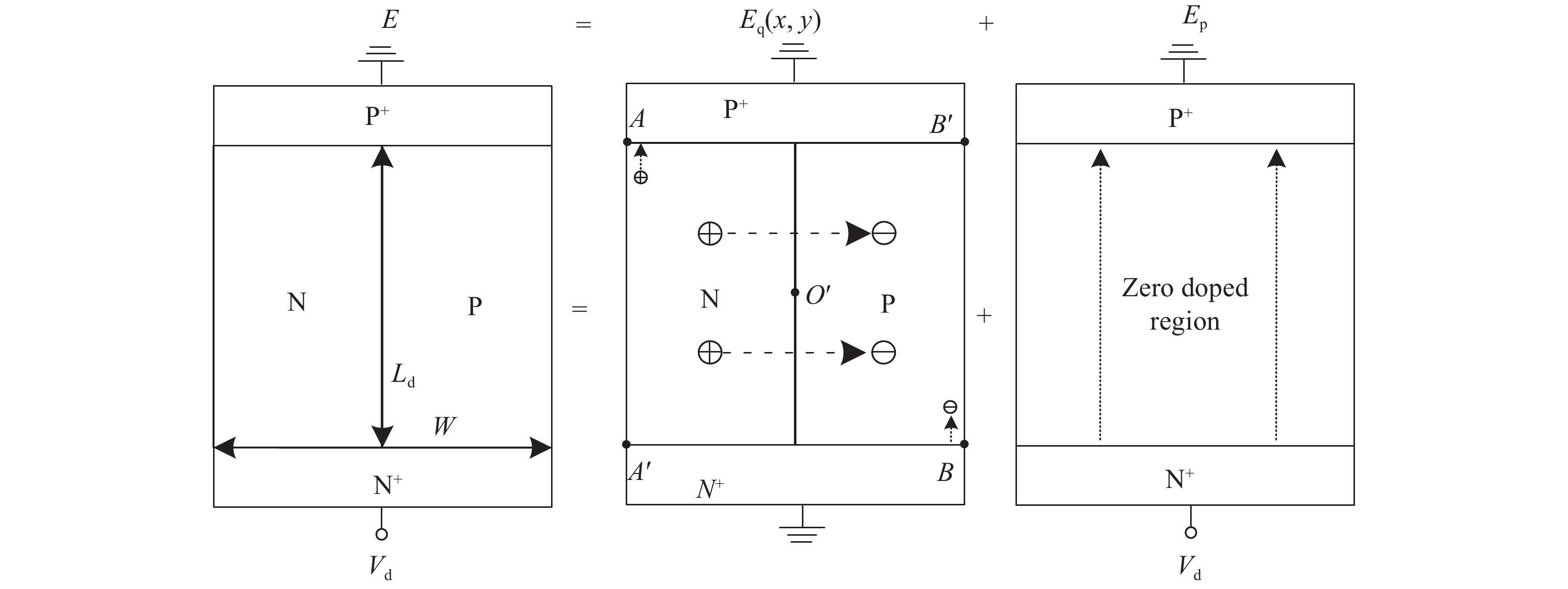
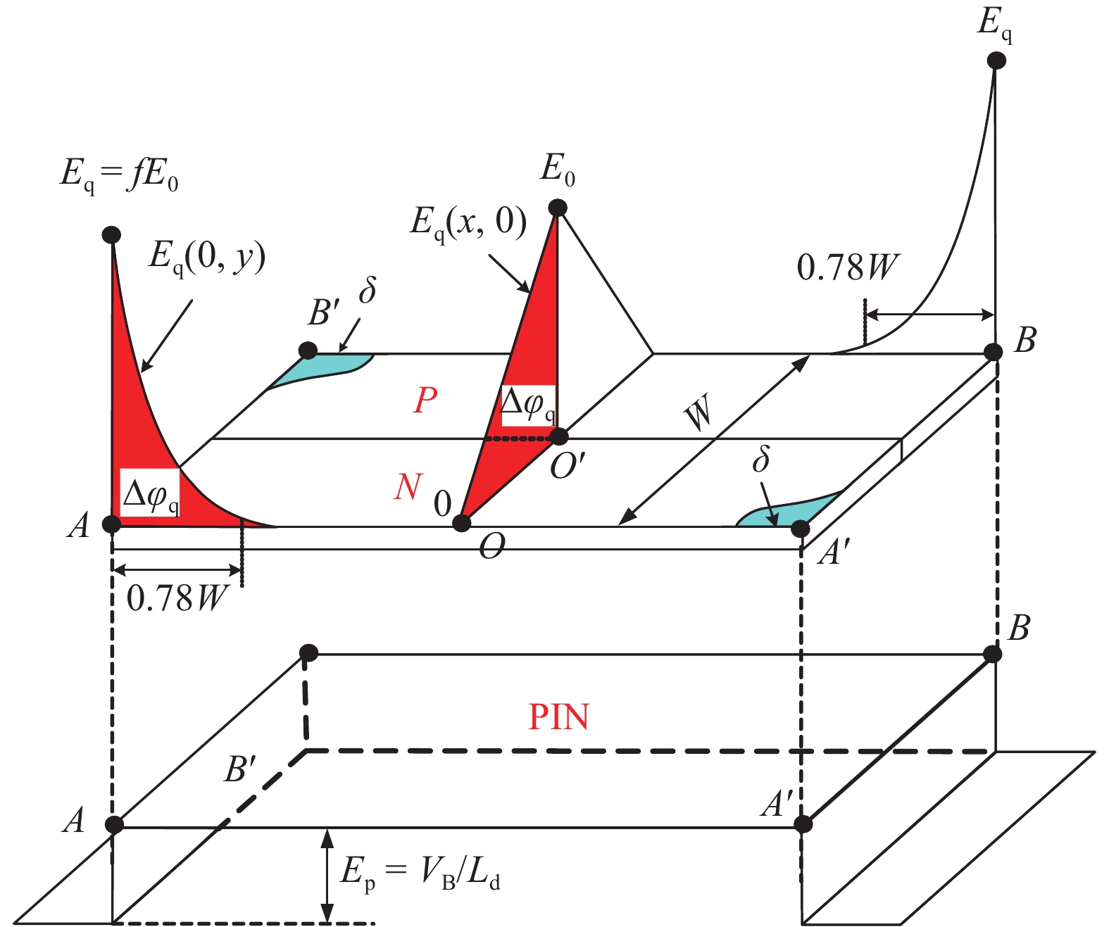
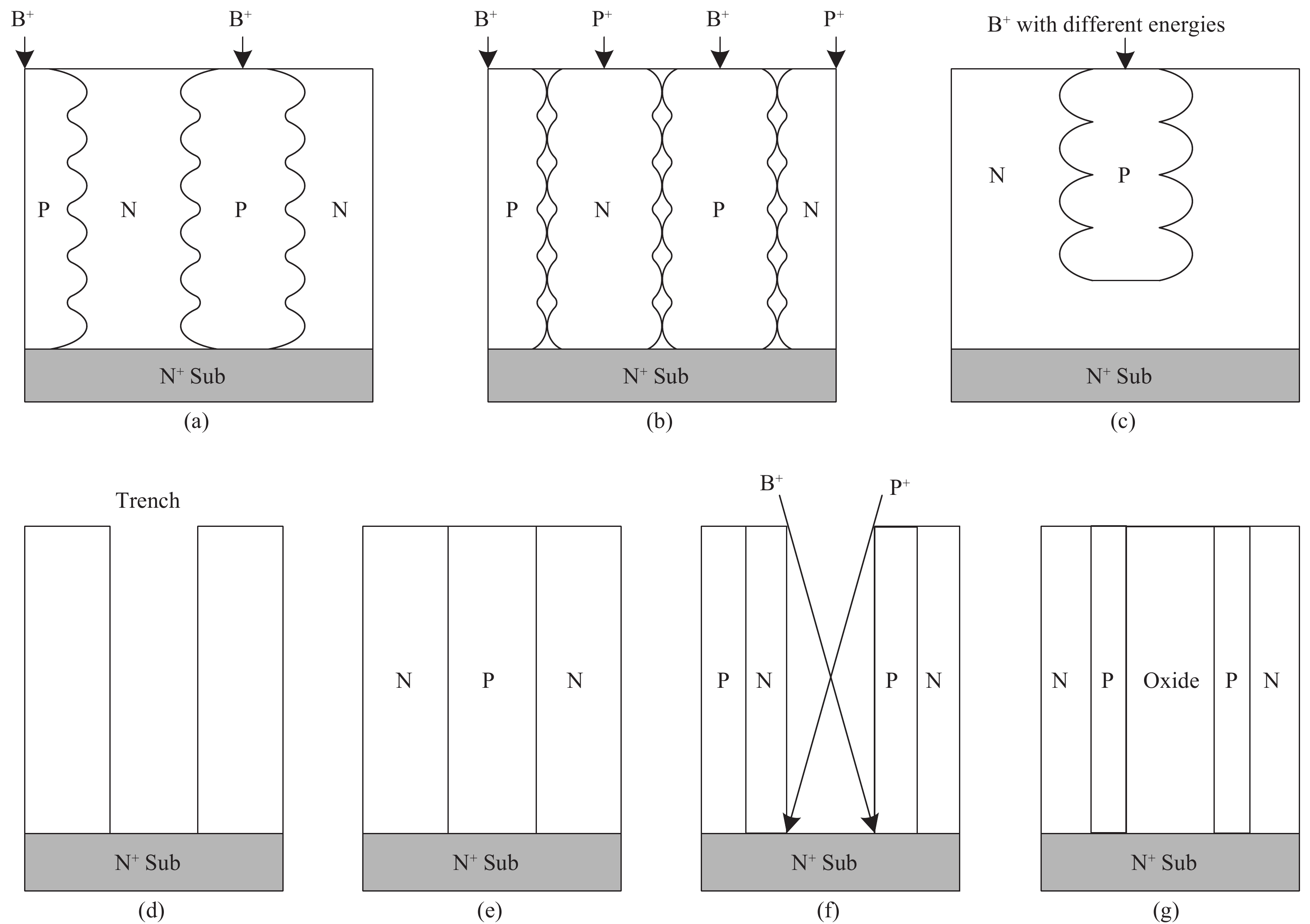
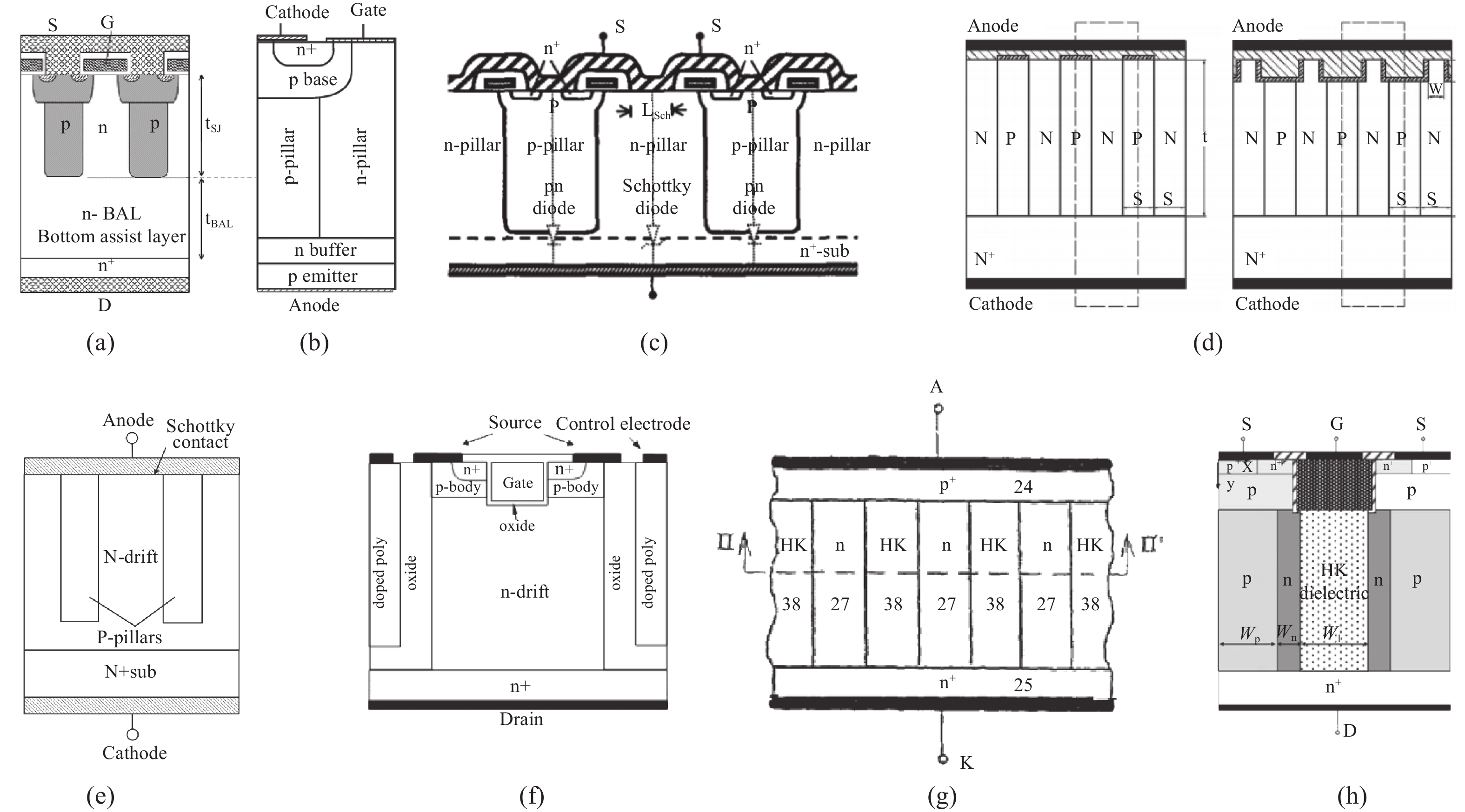
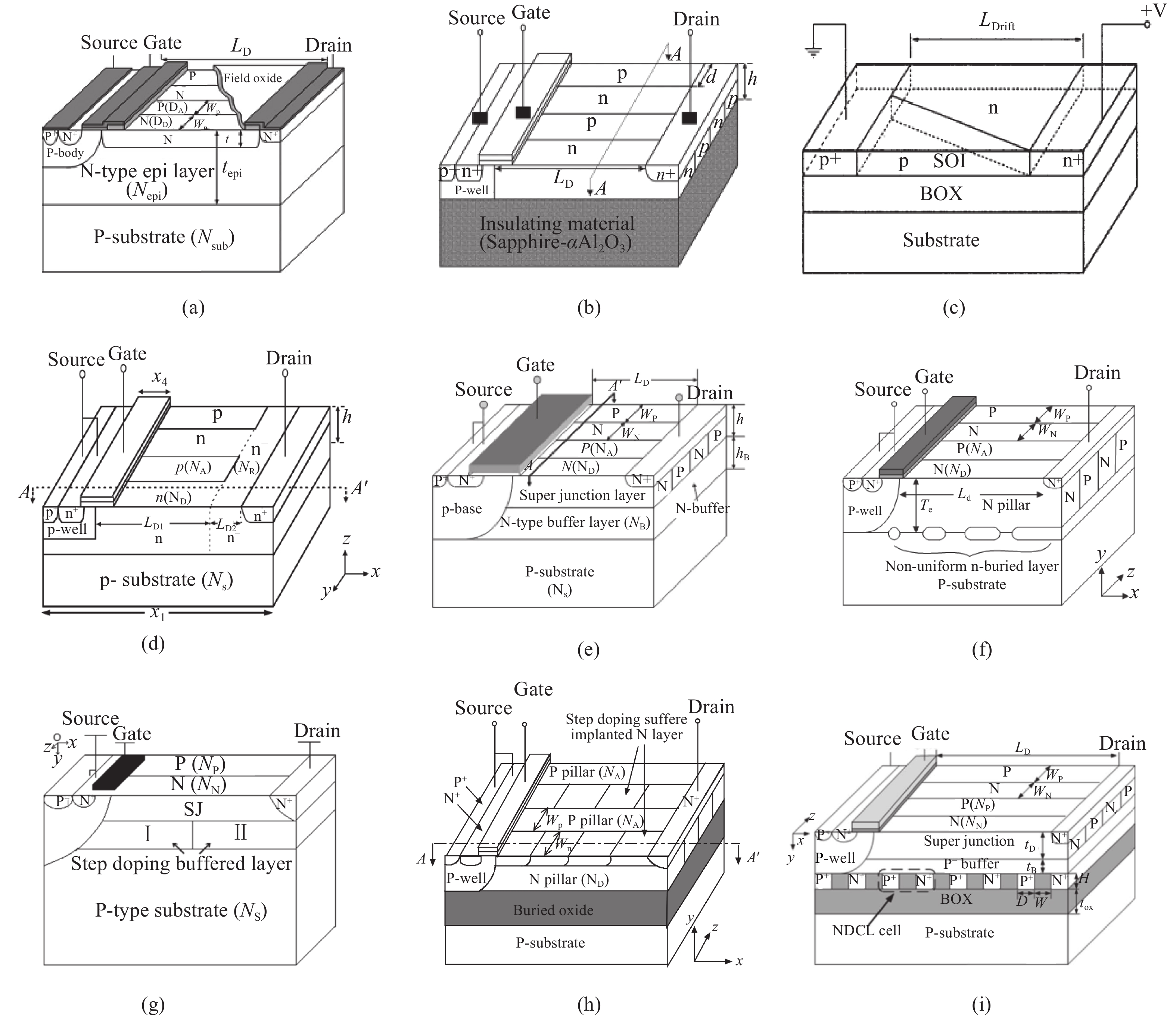
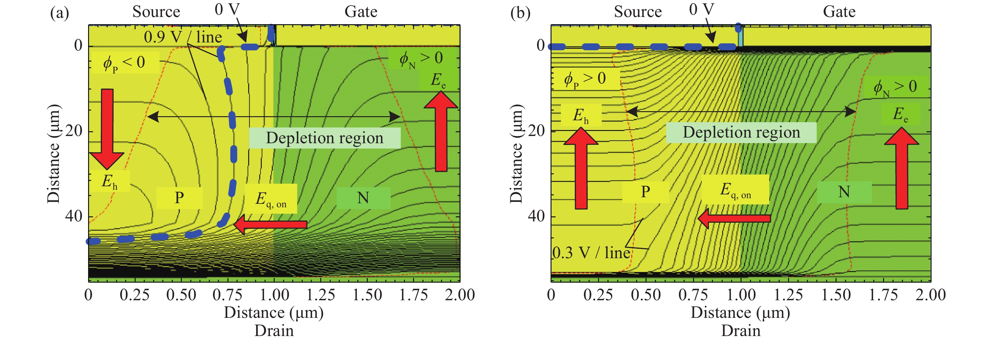
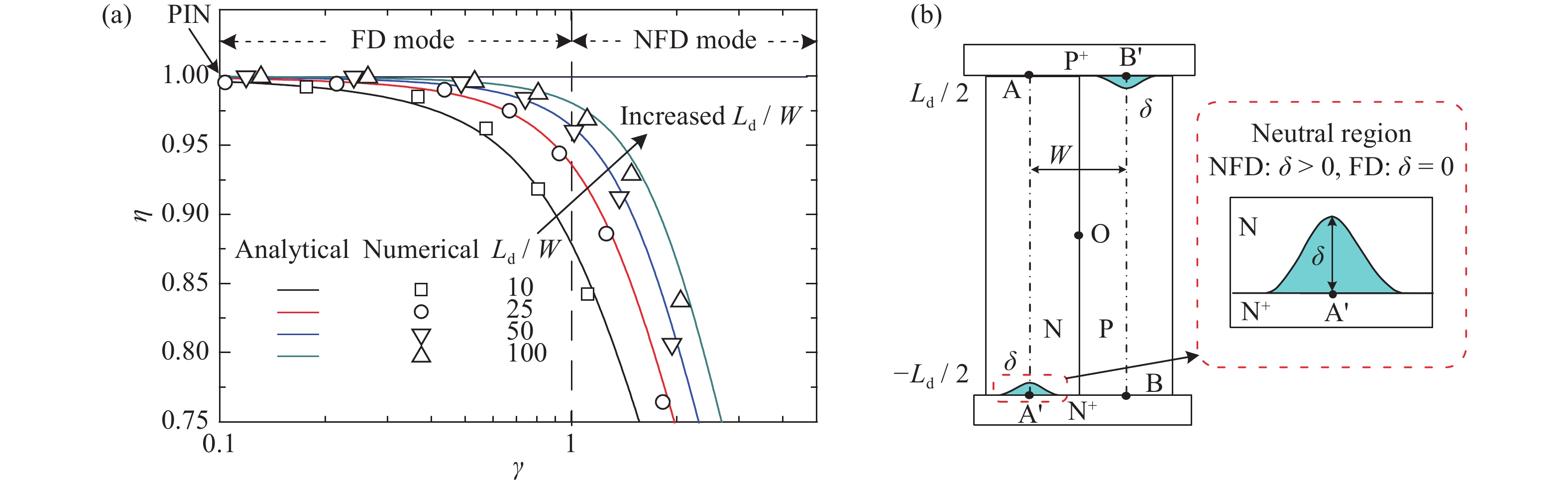
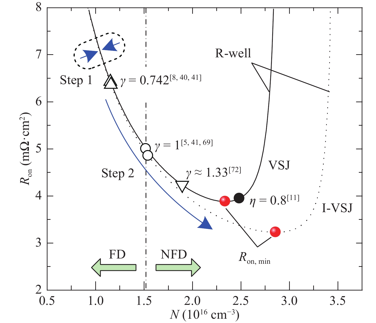
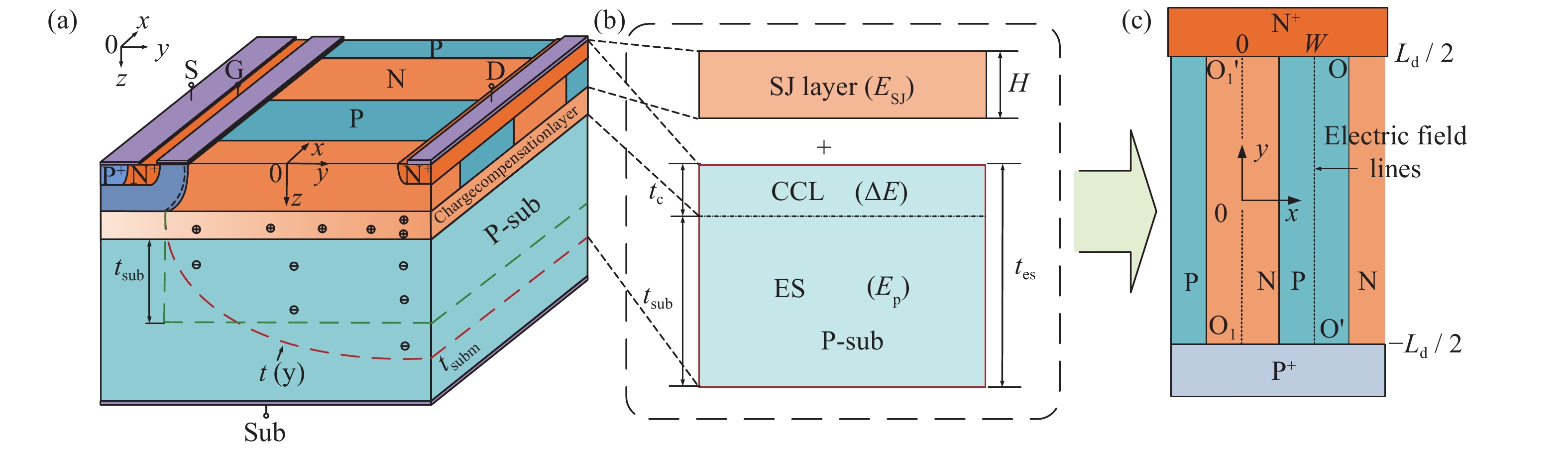
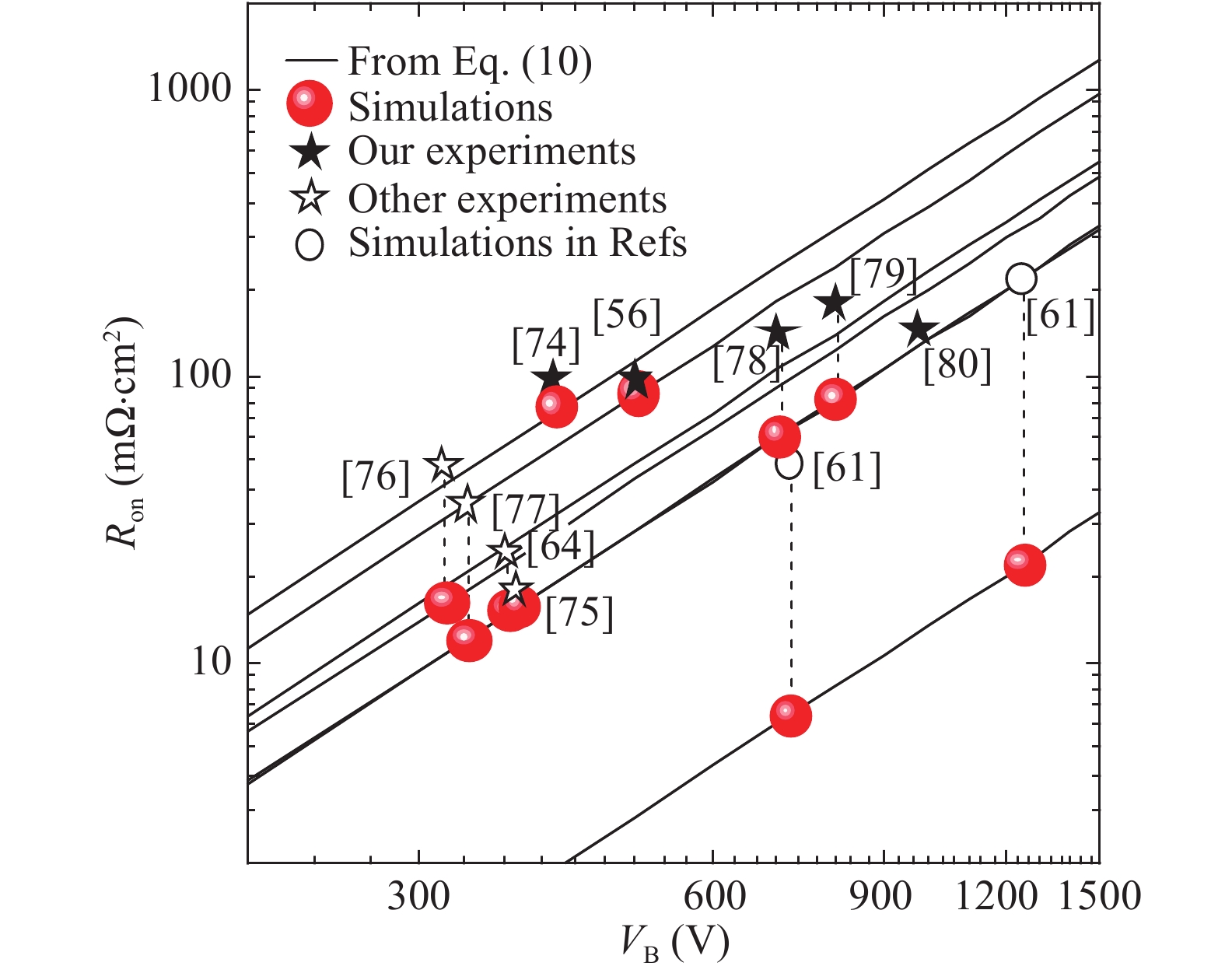
The super junction (SJ) has been recognized as the " milestone” of the power MOSFET, which is the most important innovation concept of the voltage-sustaining layer (VSL). The basic structure of the SJ is a typical junction-type VSL (J-VSL) with the periodic N and P regions. However, the conventional VSL is a typical resistance-type VSL (R-VSL) with only an N or P region. It is a qualitative change of the VSL from the R-VSL to the J-VSL, introducing the bulk depletion to increase the doping concentration and optimize the bulk electric field of the SJ. This paper firstly summarizes the development of the SJ, and then the optimization theory of the SJ is discussed for both the vertical and the lateral devices, including the non-full depletion mode, the minimum specific on-resistance optimization method and the equivalent substrate model. The SJ concept breaks the conventional " silicon limit” relationship of Ron∝VB2.5, showing a quasi-linear relationship of Ron∝VB1.03.


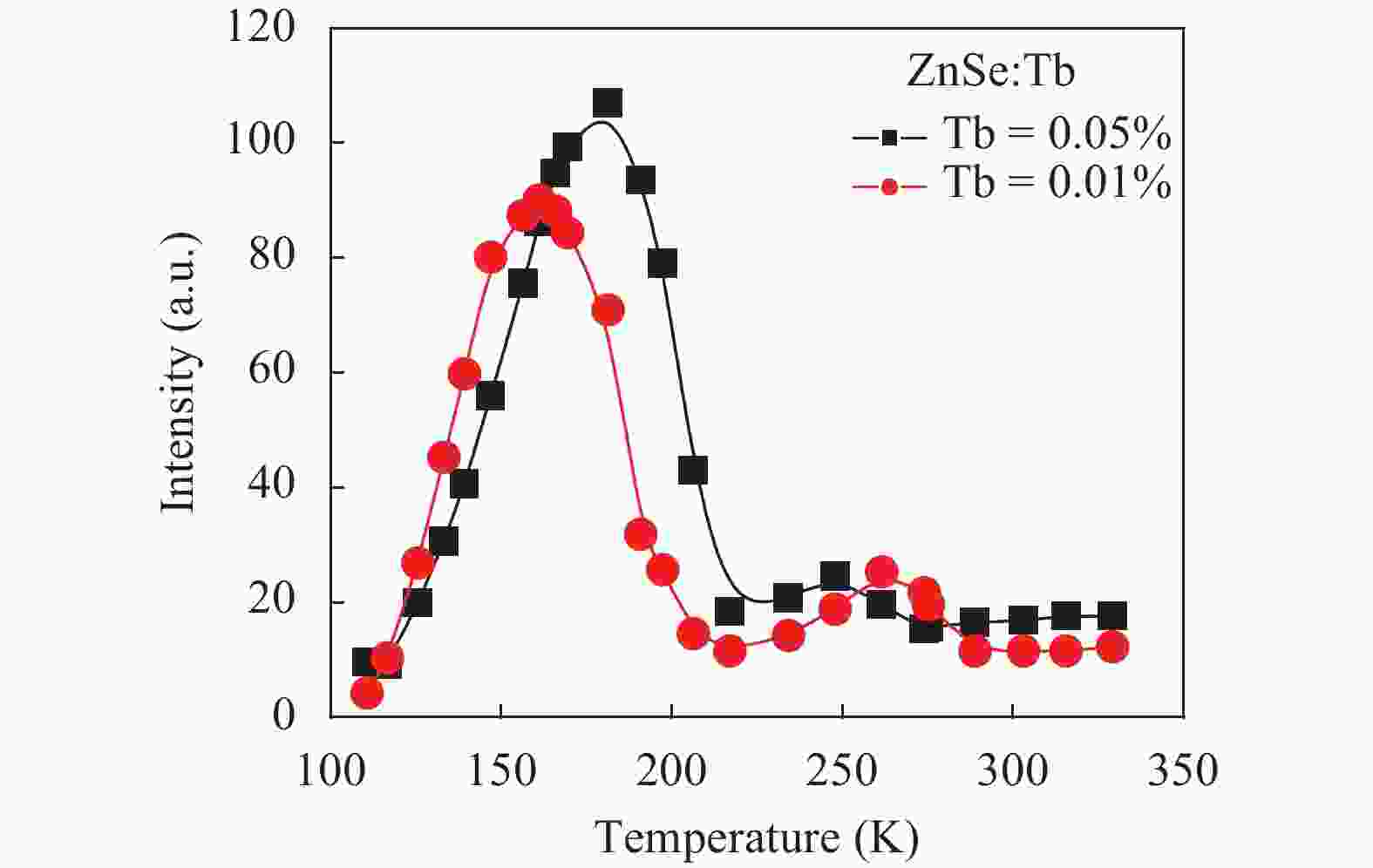
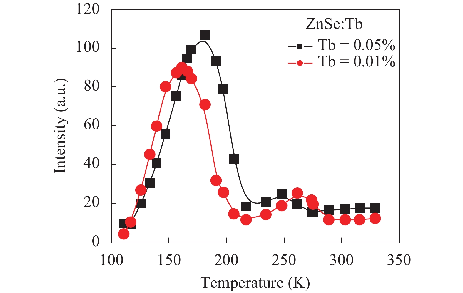
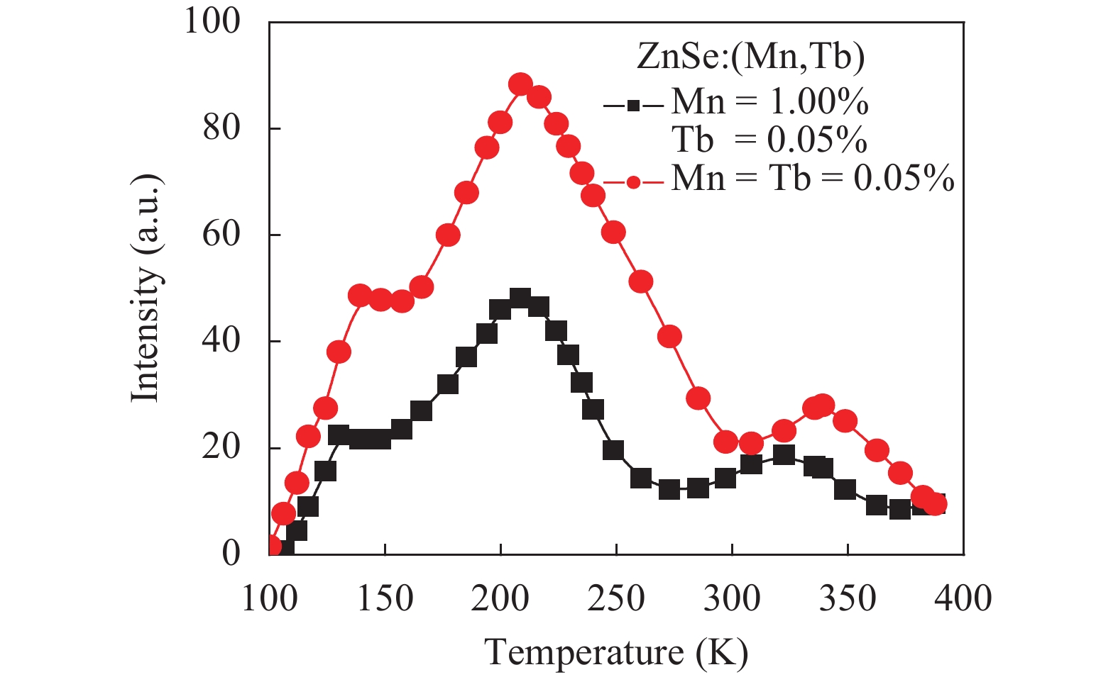
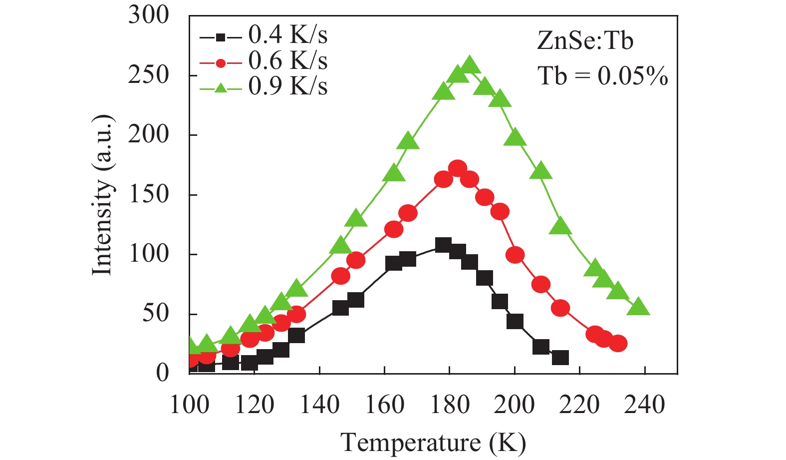
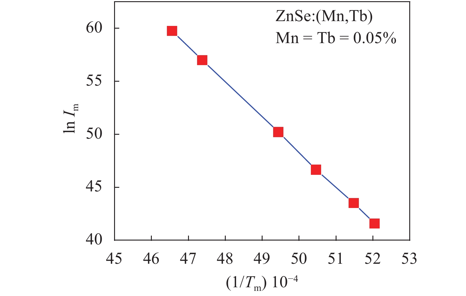
Thermoluminescence studies were performed of ZnSe:Tb and ZnSe:(Mn, Tb) phosphors. A method of preparation for ZnSe phosphors doped with Tb and (Mn, Tb) has been discussed. The thermoluminescence (TL) properties of these phosphors have been studied from 100 to 370 K temperature after exciting by UV radiation (365 nm) at three uniform heating rates 0.4, 0.6 and 0.9 K/s. The trapping parameters like trap depth, lifetime of electrons and capture cross-section have also been determined using various methods.


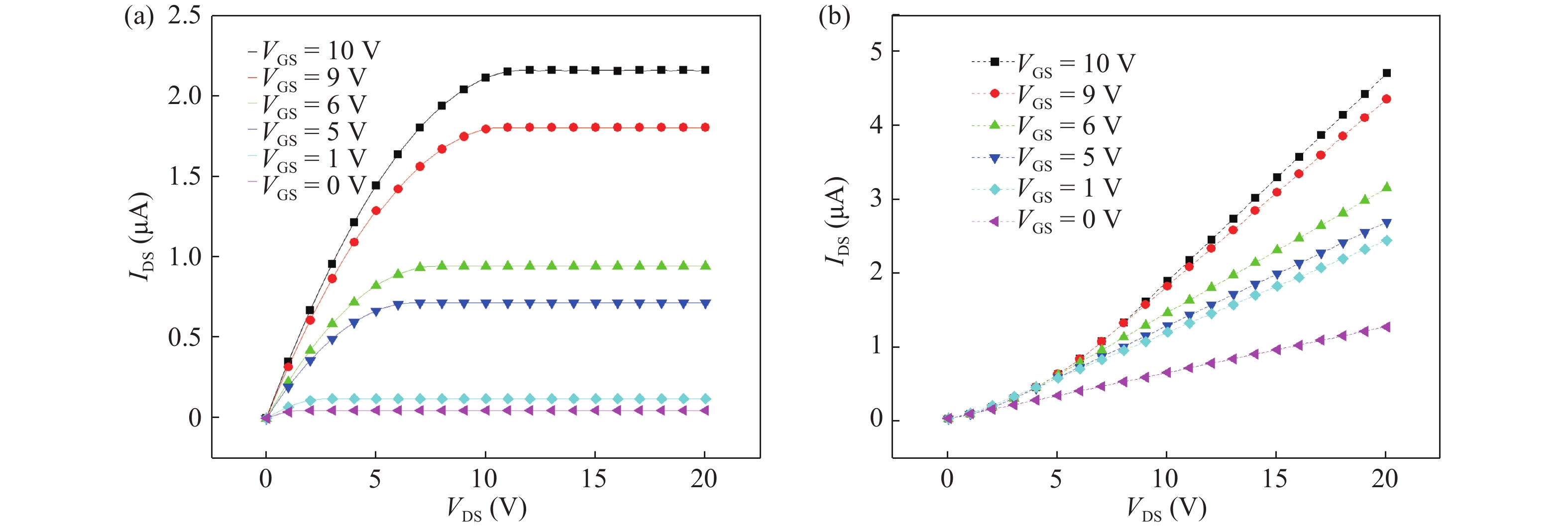
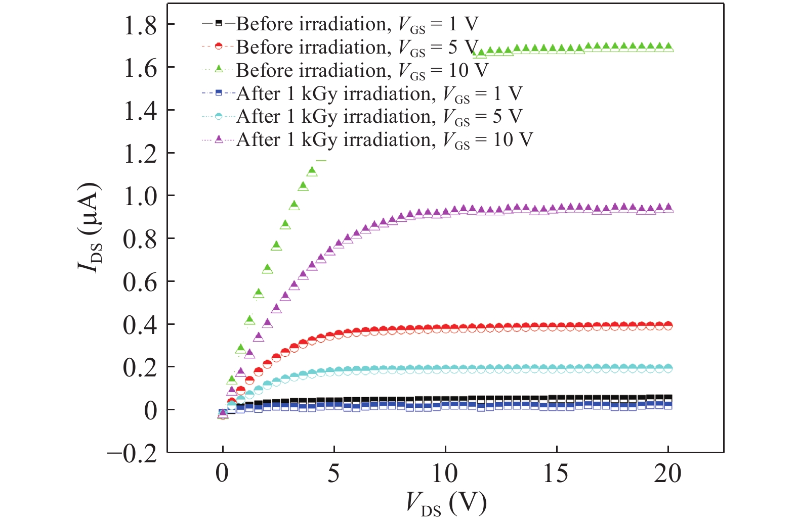
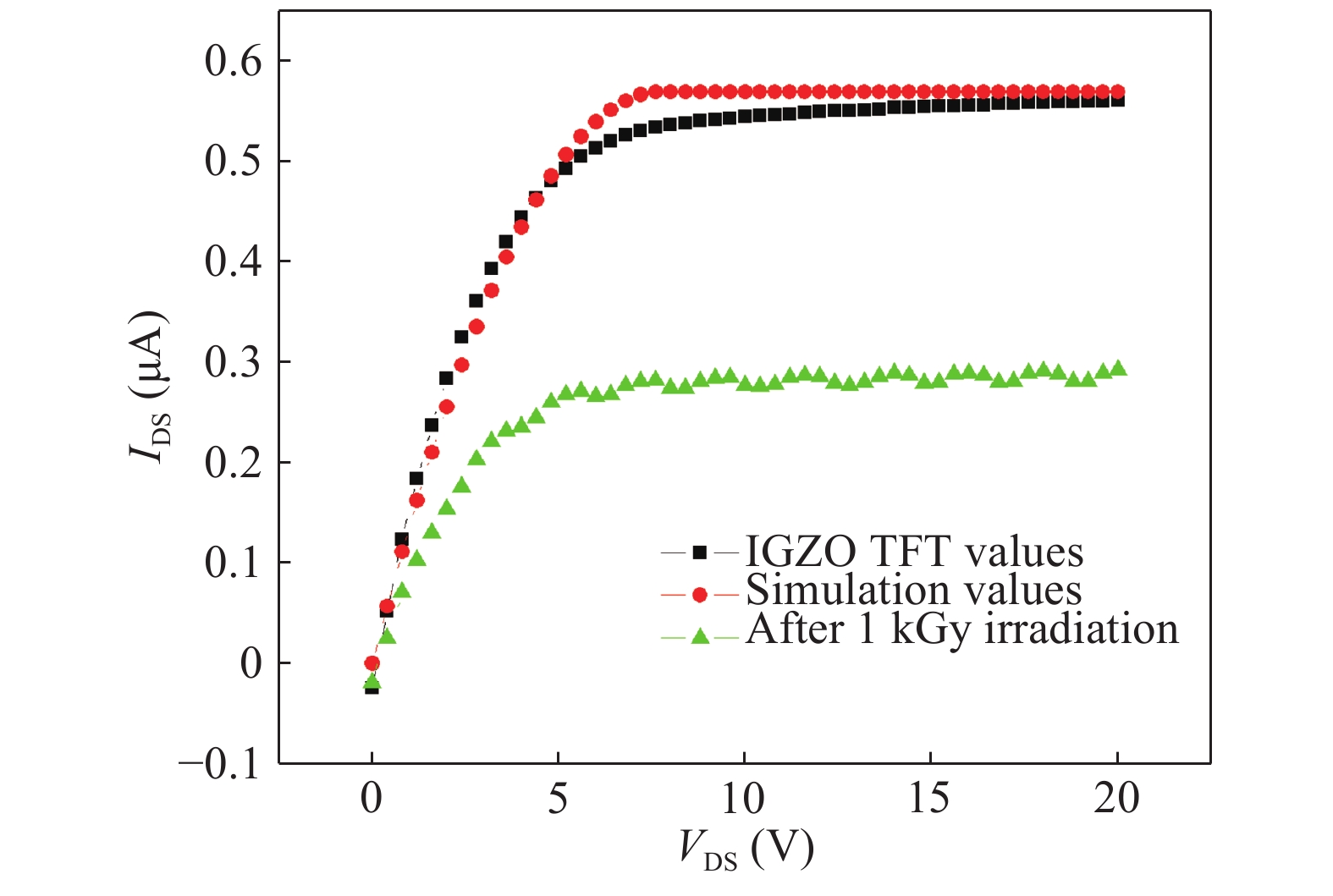
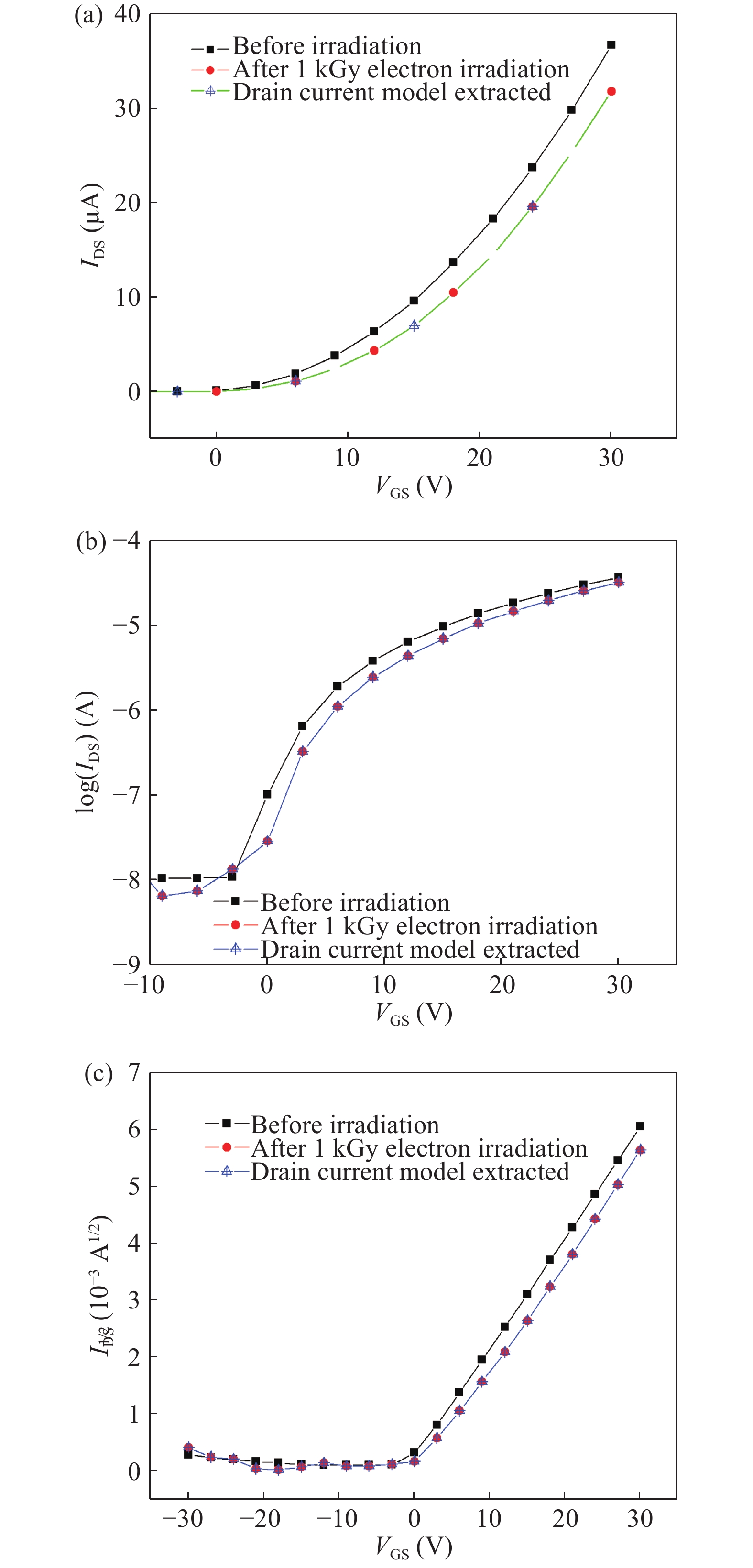
An efficient drain current simulation model for the electron irradiation effect on the electrical parameters of amorphous In–Ga–Zn–O (IGZO) thin-film transistors is developed. The model is developed based on the specifications such as gate capacitance, channel length, channel width, flat band voltage etc. Electrical parameters of un-irradiated IGZO samples were simulated and compared with the experimental parameters and 1 kGy electron irradiated parameters. The effect of electron irradiation on the IGZO sample was analysed by developing a mathematical model.


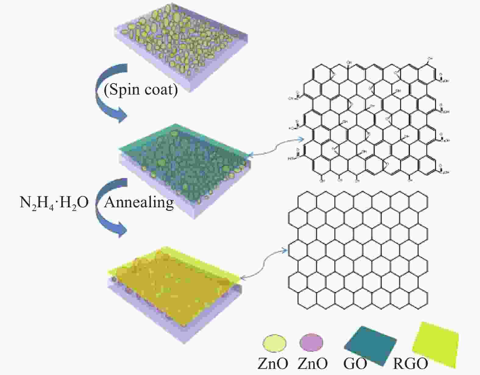
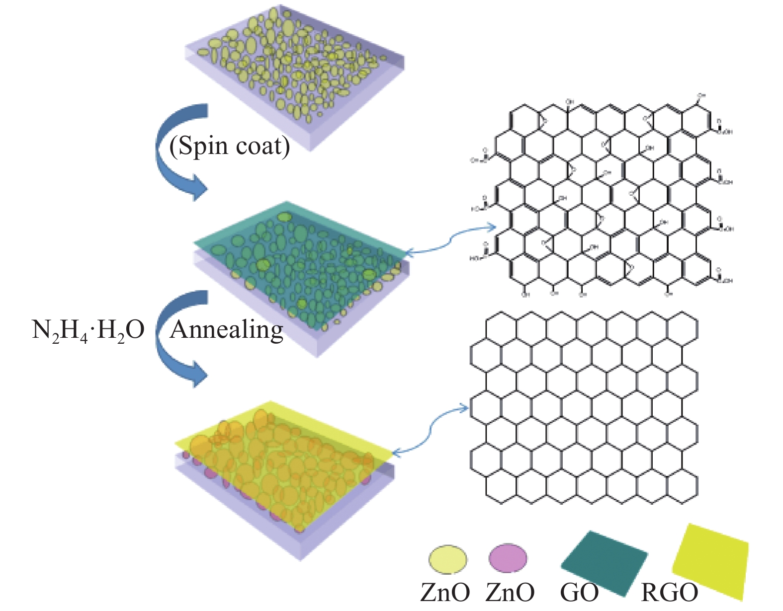
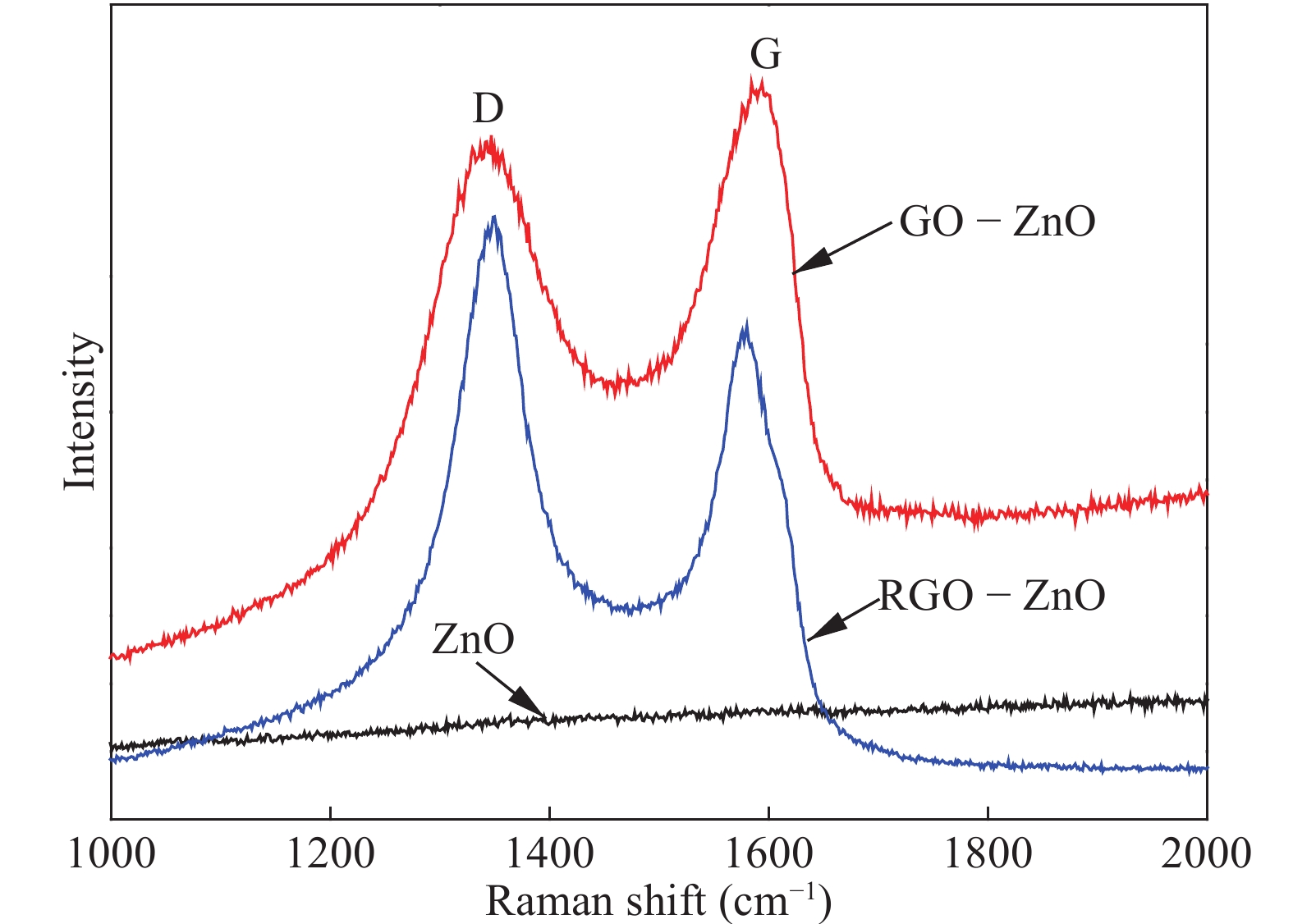
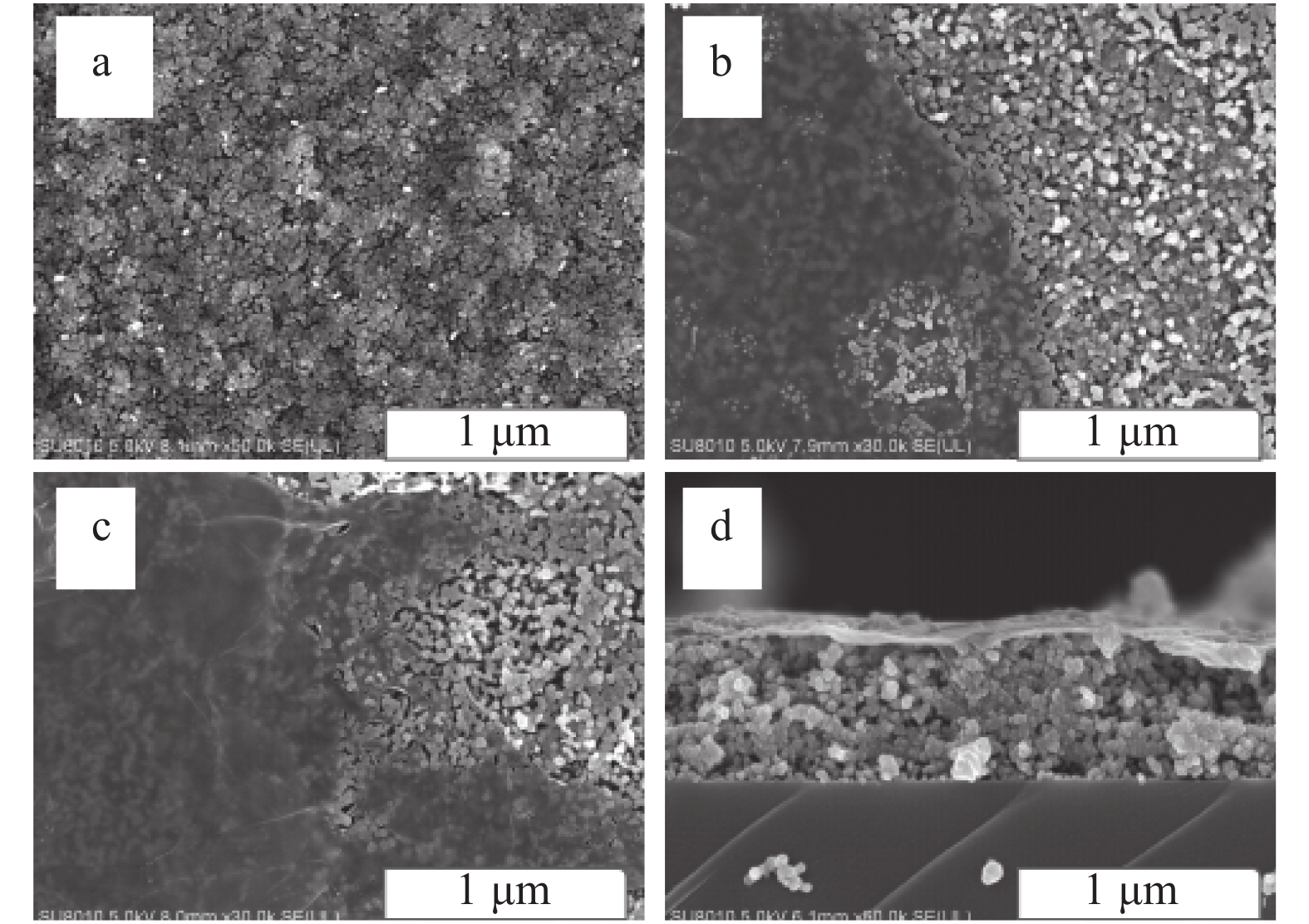
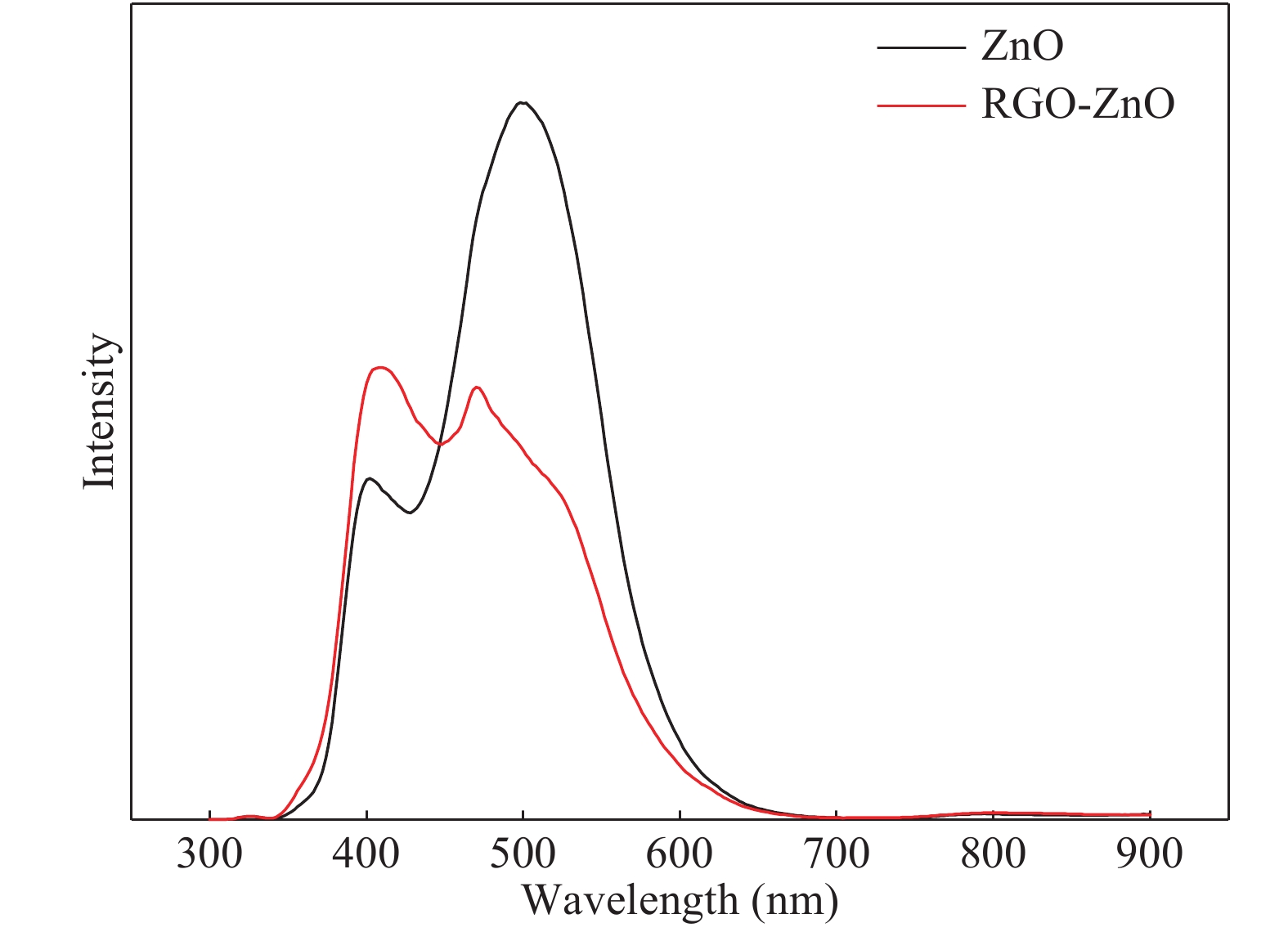
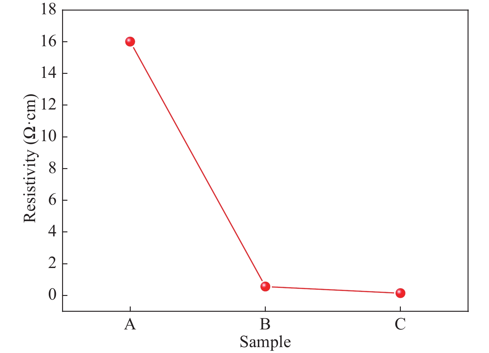
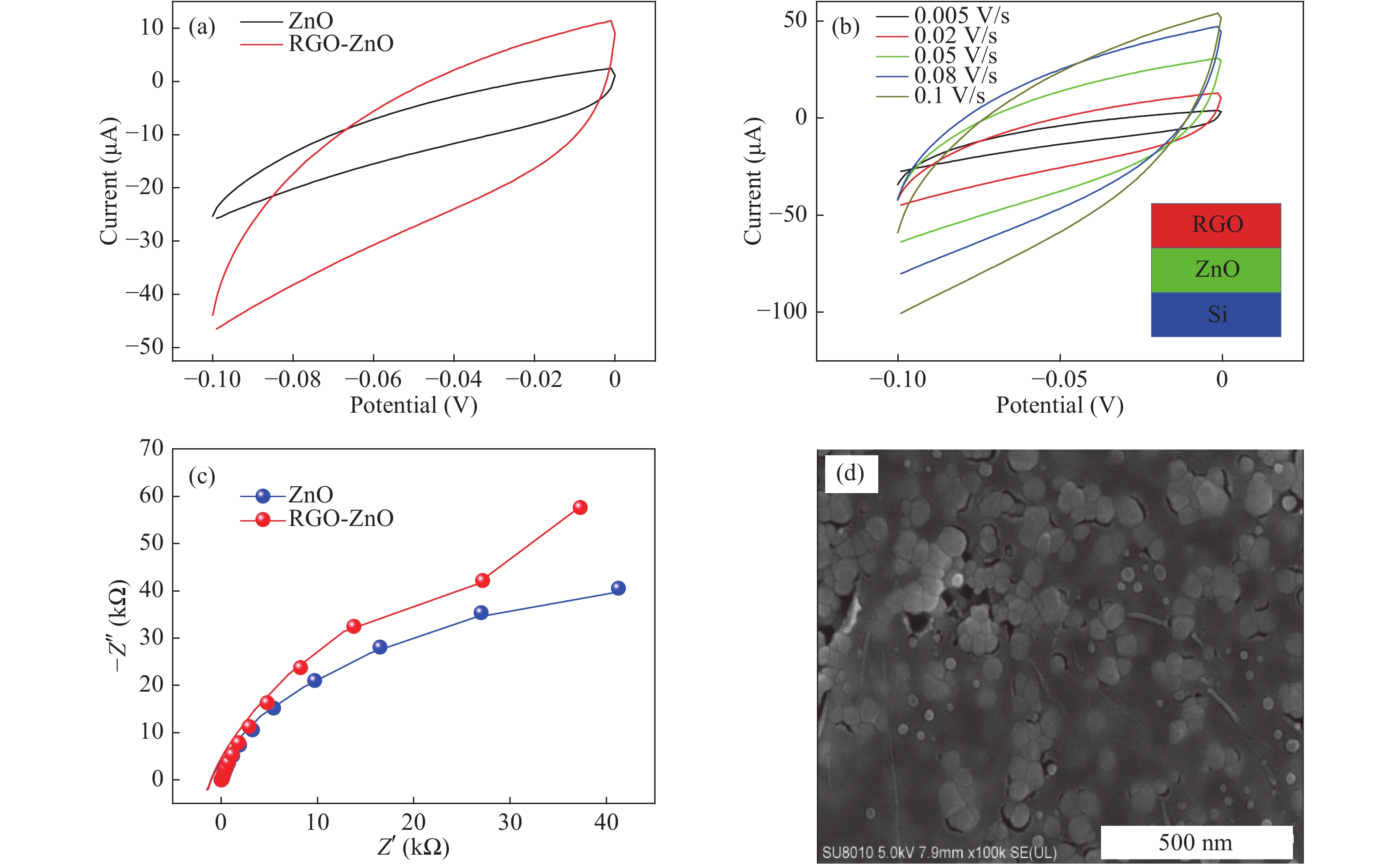
ZnO films coated with reduced graphene oxide (RGO-ZnO) were prepared by a simple chemical approach. The graphene oxide (GO) films transferred onto ZnO films by spin coating were reduced to RGO films by two steps (exposed to hydrazine vapor for 12 h and annealed at 600 °C). The crystal structures, electrical and photoluminescence properties of RGO-ZnO films on quartz substrates were systematically studied. The SEM images illustrated that RGO layers have successfully been coated on the ZnO films very tightly. The PL properties of RGO-ZnO were studied. PL spectra show two sharp peaks at 390 nm and a broad visible emission around 490 nm. The resistivity of RGO-ZnO films was measured by a Hall measurement system, RGO as nanofiller considerably decrease the resistivity of ZnO films. An electrode was fabricated, using RGO-ZnO films deposited on Si substrate as active materials, for super capacitor application. By comparison of different results, we conclude that the RGO-ZnO composite material couples possess the properties of super capacitor.

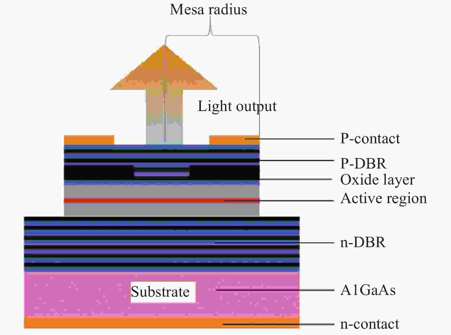
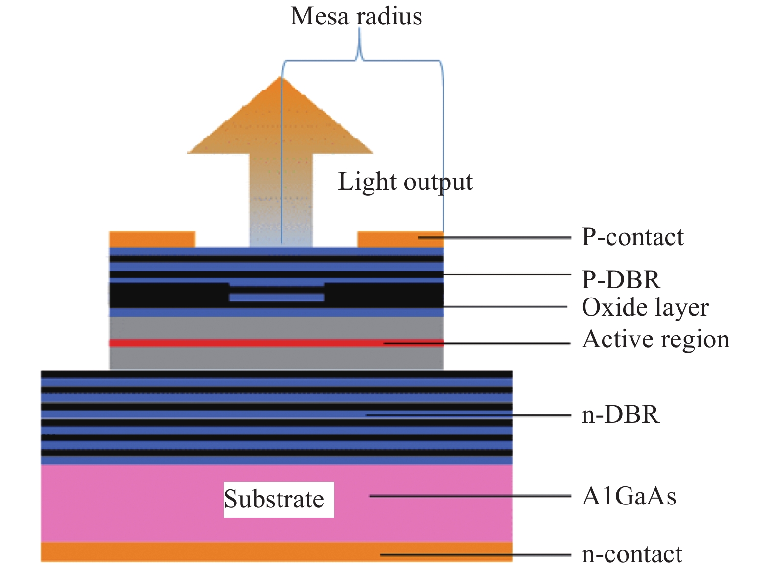
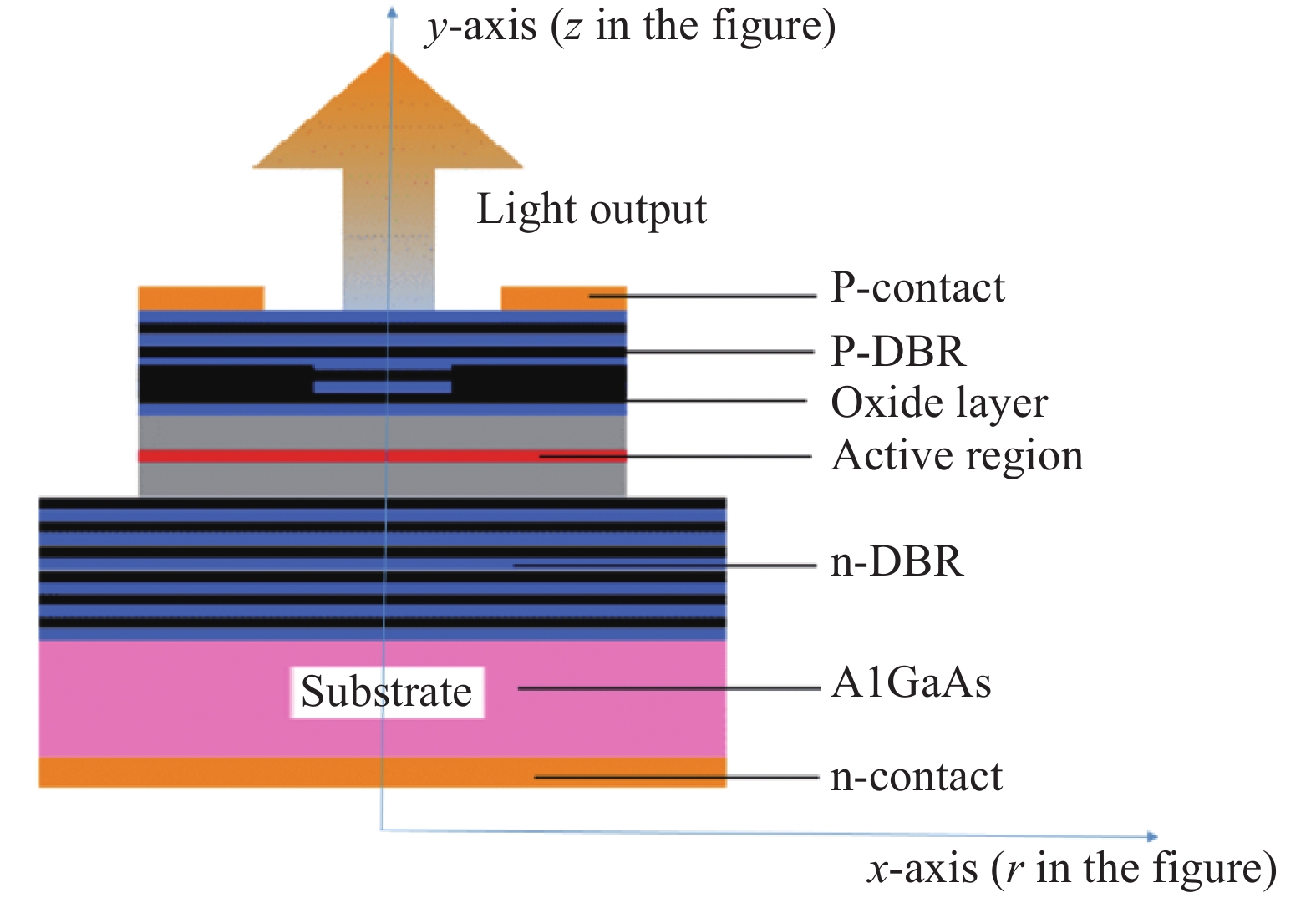
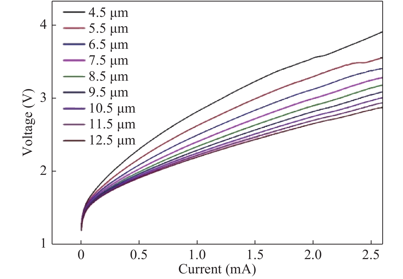
In order to design a single mode 980 nm vertical cavity surface emitting laser (VCSEL), a 2 μm output aperture is designed to guarantee the single mode output. The effects of different mesa sizes on the lattice temperature, the output power and the voltage are simulated under the condition of continuous working at room temperature, to obtain the optimum process parameters of mesa. It is obtained by results of the crosslight simulation software that the sizes of mesa radius are between 9.5 to 12.5 μm, which cannot only obtain the maximum output power, but also improve the heat dissipation of the device.


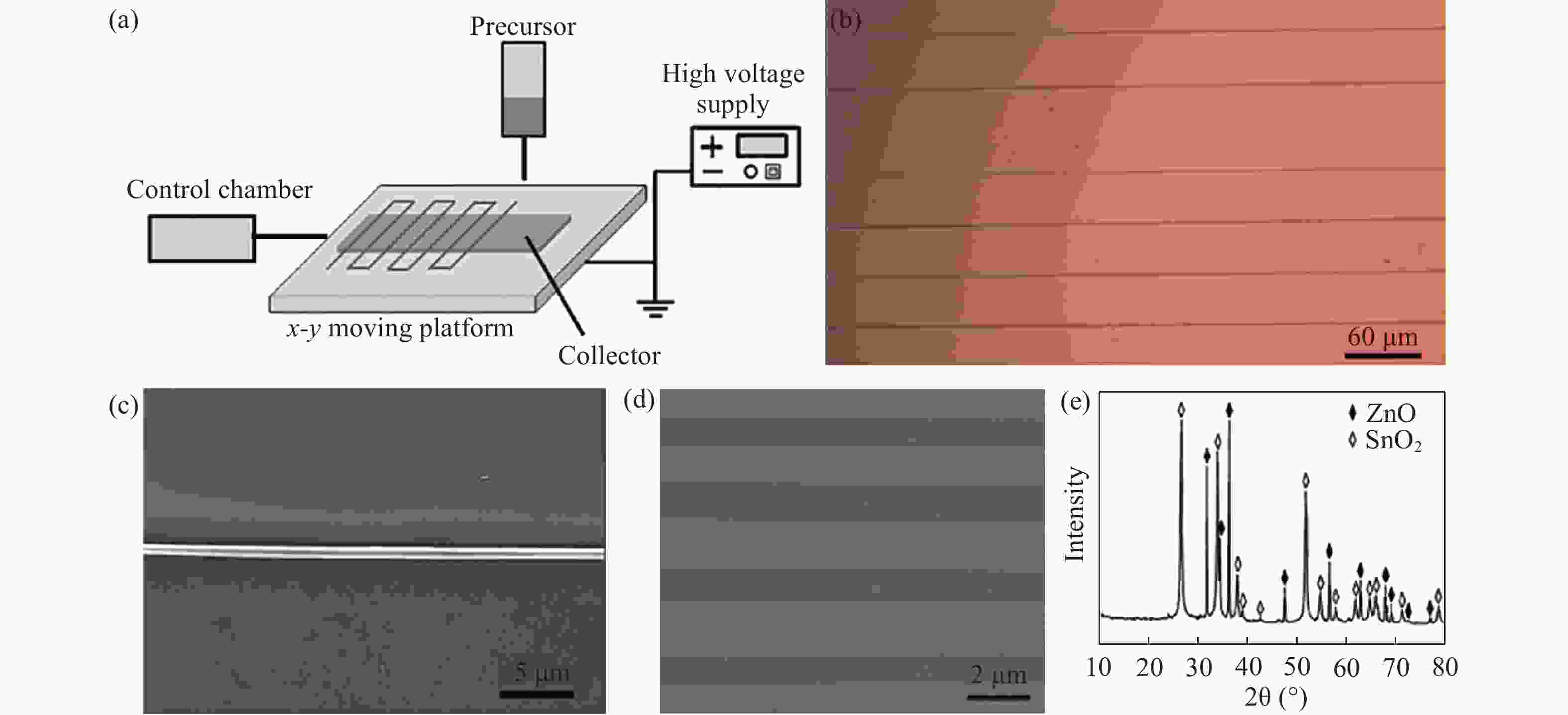
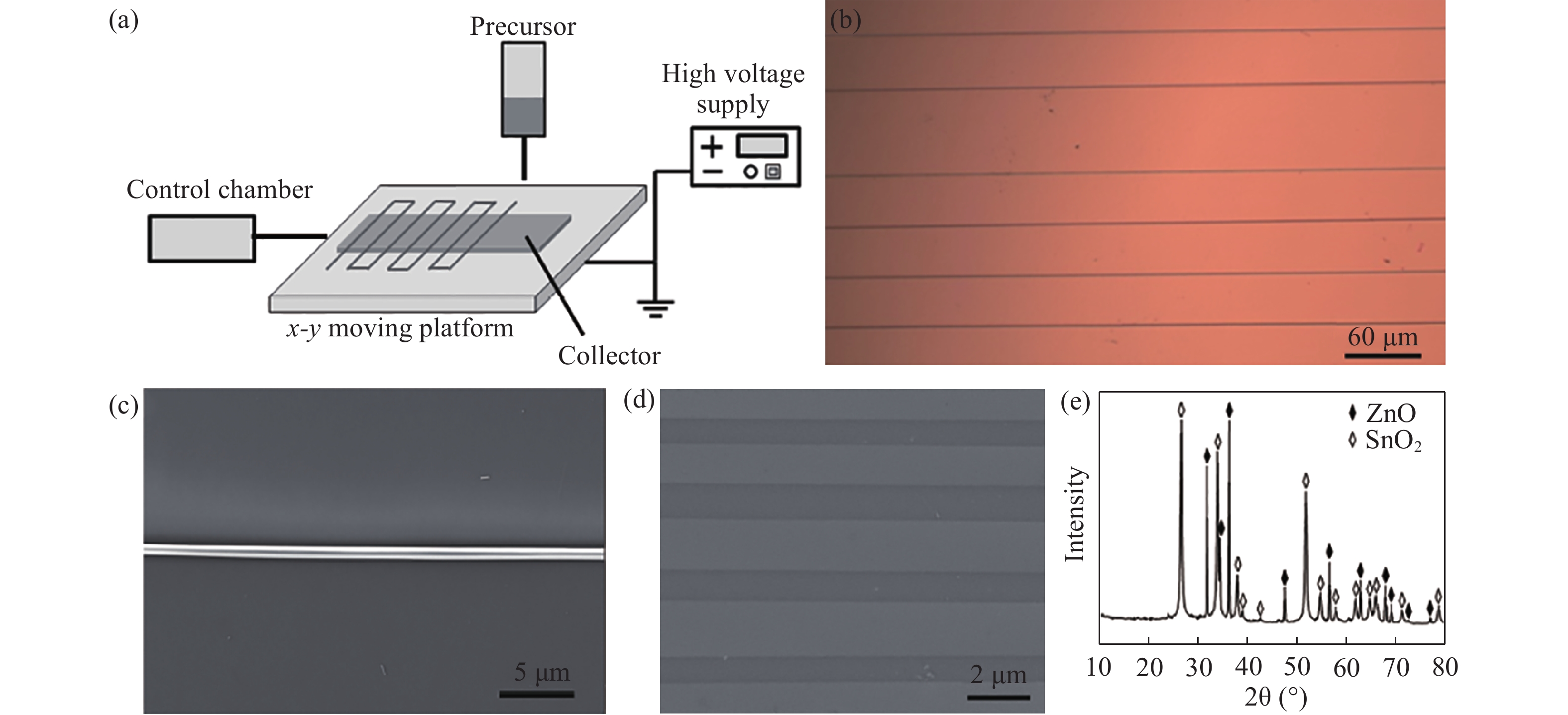
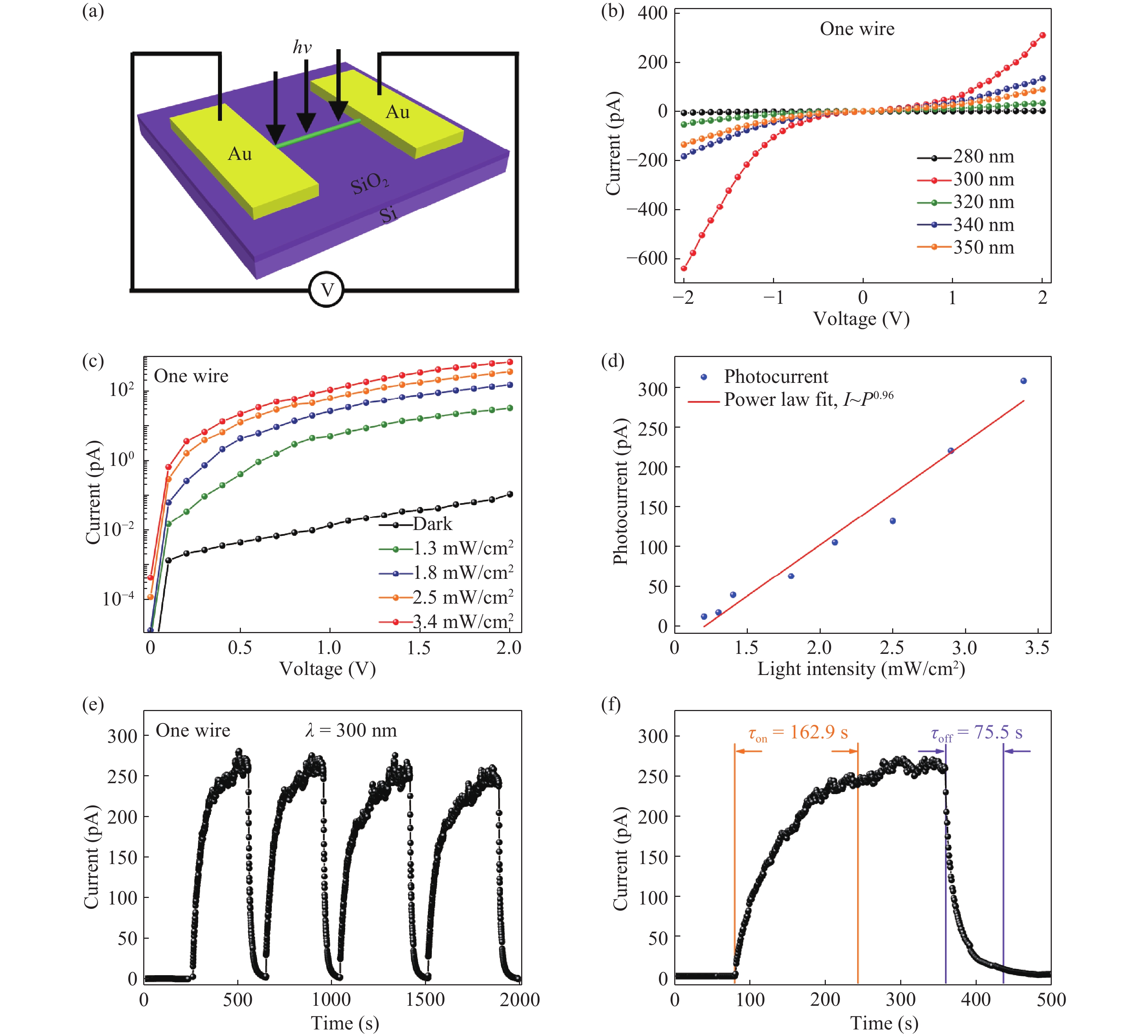
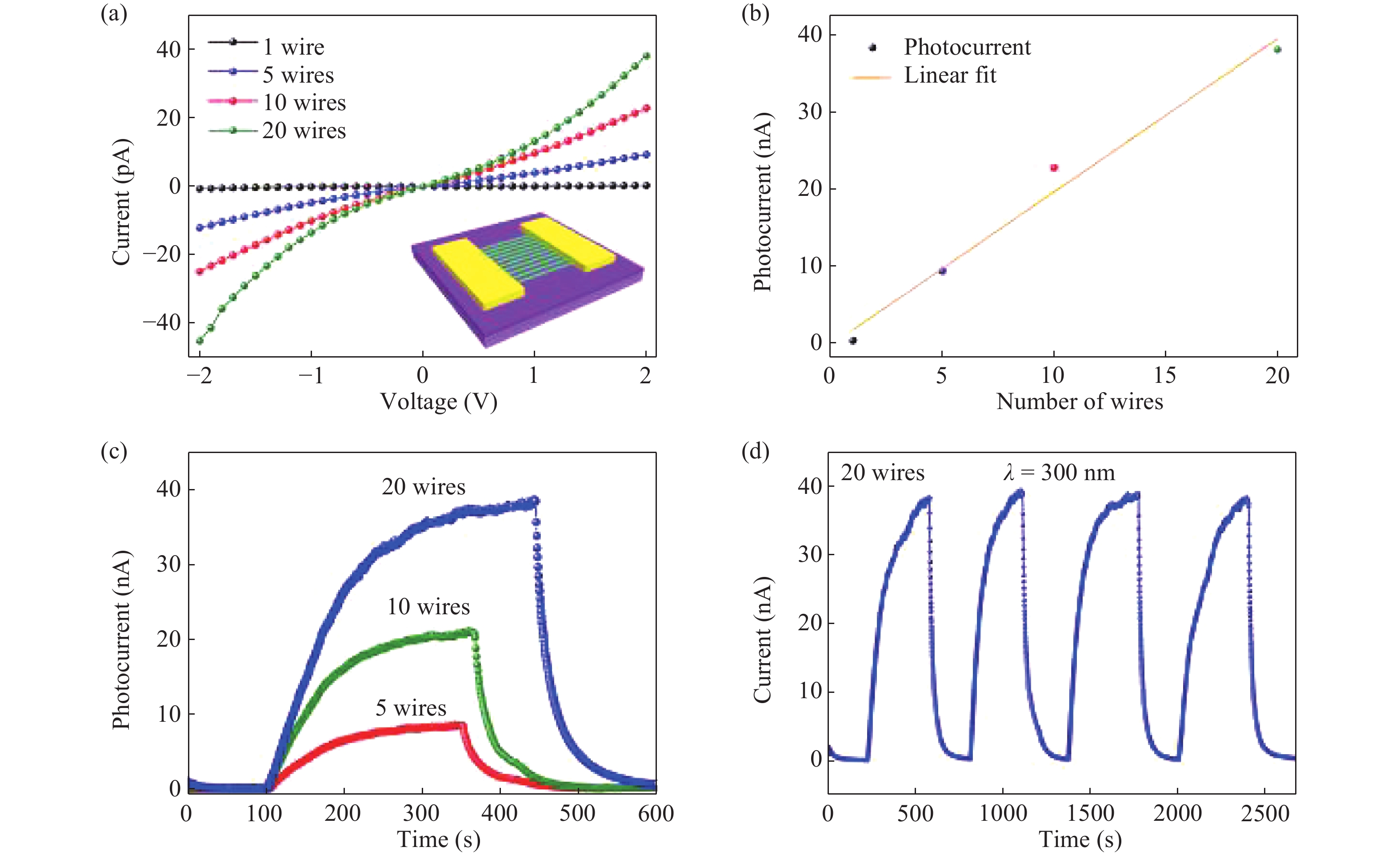
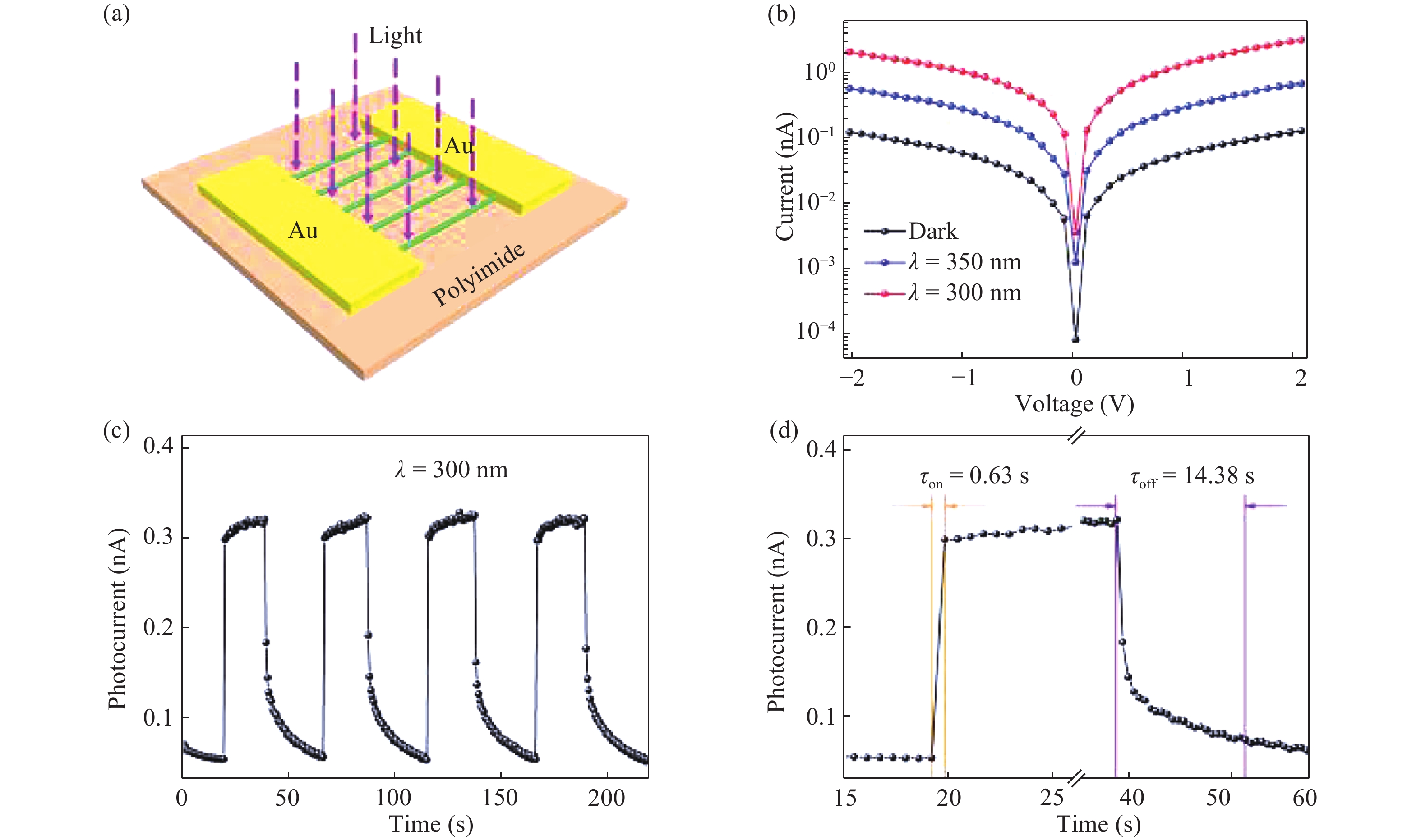
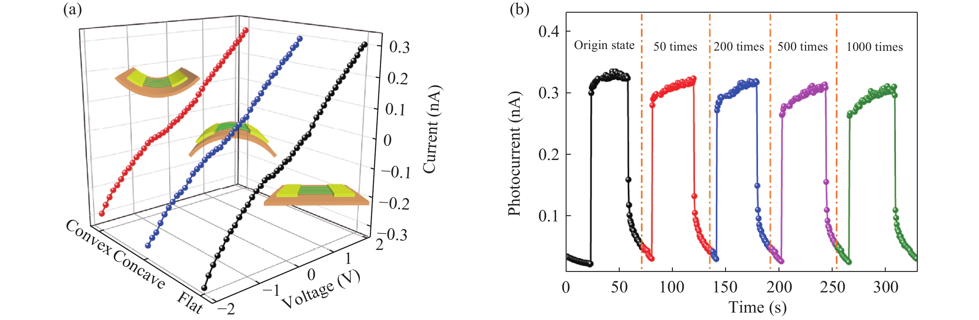
A ZnO–SnO2 nanowires (NWs) array, as a metal oxide semiconductor, was successfully synthesized by a near-field electrospinning method for the applications as high performance ultraviolet photodetectors. Ultraviolet photodetectors based on a single nanowire exhibited excellent photoresponse properties to 300 nm ultraviolet light illumination including ultrahigh Ion/Ioff ratios (up to 103), good stability and reproducibility because of the separation between photo-generated electron-hole pairs. Moreover, the NWs array shows an enhanced photosensing performance. Flexible photodetectors on the PI substrates with similar tendency properties were also fabricated. In addition, under various bending curvatures and cycles, the as-fabricated flexible photodetectors revealed mechanical flexibility and good stable electrical properties, showing that they have the potential for applications in future flexible photoelectron devices.
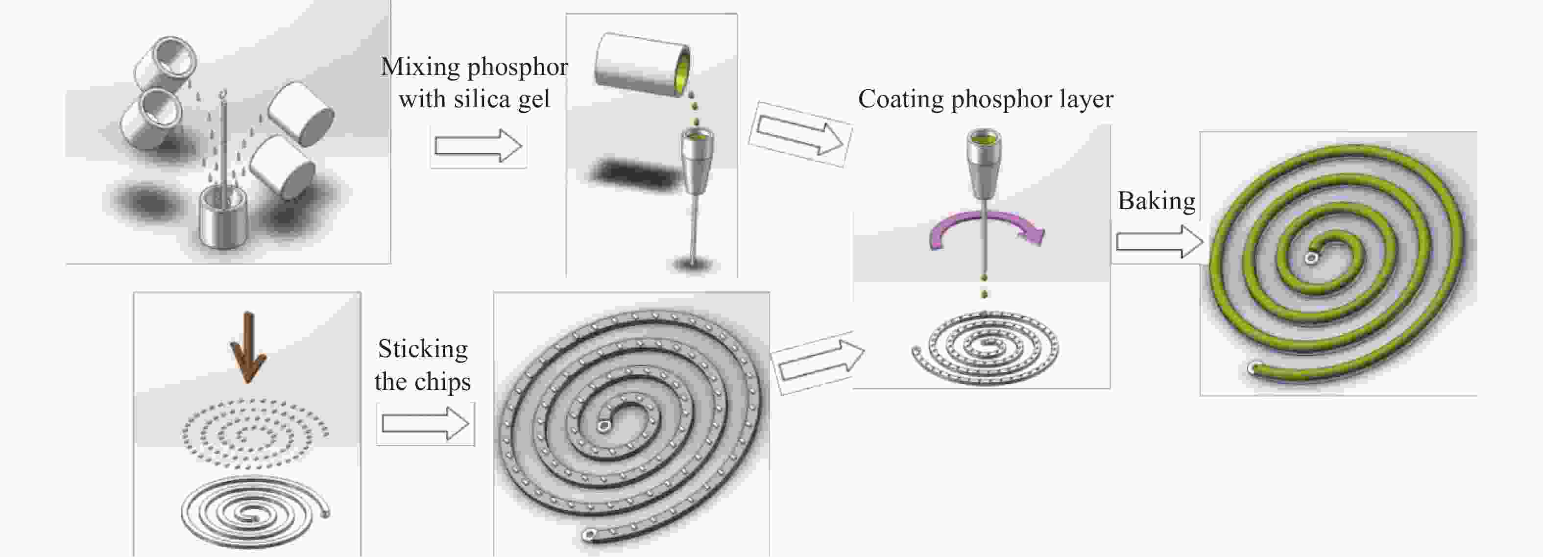
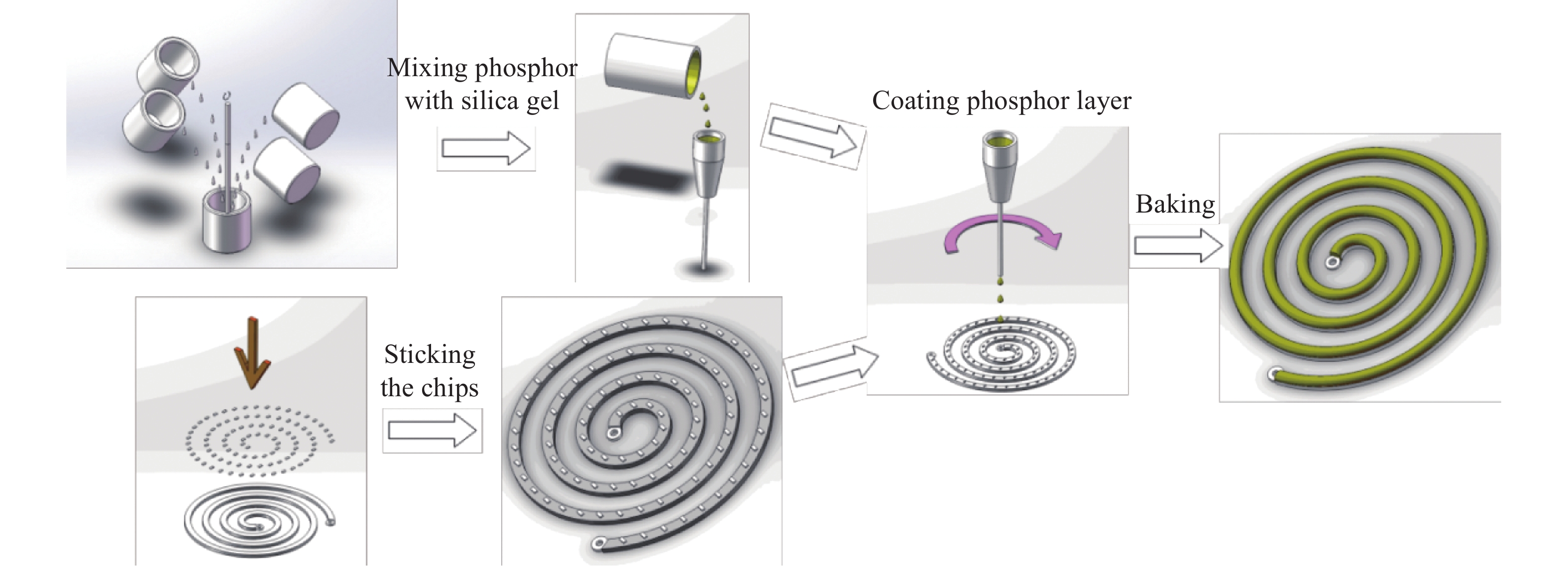
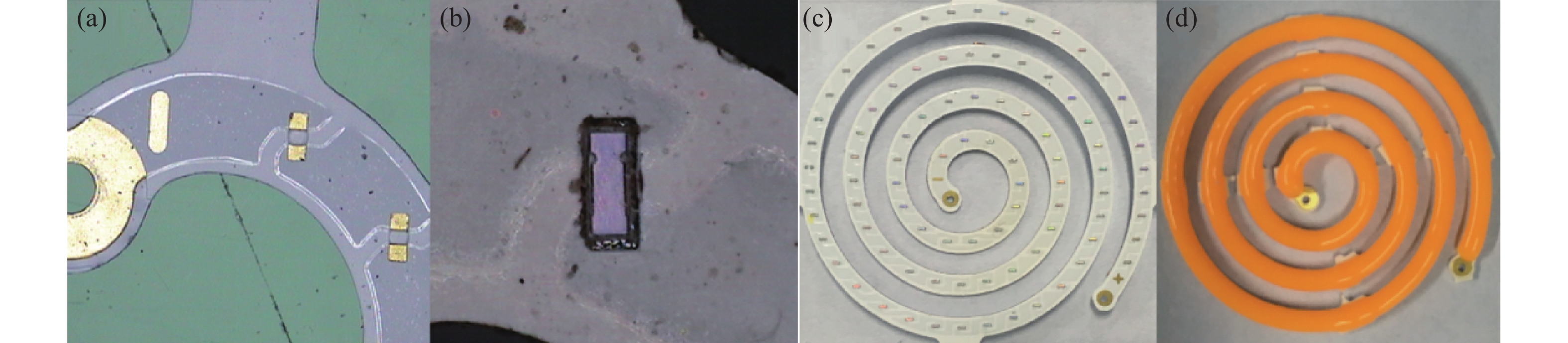
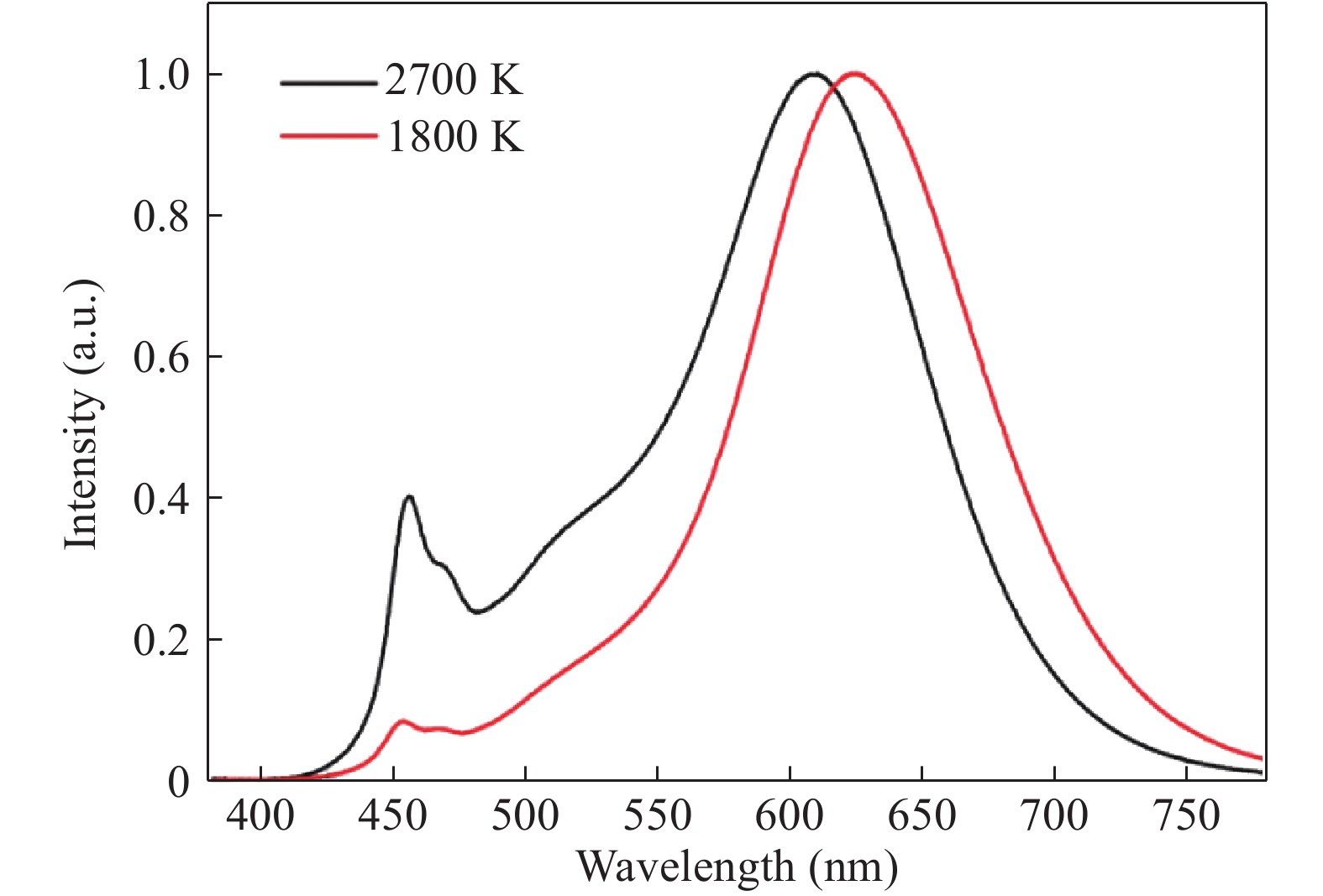
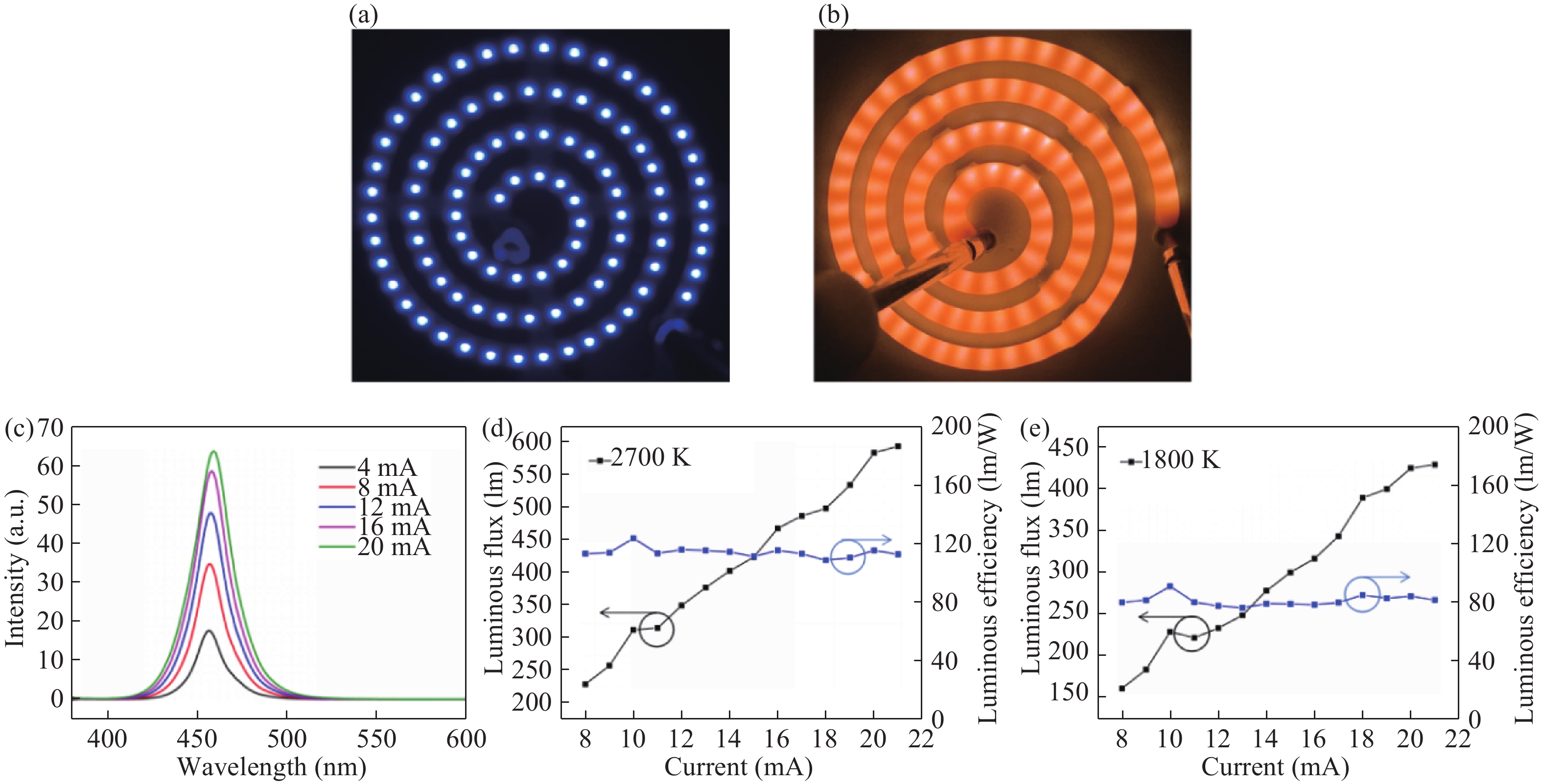
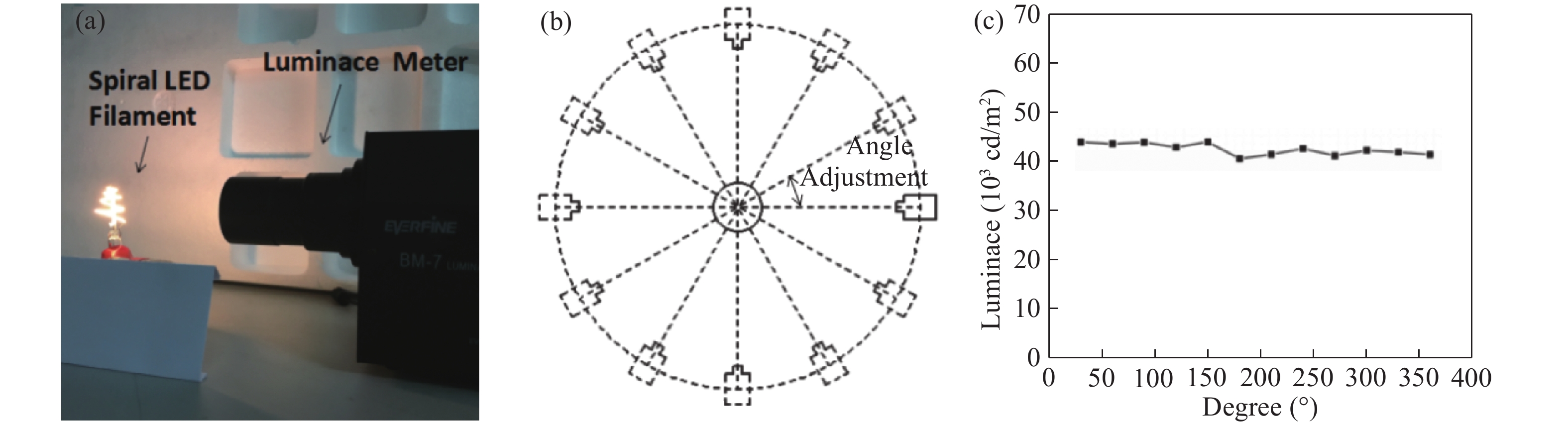
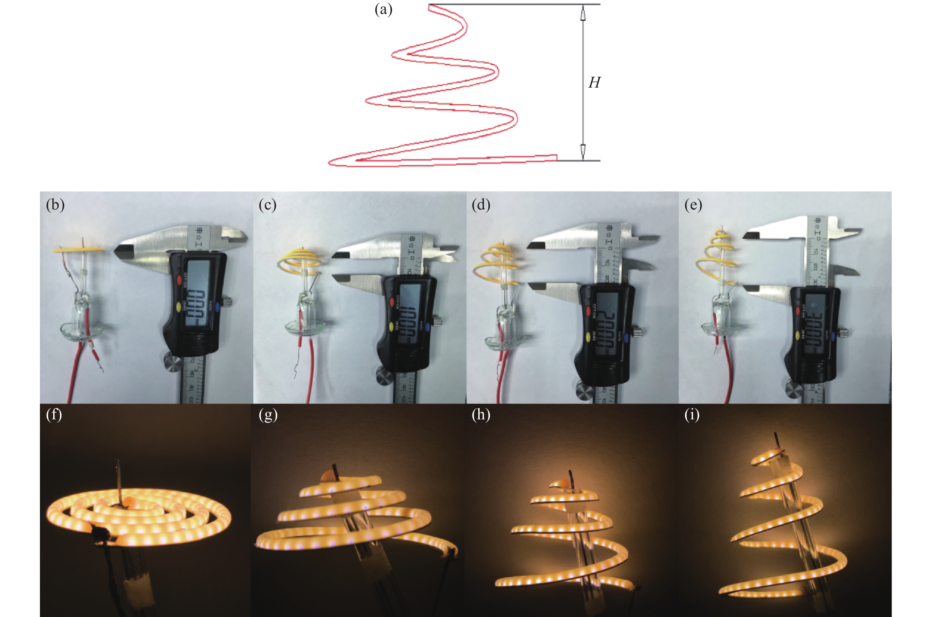
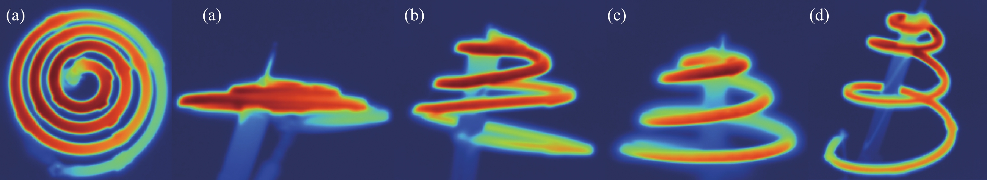
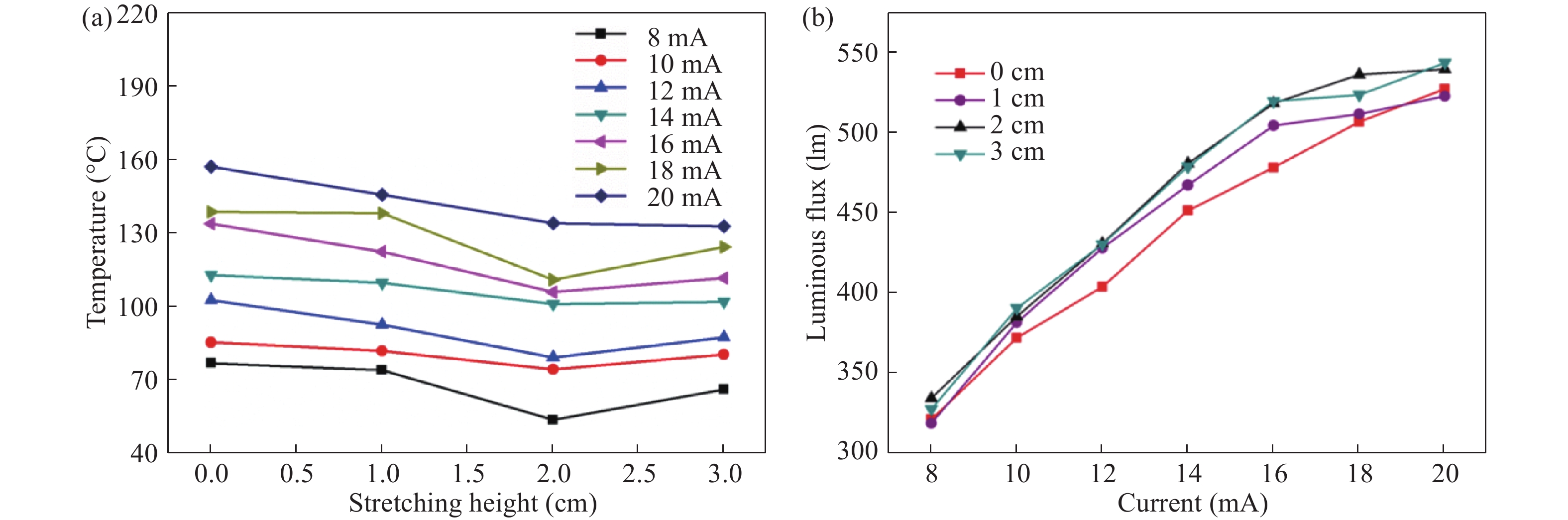
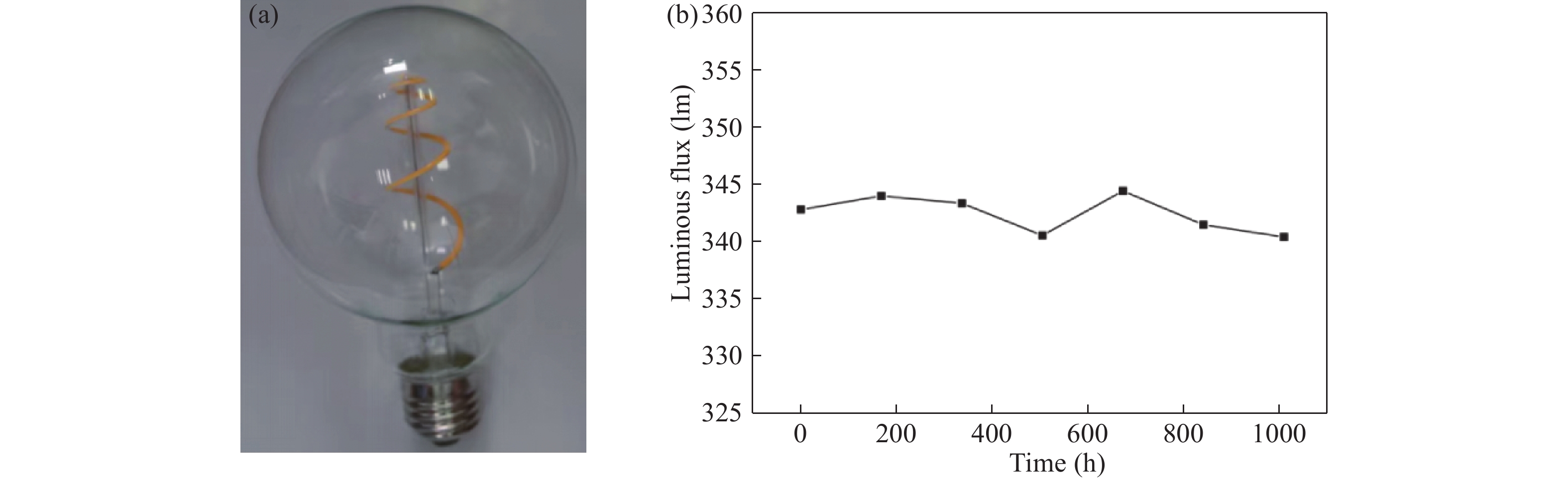
This paper introduces a new type of spiral white light-emitting diodes (WLED) filament with high luminous efficiency and uniform optical performance. The optical and thermal properties of the flexible filament were investigated at different stretching heights, namely 0, 1, 2, and 3 cm. The results indicated that the filament showed the best optical characteristics at the stretching height of 2 cm, because of good heat dissipation. In addition, the radiation temperature of the filament was inversely proportional to the output luminous flux. The reliability of the filament at a stretching height of 2 cm was also evaluated after 1000 h of use. The result demonstrated that the luminous flux decay of the bulb was only 0.85%. The flexible spiral WLED filament exhibiting high luminous flux and good reliability could be adapted to promote industrial development in the near future.

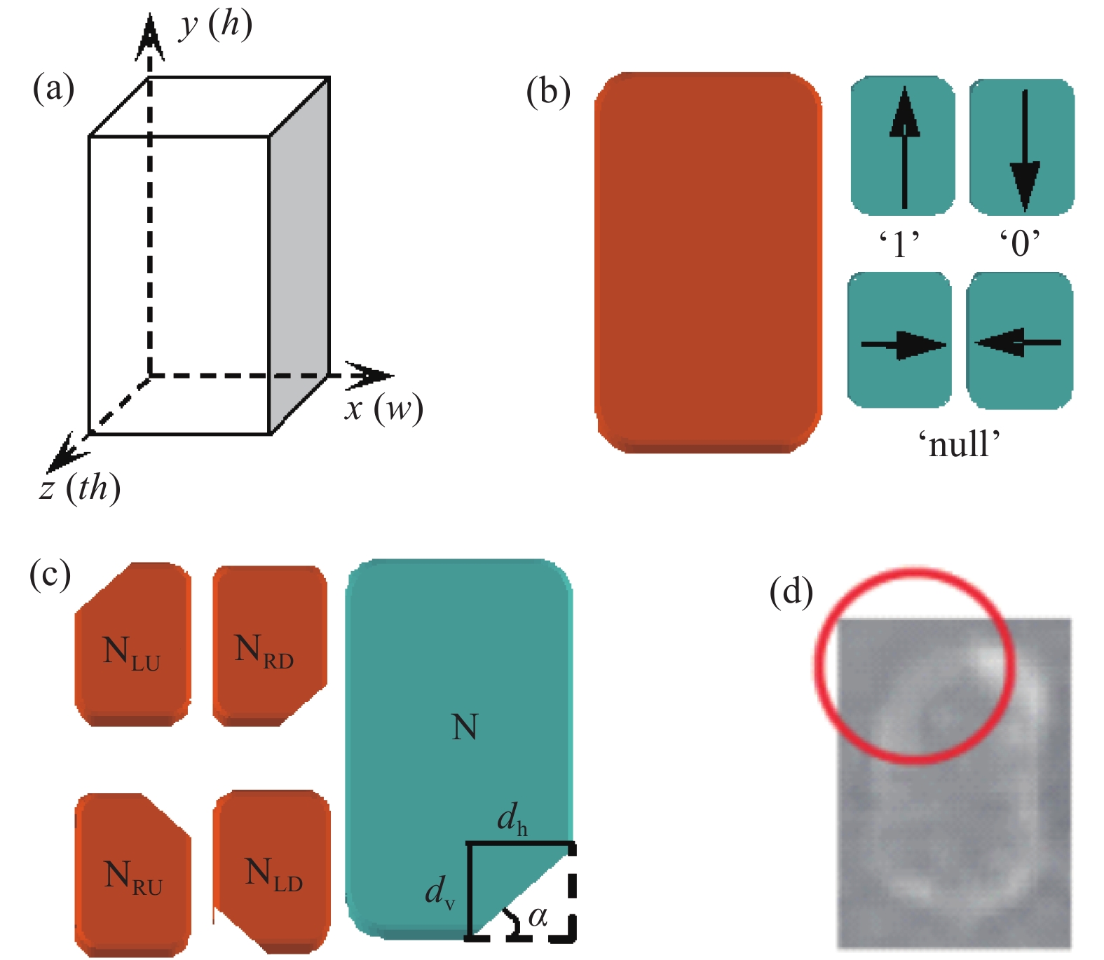
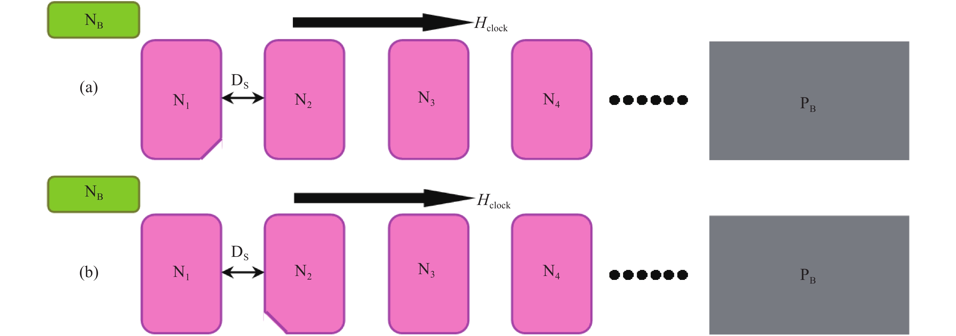
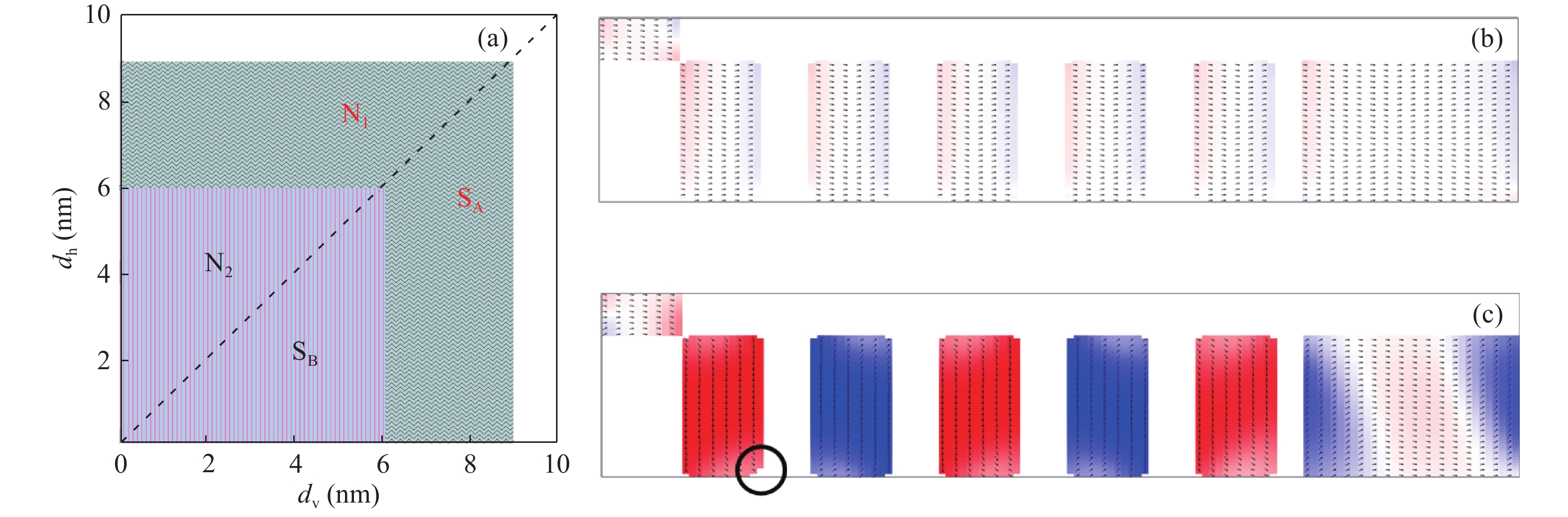
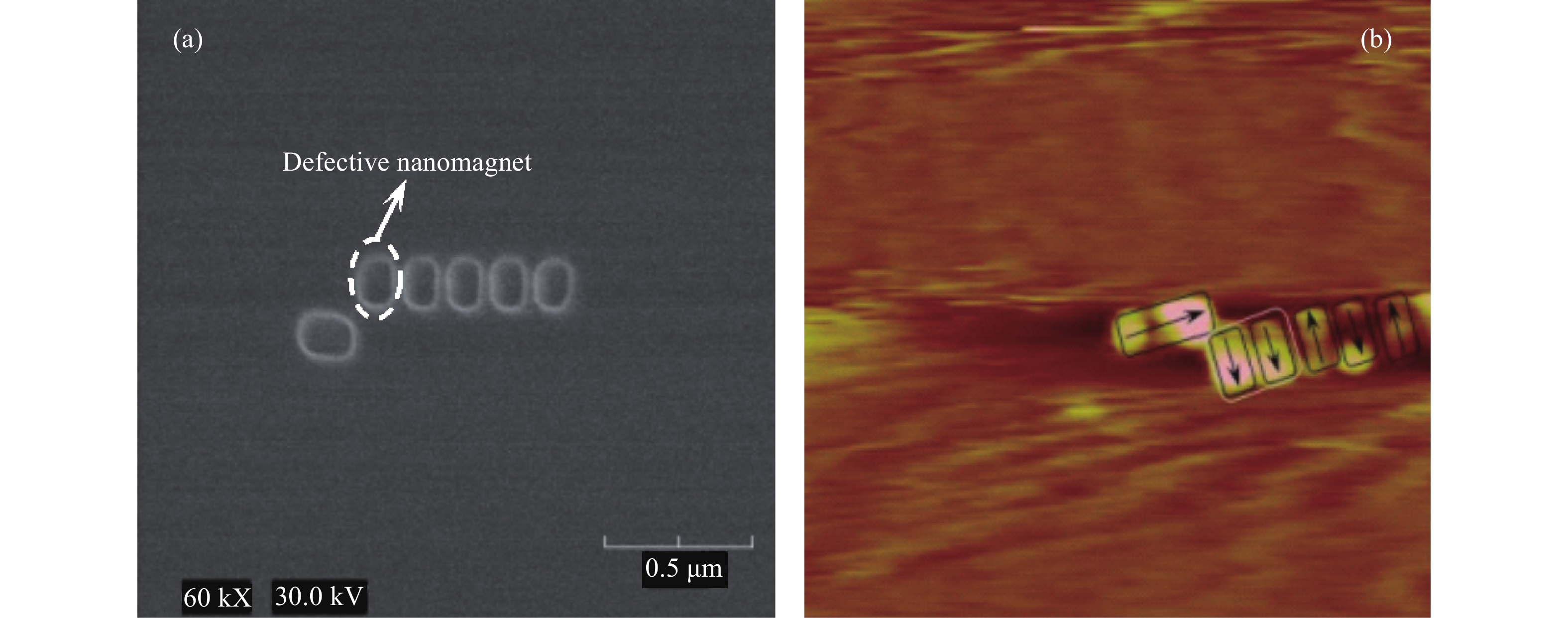
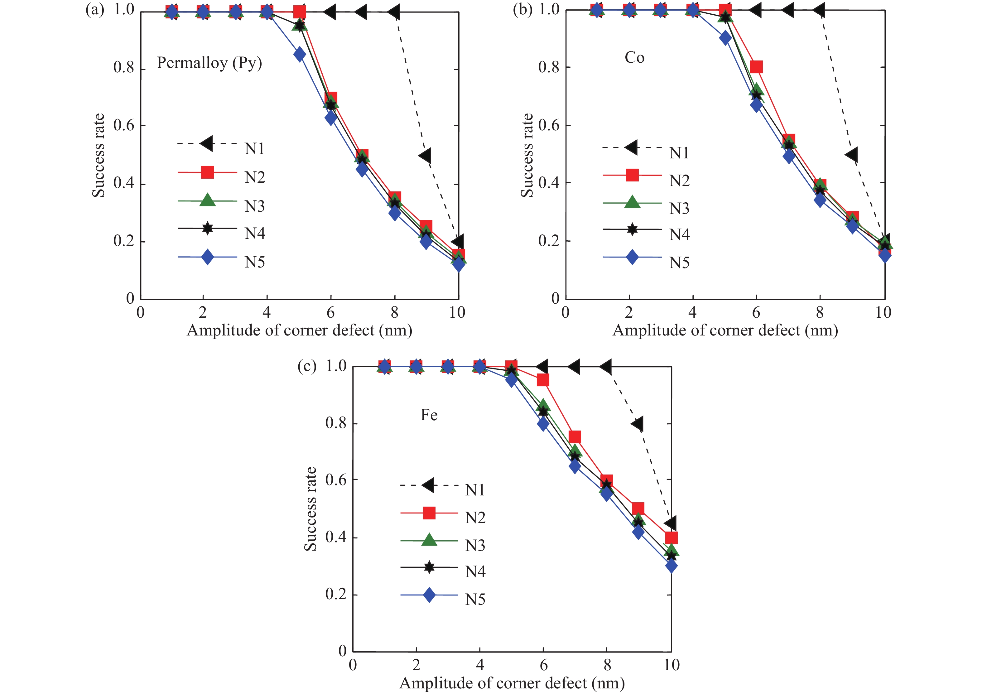
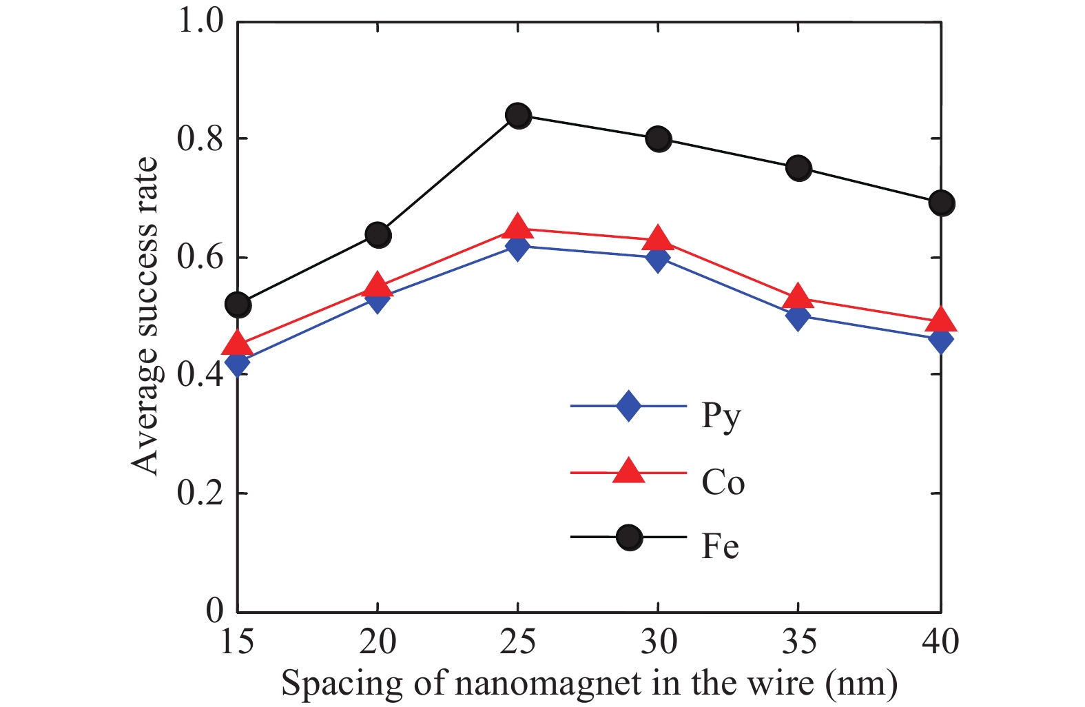
Nanomagnet logic (NML) devices have been proposed as one of the best candidates for the next generation of integrated circuits thanks to its substantial advantages of nonvolatility, radiation hardening and potentially low power. In this article, errors of nanomagnetic interconnect wire subjected to magnet edge imperfections have been evaluated for the purpose of reliable logic propagation. The missing corner defects of nanomagnet in the wire are modeled with a triangle, and the interconnect fabricated with various magnetic materials is thoroughly investigated by micromagnetic simulations under different corner defect amplitudes and device spacings. The results show that as the defect amplitude increases, the success rate of logic propagation in the interconnect decreases. More results show that from the interconnect wire fabricated with materials, iron demonstrates the best defect tolerance ability among three representative and frequently used NML materials, also logic transmission errors can be mitigated by adjusting spacing between nanomagnets. These findings can provide key technical guides for designing reliable interconnects.

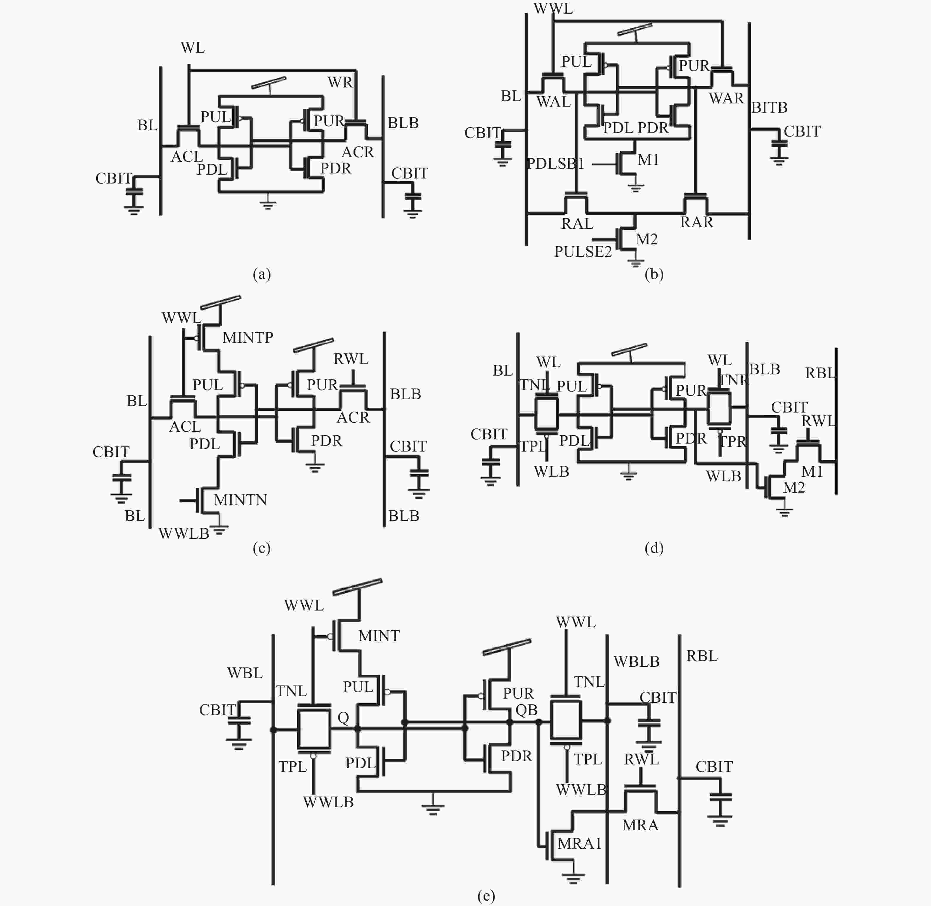
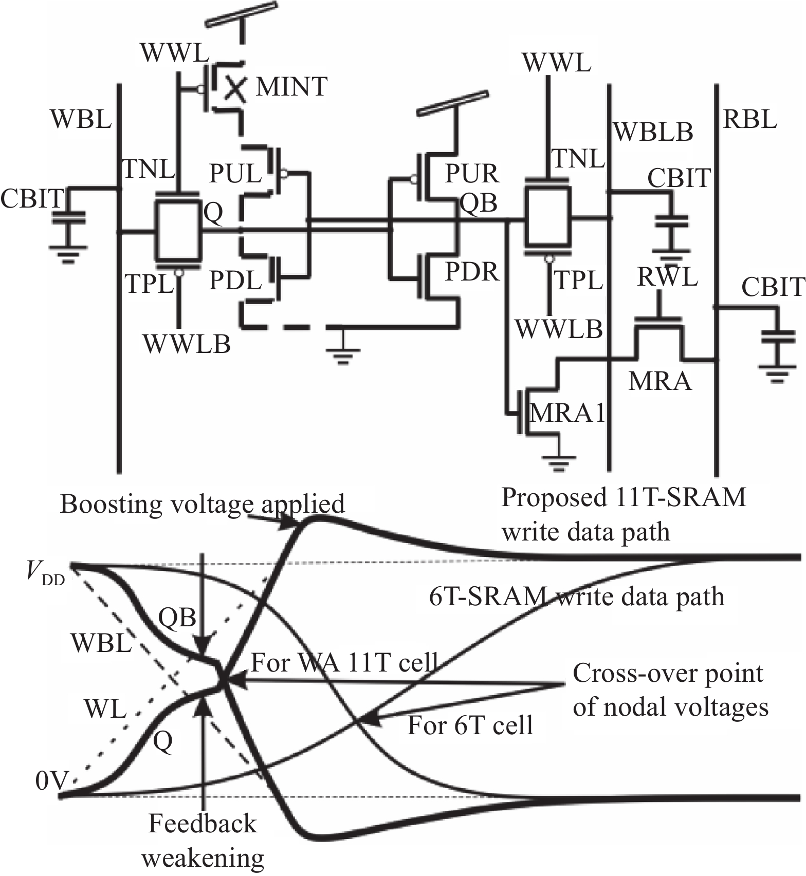
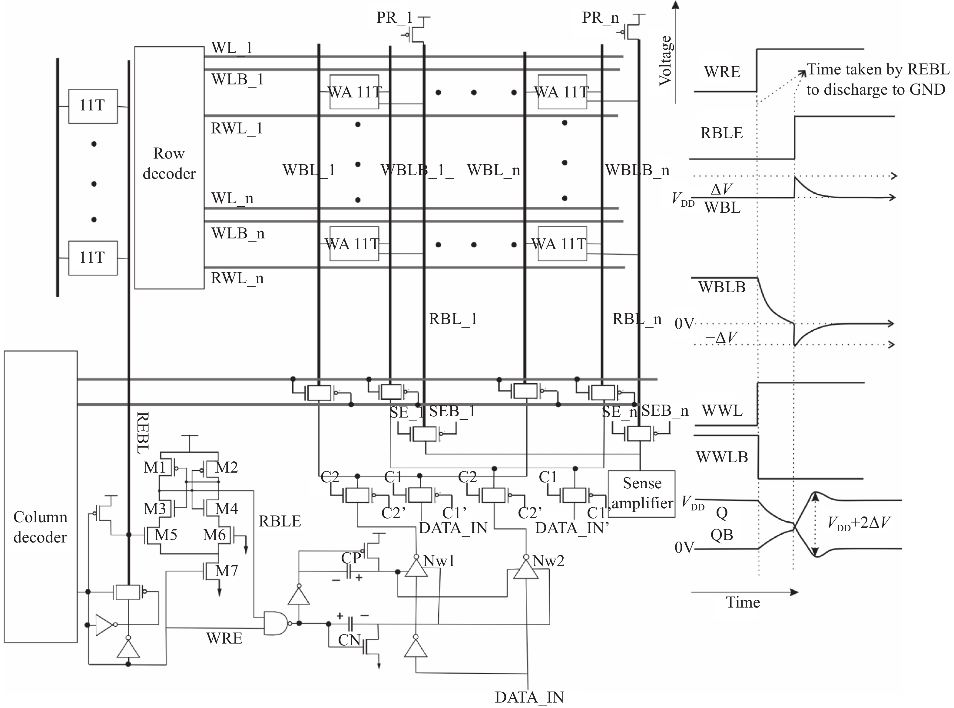
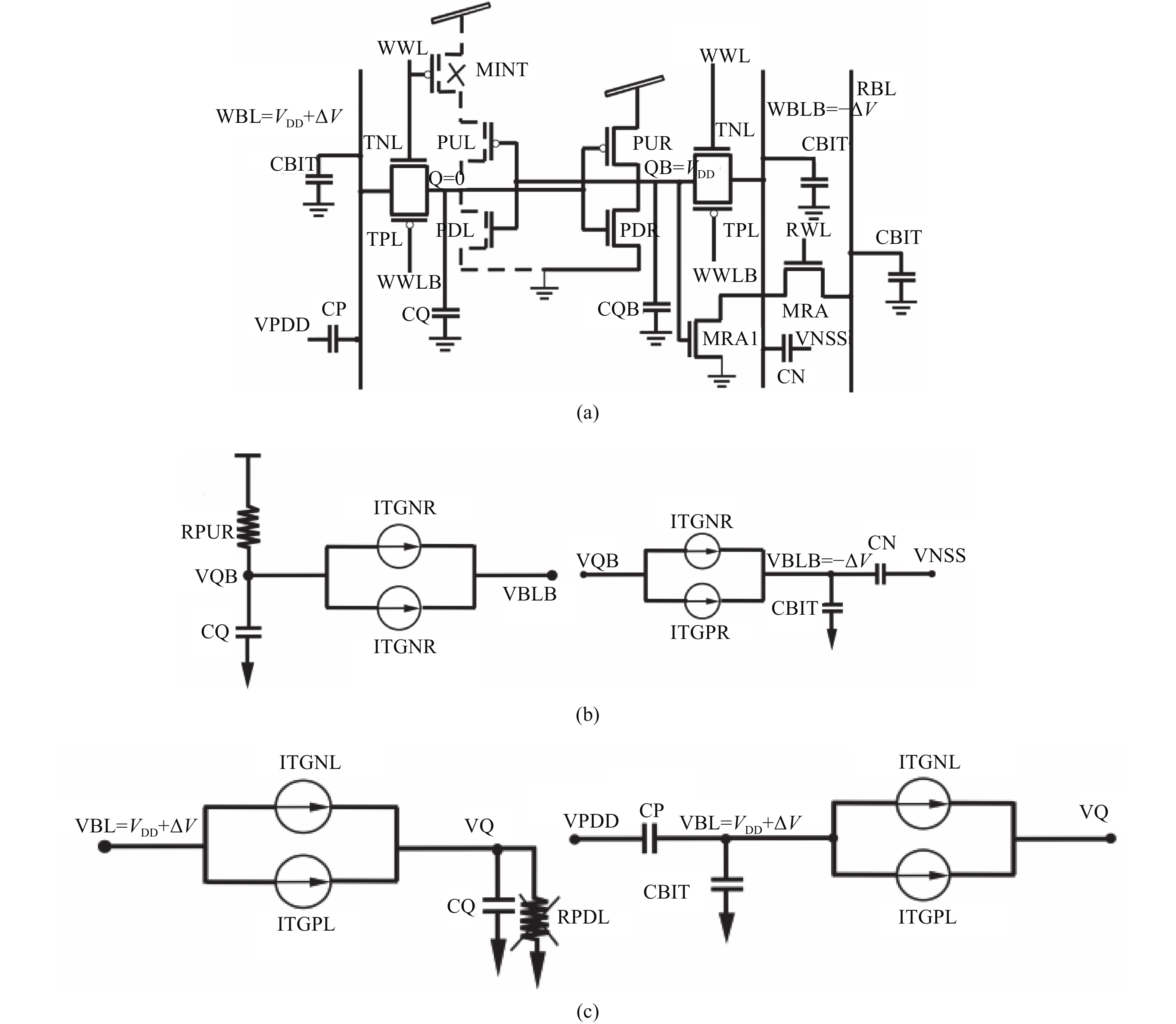
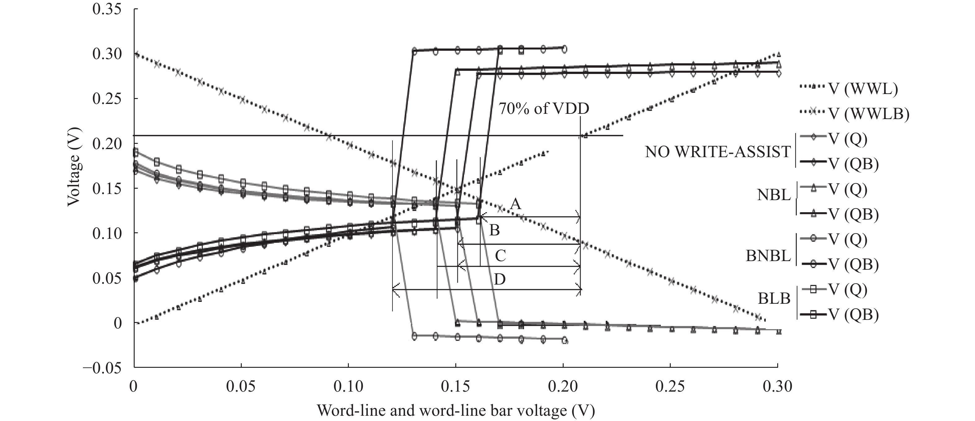
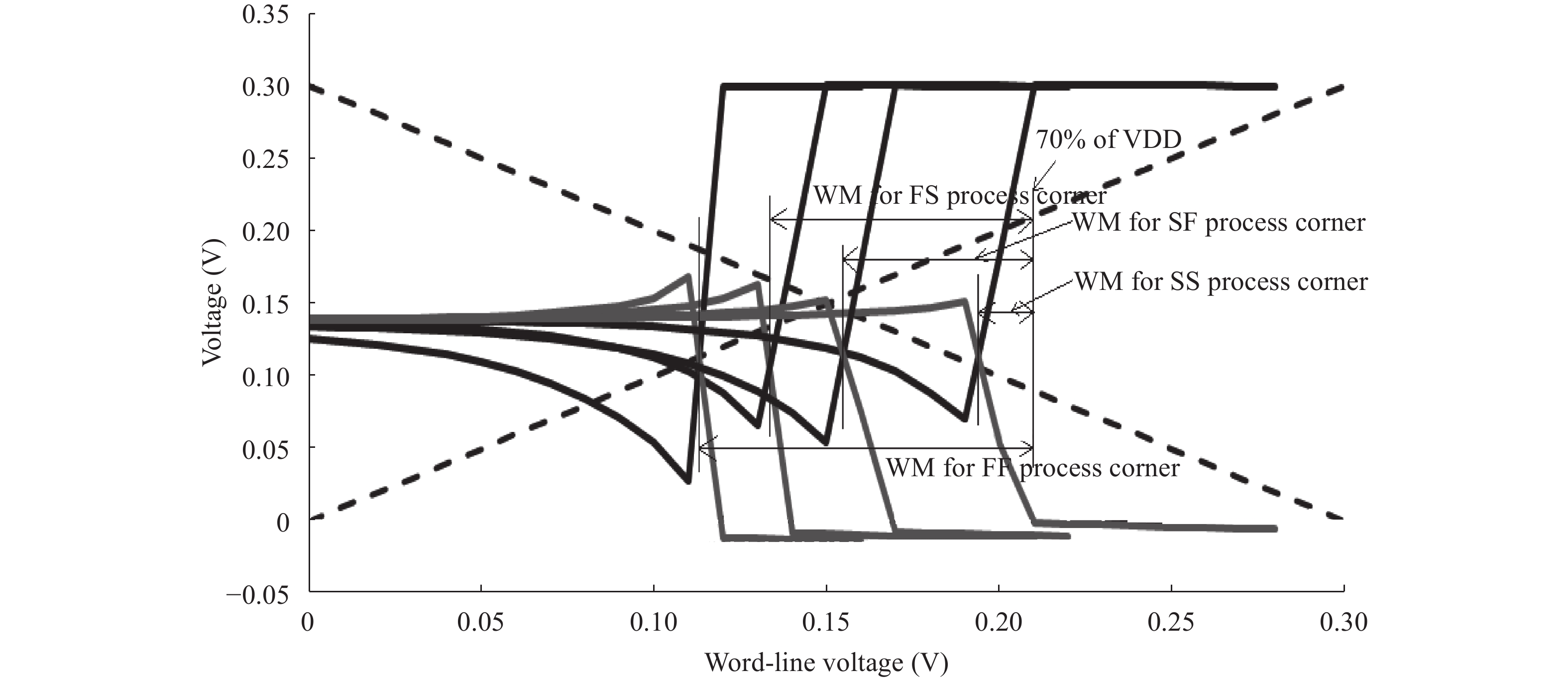
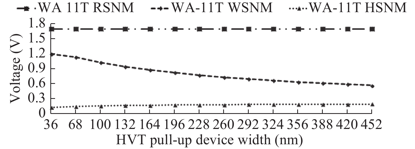
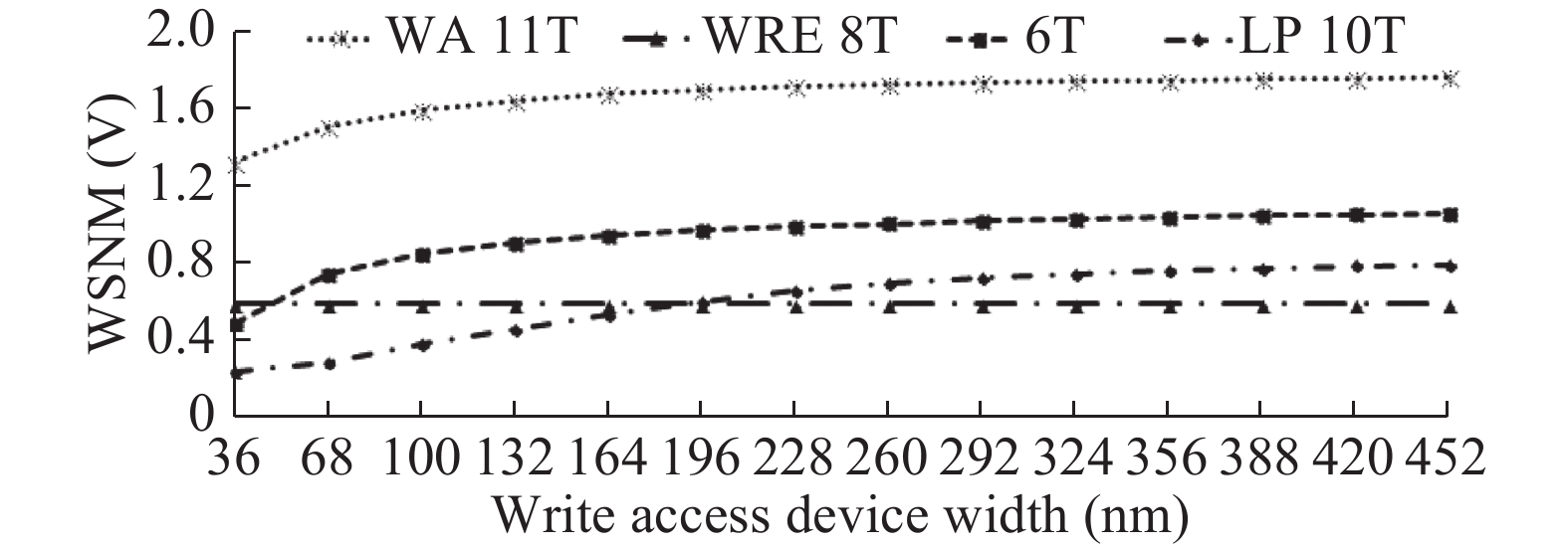
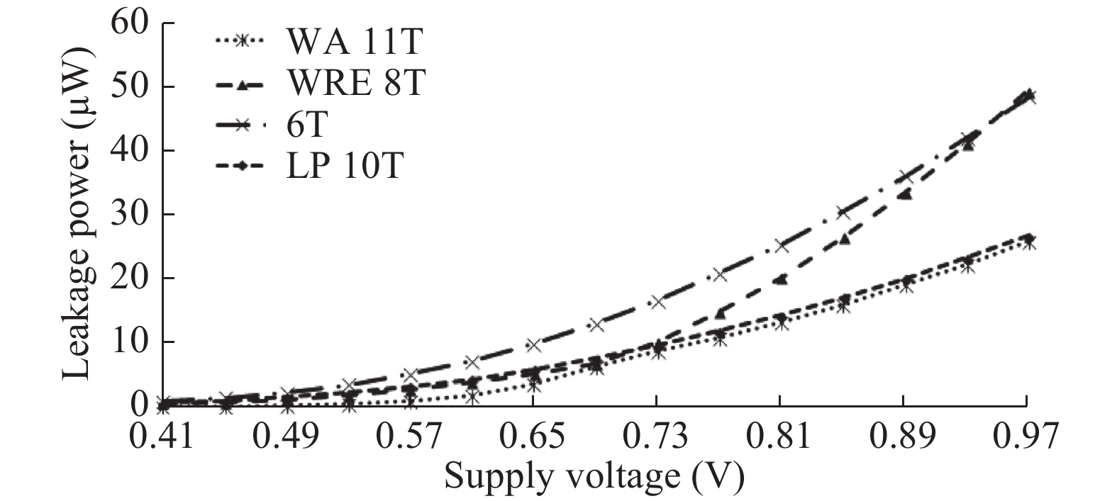
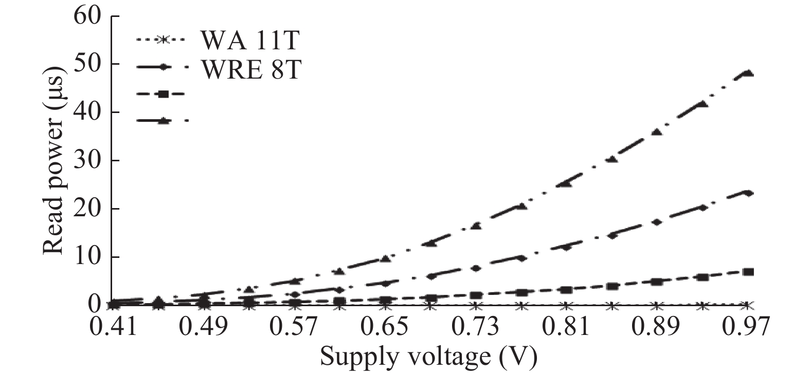
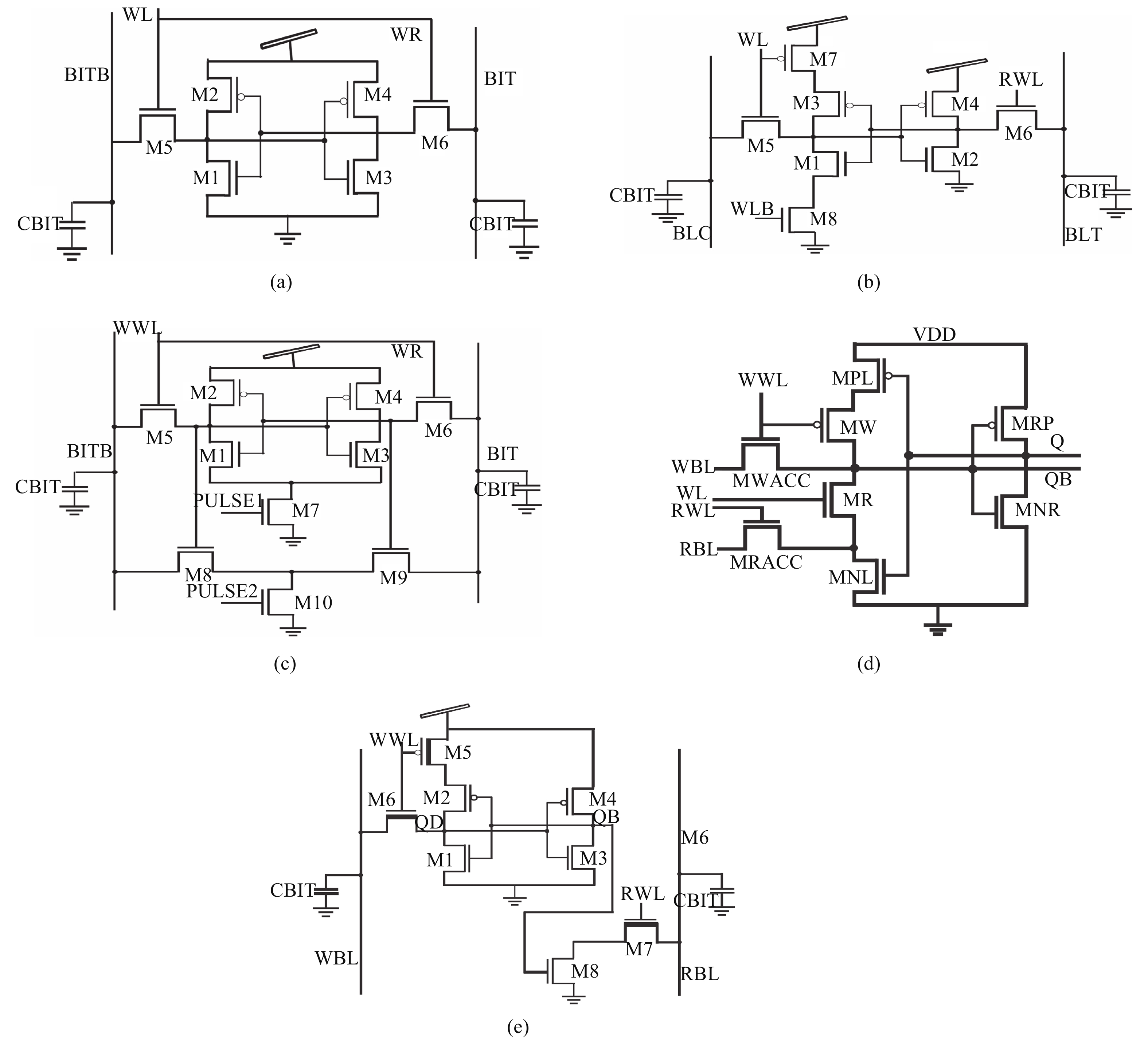
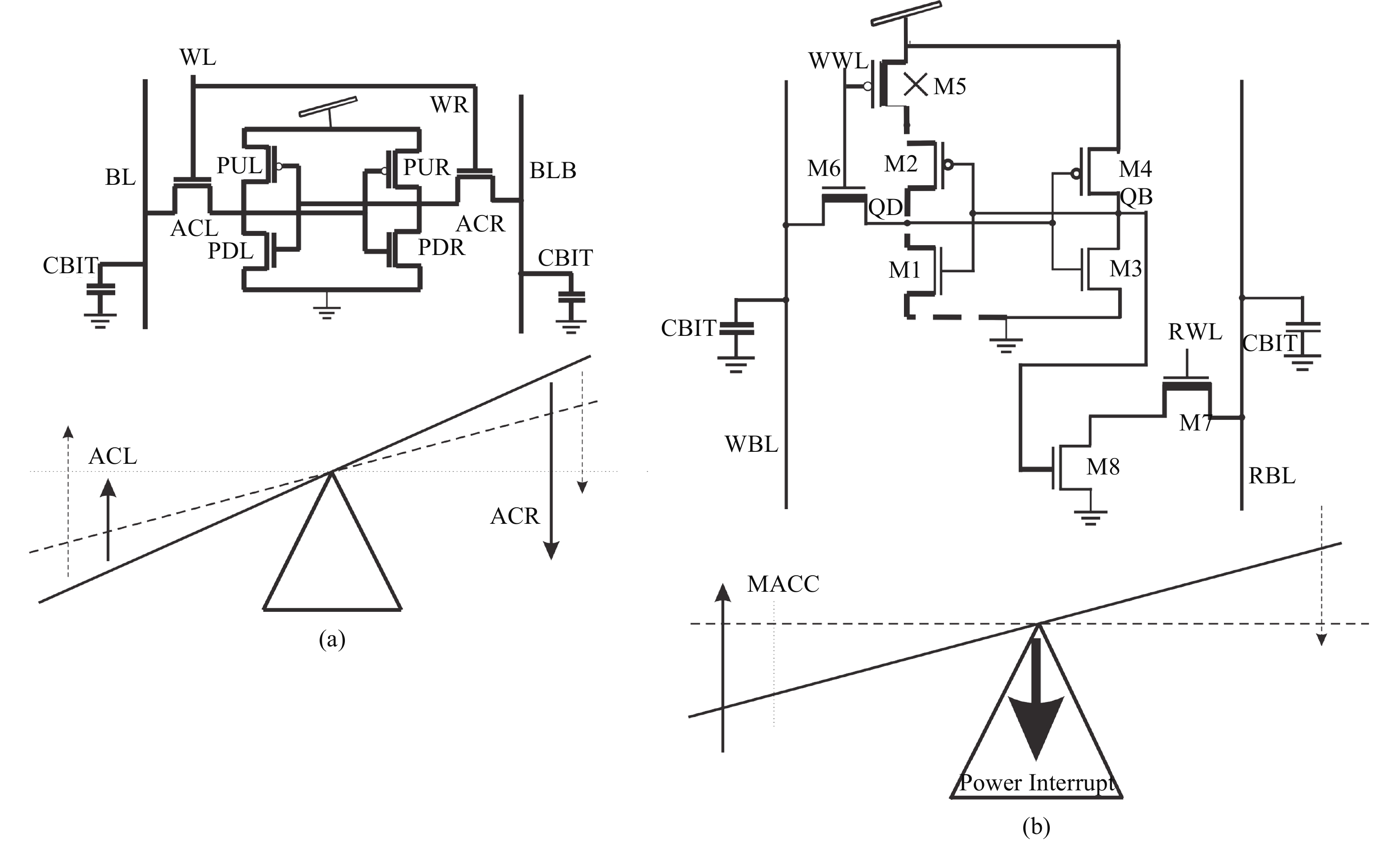
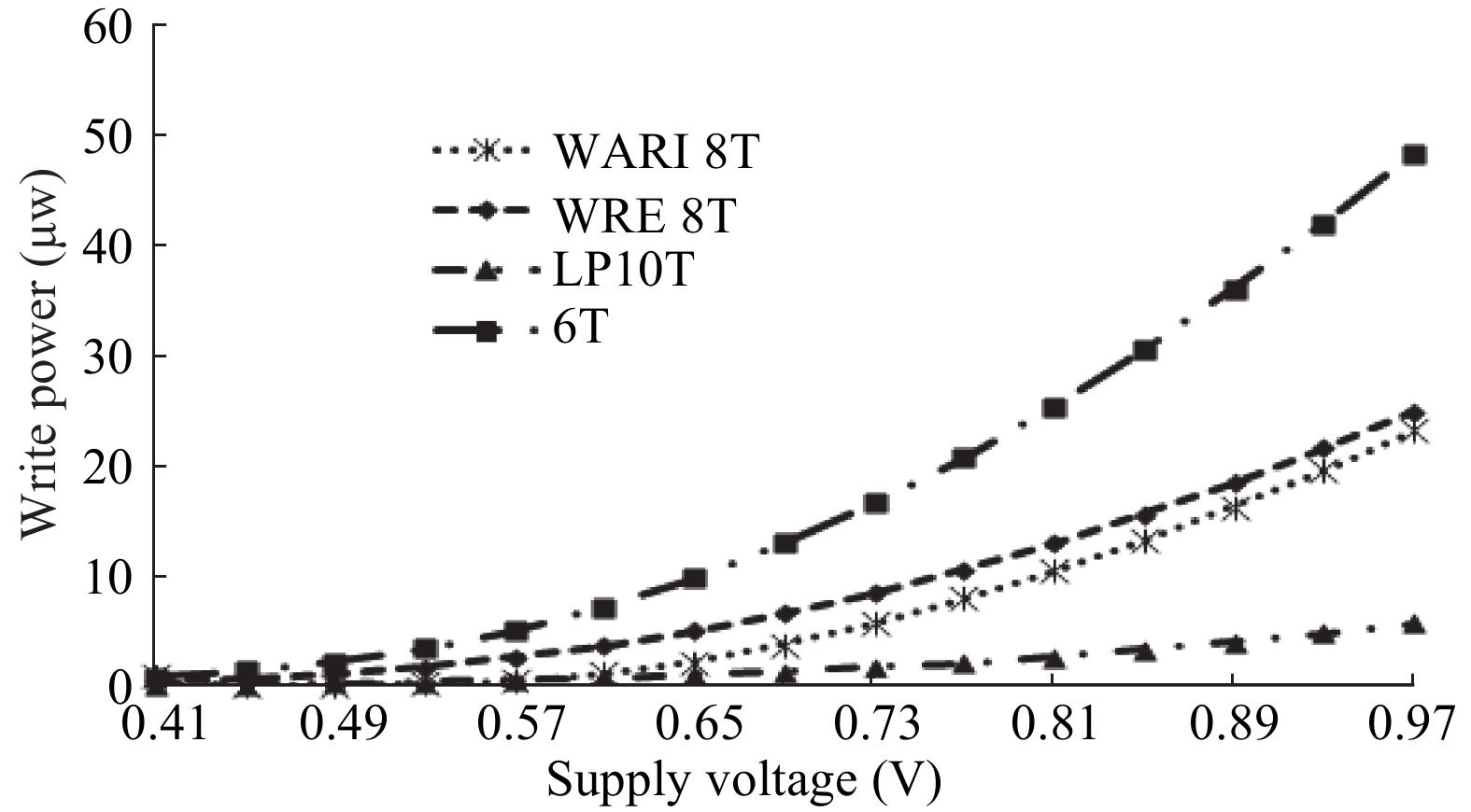
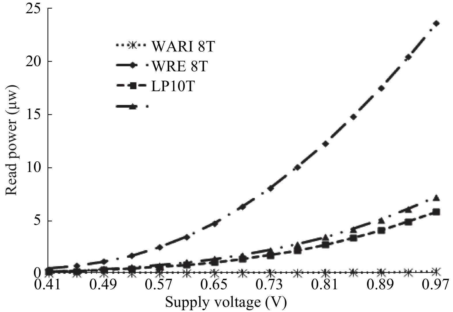
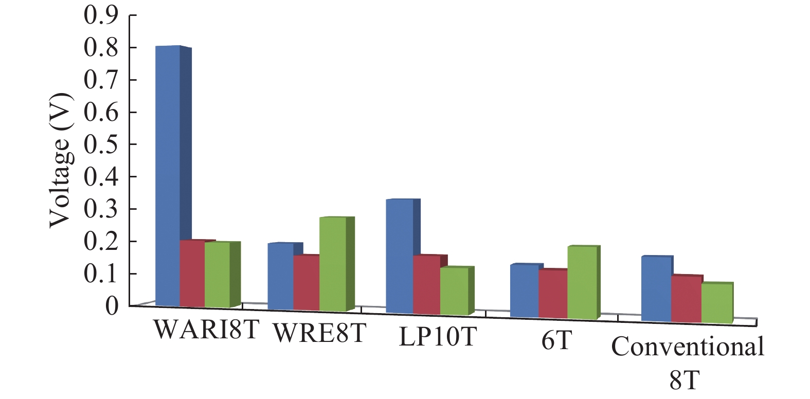
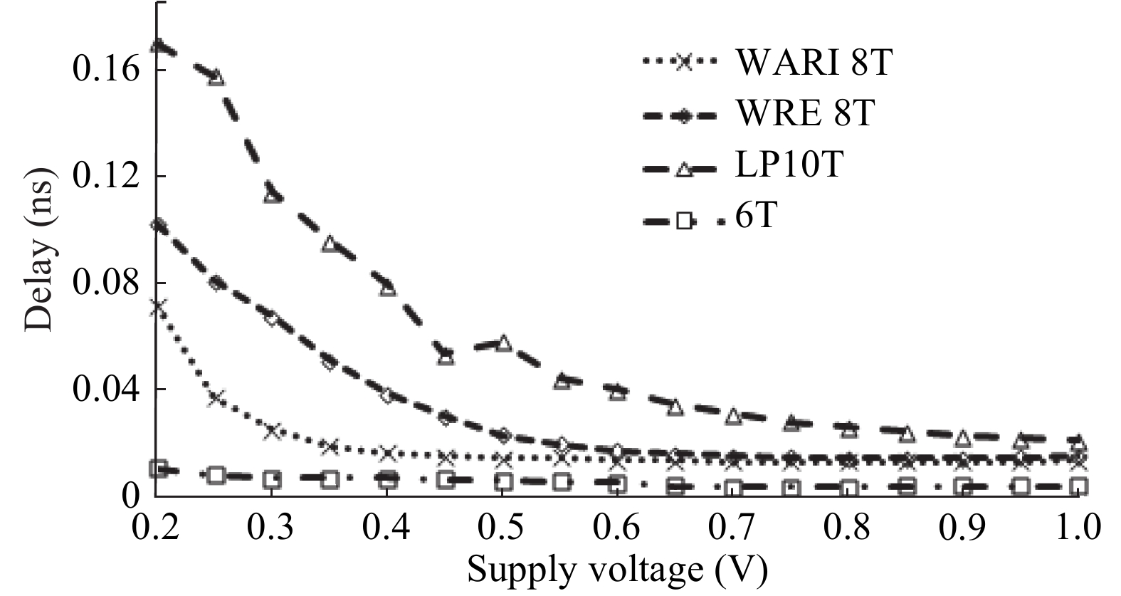
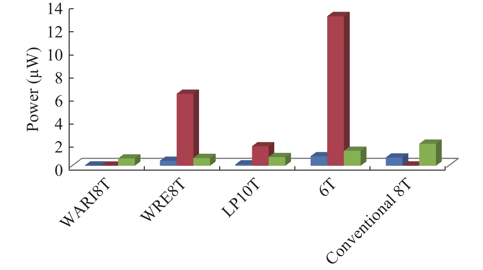
A new 11 T SRAM cell with write-assist is proposed to improve operation at low supply voltage. In this technique, a negative bit-line voltage is applied to one of the write bit-lines, while a boosted voltage is applied to the other write bit-line where transmission gate access is used in proposed 11 T cell. Supply voltage to one of the inverters is interrupted to weaken the feedback. Improved write feature is attributed to strengthened write access devices and weakened feedback loop of cell at the same time. Amount of boosting required for write performance improvement is also reduced due to feedback weakening, solving the persistent problem of half-selected cells and reliability reduction of access devices with the other suggested boosted and negative bit-line techniques. The proposed design improves write time by 79%, 63% and slower by 52% with respect to LP 10 T, WRE 8 T and 6 T cells respectively. It is found that write margin for the proposed cell is improved by about 4×, 2.4× and 5.37× compared to WRE8 T, LP10 T and 6 T respectively. The proposed cell with boosted negative bit line (BNBL) provides 47%, 31%, and 68.4% improvement in write margin with respect to no write-assist, negative bit line (NBL) and boosted bit line (BBL) write-assist respectively. Also, new sensing circuit with replica bit-line is proposed to give a more precise timing of applying boosted voltages for improved results. All simulations are done on TSMC 45 nm CMOS technology.
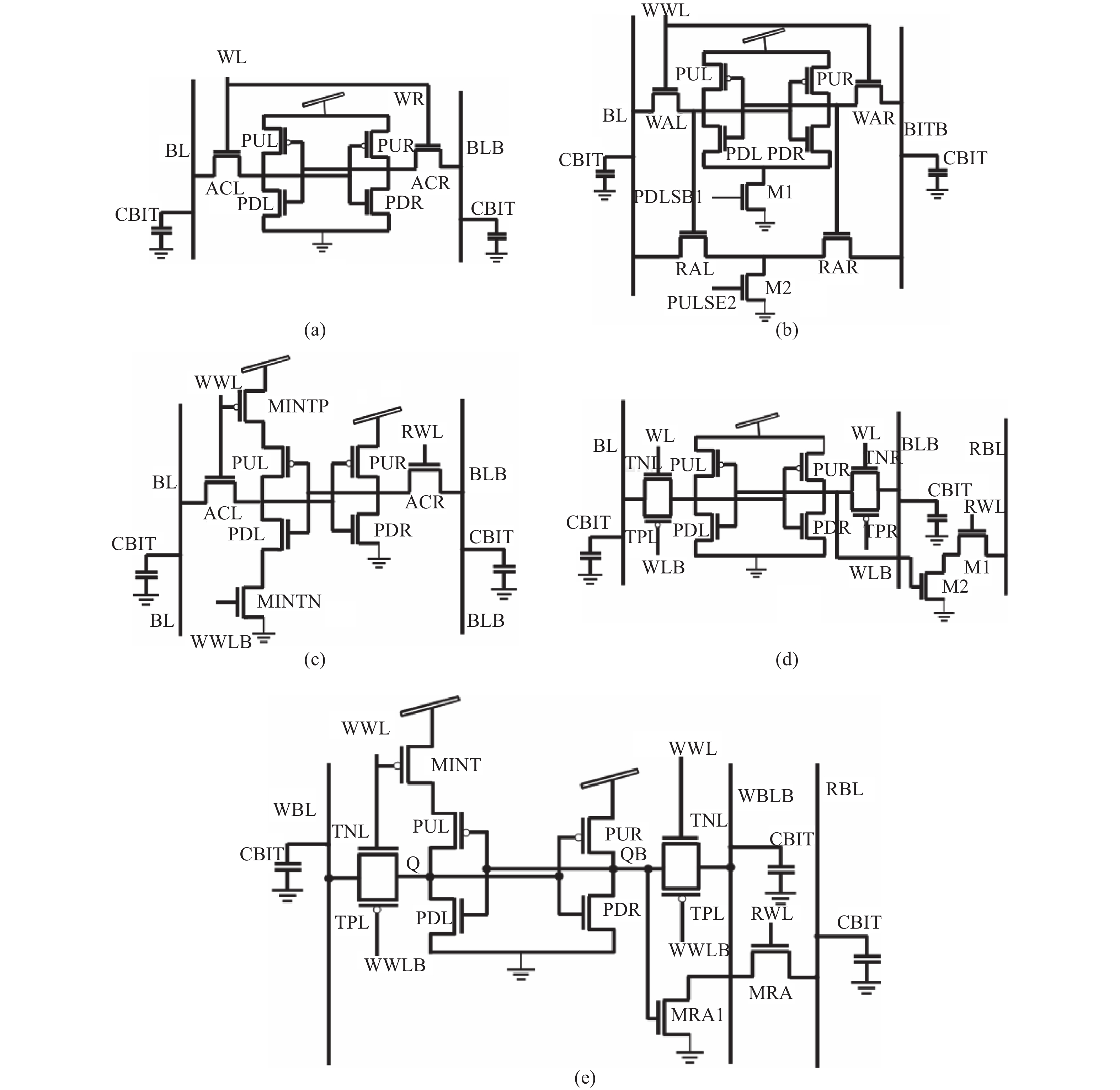


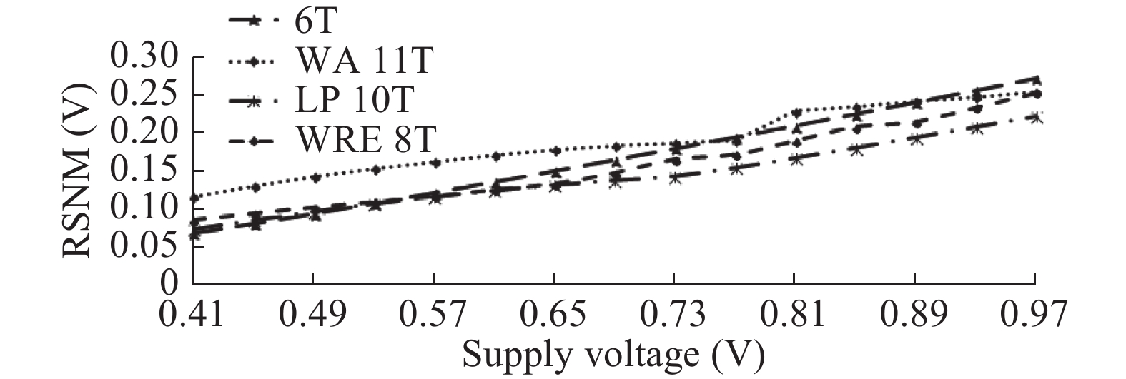
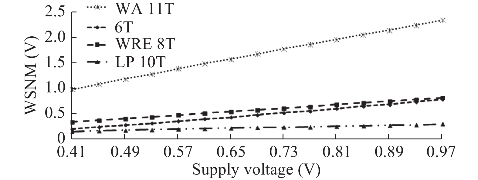

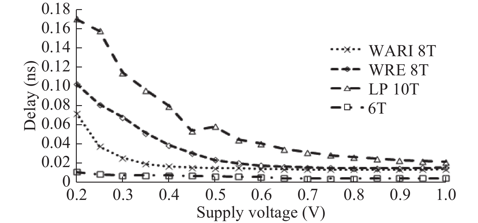
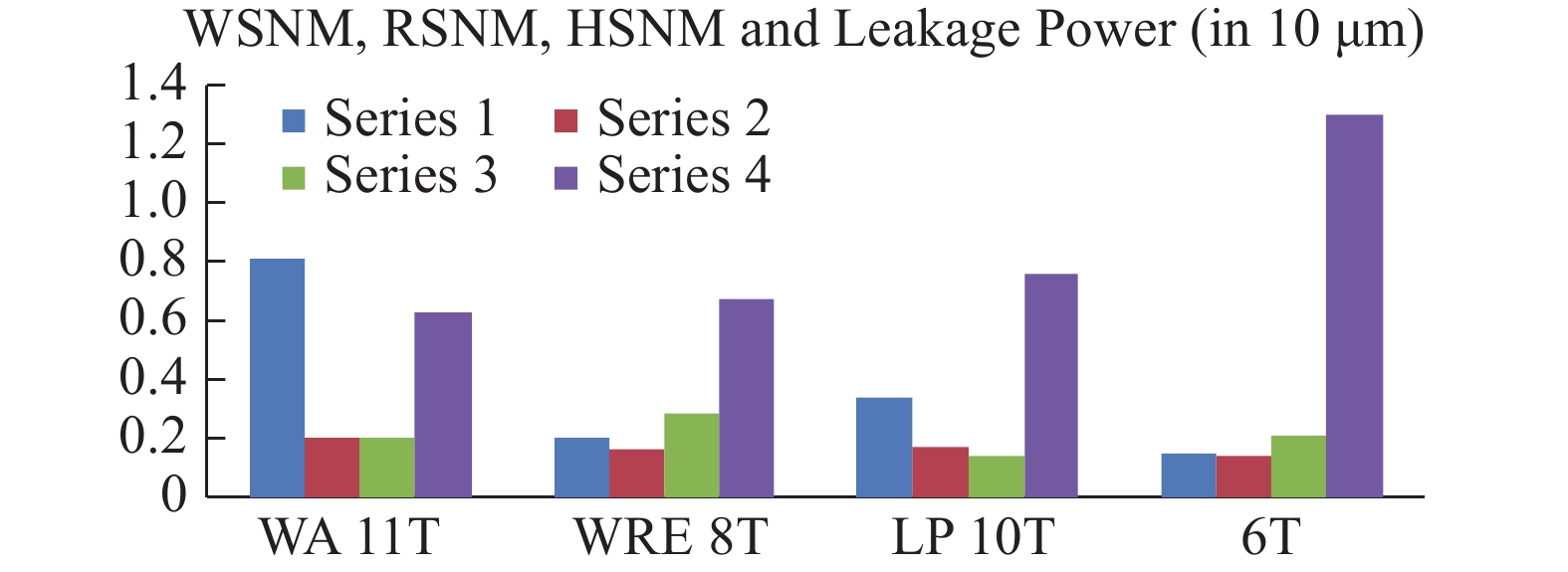


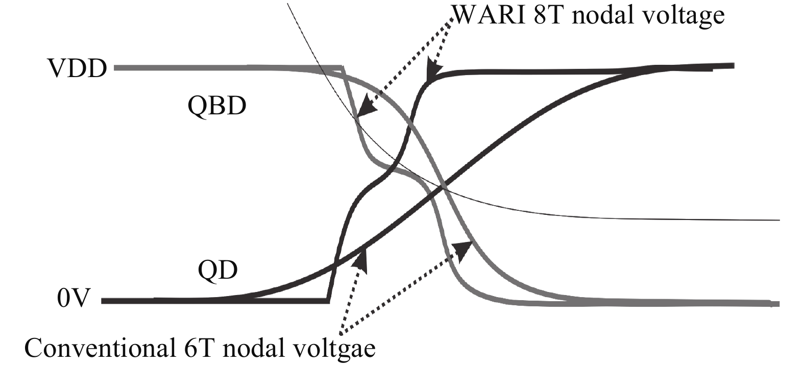
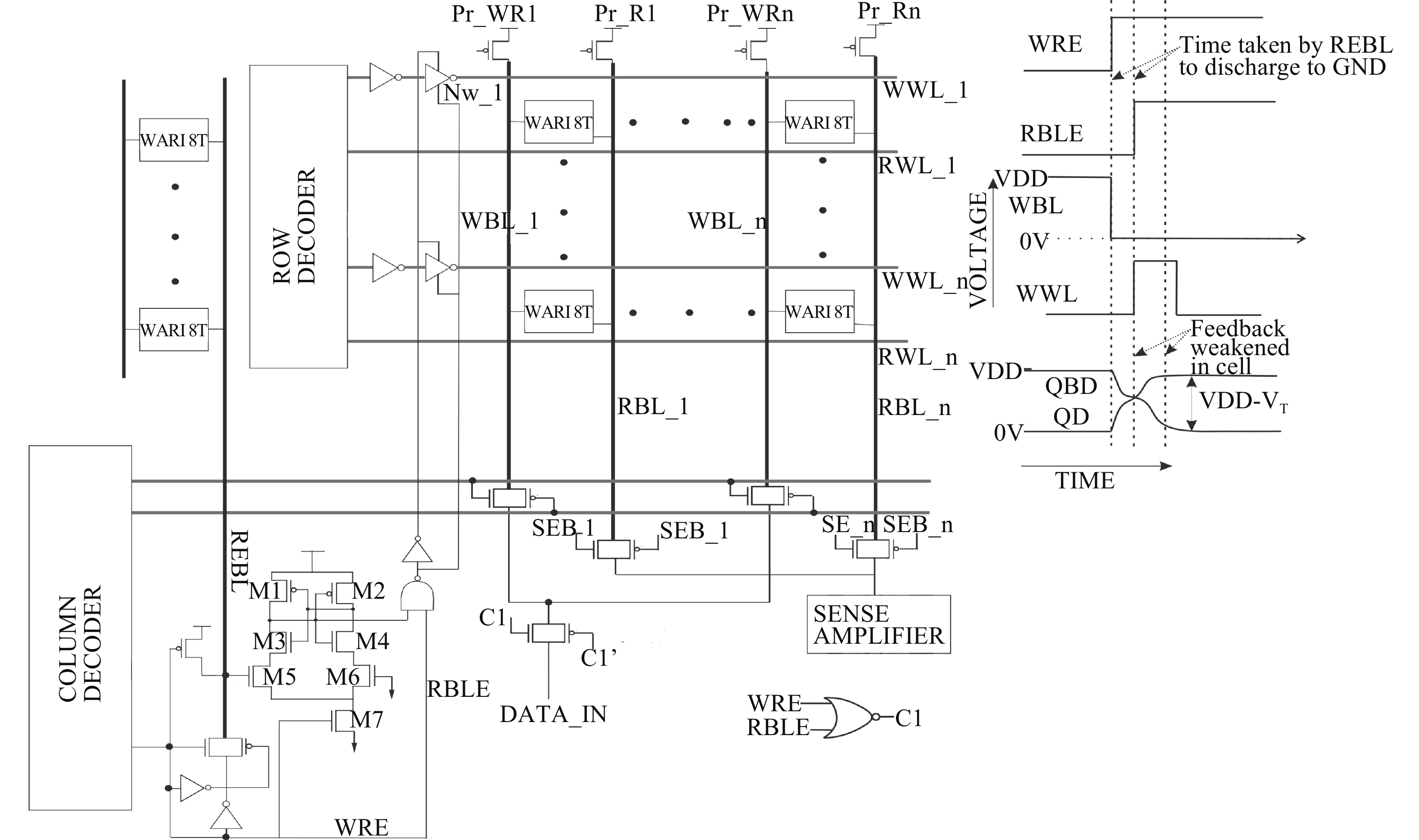
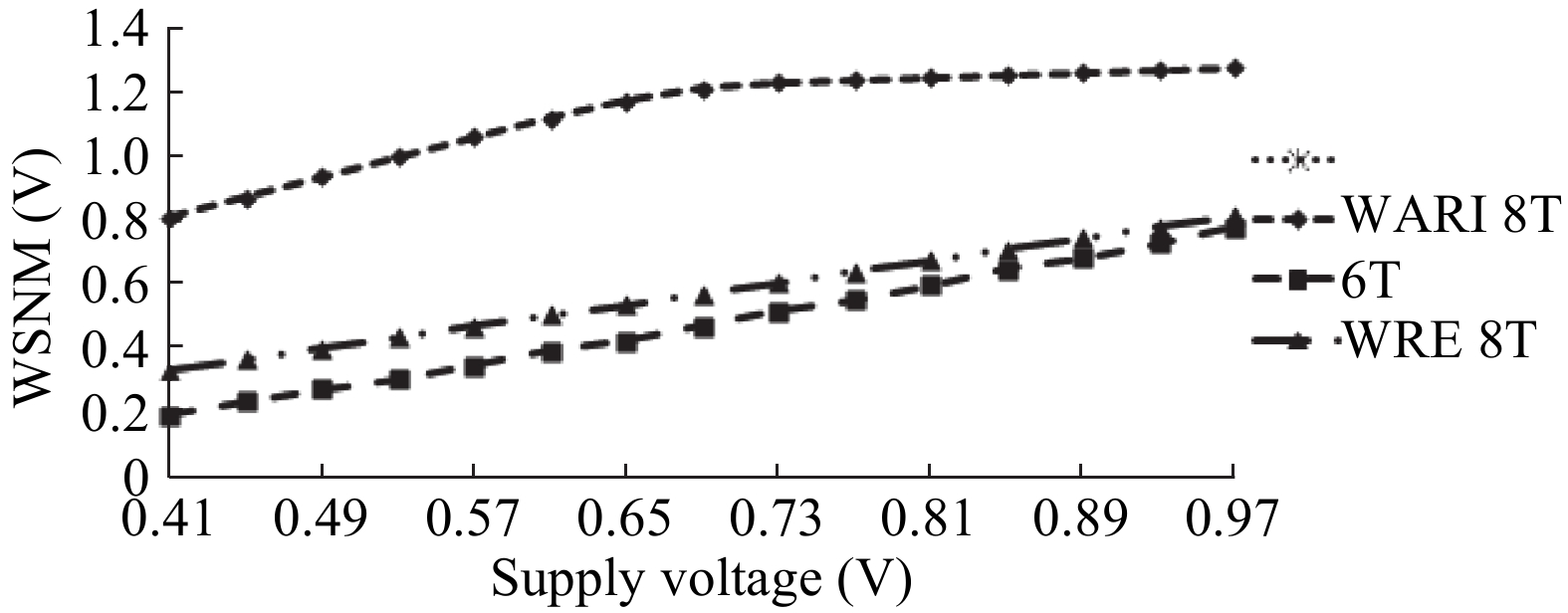
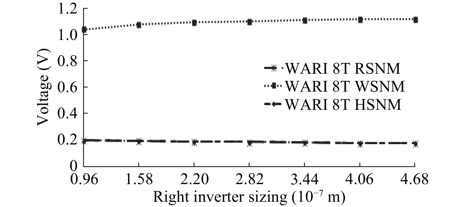
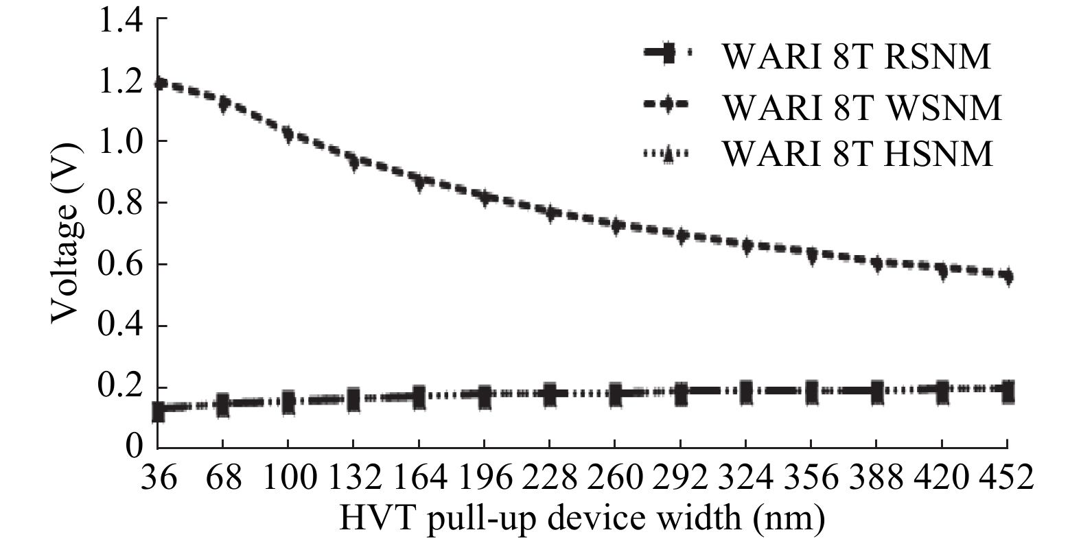
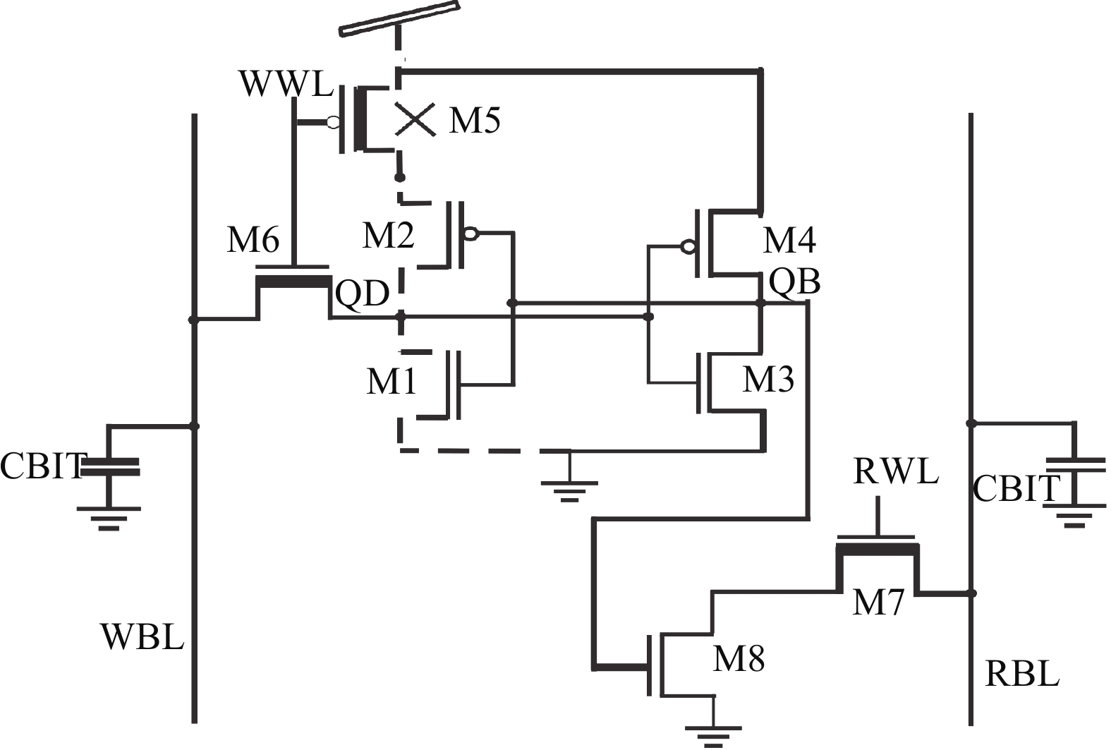
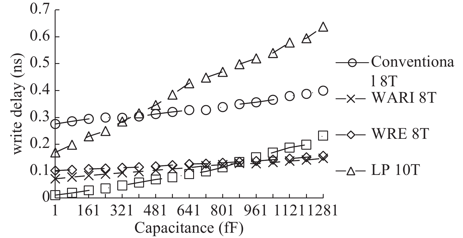
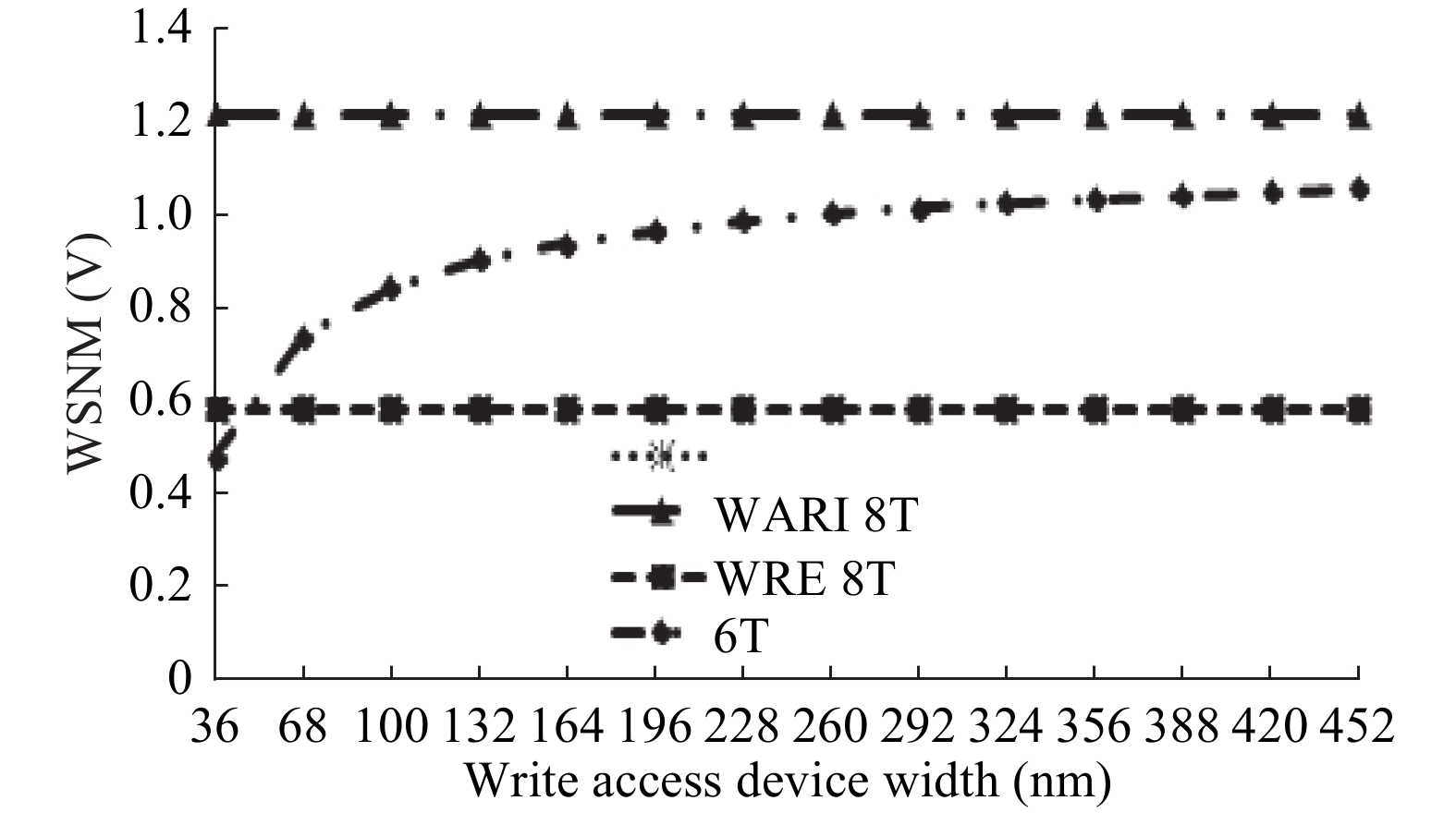
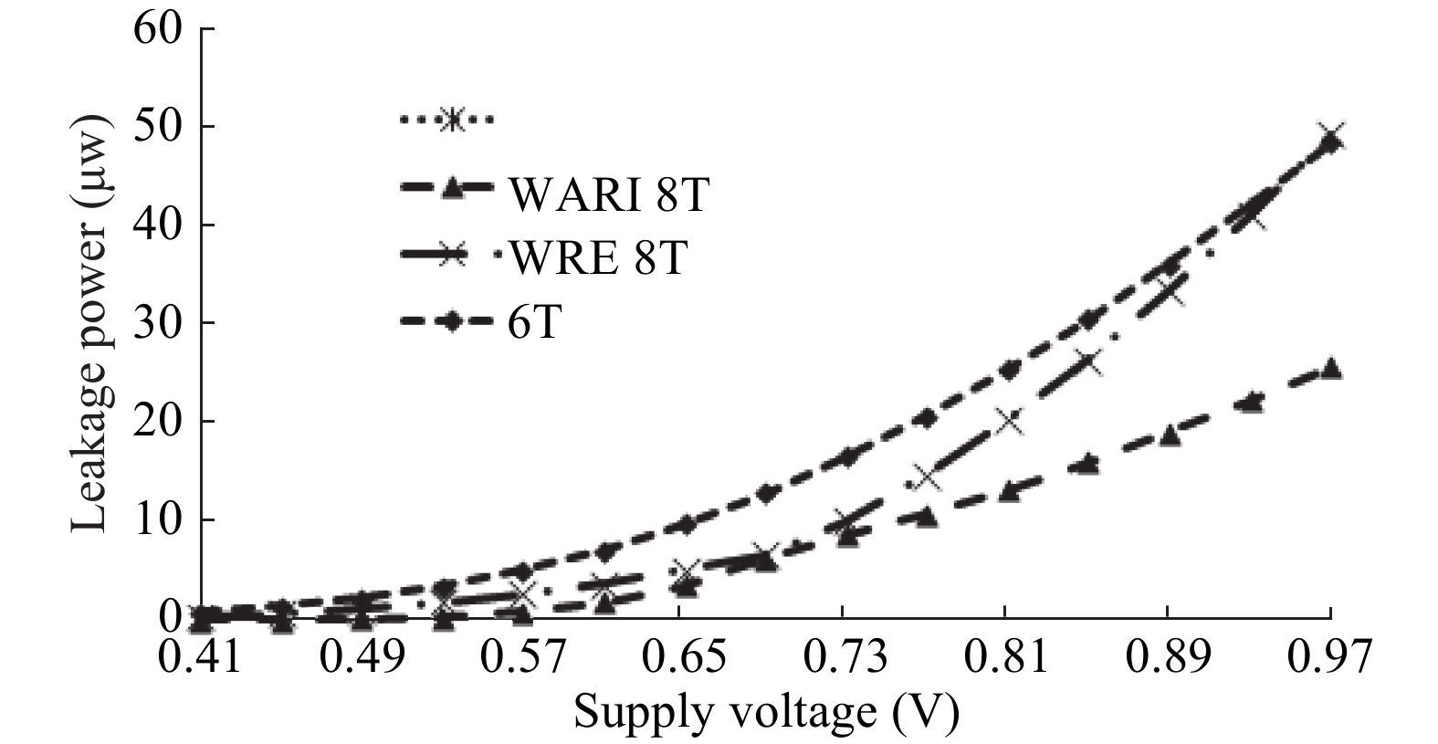
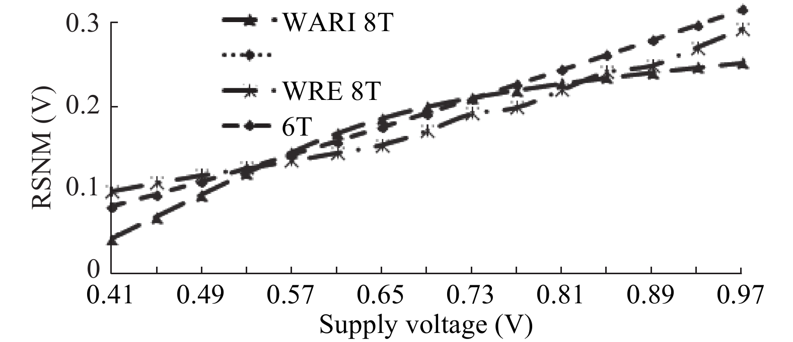
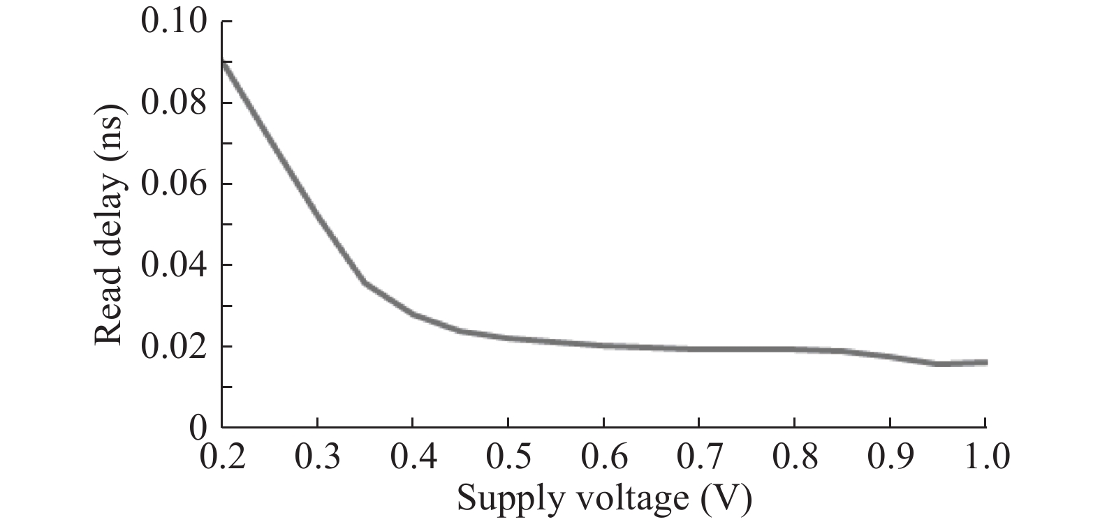
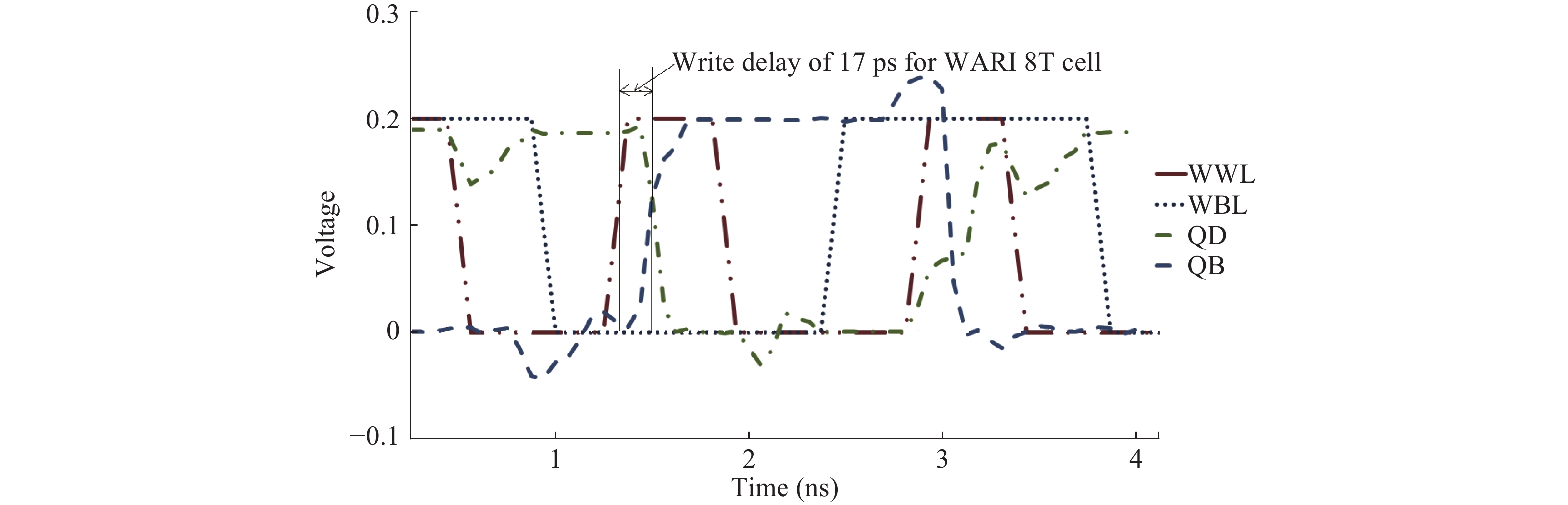
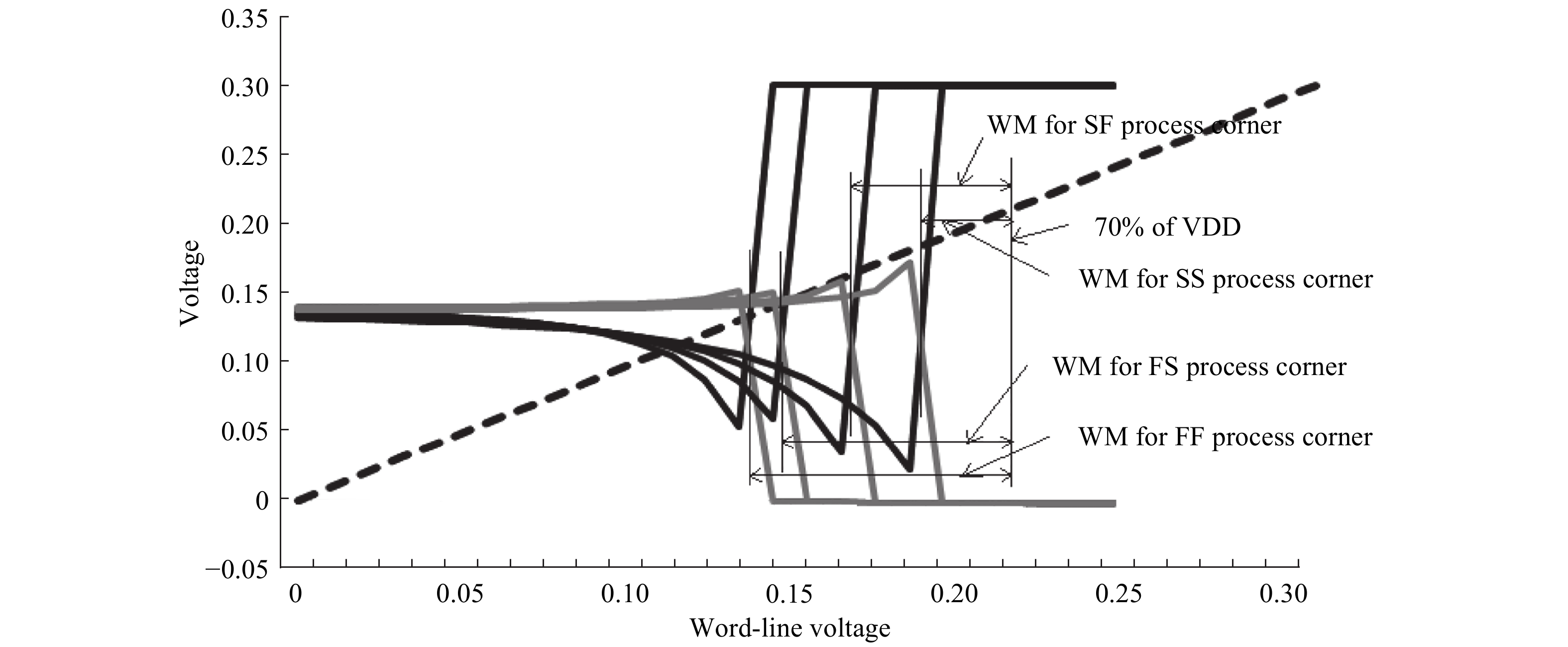
This paper presents a new dual Vt 8T SRAM cell having single bit-line read and write, in addition to Write Assist and Read Isolation (WARI). Also a faster write back scheme is proposed for the half selected cells. A high Vt device is used for interrupting the supply to one of the inverters for weakening the feedback loop for assisted write. The proposed cell provides an improved read static noise margin (RSNM) due to the bit-line isolation during the read. Static noise margins for data read (RSNM), write (WSNM), read delay, write delay, data retention voltage (DRV), leakage and average powers have been calculated. The proposed cell was found to operate properly at a supply voltage as small as 0.41 V. A new write back scheme has been suggested for half-selected cells, which uses a single NMOS access device and provides reduced delay, pulse timing hardware requirements and power consumption. The proposed new WARI 8T cell shows better performance in terms of easier write, improved read noise margin, reduced leakage power, and less delay as compared to the existing schemes that have been available so far. It was also observed that with proper adjustment of the cell ratio the supply voltage can further be reduced to 0.2 V.


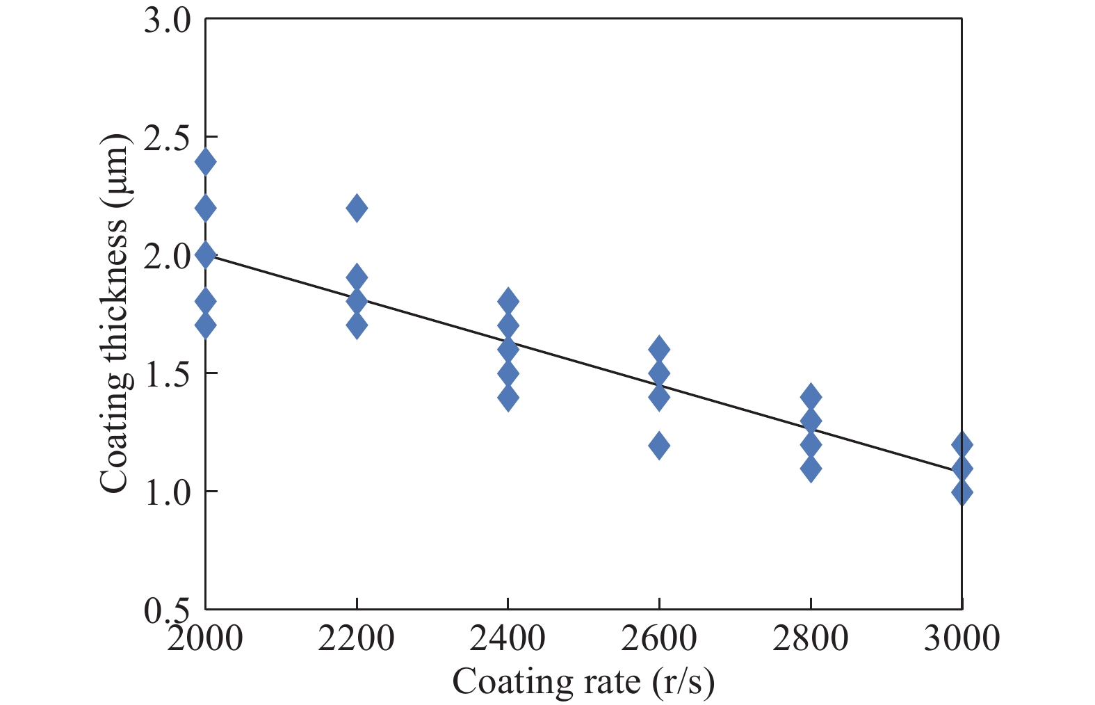
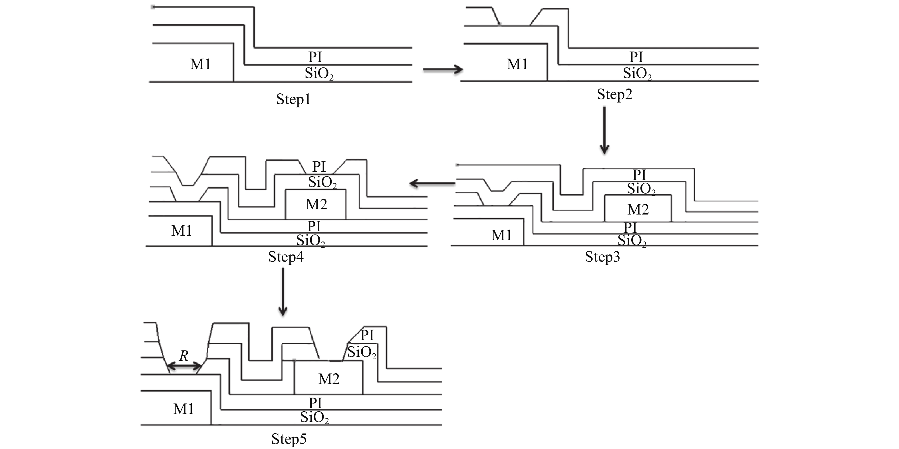
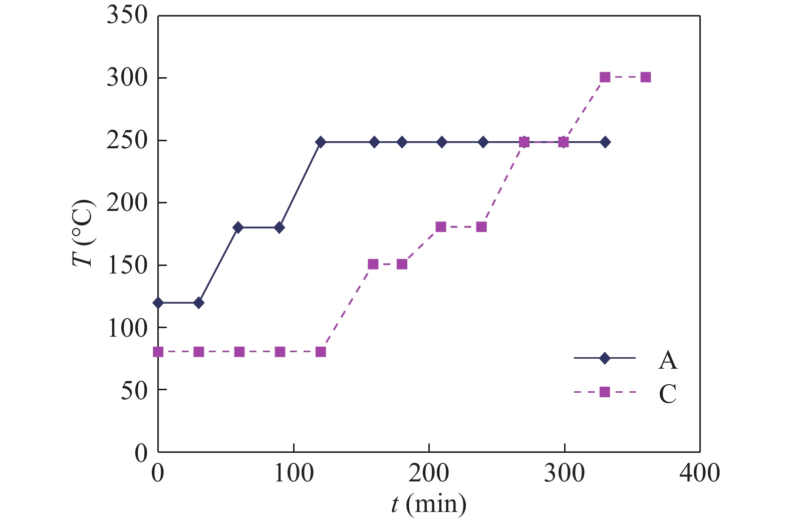
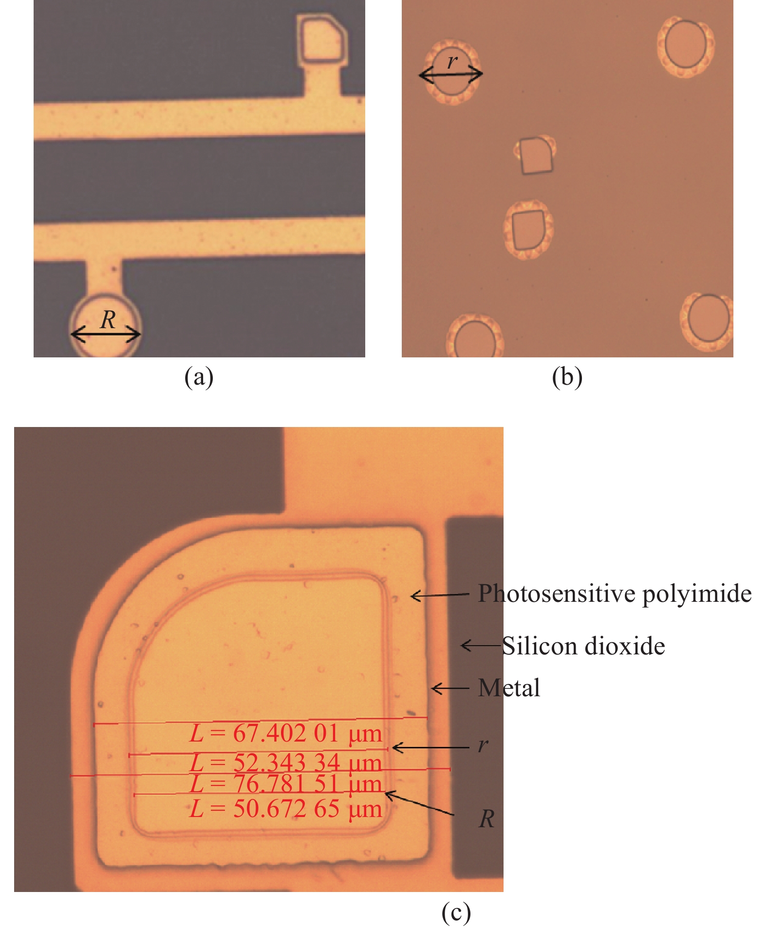
Positive type photosensitive polyimide is used as the modification layer in the thin film transistors production process. The photosensitive polyimide is not only used as the second insulating layer, it can also be used instead of a mask because of the photosensitivity. A suitable curing condition can help photosensitive polyimide form the high performance polyimide with orderly texture inside, and the performance of imidization depends on the precise control of temperature, time, and heat control during the curing process. Therefore, experiments of different stepped up heating tests are made, and the ability of protecting silicon dioxide is analyzed.
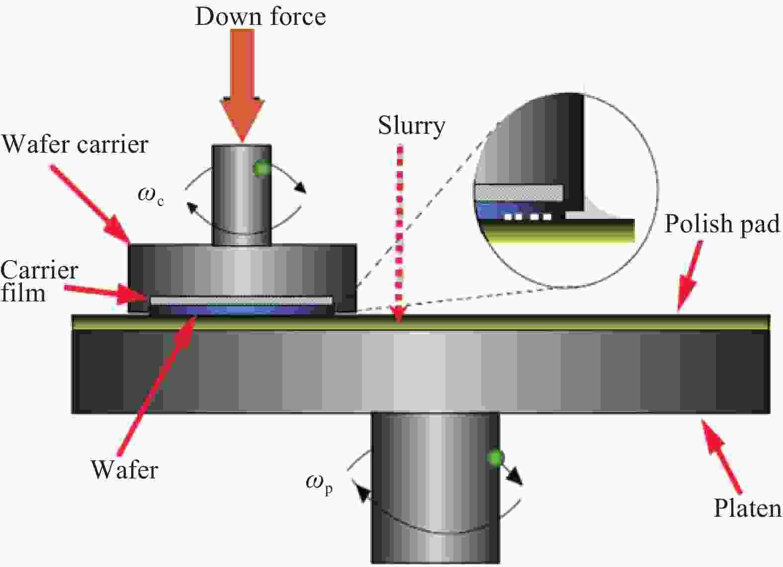
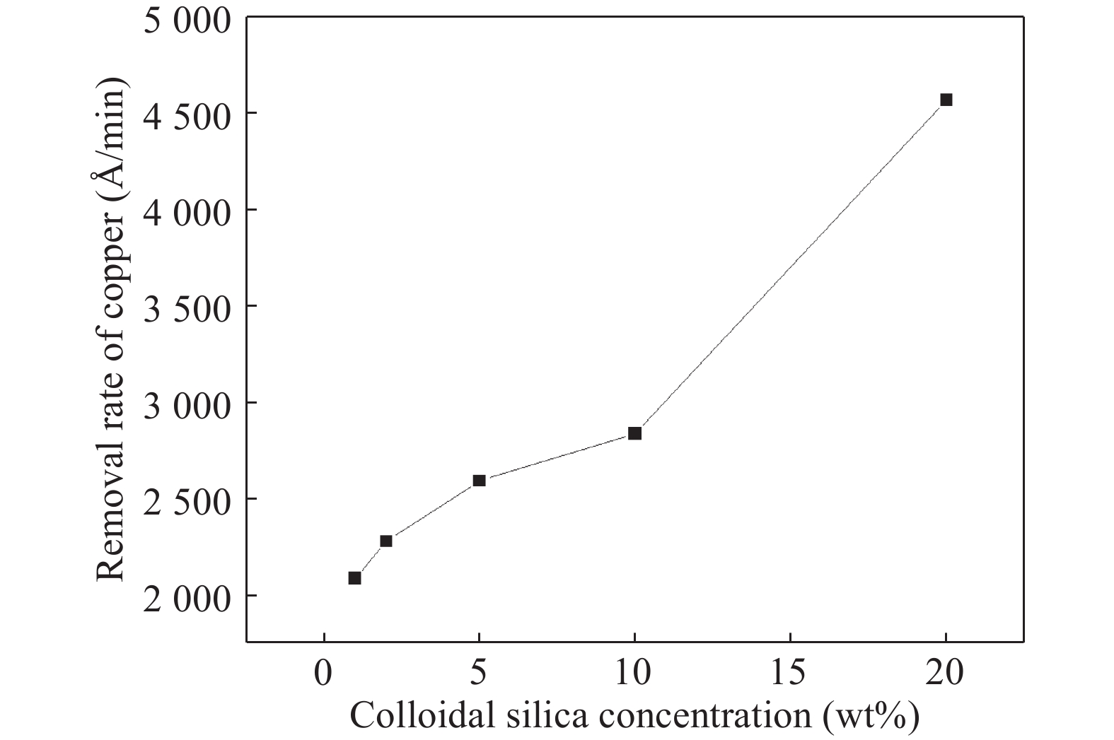
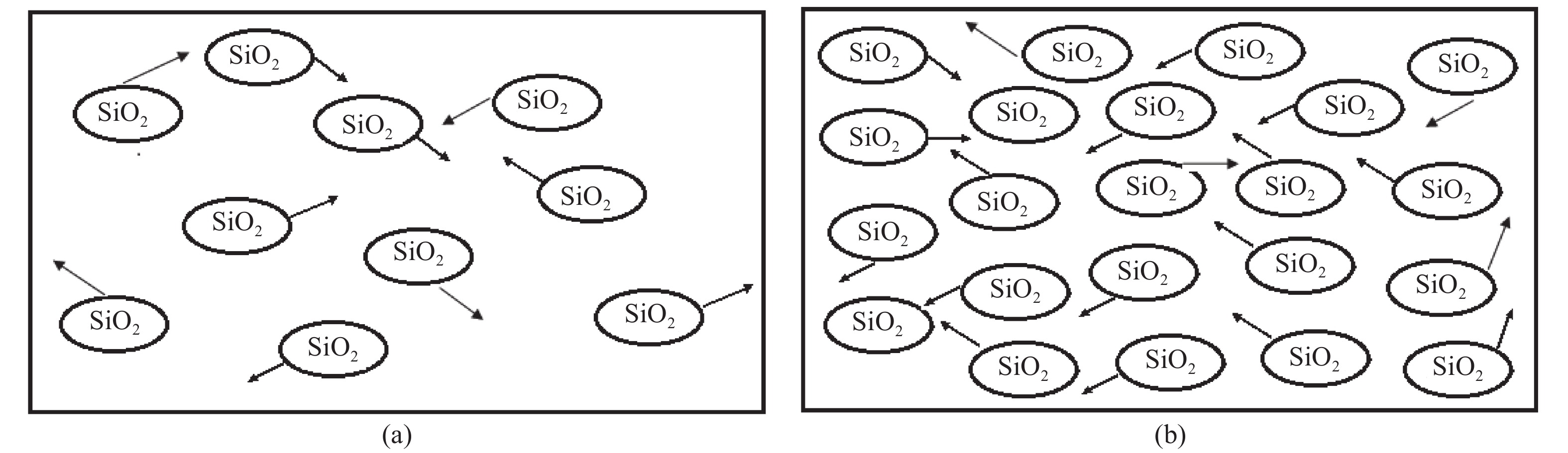
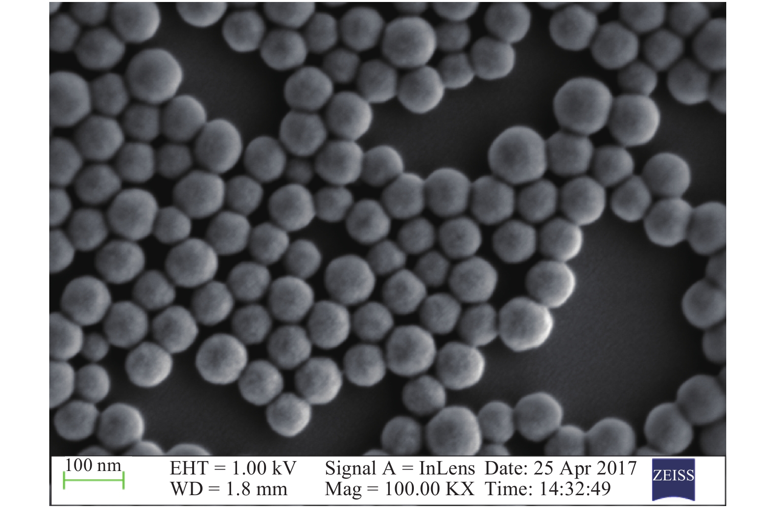
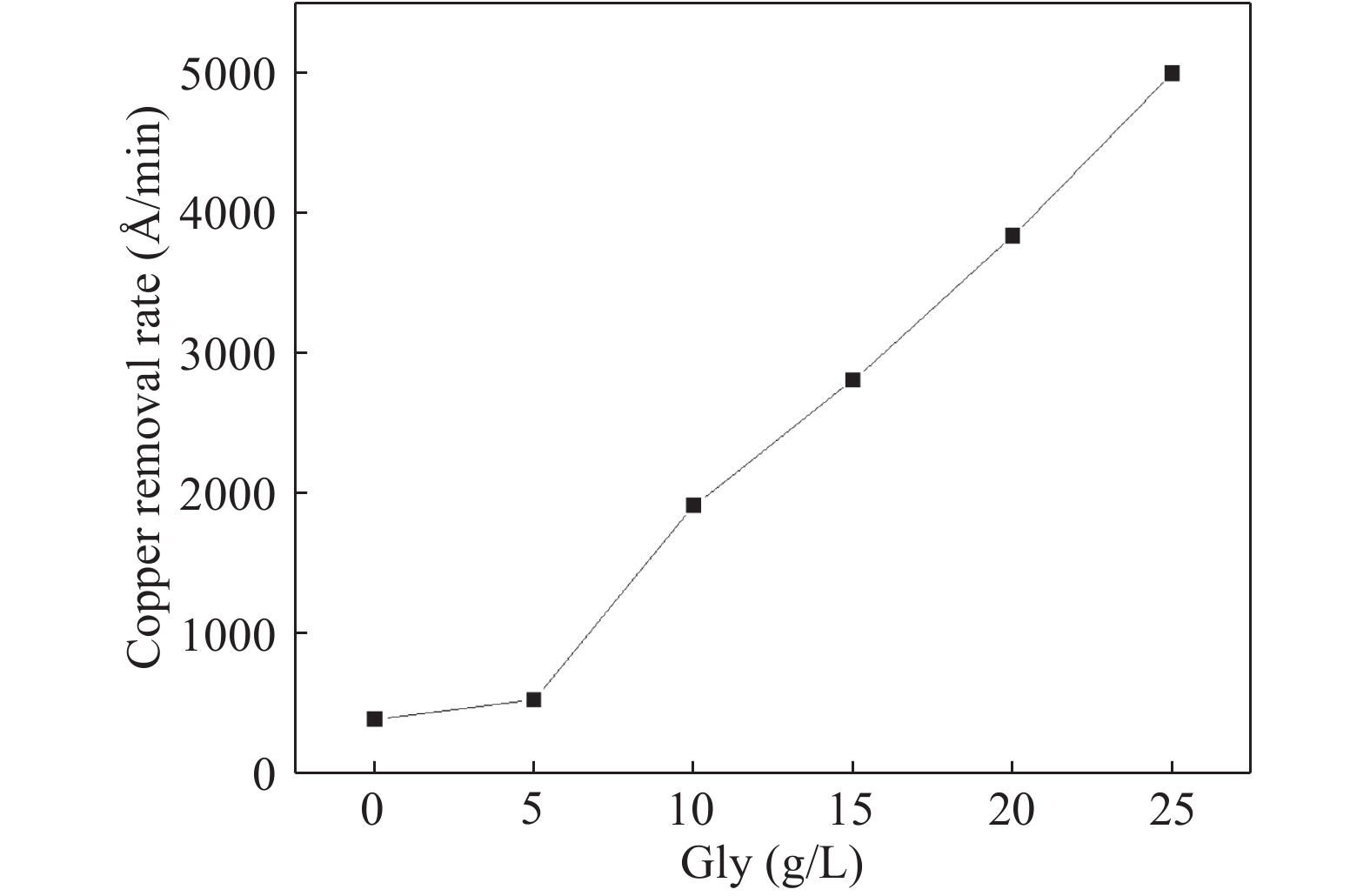
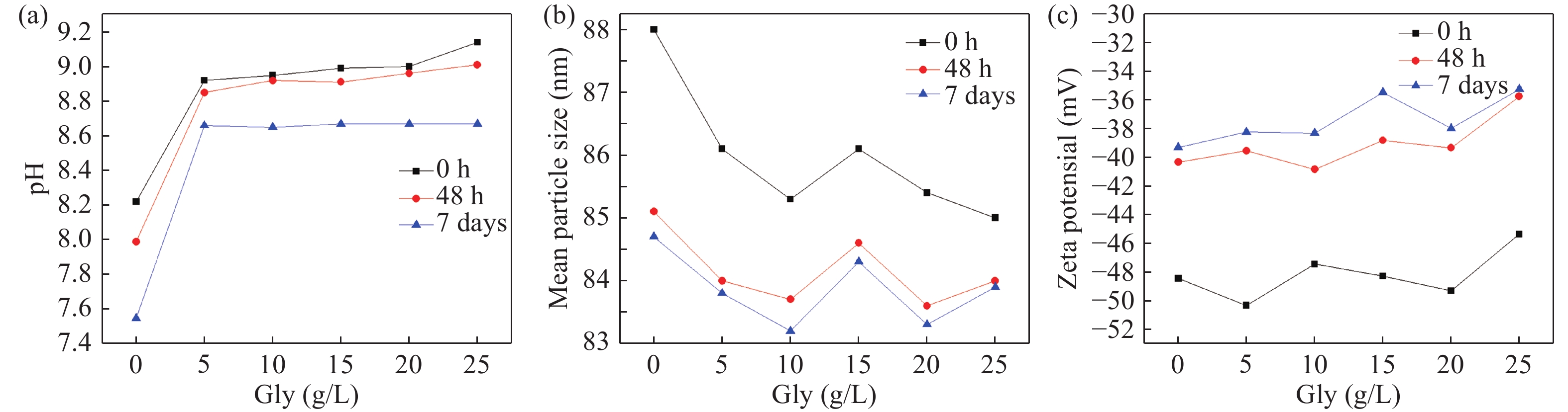
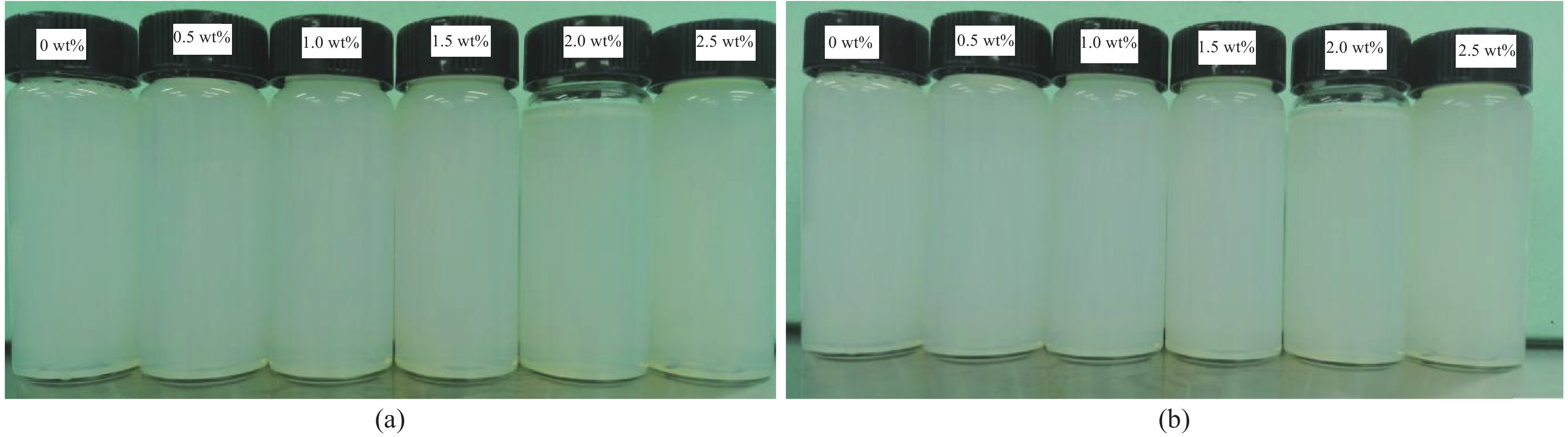
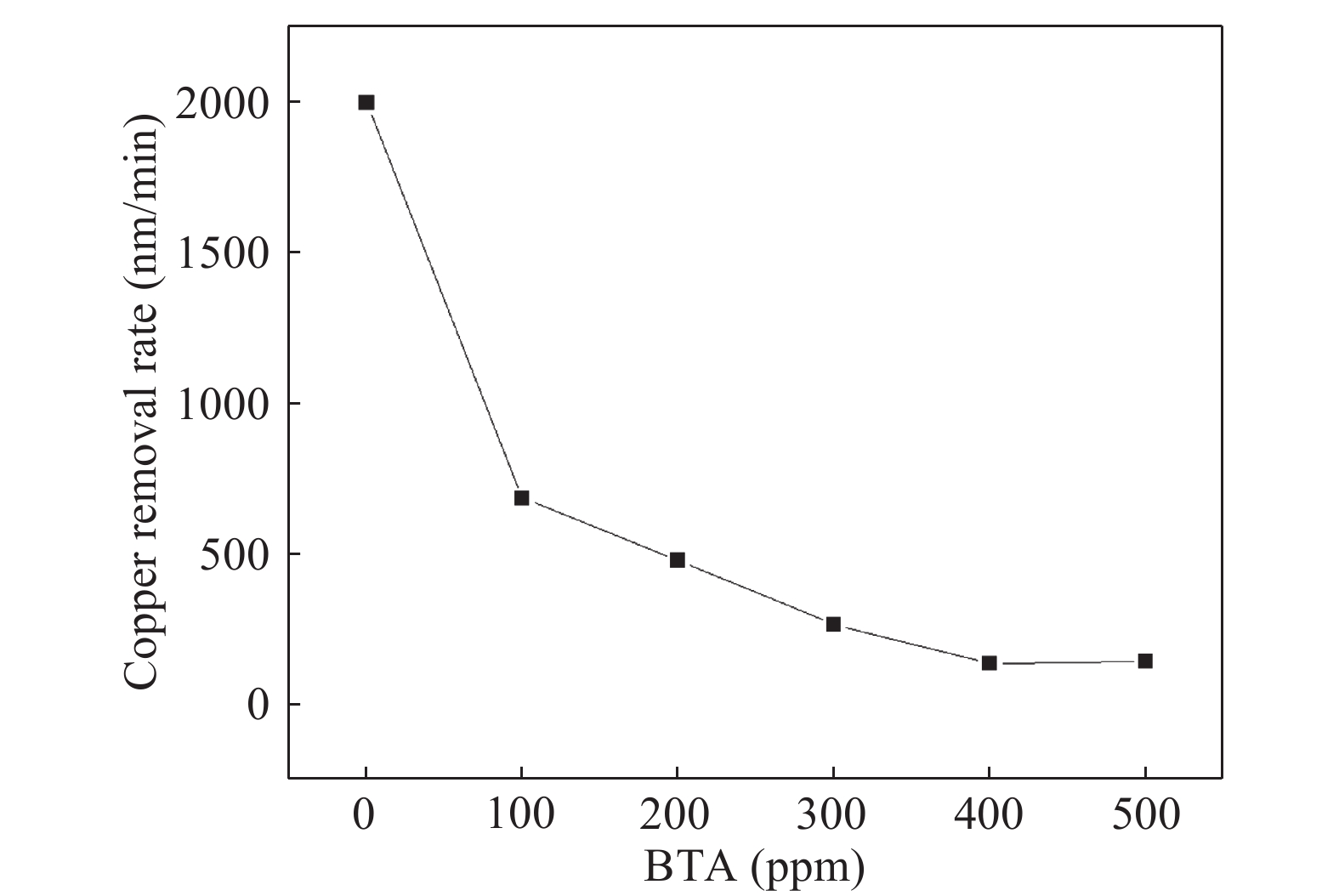
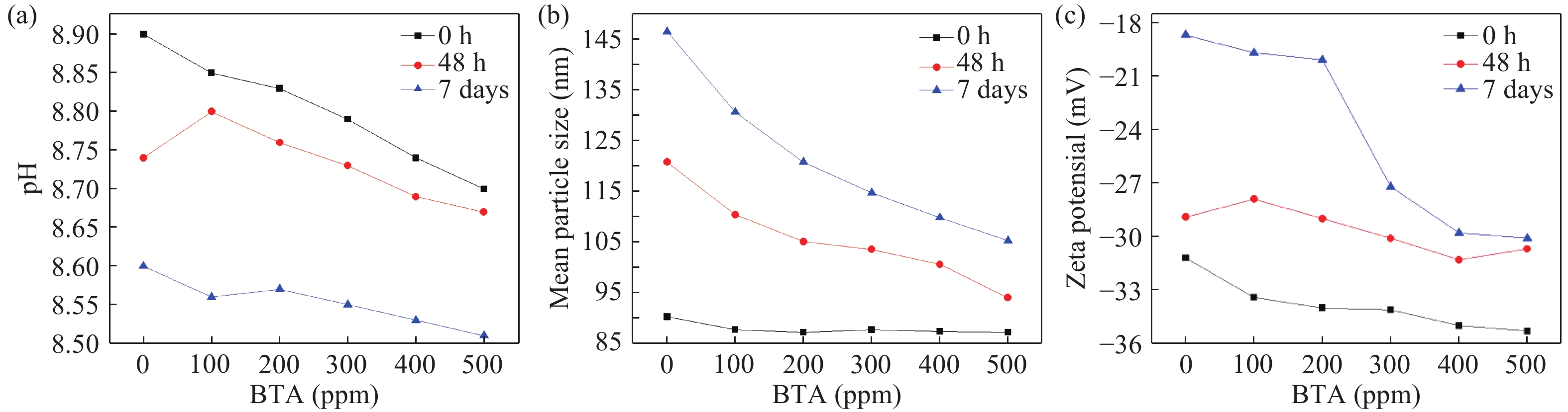
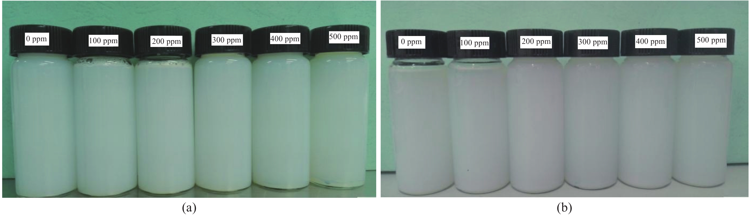
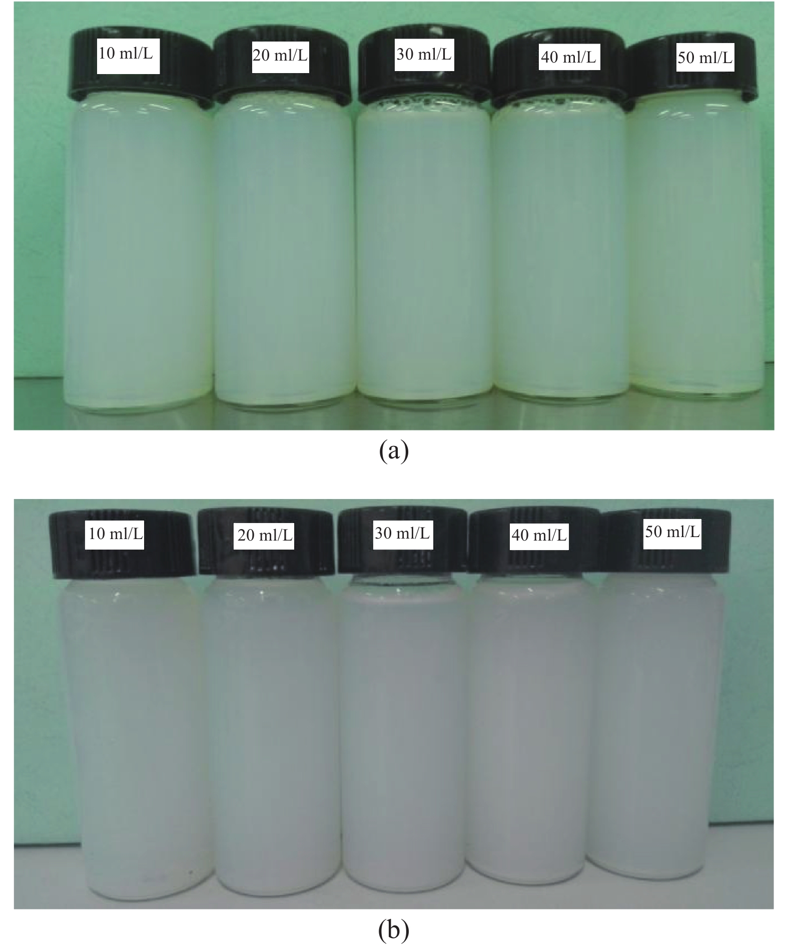
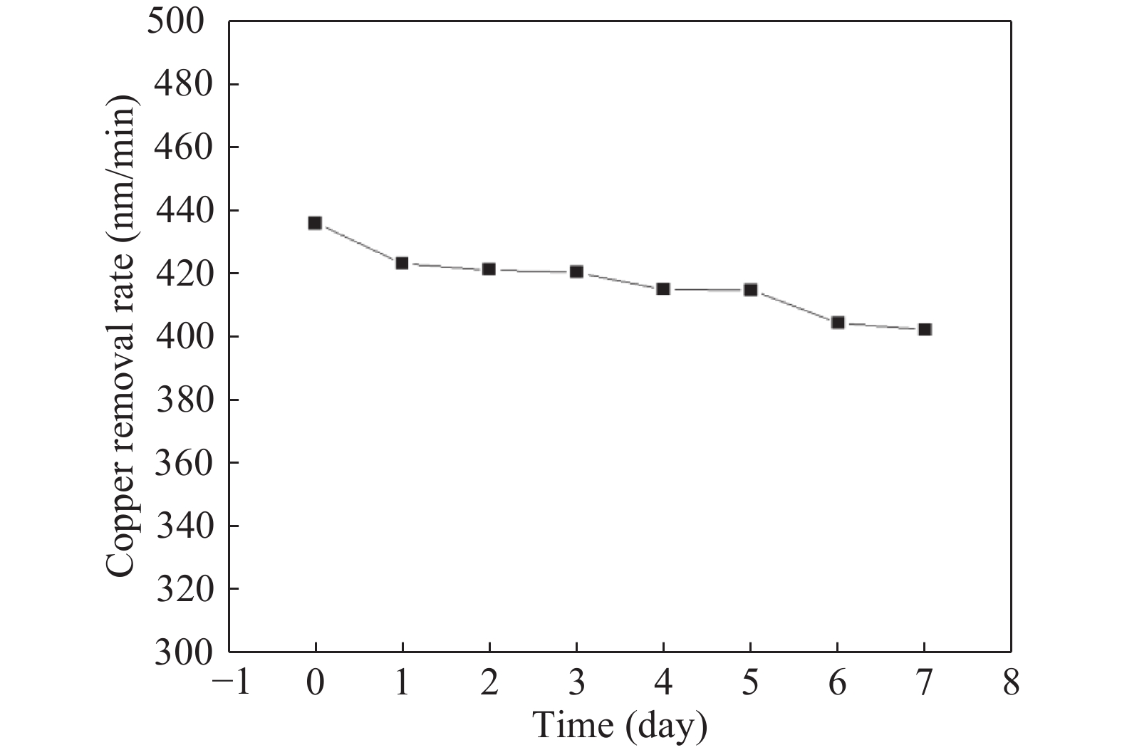
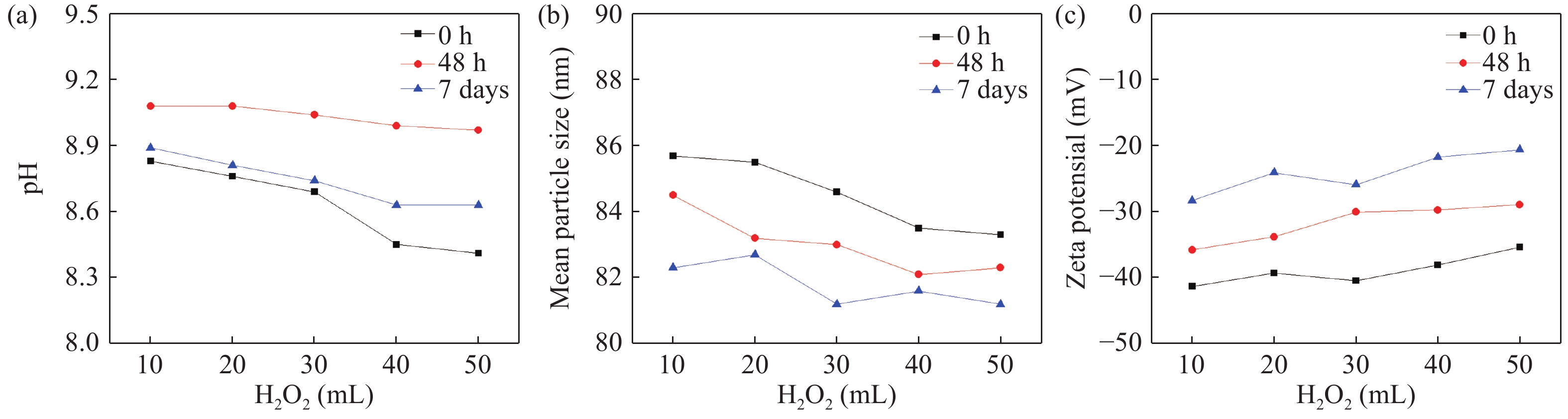
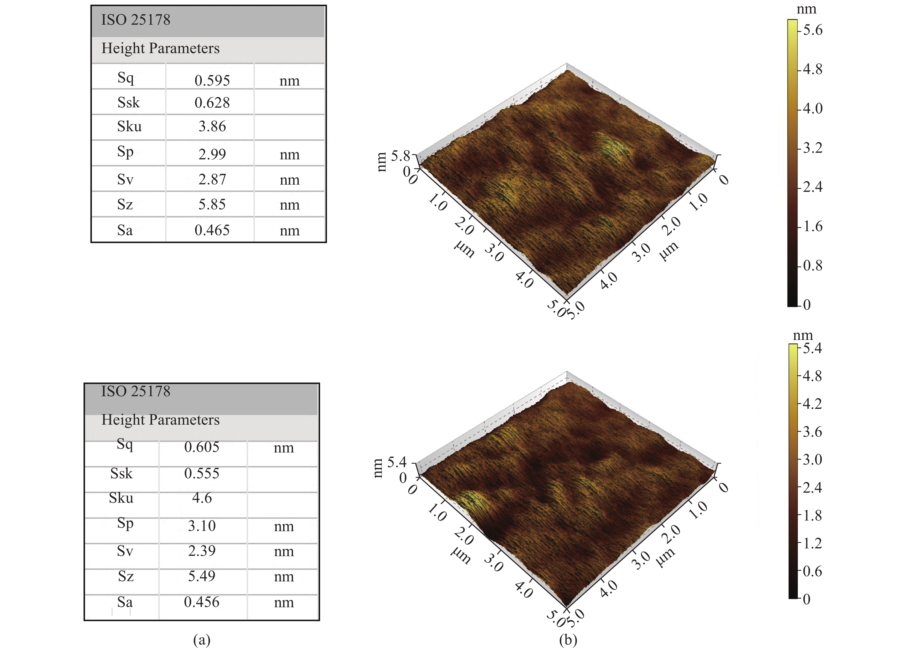
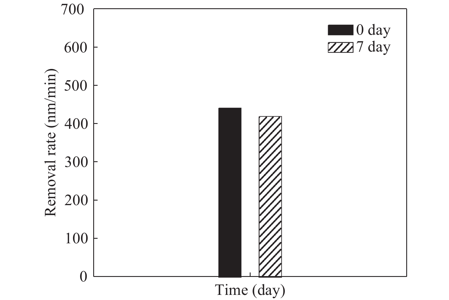
Chemical mechanical polishing (CMP) is one of the important machining procedures of multilayered copper interconnection for GLSI, meanwhile polishing slurry is a critical factor for realizing the high polishing performance such as high planarization efficiency, low surface roughness. The effect of slurry components such as abrasive (colloidal silica), complexing agent (glycine), inhibitor (BTA) and oxidizing agent (H2O2) on the stability of the novel weakly alkaline slurry of copper interconnection CMP for GLSI was investigated in this paper. First, the synergistic and competitive relationship of them in a peroxide-based weakly alkaline slurry during the copper CMP process was studied and the stability mechanism was put forward. Then 1 wt% colloidal silica, 2.5 wt% glycine, 200 ppm BTA, 20 mL/L H2O2 had been selected as the appropriate concentration to prepare copper slurry, and using such slurry the copper blanket wafer was polished. From the variations of copper removal rate, root-mean square roughness (Sq) value with the setting time, it indicates that the working-life of the novel weakly alkaline slurry can reach more than 7 days, which satisfies the requirement of microelectronics further development.


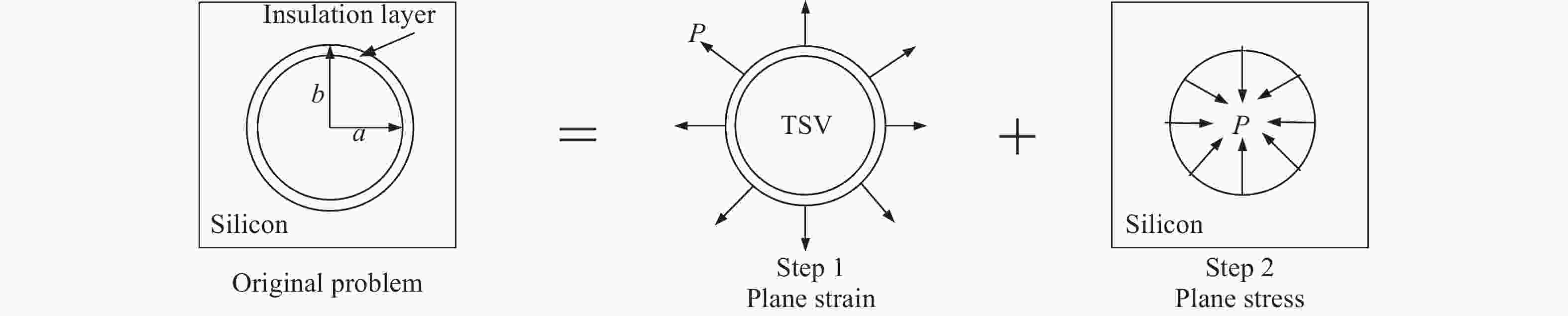
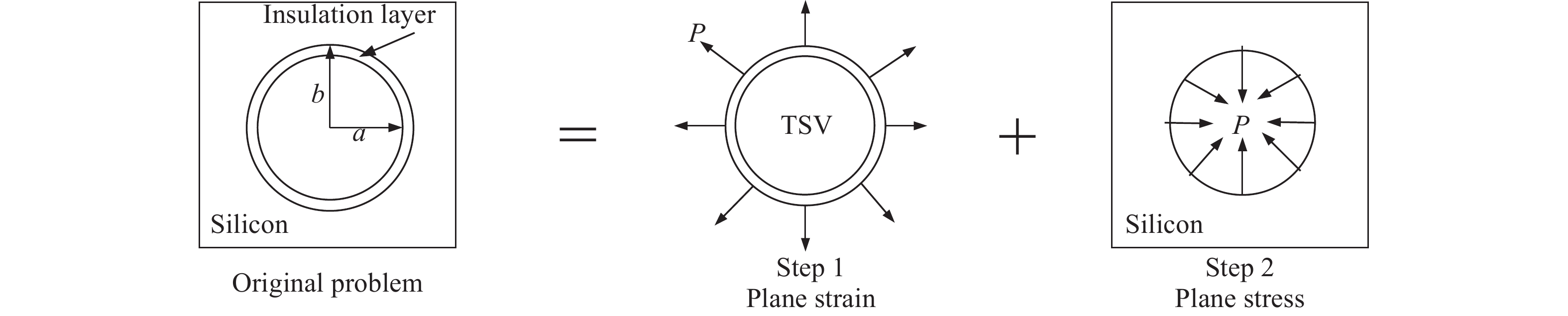
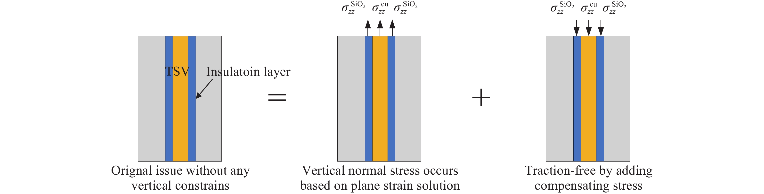
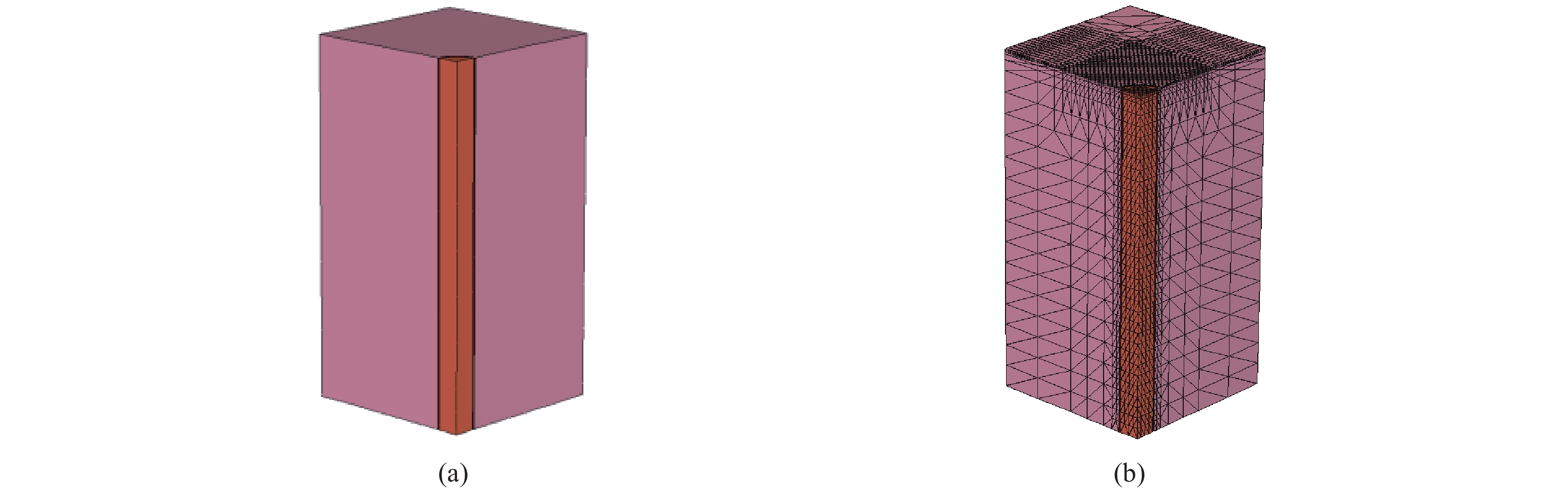
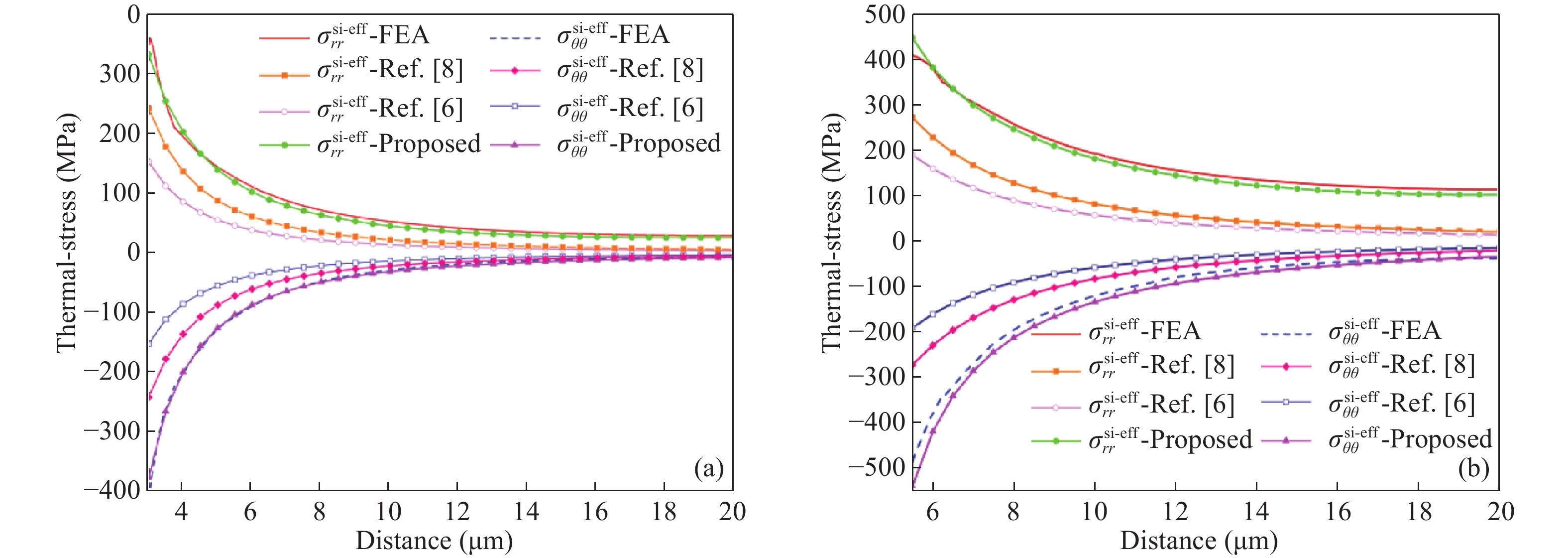
A two-dimensional thermal-stress model of through-silicon via (TSV) is proposed considering the anisotropic elastic property of the silicon substrate. By using the complex variable approach, the distribution of thermal-stress in the substrate can be characterized more accurately. TCAD 3-D simulations are used to verify the model accuracy and well agree with analytical results (< ±5%). The proposed thermal-stress model can be integrated into stress-driven design flow for 3-D IC , leading to the more accurate timing analysis considering the thermal-stress effect.