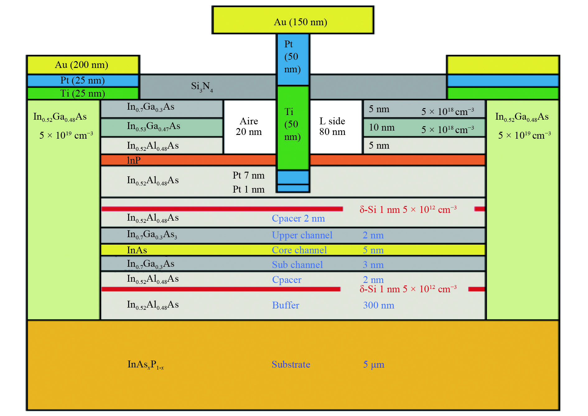
Fig. 1.
(Color online) Structure of simulated InAsP-Based HEMT.
SEMICONDUCTOR DEVICES
S. Derrouiche1, , B. Bouazza1 and C. Sayah2
Corresponding author: S. Derrouiche, derrouiche.soufiane@gmail.com
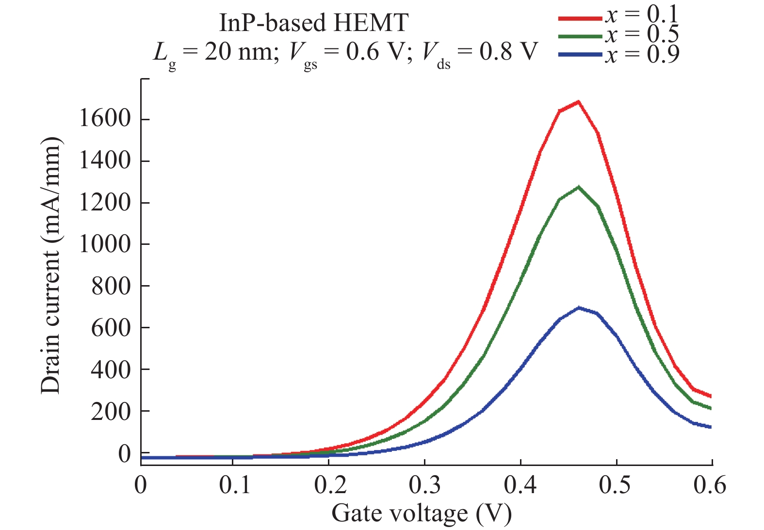
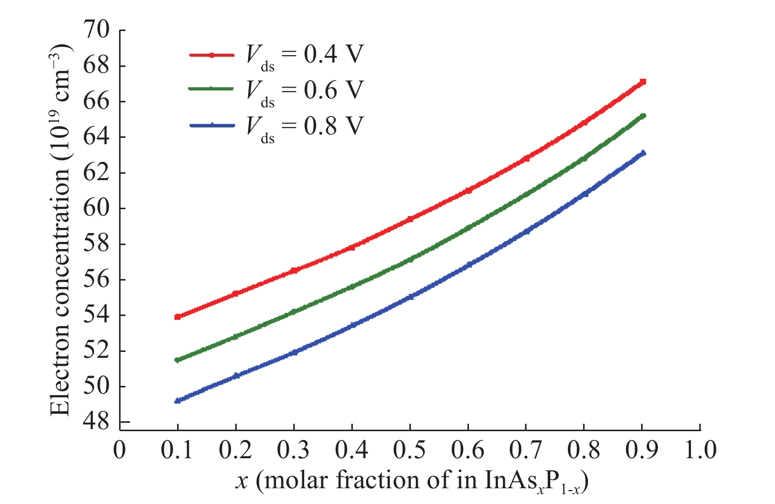
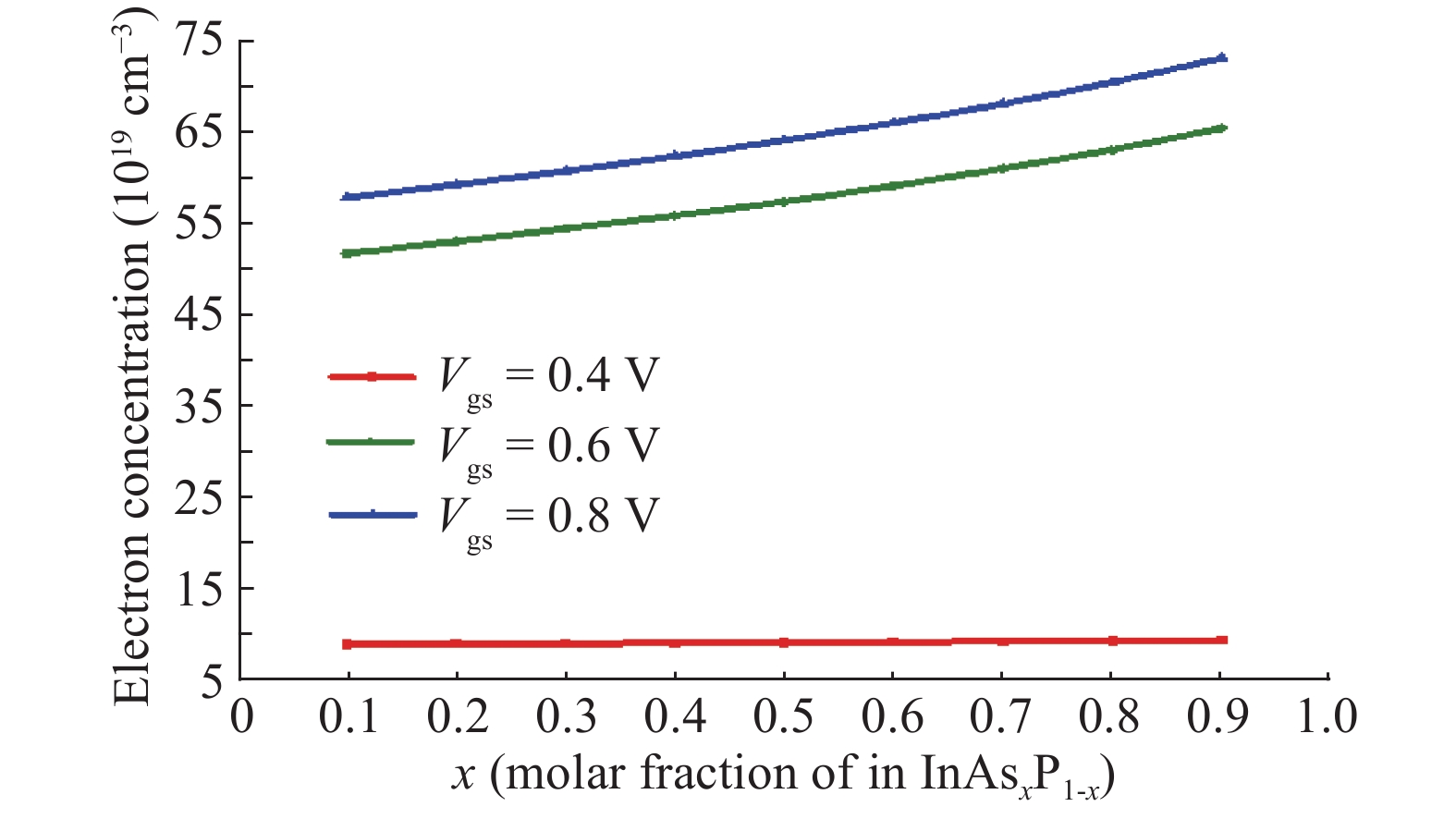
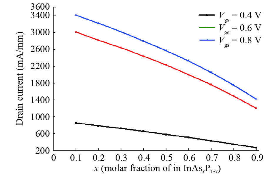
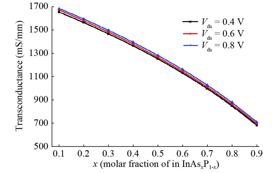
Abstract: We present the drain current modulation for an HEMT using the TCAD SILVACO simulation tool with a drift–diffusion model at ambient temperature. The obtained results show that the decreases of substrate energies induce the decreasing of the obtained drain current similarly to the transconductance, which described the device due to increasing the transferred electrons concentration towards the substrate region, consequently to increase the molar fraction where the concentration of transferred electrons increases from 49 × 1019 to 65 × 1019 cm−3 when the molar fraction increases from 0.1 to 0.9. On the other hand, the decrease of molar fraction from 0.9 to 0.1 induces the increasing of drain current by 63%, where it increases from 1.1 mA/mm to 3 mA/mm at Vgs = 0.6 V and Vds = 1 V. This fact leads to ensuring the possibility of using the obtained results of this work related to drain current for producing performances devices that brings together the AC characteristics of HEMT with a weak drain current, which is important in the bioengineering domain.
Key words: high electron mobility transistors (HEMT), electron concentration, drain current modulation, electron injection, bio-engineering
| [1] |
Radisic V, Leong K M K H , Scott D W, et al Sub-millimeter wave InP technologies and integration techniques. Sub-millimeter wave InP technologies and integration techniques. IEEE MTT-S International Microwave Symposium (IMS), 2015 doi: 10.1109/MWSYM.2015.7167151
|
| [2] |
Deal W R, Leong K, Zamora A, et al. Recent progress in scaling InP HEMT TMIC technology to 850 GHz. 2014 IEEE MTT-S International Microwave Dig, 2014 doi: 10.1109/MWSYM.2014.6848588
|
| [3] |
Leong M K H K, Mei X, Yoshida W, et al. A 0.85 THz low noise amplifier using InP HEMT transistors. IEEE Microwave Wireless Compon Lett, 2015, 25(6): 397 doi: 10.1109/LMWC.2015.2421336
|
| [4] |
Hacker J, Urtega M, Seo M, et al. InP HBT amplifier MMICs operating to 0.67 THz. IEEE MTT-S International Microwave Dig, 2013: 1
|
| [5] |
Reed T B, Griffith Z, Rowell P, et al. A 180 mW InP HBT power amplifier MMIC at 214. IEEE Compound Semiconductor Integrated Circuit Symposium, 2013: 1 doi: 10.1109/CSICS.2013.6659187
|
| [6] |
Radisic V, Scott D W, Cavus A, et al. 220-GHz high-efficiency InP HBT power amplifiers. IEEE Trans Microwave Theory Tech, 2014, 62: 3001 doi: 10.1109/TMTT.2014.23622133
|
| [7] |
Radisic V, Scott D W, Monier C, et al. InP HBT transferred substrate amplifiers operating to 600 GHz, in IEEE MTT-S International Microwave Dig, 2015, doi10.1109/MWSYM.2015. 7166750.
|
| [8] |
Shin S H, Kim T W, Song J I, et al. Buried-Pt gate InP/In0.52Al0.48As/In0.7Ga0.3As pseudomorphic HEMTs. Solid-State Electron, 2011(62): 106 doi: 10.1016/j.sse.2011.02.002
|
| [9] |
Kim D H, Brar B, del-Alamo J A. fT = 688 GHz and fmax = 800 GHz in Lg = 40 nm In0.7Ga0.3As MHEMTs with gm_max > 2.7 mS/μm. Proceedings of IEDM Technical Digest, 2011: 319
|
| [10] |
Wang L D, Ding P, Su Y B, et al. 100-nm T-gate InAlAs/InGaAs InP-based HEMTs with fT = 249 GHz and fmax = 415 GHz. Chin Phys B, 2014, 23(3): 038501 doi: 10.1088/1674-1056/23/3/038501
|
| [11] |
Saravana K R, Mohanbabu A, Mohankuma N, et al. Simulation of InGaAs sub-channel DG-HEMTs for analog / RF applications. Int J Electron, 2017, 105(3): 446 doi: 10.1080/00207217.2017.1376354
|
| [12] |
Chatterjee S. fT = 152 GHz and fMAX = 196 GHz in a 130 nm gate InP HEMT. Int J Electron Commun Eng, 2017, 10(1): 1
|
| [13] |
Galiev G B, Vasiliev A L, Imamov R M, et al. Structural and electrical properties of InAlAs/InGaAs/InAlAs HEMT heterostructures on InP substrates with InAs inserts in quantum well. Crystallography Reports, 2014, 59(6): 900 doi: 10.1134/S1063774515030128
|
| [14] |
Ajayan J, Nirmal D. 20 nm high performance enhancement mode InP HEMT with heavily doped S/D regions for future THz applications. Superlattices Microstruct, 2016, 100: 526 doi: 10.1016/j.epmi.2016.10.011
|
| [15] |
Pinto M R, Rafferty C S, Dutton R W. PISCES2- Poisson and continuity equation solver. Stanford Electronics Laboratory Technical Report, Stanford University, 1984
|


Article views: 3277 Times PDF downloads: 60 Times Cited by: 0 Times
Received: 20 March 2018 Revised: 03 May 2018 Online: Uncorrected proof: 28 June 2018Published: 01 November 2018
| Citation: |
S. Derrouiche, B. Bouazza, C. Sayah. Modulation of drain current as a function of energies substrate for InP HEMT devices[J]. Journal of Semiconductors, 2018, 39(11): 114002. doi: 10.1088/1674-4926/39/11/114002
S Derrouiche, B Bouazza, C Sayah, Modulation of drain current as a function of energies substrate for InP HEMT devices[J]. J. Semicond., 2018, 39(11): 114002. doi: 10.1088/1674-4926/39/11/114002.
Export: BibTex EndNote

|
| [1] |
Radisic V, Leong K M K H , Scott D W, et al Sub-millimeter wave InP technologies and integration techniques. Sub-millimeter wave InP technologies and integration techniques. IEEE MTT-S International Microwave Symposium (IMS), 2015 doi: 10.1109/MWSYM.2015.7167151
|
| [2] |
Deal W R, Leong K, Zamora A, et al. Recent progress in scaling InP HEMT TMIC technology to 850 GHz. 2014 IEEE MTT-S International Microwave Dig, 2014 doi: 10.1109/MWSYM.2014.6848588
|
| [3] |
Leong M K H K, Mei X, Yoshida W, et al. A 0.85 THz low noise amplifier using InP HEMT transistors. IEEE Microwave Wireless Compon Lett, 2015, 25(6): 397 doi: 10.1109/LMWC.2015.2421336
|
| [4] |
Hacker J, Urtega M, Seo M, et al. InP HBT amplifier MMICs operating to 0.67 THz. IEEE MTT-S International Microwave Dig, 2013: 1
|
| [5] |
Reed T B, Griffith Z, Rowell P, et al. A 180 mW InP HBT power amplifier MMIC at 214. IEEE Compound Semiconductor Integrated Circuit Symposium, 2013: 1 doi: 10.1109/CSICS.2013.6659187
|
| [6] |
Radisic V, Scott D W, Cavus A, et al. 220-GHz high-efficiency InP HBT power amplifiers. IEEE Trans Microwave Theory Tech, 2014, 62: 3001 doi: 10.1109/TMTT.2014.23622133
|
| [7] |
Radisic V, Scott D W, Monier C, et al. InP HBT transferred substrate amplifiers operating to 600 GHz, in IEEE MTT-S International Microwave Dig, 2015, doi10.1109/MWSYM.2015. 7166750.
|
| [8] |
Shin S H, Kim T W, Song J I, et al. Buried-Pt gate InP/In0.52Al0.48As/In0.7Ga0.3As pseudomorphic HEMTs. Solid-State Electron, 2011(62): 106 doi: 10.1016/j.sse.2011.02.002
|
| [9] |
Kim D H, Brar B, del-Alamo J A. fT = 688 GHz and fmax = 800 GHz in Lg = 40 nm In0.7Ga0.3As MHEMTs with gm_max > 2.7 mS/μm. Proceedings of IEDM Technical Digest, 2011: 319
|
| [10] |
Wang L D, Ding P, Su Y B, et al. 100-nm T-gate InAlAs/InGaAs InP-based HEMTs with fT = 249 GHz and fmax = 415 GHz. Chin Phys B, 2014, 23(3): 038501 doi: 10.1088/1674-1056/23/3/038501
|
| [11] |
Saravana K R, Mohanbabu A, Mohankuma N, et al. Simulation of InGaAs sub-channel DG-HEMTs for analog / RF applications. Int J Electron, 2017, 105(3): 446 doi: 10.1080/00207217.2017.1376354
|
| [12] |
Chatterjee S. fT = 152 GHz and fMAX = 196 GHz in a 130 nm gate InP HEMT. Int J Electron Commun Eng, 2017, 10(1): 1
|
| [13] |
Galiev G B, Vasiliev A L, Imamov R M, et al. Structural and electrical properties of InAlAs/InGaAs/InAlAs HEMT heterostructures on InP substrates with InAs inserts in quantum well. Crystallography Reports, 2014, 59(6): 900 doi: 10.1134/S1063774515030128
|
| [14] |
Ajayan J, Nirmal D. 20 nm high performance enhancement mode InP HEMT with heavily doped S/D regions for future THz applications. Superlattices Microstruct, 2016, 100: 526 doi: 10.1016/j.epmi.2016.10.011
|
| [15] |
Pinto M R, Rafferty C S, Dutton R W. PISCES2- Poisson and continuity equation solver. Stanford Electronics Laboratory Technical Report, Stanford University, 1984
|

 WeChat ID
Journal of Semiconductors © 2017 All Rights Reserved 京ICP备05085259号-2

 DownLoad: