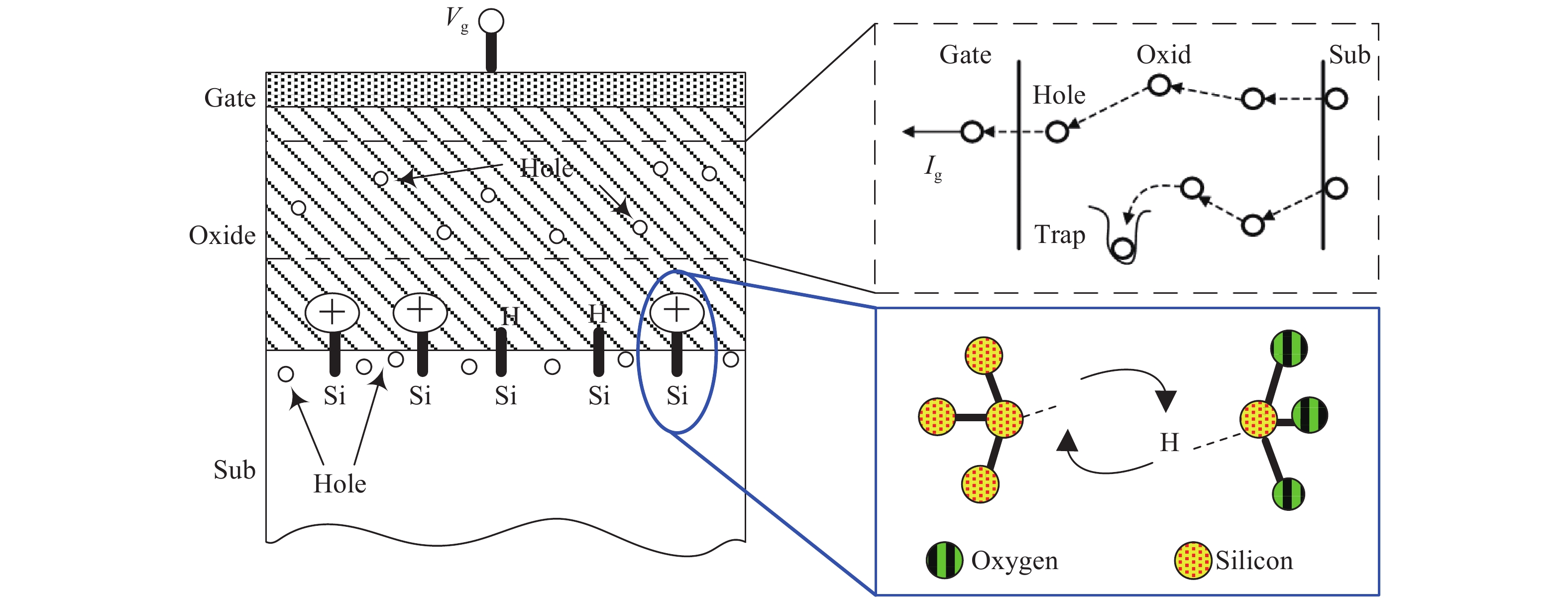
Fig. 1.
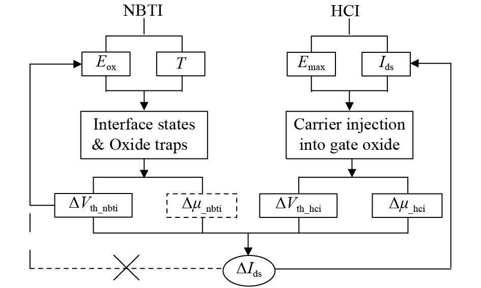
(Color online) Mechanisms of NBTI degradation, including oxide hole-trapping and interface state generation.
SEMICONDUCTOR DEVICES
Xuezhong Wu1, Chenyue Ma1, Shucheng Gao1, Xiangbin Li1, Fu Sun1, Lining Zhang2, and Xinnan Lin1,
Corresponding author: Lining Zhang, Email: lnzhang@ieee.org; Xinnan Lin, Email: xnlin@pkusz.edu.cn
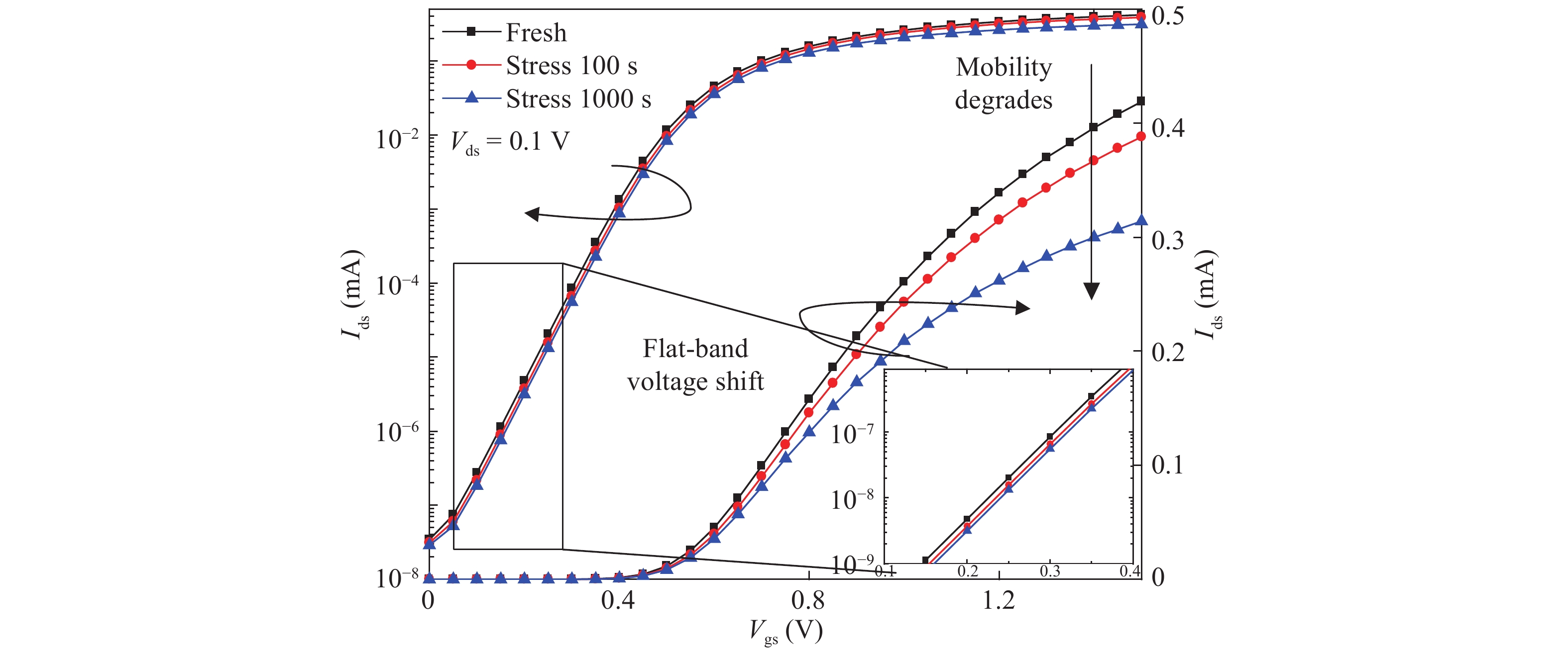
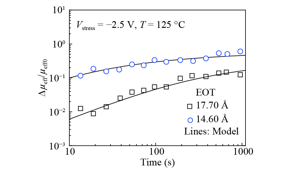
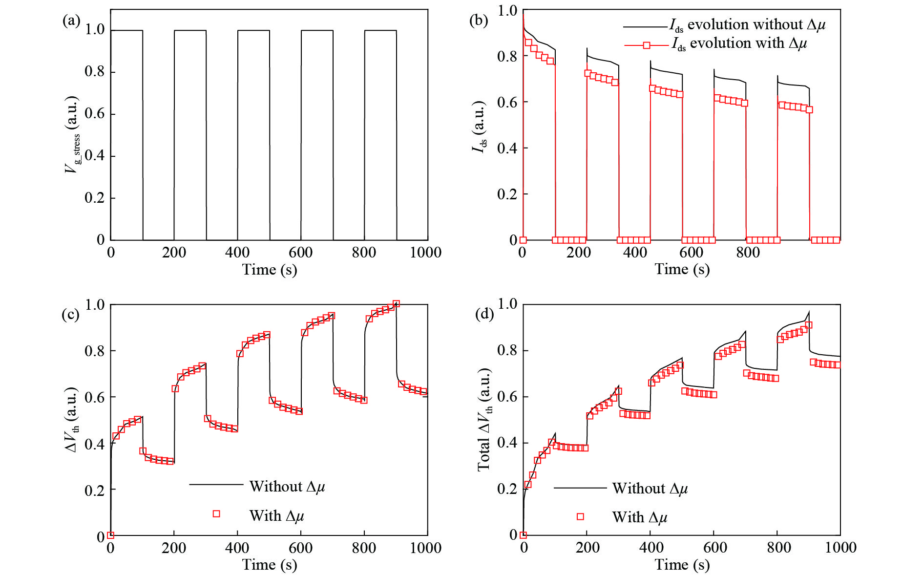
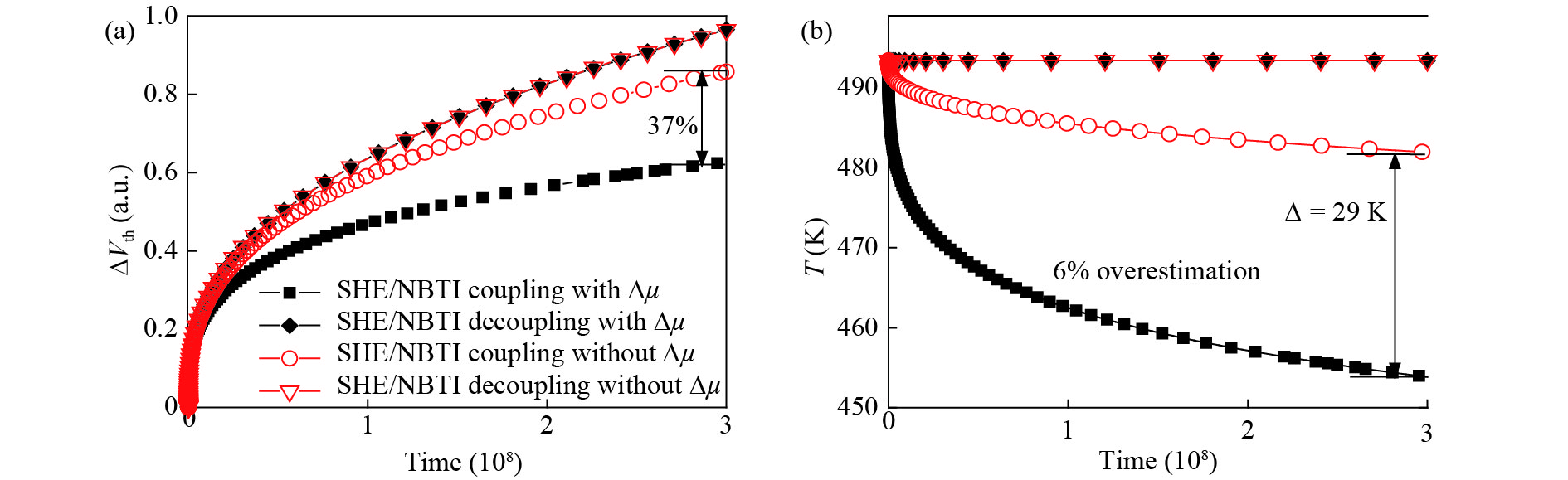
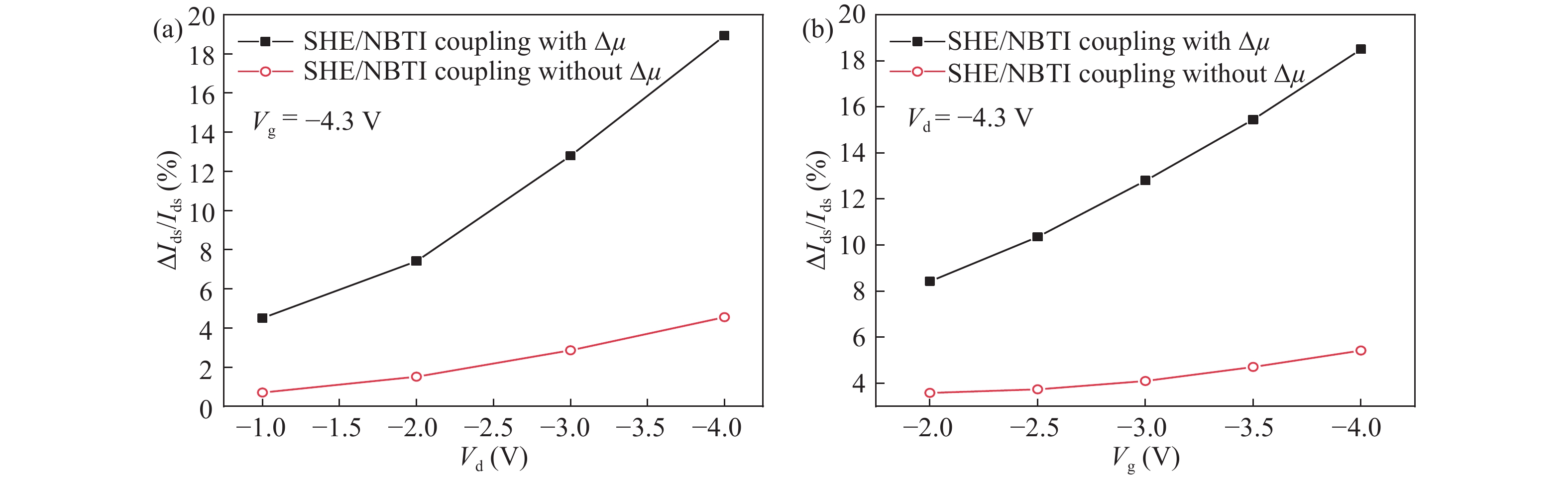
Abstract: The mobility degradation induced by negative bias temperature instability (NBTI) is usually ignored in traditional NBTI modeling and simulation, resulting in overestimation of the circuit lifetime, especially after long-term operation. In this paper, the mobility degradation is modeled in combination with the universal NBTI model. The coulomb scattering induced by interface states is revealed to be the dominant component responsible for mobility degradation. The proposed mobility degradation model fits the measured data well and provides an accurate solution for evaluating coupling of NBTI with HCI (hot carrier injection) and SHE (self-heating effect), which indicates that mobility degradation should be considered in long-term circuit aging simulation.
Key words: NBTI, mobility degradation, aging simulation algorithm, hot carrier injection, self-heating effect, coupling
| [1] |
Islam A E, Kufluoglu H, Varghese D, et al. Recent issues in negative-bias temperature instability: initial degradation, field dependence of interface trap generation, hole trapping effects, and relaxation. IEEE Trans Electron Devices, 2007, 54(9): 2143 doi: 10.1109/TED.2007.902883
|
| [2] |
Grasser T, Reisinger H, Wagner P, et al. Time-dependent defect spectroscopy for characterization of border traps in metal-oxide-semiconductor transistors. Phys Rev B, 2010, 82(24): 1771
|
| [3] |
Huard V, Denais M, Parthasarathy C. NBTI degradation: From physical mechanisms to modelling. Microelectron Relia, 2006, 46(1): 1 doi: 10.1016/j.microrel.2005.02.001
|
| [4] |
Mahapatra S, Alam M A. Defect generation in p-MOSFETs under negative-bias stress: an experimental perspective. IEEE Trans Device Mater Reliab, 2008, 8(1): 35 doi: 10.1109/TDMR.2007.912261
|
| [5] |
Tu R H, Rosenbaum E, Chan W Y, et al. Berkeley reliability tools-BERT. IEEE Trans Comput-Aided Des Integr Circuits Syst, 1993, 12(10): 1524 doi: 10.1109/43.256927
|
| [6] |
Bogdan, Tudor, Joddy, et al. MOSRA: An efficient and versatile MOS aging modeling and reliability analysis solution for 45nm and below. IEEE International Conference on Solid-State and Integrated Circuit Technology, 2010: 1645
|
| [7] |
Ma C, Li X, Sun F, et al. Investigation of the NBTI induced mobility degradation for precise circuit aging simulation. IEEE Nanoelectronics Conference, 2016: 1
|
| [8] |
Zhang L N, Ma C Y, Chan M S. Reliability-aware device compact, modeling and implications on circuit aging simulations. Workshop on Compact Modeling (WCM), Washington D.C., USA, 2016
|
| [9] |
Semenov O, Vassighi A, Sachdev M. Impact of self-heating effect on long-term reliability and performance degradation in CMOS circuits. IEEE Trans Device Mater Reliab, 2006, 6(1): 17 doi: 10.1109/TDMR.2006.870340
|
| [10] |
Grasser T, Kaczer B. Evidence that two tightly coupled mechanisms are responsible for negative bias temperature instability in oxynitride MOSFETs. IEEE Trans Electron Devices, 2009, 56(5): 1056 doi: 10.1109/TED.2009.2015160
|
| [11] |
Ma C. Universal NBTI compact model for circuit aging simulation under any stress conditions. IEEE Trans Device Mater Reliab, 2014, 14(3): 818 doi: 10.1109/TDMR.2014.2322673
|
| [12] |
Ma C, Zhang L, Lin X, et al. Universal framework for temperature dependence prediction of the negative bias temperature instability based on microscope pictures. Jpn J Appl Phys, 2016, 55(4): 044201 doi: 10.7567/JJAP.55.044201
|
| [13] |
Takagi S, Toriumi A, Iwase M, et al. On the universality of inversion layer mobility in Si MOSFET's: Part I-effects of substrate impurity concentration. IEEE Trans Electron Devices, 2002, 41(12): 2357
|
| [14] |
Cheng B, Woo J. A temperature-dependent MOSFET inversion layer carrier mobility model for device and circuit simulation. IEEE Trans Electron Devices, 2002, 44(2): 343
|
| [15] |
Villa S, Lacaita A L, Perron L M, et al. A physically-based model of the effective mobility in heavily-doped n-MOSFETs. IEEE Trans Electron Devices, 1998, 45(1): 110 doi: 10.1109/16.658819
|
| [16] |
Islam A E, Maheta V D, Das H, et al. Mobility degradation due to interface traps in plasma oxynitride PMOS devices. Reliability Physics Symposium, 2008: 87
|
| [17] |
Fukuda K, Masubuchi S, Masubuchi K. A physical and SPICE mobility degradation analysis for NBTI. IEEE Trans Electron Devices, 2013, 60(7): 2096 doi: 10.1109/TED.2013.2259493
|
| [18] |
Song M, Macwilliams K P, Woo J C S. Comparison of NMOS and PMOS hot carrier effects from 300 to 77 K. IEEE Trans Electron Devices, 1997, 44(2): 268 doi: 10.1109/16.557714
|
| [19] |
Doyle B S, Mistry K R. A lifetime prediction method for hot-carrier degradation in surface-channel p-MOS devices. IEEE Trans Electron Devices, 1990, 37(5): 1301 doi: 10.1109/16.108192
|
| [20] |
Ma C, Mattausch H J, Miyake M, et al. Compact reliability model for degradation of advanced p-MOSFETs due to NBTI and hot-carrier effects in the circuit simulation. IEEE Reliability Physics Symposium, 2013: 2A.3.1
|
| [21] |
Li X, Ma C, Zhang L, et al. Dynamic NBTI simulation coupling with self-heating effect in SOI MOSFETs. IEEE Physical and Failure Analysis of Integrated Circuits, 2016
|


Article views: 3697 Times PDF downloads: 110 Times Cited by: 0 Times
Received: 21 February 2018 Revised: 24 September 2018 Online: Accepted Manuscript: 05 November 2018Uncorrected proof: 12 November 2018Published: 13 December 2018
| Citation: |
Xuezhong Wu, Chenyue Ma, Shucheng Gao, Xiangbin Li, Fu Sun, Lining Zhang, Xinnan Lin. Model of NBTI combined with mobility degradation[J]. Journal of Semiconductors, 2018, 39(12): 124015. doi: 10.1088/1674-4926/39/12/124015
X Z Wu, C Y Ma, S C Gao, X B Li, F Sun, L N Zhang, X N Lin, Model of NBTI combined with mobility degradation[J]. J. Semicond., 2018, 39(12): 124015. doi: 10.1088/1674-4926/39/12/124015.
Export: BibTex EndNote

|
| [1] |
Islam A E, Kufluoglu H, Varghese D, et al. Recent issues in negative-bias temperature instability: initial degradation, field dependence of interface trap generation, hole trapping effects, and relaxation. IEEE Trans Electron Devices, 2007, 54(9): 2143 doi: 10.1109/TED.2007.902883
|
| [2] |
Grasser T, Reisinger H, Wagner P, et al. Time-dependent defect spectroscopy for characterization of border traps in metal-oxide-semiconductor transistors. Phys Rev B, 2010, 82(24): 1771
|
| [3] |
Huard V, Denais M, Parthasarathy C. NBTI degradation: From physical mechanisms to modelling. Microelectron Relia, 2006, 46(1): 1 doi: 10.1016/j.microrel.2005.02.001
|
| [4] |
Mahapatra S, Alam M A. Defect generation in p-MOSFETs under negative-bias stress: an experimental perspective. IEEE Trans Device Mater Reliab, 2008, 8(1): 35 doi: 10.1109/TDMR.2007.912261
|
| [5] |
Tu R H, Rosenbaum E, Chan W Y, et al. Berkeley reliability tools-BERT. IEEE Trans Comput-Aided Des Integr Circuits Syst, 1993, 12(10): 1524 doi: 10.1109/43.256927
|
| [6] |
Bogdan, Tudor, Joddy, et al. MOSRA: An efficient and versatile MOS aging modeling and reliability analysis solution for 45nm and below. IEEE International Conference on Solid-State and Integrated Circuit Technology, 2010: 1645
|
| [7] |
Ma C, Li X, Sun F, et al. Investigation of the NBTI induced mobility degradation for precise circuit aging simulation. IEEE Nanoelectronics Conference, 2016: 1
|
| [8] |
Zhang L N, Ma C Y, Chan M S. Reliability-aware device compact, modeling and implications on circuit aging simulations. Workshop on Compact Modeling (WCM), Washington D.C., USA, 2016
|
| [9] |
Semenov O, Vassighi A, Sachdev M. Impact of self-heating effect on long-term reliability and performance degradation in CMOS circuits. IEEE Trans Device Mater Reliab, 2006, 6(1): 17 doi: 10.1109/TDMR.2006.870340
|
| [10] |
Grasser T, Kaczer B. Evidence that two tightly coupled mechanisms are responsible for negative bias temperature instability in oxynitride MOSFETs. IEEE Trans Electron Devices, 2009, 56(5): 1056 doi: 10.1109/TED.2009.2015160
|
| [11] |
Ma C. Universal NBTI compact model for circuit aging simulation under any stress conditions. IEEE Trans Device Mater Reliab, 2014, 14(3): 818 doi: 10.1109/TDMR.2014.2322673
|
| [12] |
Ma C, Zhang L, Lin X, et al. Universal framework for temperature dependence prediction of the negative bias temperature instability based on microscope pictures. Jpn J Appl Phys, 2016, 55(4): 044201 doi: 10.7567/JJAP.55.044201
|
| [13] |
Takagi S, Toriumi A, Iwase M, et al. On the universality of inversion layer mobility in Si MOSFET's: Part I-effects of substrate impurity concentration. IEEE Trans Electron Devices, 2002, 41(12): 2357
|
| [14] |
Cheng B, Woo J. A temperature-dependent MOSFET inversion layer carrier mobility model for device and circuit simulation. IEEE Trans Electron Devices, 2002, 44(2): 343
|
| [15] |
Villa S, Lacaita A L, Perron L M, et al. A physically-based model of the effective mobility in heavily-doped n-MOSFETs. IEEE Trans Electron Devices, 1998, 45(1): 110 doi: 10.1109/16.658819
|
| [16] |
Islam A E, Maheta V D, Das H, et al. Mobility degradation due to interface traps in plasma oxynitride PMOS devices. Reliability Physics Symposium, 2008: 87
|
| [17] |
Fukuda K, Masubuchi S, Masubuchi K. A physical and SPICE mobility degradation analysis for NBTI. IEEE Trans Electron Devices, 2013, 60(7): 2096 doi: 10.1109/TED.2013.2259493
|
| [18] |
Song M, Macwilliams K P, Woo J C S. Comparison of NMOS and PMOS hot carrier effects from 300 to 77 K. IEEE Trans Electron Devices, 1997, 44(2): 268 doi: 10.1109/16.557714
|
| [19] |
Doyle B S, Mistry K R. A lifetime prediction method for hot-carrier degradation in surface-channel p-MOS devices. IEEE Trans Electron Devices, 1990, 37(5): 1301 doi: 10.1109/16.108192
|
| [20] |
Ma C, Mattausch H J, Miyake M, et al. Compact reliability model for degradation of advanced p-MOSFETs due to NBTI and hot-carrier effects in the circuit simulation. IEEE Reliability Physics Symposium, 2013: 2A.3.1
|
| [21] |
Li X, Ma C, Zhang L, et al. Dynamic NBTI simulation coupling with self-heating effect in SOI MOSFETs. IEEE Physical and Failure Analysis of Integrated Circuits, 2016
|

 WeChat ID
Journal of Semiconductors © 2017 All Rights Reserved 京ICP备05085259号-2

 DownLoad: