


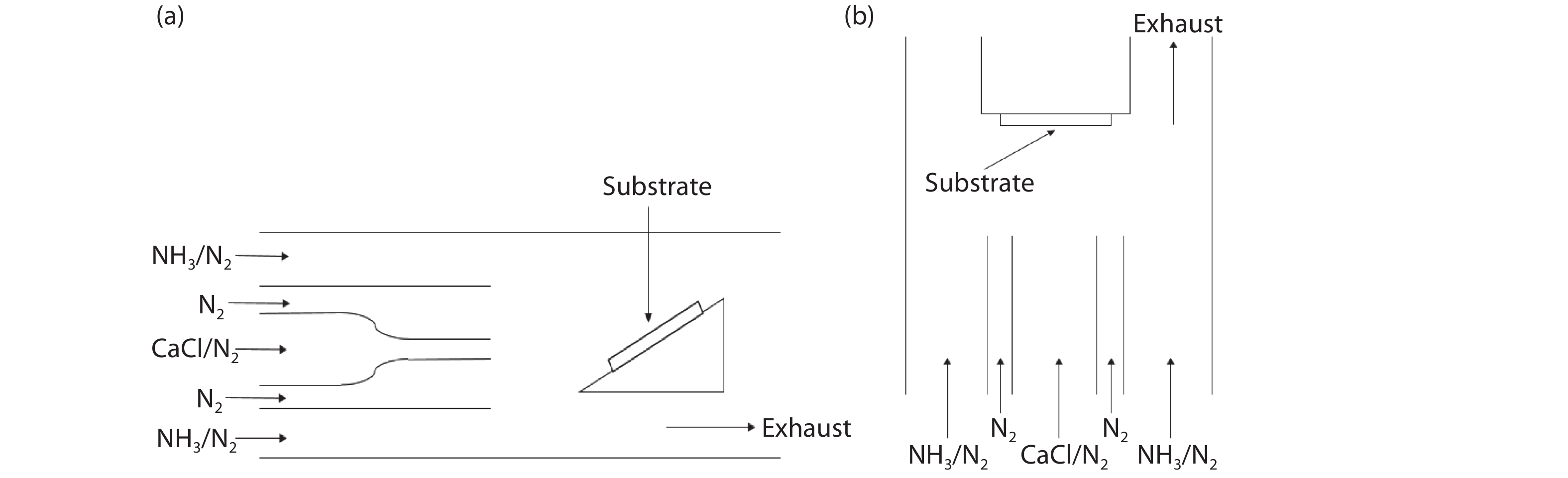
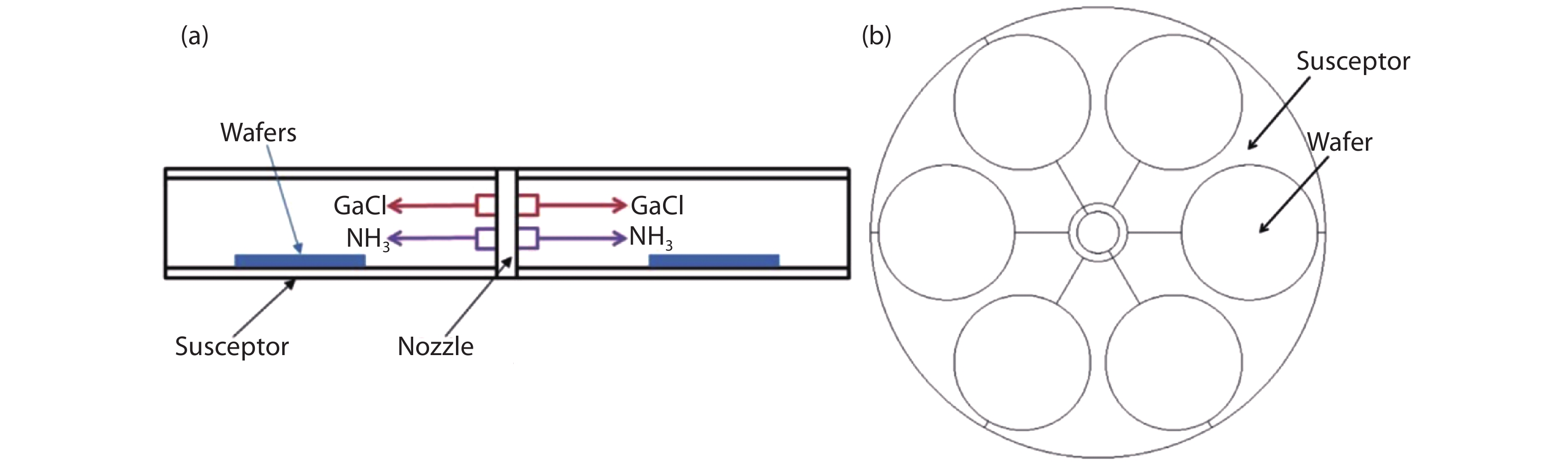
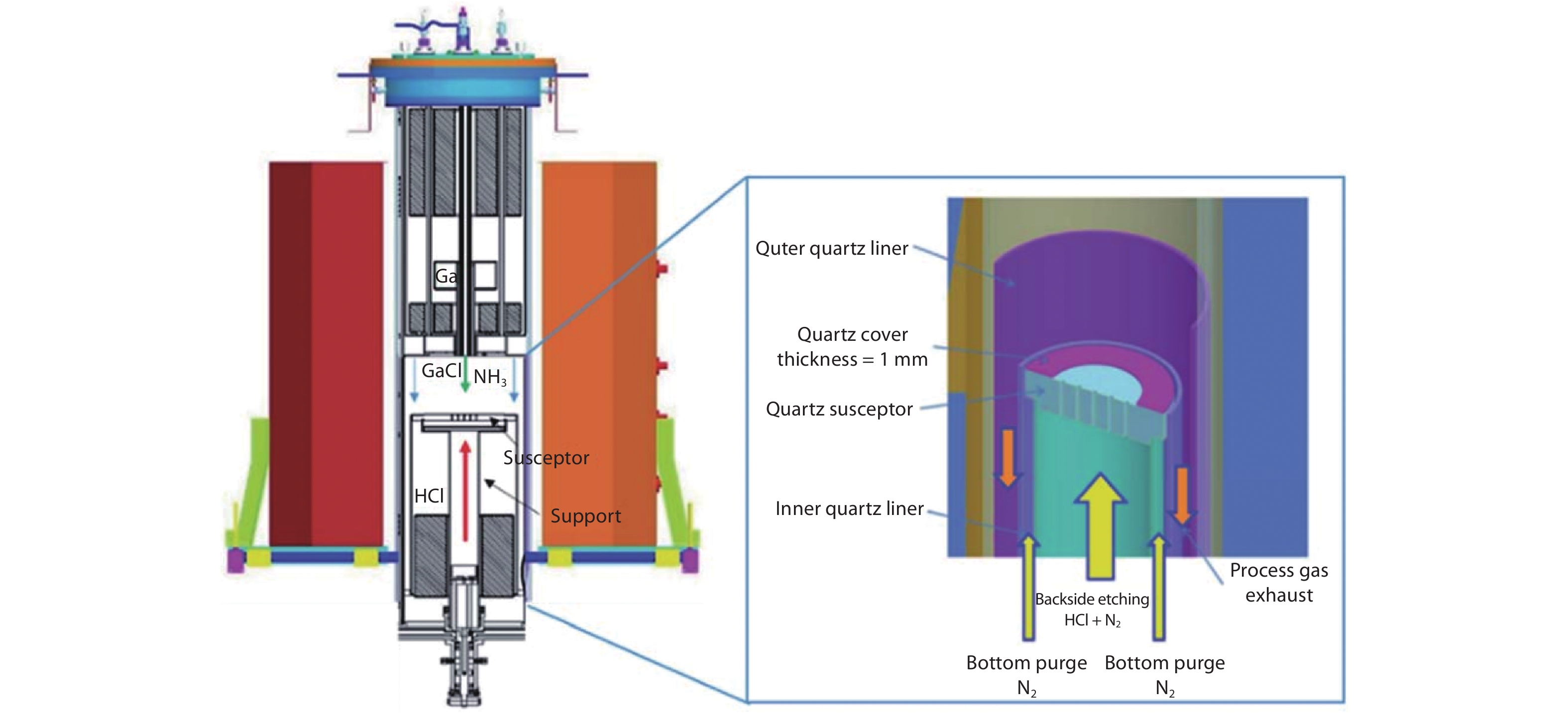
Fig. 1.
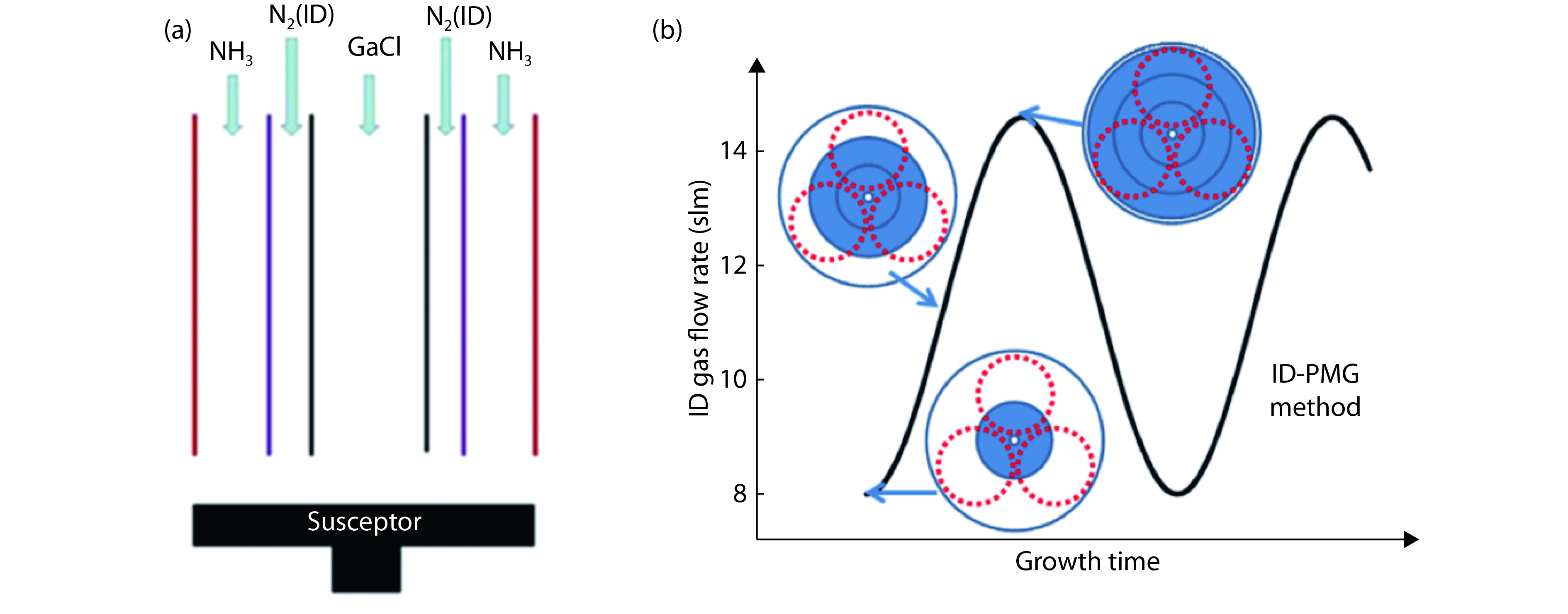
Schematic view of (a) horizontal HVPE reactor and (b) vertical HVPE reactor.
REVIEWS
Jun Hu1, 2, , Hongyuan Wei1, 2, , Shaoyan Yang1, 2, , Chengming Li1, 2, Huijie Li1, 2, Xianglin Liu1, 2, Lianshan Wang1, 2 and Zhanguo Wang1, 2
Corresponding author: Jun Hu, E-mail: hujun@semi.ac.cn; Hongyuan Wei, E-mail: why@semi.ac.cn; Shaoyan Yang, E-mail: sh-yyang@semi.ac.cn
Abstract: Due to the remarkable growth rate compared to another growth methods for gallium nitride (GaN) growth, hydride vapor phase epitaxy (HVPE) is now the only method for mass product GaN substrates. In this review, commercial HVPE systems and the GaN crystals grown by them are demonstrated. This article also illustrates some innovative attempts to develop homebuilt HVPE systems. Finally, the prospects for the further development of HVPE for GaN crystal growth in the future are also discussed.
Key words: hydride vapor phase epitaxy, gallium nitride, substrate
| [1] |
Van Vechten J A. Quantum dielectric theory of electronegativity in covalent systems. III. pressure-temperature phase diagrams, heats of mixing, and distribution coefficients. Phys Rev B, 1973, 7, 1479 doi: 10.1103/PhysRevB.7.1479
|
| [2] |
Karpiński J, Jun J, Porowski S. Equilibrium pressure of N2 over GaN and high pressure solution growth of GaN. J Cryst Growth, 1984, 66, 1 doi: 10.1016/0022-0248(84)90070-8
|
| [3] |
Leszcynski M, Grzegory I, Bockowski M. X-ray examination of GaN single crystals grown at high hydrostatic pressure. J Cryst Growth, 1993, 126, 601 doi: 10.1016/0022-0248(93)90809-B
|
| [4] |
Yamane H, Shimada M, Clarke S J, et al. Preparation of GaN single crystals using a Na flux. Chem Mater, 1997, 9, 413 doi: 10.1021/cm960494s
|
| [5] |
Murakami K, Matsuo D, Imabayashi H, et al. Effects of solution stirring on the growth of bulk GaN single crystals by Na flux method. Jpn J Appl Phys, 2013, 52, 08JA03 doi: 10.7567/JJAP.52.08JA03
|
| [6] |
Dwiliński R, Doradziński R, Garczyński J, et al. Excellent crystallinity of truly bulk ammonothermal GaN. J Cryst Growth, 2008, 310, 3911 doi: 10.1016/j.jcrysgro.2008.06.036
|
| [7] |
Ehrentraut D, Pakalapati R T, Kamber D S, et al. High quality, low cost ammonothermal bulk gan substrates. Jpn J Appl Phys, 2013, 52, 08JA01 doi: 10.7567/JJAP.52.08JA01
|
| [8] |
Kelly M K, Vaudo R P, Phanse V M, et al. Large free-standing GaN substrates by hydride vapor phase epitaxy and laser-induced liftoff. Jpn J Appl Phys, 1999, 38, L217 doi: 10.1143/JJAP.38.L217
|
| [9] |
Motoki K, Okahisa T, Matsumoto N, et al. Preparation of large freestanding GaN substrates by hydride vapor phase epitaxy using GaAs as a starting substrate. Jpn J Appl Phys, 2001, 40, L140 doi: 10.1143/JJAP.40.L140
|
| [10] |
Oshima Y, Eri T, Shibata M, et al. Preparation of freestanding GaN wafers by hydride vapor phase epitaxy with void-assisted separation. Jpn J Appl Phys, 2003, 42, L1 doi: 10.1143/JJAP.42.L1
|
| [11] |
Lee M, Mikulik D, Yang M, et al. Nearly perfect GaN crystal via pit-assisted growth by HVPE. CrystEngComm, 2017, 19, 2036 doi: 10.1039/C7CE00246G
|
| [12] |
Yoshida T, Imanishi M, Kitamura T, et al. Development of GaN substrate with a large diameter and small orientation deviation. Phys Status Solidi B, 2017, 254, 1600671 doi: 10.1002/pssb.v254.8
|
| [13] |
Maruska H P, Tietjen J J. The preparation and properties of vapor-deposited single-crystal-line GaN. Appl Phys Lett, 1969, 15, 327 doi: 10.1063/1.1652845
|
| [14] |
Wickenden D K, Faulkner K R, Brander R W, et al. Growth of epitaxial layers of gallium nitride on silicon carbide and corundum substrates. J Cryst Growth, 1971, 9, 158 doi: 10.1016/0022-0248(71)90225-9
|
| [15] |
Seifert W, Fitzl G, Butter E. Study on the growth rate in VPE of GaN. J Cryst Growth, 1981, 52, 257 doi: 10.1016/0022-0248(81)90201-3
|
| [16] |
Parillaud O, Wagner V, Buehlmann H J, et al. Localized epitaxy of GaN by HVPE on patterned substrates. MRS Int J Nitride Semicond Res, 1998, 3, e40 doi: 10.1557/S1092578300001125
|
| [17] |
Richter E, Gramlich S, Klein A, et al. Direct growth of GaN on (0001) sapphire by low pressure hydride vapour phase epitaxy. Phys Status Solidi A, 2001, 188, 439 doi: 10.1002/(ISSN)1521-396X
|
| [18] |
Hennig C, Richter E, Weyers M, et al. Self-separation of thick two inch GaN layers grown by HVPE on sapphire using epitaxial lateral overgrowth with masks containing tungsten. Phys Status Solidi C, 2007, 4, 2638 doi: 10.1002/(ISSN)1610-1642
|
| [19] |
Wang C, Anthony C H, Seyboth M, et al. Influence of growth parameters on crack density in thick epitaxially lateral overgrown GaN layers by hydride vapor phase epitaxy. J Cryst Growth, 2001, 230, 377 doi: 10.1016/S0022-0248(01)01298-2
|
| [20] |
Hemmingsson C, Paskov P P, Pozina G, et al. Growth of bulk GaN in a vertical hydride vapour phase epitaxy reactor. Superlattices Microstruct, 2006, 40, 205 doi: 10.1016/j.spmi.2006.09.014
|
| [21] |
Richter E, Hennig C, Weyers M, et al. Reactor and growth process optimization for growth of thick GaN layers on sapphire substrates by HVPE. J Cryst Growth, 2005, 277, 6 doi: 10.1016/j.jcrysgro.2004.12.169
|
| [22] |
Schineller B, Kaeppeler J, Heuken M. Vertical-HVPE as a production method for free-standing GaN-substrates. Konferenzprotokoll, AIXTRON AG, Austin, Texas, 2007
|
| [23] |
https://compoundsemiconductor.net/article/84531/Aixtron_takes_HVPE_vertical_for_cheap_GaN_substrates, Aixtron takes HVPE vertical for cheap GaN substrates - News
|
| [24] |
Hemmingsson C, Paskov P P, Pozina G, et al. Hydride vapour phase epitaxy growth and characterization of thick GaN using a vertical HVPE reactor. J Cryst Growth, 2007, 300, 32 doi: 10.1016/j.jcrysgro.2006.10.223
|
| [25] |
Richter E, Zeimer U, Hagedorn S, et al. Hydride vapor phase epitaxy of GaN boules using high growth rates. J Cryst Growth, 2010, 312, 2537 doi: 10.1016/j.jcrysgro.2010.04.009
|
| [26] |
Richter E, Gründer M, Schineller B, et al. GaN boules grown by high rate HVPE. Phys Status Solidi C, 2011, 8, 1450 doi: 10.1002/pssc.201000901
|
| [27] |
Richter E, Gründer M, Netzel C, et al. Growth of GaN boules via vertical HVPE. J Cryst Growth, 2012, 350, 89 doi: 10.1016/j.jcrysgro.2011.12.030
|
| [28] |
http://www.kymatech.com/news/224-kyma-adds-gallium-oxide-epiwafers-to-its-product-portfolio-2, Kyma Enters Gallium Nitride Crystal Growth Equipment Market
|
| [29] |
http://www.kymatech.com/products/crystal-growth-tools/545-hydride-vapor-phase-epitaxy-hvpe-growth-tool, K200TM HVPE Growth Tools
|
| [30] |
Shin H, Thomson D B, Schlesser R, et al. High temperature nucleation and growth of GaN crystals from the vapor phase. J Cryst Growth, 2002, 241, 404 doi: 10.1016/S0022-0248(02)01290-3
|
| [31] |
Bohnen T, Ashraf H, van Dreumel G W G, et al. Enhanced growth rates and reduced parasitic deposition by the substitution of Cl2 for HCl in GaN HVPE. J Cryst Growth, 2010(312), 2542 doi: 10.1016/j.jcrysgro.2010.04.010
|
| [32] |
Nakamura D, Kimura T, Horibuchi K. Halogen-free vapor phase epitaxy for high-rate growth of GaN bulk crystals. Appl Phys Express, 2017, 10, 045504 doi: 10.7567/APEX.10.045504
|
| [33] |
Nakamura D, Kimura T. Significant increase in GaN growth rate by halogen-free vapor phase epitaxy with porosity-controlled evaporator. Appl Phys Express, 2017, 10, 095503 doi: 10.7567/APEX.10.095503
|
| [34] |
Nakamura D, Kimura T. Ultrahigh-yield growth of GaN via halogen-free vapor-phase epitaxy. Appl Phys Express, 2018, 11, 065502 doi: 10.7567/APEX.11.065502
|
| [35] |
Kimura T, Horibuchi K, Kataoka K, et al. Macro-defect-free homoepitaxial GaN growth through halogen-free vapor-phase epitaxy on native GaN seeds. J Cryst Growth, 2018, 494, 17 doi: 10.1016/j.jcrysgro.2018.05.002
|
| [36] |
Nakamura D, Suzumura A, Shigetoh K. Sintered tantalum carbide coatings on graphite substrates: Highly reliable protective coatings for bulk and epitaxial growth. Appl Phys Lett, 2015, 106, 082108 doi: 10.1063/1.4913413
|
| [37] |
Nakamura D. Simple and quick enhancement of SiC bulk crystal growth using a newly developed crucible material. Appl Phys Express, 2016, 9, 055507 doi: 10.7567/APEX.9.055507
|
| [38] |
Nakamura D, Shigetoh K, Suzumura A. Tantalum carbide coating via wet powder process: From slurry design to practical process tests. J Eur Ceram Soc, 2017, 37, 1175 doi: 10.1016/j.jeurceramsoc.2016.10.029
|
| [39] |
Nakamura D, Kimura T, Narita T, et al. TaC-coated graphite prepared via a wet ceramic process: Application to CVD susceptors for epitaxial growth of wide-bandgap semiconductors. J Cryst Growth, 2017, 478, 163 doi: 10.1016/j.jcrysgro.2017.09.003
|
| [40] |
Lukin G, Schneider T, Barchuk M, et al. Modified high temperature vapor phase epitaxy for growth of GaN films: Modified HTVPE for growth of GaN films. Phys Status Solidi A, 2017, 214, 1600753 doi: 10.1002/pssa.v214.9
|
| [41] |
Schneider T, Lukin G, Zimmermann F, et al. Studies on high temperature vapor phase epitaxy of GaN. J Cryst Growth, 2017, 468, 212 doi: 10.1016/j.jcrysgro.2016.10.080
|
| [42] |
Lukin G, Röder C, Barchuk M, et al. Investigation of GaN layers grown by high temperature vapor phase epitaxy: Investigation of GaN layers grown by high temperature vapor phase epitaxy. Phys Status Solidi C, 2014, 11, 491 doi: 10.1002/pssc.v11.3/4
|
| [43] |
Yuri M, Ueda T, Lee H, et al. Vapor phase epitaxy of GaN using gallium tri-chloride and ammonia. In: Compound Semiconductor Electronics and Photonics. Vol. 421. Pittsburgh: Materials Research Soc, 1996, 195
|
| [44] |
Takahashi N, Matsumoto R, Koukitu A, et al. Vapor phase epitaxy of InxGa1–xN using InCl3, GaCl3 and NH3 sources. Jpn J Appl Phys Part 2-Lett, 1997, 36, L601 doi: 10.1143/JJAP.36.L601
|
| [45] |
Topf M, Steude G, Fischer S, et al. 1998 Low-pressure chemical vapor deposition of GaN epitaxial films. J Cryst Growth, 1998, 189/190, 330 doi: 10.1016/S0022-0248(98)00285-1
|
| [46] |
Varadarajan E, Puviarasu P, Kumar J, et al. On the chloride vapor-phase epitaxy growth of GaN and its characterization. J Cryst Growth, 2004, 260, 43 doi: 10.1016/j.jcrysgro.2003.08.021
|
| [47] |
Murakami H, Takekawa N, Shiono A, et al. Tri-halide vapor phase epitaxy of thick GaN using gaseous GaCl3 precursor. J Cryst Growth, 2016, 456, 140 doi: 10.1016/j.jcrysgro.2016.08.029
|
| [48] |
Kumagai Y, Takemoto K, Hasegawa T, et al. Thermodynamics on tri-halide vapor-phase epitaxy of GaN and InxGa1–xN using GaCl3 and InCl3. J Cryst Growth, 2001, 231, 57 doi: 10.1016/S0022-0248(01)01453-1
|
| [49] |
Yamane T, Hanaoka K, Murakami H, et al. Tri-halide vapor phase epitaxy of GaN using GaCl3 gas as a group III precursor Phys. Status Solidi C, 2011, 8, 1471 doi: 10.1002/pssc.201000902
|
| [50] |
Iso K, Takekawa N, Matsuda K, et al. Tri-halide vapor-phase epitaxy of GaN using GaCl3 on polar, semipolar, and nonpolar substrates. Appl Phys Express, 2016, 9, 105501 doi: 10.7567/APEX.9.105501
|
| [51] |
Yoshida T, Oshima Y, Watanabe K, et al. Ultrahigh-speed growth of GaN by hydride vapor phase epitaxy. Phys Status Solidi C, 2011, 8, 2110 doi: 10.1002/pssc.201000953
|
| [52] |
Gil E, André Y, Cadoret R, et al. Hydride vapor phase epitaxy for current III–V and nitride semiconductor compound issues. In: Handbook of Crystal Growth. 2nd ed. Boston: North-Holland 2015, 51
|
| [53] |
Takekawa N, Hayashida N, Ohzeki D, et al. Growth temperatures and the excess chlorine effect of N-polar GaN growth via tri-halide vapor phase epitaxy. J Cryst Growth, 2018, 502, 7 doi: 10.1016/j.jcrysgro.2018.08.024
|
| [54] |
Iso K, Matsuda K, Takekawa N, et al. Quasiequilibrium crystal shape and kinetic Wulff plot for GaN grown by trihalide vapor phase epitaxy using GaCl3. Phys Status Solidi B, 2017, 254, 1600679 doi: 10.1002/pssb.201600679
|
| [55] |
Iso K, Matsuda K, Takekawa N, et al. Thick nonpolar m-plane and semipolar (10(1)over-bar(1)over-bar) GaN on an ammonothermal seed by tri-halide vapor-phase epitaxy using GaCl3. J Cryst Growth, 2017, 461, 25 doi: 10.1016/j.jcrysgro.2017.01.005
|
| [56] |
Liu N, Wu J, Li W, et al. Highly uniform growth of 2-inch GaN wafers with a multi-wafer HVPE system. J Cryst Growth, 2014, 388, 132 doi: 10.1016/j.jcrysgro.2013.11.023
|
| [57] |
Cheng Y, Liu P, Wu J, et al. High uniform growth of 4-inch GaN wafer via flow field optimization by HVPE. J Cryst Growth, 2016, 445, 24 doi: 10.1016/j.jcrysgro.2016.04.010
|
| [58] |
Han X F, Hur M J, Lee J H, et al. Numerical simulation of the gallium nitride thin film layer grown on 6-inch wafer by commercial multi-wafer hydride vapor phase epitaxy. J Cryst Growth, 2014, 406, 53 doi: 10.1016/j.jcrysgro.2014.08.018
|
| [59] |
Han X F, Lee J H, Lee Y J, et al. Numerical analysis on the origin of thickness unevenness and formation of pits at GaN thin film grown by HVPE. J Cryst Growth, 2016, 450, 66 doi: 10.1016/j.jcrysgro.2016.06.015
|
| [60] |
Han X F, Lee J H, Lee Y J, et al. 3D numerical analysis of influence of the non-uniform deposition rate on the hillock density at HVPE-GaN surface. J Cryst Growth, 2017, 474, 81 doi: 10.1016/j.jcrysgro.2016.12.081
|
| [61] |
Luo W, Wu J, Goldsmith J, et al. The growth of high-quality and self-separation GaN thick-films by hydride vapor phase epitaxy. J Cryst Growth, 2012, 340, 18 doi: 10.1016/j.jcrysgro.2011.11.037
|
| [62] |
Amilusik M, Sochacki T, Łucznik B, et al. Analysis of self-lift-off process during HVPE growth of GaN on MOCVD-GaN/sapphire substrates with photolitographically patterned Ti mask. J Cryst Growth, 2013, 380, 99 doi: 10.1016/j.jcrysgro.2013.06.005
|
| [63] |
Sui Y, Wang B, Zhao Z, et al. Facet growth of self-separated GaN layers through HVPE on large square-patterned template. J Cryst Growth, 2014, 394, 11 doi: 10.1016/j.jcrysgro.2014.01.059
|
| [64] |
Lee M, Mikulik D, Yang M, et al. The investigation of stress in freestanding GaN crystals grown from Si substrates by HVPE. Sci Rep, 2017, 7, 8587 doi: 10.1038/s41598-017-08905-y
|
| [65] |
Lee M, Mikulik D, Kim J, et al. A novel growth method of freestanding GaN using in situ removal of Si substrate in hydride vapor phase epitaxy. Appl Phys Express, 2013, 6, 125502 doi: 10.7567/APEX.6.125502
|
| [66] |
Lee M, Mikulik D, Park S. The investigation of in situ removal of Si substrates for freestanding GaN crystals by HVPE. RSC Adv, 2018, 8, 12310 doi: 10.1039/C8RA01347K
|


Article views: 4884 Times PDF downloads: 154 Times Cited by: 0 Times
Received: 16 January 2019 Revised: 15 May 2019 Online: Accepted Manuscript: 14 June 2019Uncorrected proof: 18 June 2019Published: 01 October 2019
| Citation: |
Jun Hu, Hongyuan Wei, Shaoyan Yang, Chengming Li, Huijie Li, Xianglin Liu, Lianshan Wang, Zhanguo Wang. Hydride vapor phase epitaxy for gallium nitride substrate[J]. Journal of Semiconductors, 2019, 40(10): 101801. doi: 10.1088/1674-4926/40/10/101801
J Hu, H Y Wei, S Y Yang, C M Li, H J Li, X L Liu, L S Wang, Z G Wang, Hydride vapor phase epitaxy for gallium nitride substrate[J]. J. Semicond., 2019, 40(10): 101801. doi: 10.1088/1674-4926/40/10/101801.
Export: BibTex EndNote

|
| [1] |
Van Vechten J A. Quantum dielectric theory of electronegativity in covalent systems. III. pressure-temperature phase diagrams, heats of mixing, and distribution coefficients. Phys Rev B, 1973, 7, 1479 doi: 10.1103/PhysRevB.7.1479
|
| [2] |
Karpiński J, Jun J, Porowski S. Equilibrium pressure of N2 over GaN and high pressure solution growth of GaN. J Cryst Growth, 1984, 66, 1 doi: 10.1016/0022-0248(84)90070-8
|
| [3] |
Leszcynski M, Grzegory I, Bockowski M. X-ray examination of GaN single crystals grown at high hydrostatic pressure. J Cryst Growth, 1993, 126, 601 doi: 10.1016/0022-0248(93)90809-B
|
| [4] |
Yamane H, Shimada M, Clarke S J, et al. Preparation of GaN single crystals using a Na flux. Chem Mater, 1997, 9, 413 doi: 10.1021/cm960494s
|
| [5] |
Murakami K, Matsuo D, Imabayashi H, et al. Effects of solution stirring on the growth of bulk GaN single crystals by Na flux method. Jpn J Appl Phys, 2013, 52, 08JA03 doi: 10.7567/JJAP.52.08JA03
|
| [6] |
Dwiliński R, Doradziński R, Garczyński J, et al. Excellent crystallinity of truly bulk ammonothermal GaN. J Cryst Growth, 2008, 310, 3911 doi: 10.1016/j.jcrysgro.2008.06.036
|
| [7] |
Ehrentraut D, Pakalapati R T, Kamber D S, et al. High quality, low cost ammonothermal bulk gan substrates. Jpn J Appl Phys, 2013, 52, 08JA01 doi: 10.7567/JJAP.52.08JA01
|
| [8] |
Kelly M K, Vaudo R P, Phanse V M, et al. Large free-standing GaN substrates by hydride vapor phase epitaxy and laser-induced liftoff. Jpn J Appl Phys, 1999, 38, L217 doi: 10.1143/JJAP.38.L217
|
| [9] |
Motoki K, Okahisa T, Matsumoto N, et al. Preparation of large freestanding GaN substrates by hydride vapor phase epitaxy using GaAs as a starting substrate. Jpn J Appl Phys, 2001, 40, L140 doi: 10.1143/JJAP.40.L140
|
| [10] |
Oshima Y, Eri T, Shibata M, et al. Preparation of freestanding GaN wafers by hydride vapor phase epitaxy with void-assisted separation. Jpn J Appl Phys, 2003, 42, L1 doi: 10.1143/JJAP.42.L1
|
| [11] |
Lee M, Mikulik D, Yang M, et al. Nearly perfect GaN crystal via pit-assisted growth by HVPE. CrystEngComm, 2017, 19, 2036 doi: 10.1039/C7CE00246G
|
| [12] |
Yoshida T, Imanishi M, Kitamura T, et al. Development of GaN substrate with a large diameter and small orientation deviation. Phys Status Solidi B, 2017, 254, 1600671 doi: 10.1002/pssb.v254.8
|
| [13] |
Maruska H P, Tietjen J J. The preparation and properties of vapor-deposited single-crystal-line GaN. Appl Phys Lett, 1969, 15, 327 doi: 10.1063/1.1652845
|
| [14] |
Wickenden D K, Faulkner K R, Brander R W, et al. Growth of epitaxial layers of gallium nitride on silicon carbide and corundum substrates. J Cryst Growth, 1971, 9, 158 doi: 10.1016/0022-0248(71)90225-9
|
| [15] |
Seifert W, Fitzl G, Butter E. Study on the growth rate in VPE of GaN. J Cryst Growth, 1981, 52, 257 doi: 10.1016/0022-0248(81)90201-3
|
| [16] |
Parillaud O, Wagner V, Buehlmann H J, et al. Localized epitaxy of GaN by HVPE on patterned substrates. MRS Int J Nitride Semicond Res, 1998, 3, e40 doi: 10.1557/S1092578300001125
|
| [17] |
Richter E, Gramlich S, Klein A, et al. Direct growth of GaN on (0001) sapphire by low pressure hydride vapour phase epitaxy. Phys Status Solidi A, 2001, 188, 439 doi: 10.1002/(ISSN)1521-396X
|
| [18] |
Hennig C, Richter E, Weyers M, et al. Self-separation of thick two inch GaN layers grown by HVPE on sapphire using epitaxial lateral overgrowth with masks containing tungsten. Phys Status Solidi C, 2007, 4, 2638 doi: 10.1002/(ISSN)1610-1642
|
| [19] |
Wang C, Anthony C H, Seyboth M, et al. Influence of growth parameters on crack density in thick epitaxially lateral overgrown GaN layers by hydride vapor phase epitaxy. J Cryst Growth, 2001, 230, 377 doi: 10.1016/S0022-0248(01)01298-2
|
| [20] |
Hemmingsson C, Paskov P P, Pozina G, et al. Growth of bulk GaN in a vertical hydride vapour phase epitaxy reactor. Superlattices Microstruct, 2006, 40, 205 doi: 10.1016/j.spmi.2006.09.014
|
| [21] |
Richter E, Hennig C, Weyers M, et al. Reactor and growth process optimization for growth of thick GaN layers on sapphire substrates by HVPE. J Cryst Growth, 2005, 277, 6 doi: 10.1016/j.jcrysgro.2004.12.169
|
| [22] |
Schineller B, Kaeppeler J, Heuken M. Vertical-HVPE as a production method for free-standing GaN-substrates. Konferenzprotokoll, AIXTRON AG, Austin, Texas, 2007
|
| [23] |
https://compoundsemiconductor.net/article/84531/Aixtron_takes_HVPE_vertical_for_cheap_GaN_substrates, Aixtron takes HVPE vertical for cheap GaN substrates - News
|
| [24] |
Hemmingsson C, Paskov P P, Pozina G, et al. Hydride vapour phase epitaxy growth and characterization of thick GaN using a vertical HVPE reactor. J Cryst Growth, 2007, 300, 32 doi: 10.1016/j.jcrysgro.2006.10.223
|
| [25] |
Richter E, Zeimer U, Hagedorn S, et al. Hydride vapor phase epitaxy of GaN boules using high growth rates. J Cryst Growth, 2010, 312, 2537 doi: 10.1016/j.jcrysgro.2010.04.009
|
| [26] |
Richter E, Gründer M, Schineller B, et al. GaN boules grown by high rate HVPE. Phys Status Solidi C, 2011, 8, 1450 doi: 10.1002/pssc.201000901
|
| [27] |
Richter E, Gründer M, Netzel C, et al. Growth of GaN boules via vertical HVPE. J Cryst Growth, 2012, 350, 89 doi: 10.1016/j.jcrysgro.2011.12.030
|
| [28] |
http://www.kymatech.com/news/224-kyma-adds-gallium-oxide-epiwafers-to-its-product-portfolio-2, Kyma Enters Gallium Nitride Crystal Growth Equipment Market
|
| [29] |
http://www.kymatech.com/products/crystal-growth-tools/545-hydride-vapor-phase-epitaxy-hvpe-growth-tool, K200TM HVPE Growth Tools
|
| [30] |
Shin H, Thomson D B, Schlesser R, et al. High temperature nucleation and growth of GaN crystals from the vapor phase. J Cryst Growth, 2002, 241, 404 doi: 10.1016/S0022-0248(02)01290-3
|
| [31] |
Bohnen T, Ashraf H, van Dreumel G W G, et al. Enhanced growth rates and reduced parasitic deposition by the substitution of Cl2 for HCl in GaN HVPE. J Cryst Growth, 2010(312), 2542 doi: 10.1016/j.jcrysgro.2010.04.010
|
| [32] |
Nakamura D, Kimura T, Horibuchi K. Halogen-free vapor phase epitaxy for high-rate growth of GaN bulk crystals. Appl Phys Express, 2017, 10, 045504 doi: 10.7567/APEX.10.045504
|
| [33] |
Nakamura D, Kimura T. Significant increase in GaN growth rate by halogen-free vapor phase epitaxy with porosity-controlled evaporator. Appl Phys Express, 2017, 10, 095503 doi: 10.7567/APEX.10.095503
|
| [34] |
Nakamura D, Kimura T. Ultrahigh-yield growth of GaN via halogen-free vapor-phase epitaxy. Appl Phys Express, 2018, 11, 065502 doi: 10.7567/APEX.11.065502
|
| [35] |
Kimura T, Horibuchi K, Kataoka K, et al. Macro-defect-free homoepitaxial GaN growth through halogen-free vapor-phase epitaxy on native GaN seeds. J Cryst Growth, 2018, 494, 17 doi: 10.1016/j.jcrysgro.2018.05.002
|
| [36] |
Nakamura D, Suzumura A, Shigetoh K. Sintered tantalum carbide coatings on graphite substrates: Highly reliable protective coatings for bulk and epitaxial growth. Appl Phys Lett, 2015, 106, 082108 doi: 10.1063/1.4913413
|
| [37] |
Nakamura D. Simple and quick enhancement of SiC bulk crystal growth using a newly developed crucible material. Appl Phys Express, 2016, 9, 055507 doi: 10.7567/APEX.9.055507
|
| [38] |
Nakamura D, Shigetoh K, Suzumura A. Tantalum carbide coating via wet powder process: From slurry design to practical process tests. J Eur Ceram Soc, 2017, 37, 1175 doi: 10.1016/j.jeurceramsoc.2016.10.029
|
| [39] |
Nakamura D, Kimura T, Narita T, et al. TaC-coated graphite prepared via a wet ceramic process: Application to CVD susceptors for epitaxial growth of wide-bandgap semiconductors. J Cryst Growth, 2017, 478, 163 doi: 10.1016/j.jcrysgro.2017.09.003
|
| [40] |
Lukin G, Schneider T, Barchuk M, et al. Modified high temperature vapor phase epitaxy for growth of GaN films: Modified HTVPE for growth of GaN films. Phys Status Solidi A, 2017, 214, 1600753 doi: 10.1002/pssa.v214.9
|
| [41] |
Schneider T, Lukin G, Zimmermann F, et al. Studies on high temperature vapor phase epitaxy of GaN. J Cryst Growth, 2017, 468, 212 doi: 10.1016/j.jcrysgro.2016.10.080
|
| [42] |
Lukin G, Röder C, Barchuk M, et al. Investigation of GaN layers grown by high temperature vapor phase epitaxy: Investigation of GaN layers grown by high temperature vapor phase epitaxy. Phys Status Solidi C, 2014, 11, 491 doi: 10.1002/pssc.v11.3/4
|
| [43] |
Yuri M, Ueda T, Lee H, et al. Vapor phase epitaxy of GaN using gallium tri-chloride and ammonia. In: Compound Semiconductor Electronics and Photonics. Vol. 421. Pittsburgh: Materials Research Soc, 1996, 195
|
| [44] |
Takahashi N, Matsumoto R, Koukitu A, et al. Vapor phase epitaxy of InxGa1–xN using InCl3, GaCl3 and NH3 sources. Jpn J Appl Phys Part 2-Lett, 1997, 36, L601 doi: 10.1143/JJAP.36.L601
|
| [45] |
Topf M, Steude G, Fischer S, et al. 1998 Low-pressure chemical vapor deposition of GaN epitaxial films. J Cryst Growth, 1998, 189/190, 330 doi: 10.1016/S0022-0248(98)00285-1
|
| [46] |
Varadarajan E, Puviarasu P, Kumar J, et al. On the chloride vapor-phase epitaxy growth of GaN and its characterization. J Cryst Growth, 2004, 260, 43 doi: 10.1016/j.jcrysgro.2003.08.021
|
| [47] |
Murakami H, Takekawa N, Shiono A, et al. Tri-halide vapor phase epitaxy of thick GaN using gaseous GaCl3 precursor. J Cryst Growth, 2016, 456, 140 doi: 10.1016/j.jcrysgro.2016.08.029
|
| [48] |
Kumagai Y, Takemoto K, Hasegawa T, et al. Thermodynamics on tri-halide vapor-phase epitaxy of GaN and InxGa1–xN using GaCl3 and InCl3. J Cryst Growth, 2001, 231, 57 doi: 10.1016/S0022-0248(01)01453-1
|
| [49] |
Yamane T, Hanaoka K, Murakami H, et al. Tri-halide vapor phase epitaxy of GaN using GaCl3 gas as a group III precursor Phys. Status Solidi C, 2011, 8, 1471 doi: 10.1002/pssc.201000902
|
| [50] |
Iso K, Takekawa N, Matsuda K, et al. Tri-halide vapor-phase epitaxy of GaN using GaCl3 on polar, semipolar, and nonpolar substrates. Appl Phys Express, 2016, 9, 105501 doi: 10.7567/APEX.9.105501
|
| [51] |
Yoshida T, Oshima Y, Watanabe K, et al. Ultrahigh-speed growth of GaN by hydride vapor phase epitaxy. Phys Status Solidi C, 2011, 8, 2110 doi: 10.1002/pssc.201000953
|
| [52] |
Gil E, André Y, Cadoret R, et al. Hydride vapor phase epitaxy for current III–V and nitride semiconductor compound issues. In: Handbook of Crystal Growth. 2nd ed. Boston: North-Holland 2015, 51
|
| [53] |
Takekawa N, Hayashida N, Ohzeki D, et al. Growth temperatures and the excess chlorine effect of N-polar GaN growth via tri-halide vapor phase epitaxy. J Cryst Growth, 2018, 502, 7 doi: 10.1016/j.jcrysgro.2018.08.024
|
| [54] |
Iso K, Matsuda K, Takekawa N, et al. Quasiequilibrium crystal shape and kinetic Wulff plot for GaN grown by trihalide vapor phase epitaxy using GaCl3. Phys Status Solidi B, 2017, 254, 1600679 doi: 10.1002/pssb.201600679
|
| [55] |
Iso K, Matsuda K, Takekawa N, et al. Thick nonpolar m-plane and semipolar (10(1)over-bar(1)over-bar) GaN on an ammonothermal seed by tri-halide vapor-phase epitaxy using GaCl3. J Cryst Growth, 2017, 461, 25 doi: 10.1016/j.jcrysgro.2017.01.005
|
| [56] |
Liu N, Wu J, Li W, et al. Highly uniform growth of 2-inch GaN wafers with a multi-wafer HVPE system. J Cryst Growth, 2014, 388, 132 doi: 10.1016/j.jcrysgro.2013.11.023
|
| [57] |
Cheng Y, Liu P, Wu J, et al. High uniform growth of 4-inch GaN wafer via flow field optimization by HVPE. J Cryst Growth, 2016, 445, 24 doi: 10.1016/j.jcrysgro.2016.04.010
|
| [58] |
Han X F, Hur M J, Lee J H, et al. Numerical simulation of the gallium nitride thin film layer grown on 6-inch wafer by commercial multi-wafer hydride vapor phase epitaxy. J Cryst Growth, 2014, 406, 53 doi: 10.1016/j.jcrysgro.2014.08.018
|
| [59] |
Han X F, Lee J H, Lee Y J, et al. Numerical analysis on the origin of thickness unevenness and formation of pits at GaN thin film grown by HVPE. J Cryst Growth, 2016, 450, 66 doi: 10.1016/j.jcrysgro.2016.06.015
|
| [60] |
Han X F, Lee J H, Lee Y J, et al. 3D numerical analysis of influence of the non-uniform deposition rate on the hillock density at HVPE-GaN surface. J Cryst Growth, 2017, 474, 81 doi: 10.1016/j.jcrysgro.2016.12.081
|
| [61] |
Luo W, Wu J, Goldsmith J, et al. The growth of high-quality and self-separation GaN thick-films by hydride vapor phase epitaxy. J Cryst Growth, 2012, 340, 18 doi: 10.1016/j.jcrysgro.2011.11.037
|
| [62] |
Amilusik M, Sochacki T, Łucznik B, et al. Analysis of self-lift-off process during HVPE growth of GaN on MOCVD-GaN/sapphire substrates with photolitographically patterned Ti mask. J Cryst Growth, 2013, 380, 99 doi: 10.1016/j.jcrysgro.2013.06.005
|
| [63] |
Sui Y, Wang B, Zhao Z, et al. Facet growth of self-separated GaN layers through HVPE on large square-patterned template. J Cryst Growth, 2014, 394, 11 doi: 10.1016/j.jcrysgro.2014.01.059
|
| [64] |
Lee M, Mikulik D, Yang M, et al. The investigation of stress in freestanding GaN crystals grown from Si substrates by HVPE. Sci Rep, 2017, 7, 8587 doi: 10.1038/s41598-017-08905-y
|
| [65] |
Lee M, Mikulik D, Kim J, et al. A novel growth method of freestanding GaN using in situ removal of Si substrate in hydride vapor phase epitaxy. Appl Phys Express, 2013, 6, 125502 doi: 10.7567/APEX.6.125502
|
| [66] |
Lee M, Mikulik D, Park S. The investigation of in situ removal of Si substrates for freestanding GaN crystals by HVPE. RSC Adv, 2018, 8, 12310 doi: 10.1039/C8RA01347K
|

 WeChat ID
Journal of Semiconductors © 2017 All Rights Reserved 京ICP备05085259号-2

 DownLoad:

