REVIEWS

Hybrid material integration in silicon photonic integrated circuits

Swapnajit Chakravarty, Min Teng, Reza Safian and Leimeng Zhuang

+ Author Affiliations

 Corresponding author: Swapnajit Chakravarty, swapnajit.chakravarty@imec-int.com

PDF

Turn off MathJax

Abstract: 
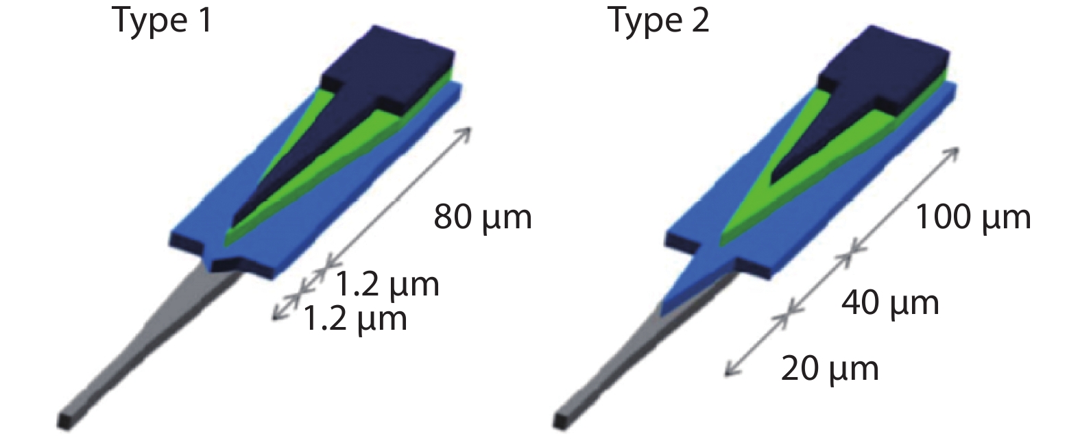
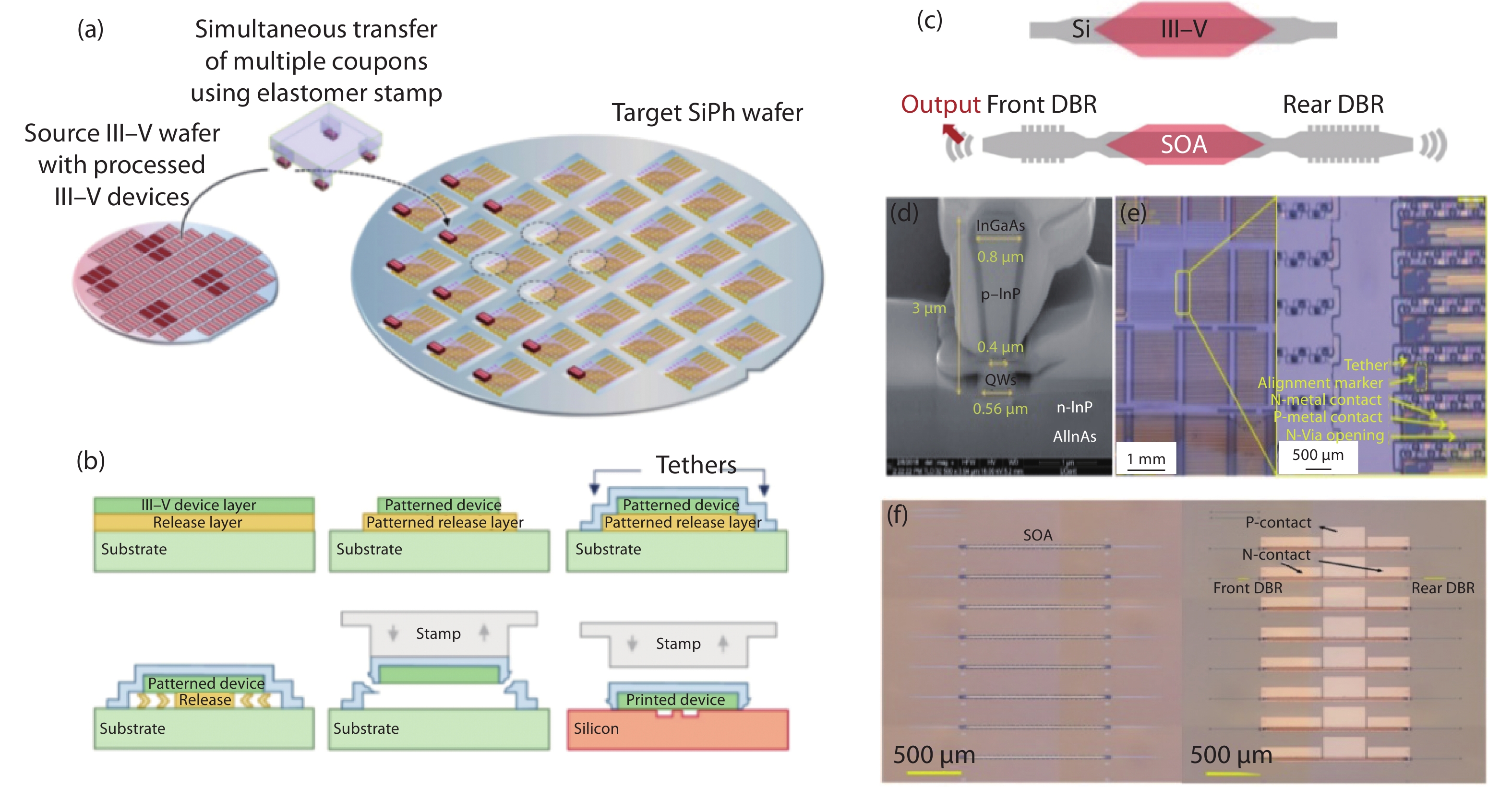
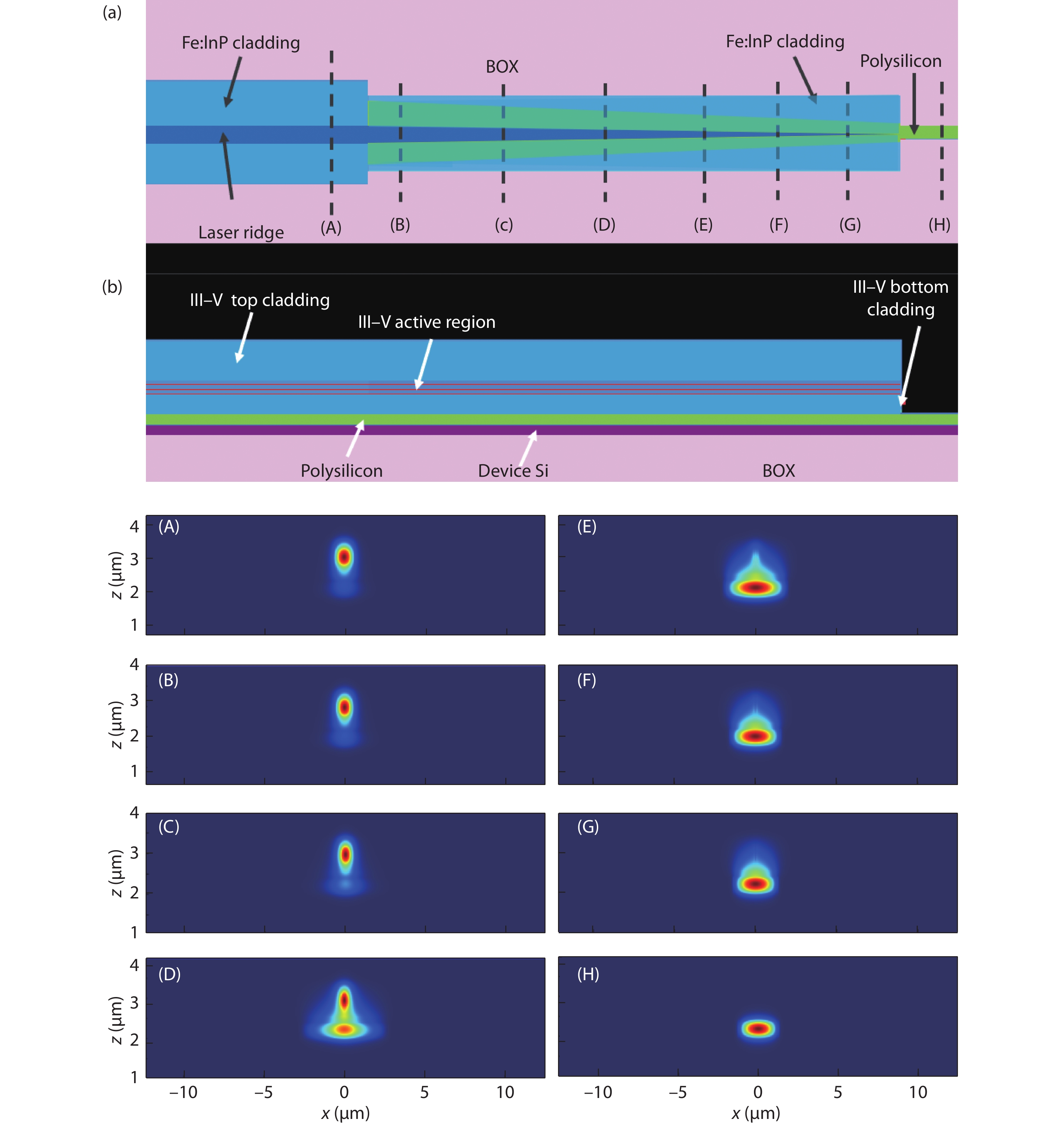
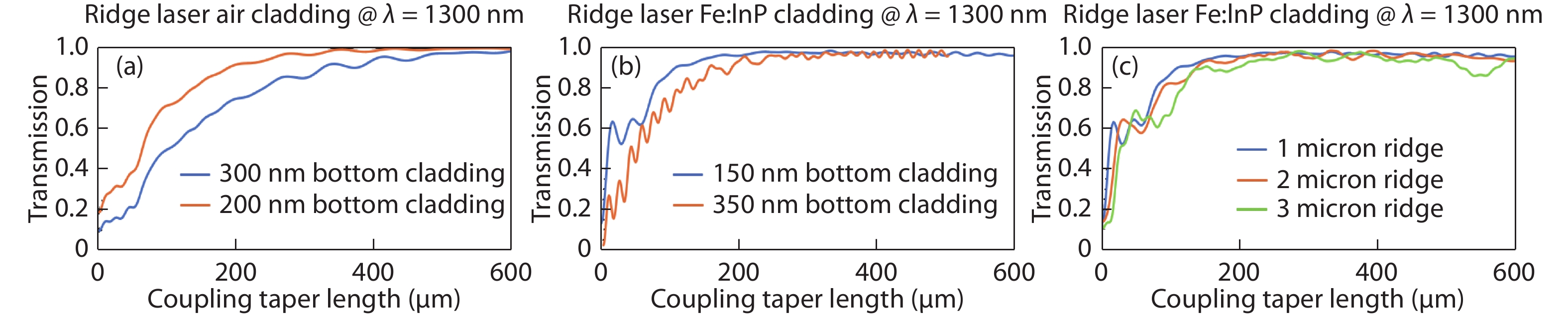
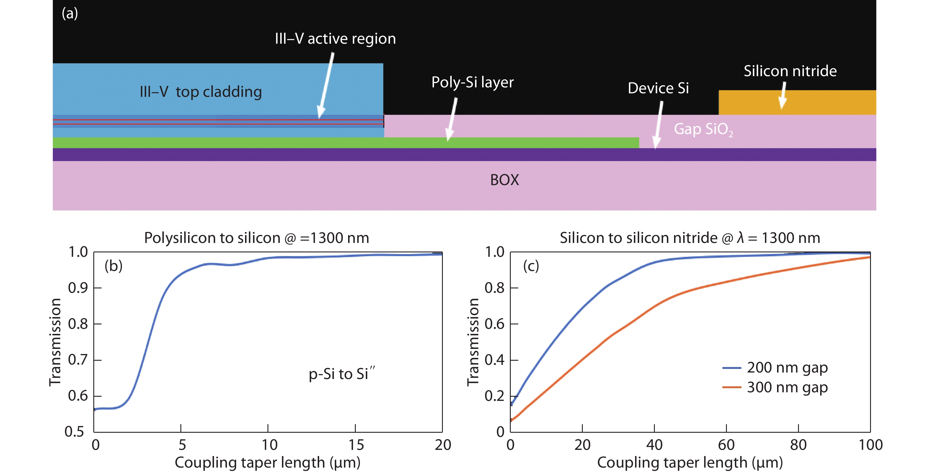
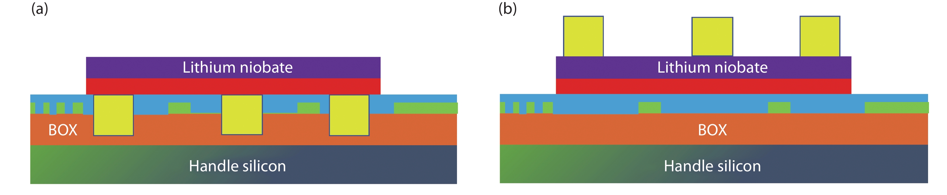
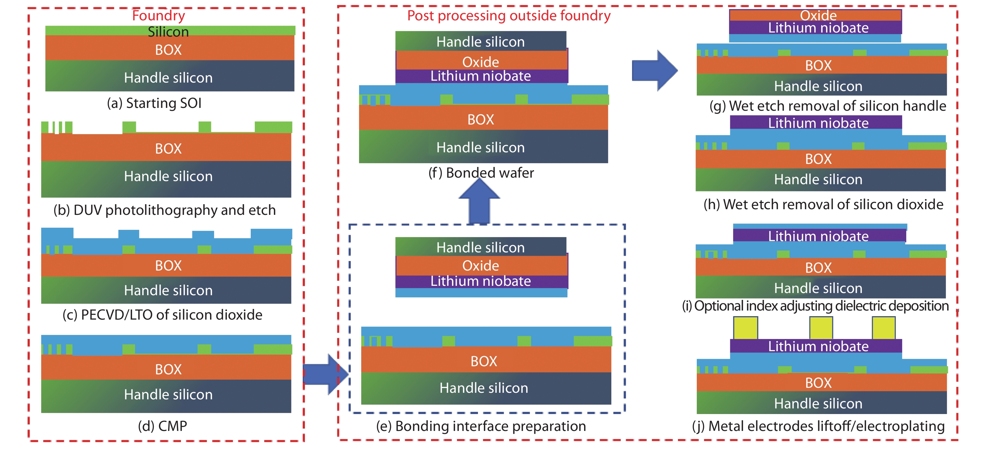
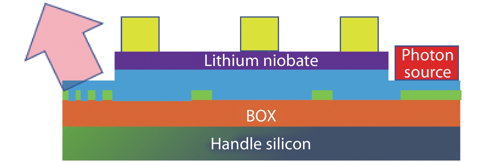
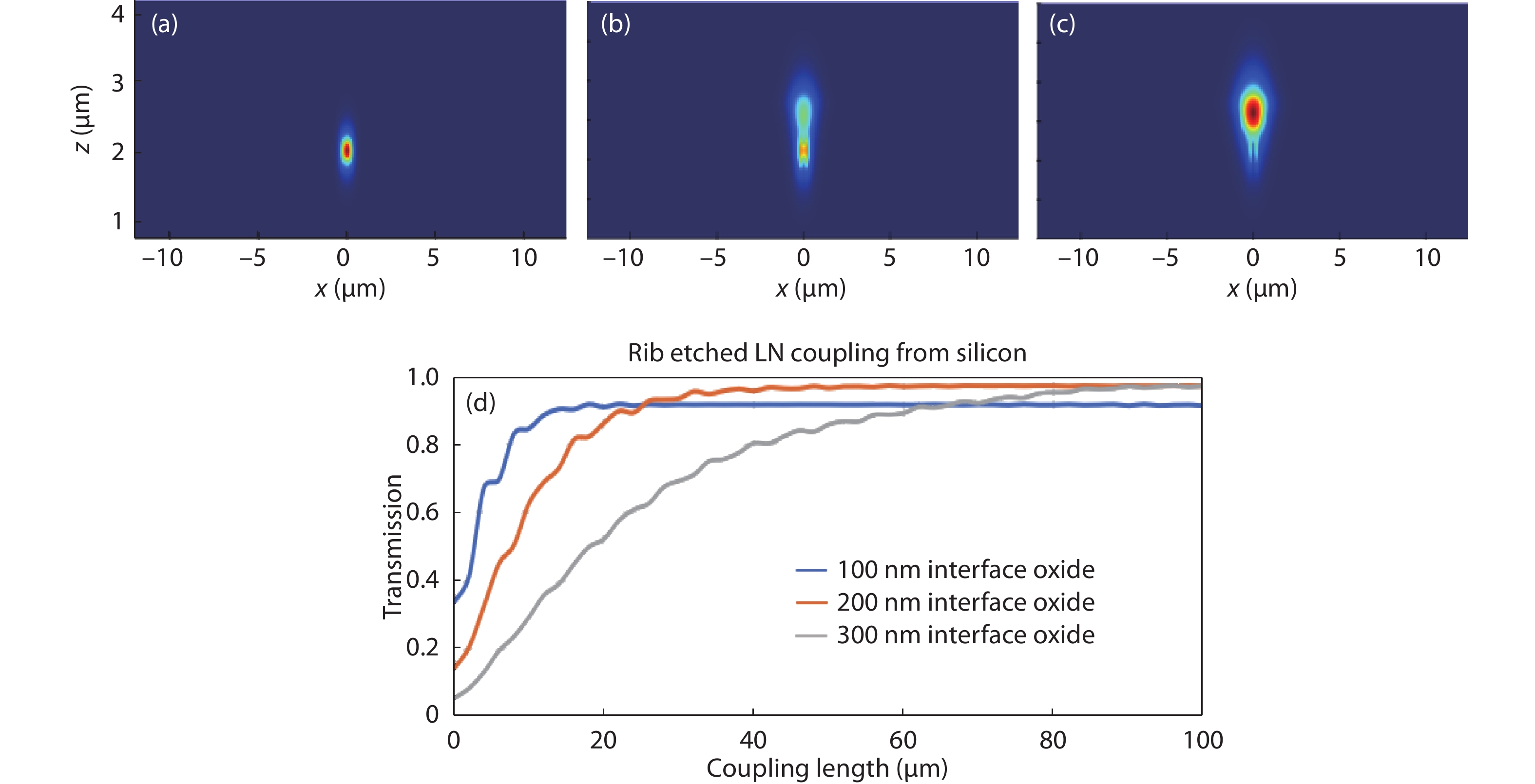
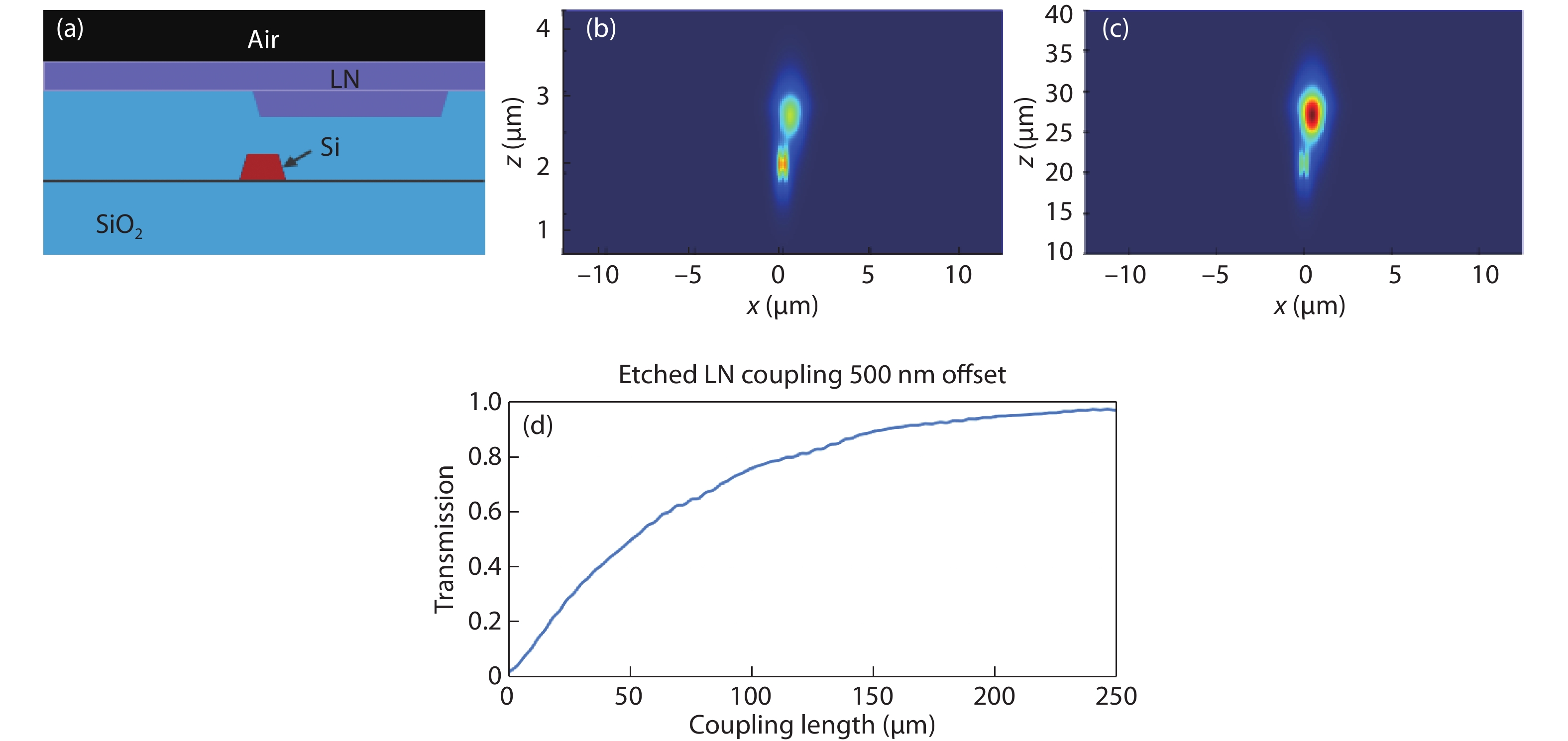
Hybrid integration of III–V and ferroelectric materials is being broadly adopted to enhance functionalities in silicon photonic integrated circuits (PICs). Bonding and transfer printing have been the popular approaches for integration of III–V gain media with silicon PICs. Similar approaches are also being considered for ferroelectrics to enable larger RF modulation bandwidths, higher linearity, lower optical loss integrated optical modulators on chip. In this paper, we review existing integration strategies of III–V materials and present a route towards hybrid integration of both III–V and ferroelectrics on the same chip. We show that adiabatic transformation of the optical mode between hybrid ferroelectric and silicon sections enables efficient transfer of optical modal energies for maximum overlap of the optical mode with the ferroelectric media, similar to approaches adopted to maximize optical overlap with the gain section, thereby reducing lasing thresholds for hybrid III–V integration with silicon PICs. Preliminary designs are presented to enable a foundry compatible hybrid integration route of diverse functionalities on silicon PICs.

Key words: CMOS technologyphotonic integrated circuitshybrid integrationferroelectric modulator


[1]
Doerr C R. Silicon photonic integration in telecommunications. Front Phys, 2015, 3, 37 doi: 10.3389/fphy.2015.00037
[2]
Xie W Q, Komljenovic T, Huang J X, et al. Heterogeneous silicon photonics sensing for autonomous cars. Opt Express, 2019, 27, 3642 doi: 10.1364/OE.27.003642
[3]
Marpaung D, Yao J P, Capmany J. Integrated microwave photonics. Nat Photonics, 2019, 13, 80 doi: 10.1002/lpor.201200032
[4]
Elshaari A W, Pernice W, Srinivasan K, et al. Hybrid integrated quantum photonic circuits. Nat Photonics, 2020, 14, 285 doi: 10.1038/s41566-020-0609-x
[5]
Liu L, van Campenhout J, Roelkens G, et al. Carrier-injection-based electro-optic modulator on silicon-on-insulator with a heterogeneously integrated III-V microdisk cavity. Opt Lett, 2008, 33, 2518 doi: 10.1364/OL.33.002518
[6]
Reed G T, Thomson D J, Gardes F Y, et al. High-speed carrier-depletion silicon Mach-Zehnder optical modulators with lateral PN junctions. Front Phys, 2014, 2, 77 doi: 10.3389/fphy.2014.00077
[7]
Debnath K, Thomson D J, Zhang W W, et al. All-silicon carrier accumulation modulator based on a lateral metal-oxide-semiconductor capacitor. Photonics Res, 2018, 6, 149 doi: 10.1364/PRJ.6.000149
[8]
Wang C, Zhang M, Chen X, et al. Integrated lithium niobate electro-optic modulators operating at CMOS-compatible voltages. Nature, 2018, 562, 101 doi: 10.1038/s41586-018-0551-y
[9]
Eltes F, Mai C, Caimi D, et al. A BaTiO3-based electro-optic pockels modulator monolithically integrated on an advanced silicon photonics platform. J Light Technol, 2019, 37, 1456 doi: 10.1109/JLT.2019.2893500
[10]
Wang X L, Lin C Y, Chakravarty S, et al. Effective in-device r33 of 735 pm/V on electro-optic polymer infiltrated silicon photonic crystal slot waveguides. Opt Lett, 2011, 36, 882 doi: 10.1364/OL.36.000882
[11]
Yariv A, Sun X K. Supermode Si/III-V hybrid lasers, optical amplifiers and modulators: A proposal and analysis. Opt Express, 2007, 15, 9147 doi: 10.1364/OE.15.009147
[12]
Tanaka S, Jeong S H, Sekiguchi S, et al. High-output-power, single-wavelength silicon hybrid laser using precise flip-chip bonding technology. Opt Express, 2012, 20, 28057 doi: 10.1364/OE.20.028057
[13]
Li Q, Lau K M. Epitaxial growth of highly mismatched III-V materials on (001) silicon for electronics and optoelectronics. Prog Cryst Growth Charact Mater, 2017, 63, 105 doi: 10.1016/j.pcrysgrow.2017.10.001
[14]
Roelkens G, Abassi A, Cardile P, et al. III-V-on-silicon photonic devices for optical communication and sensing. IEEE Photonics J, 2015, 3, 969 doi: 10.3390/photonics2030969
[15]
Roelkens G, van Thourhout D, Baets R, et al. Laser emission and photodetection in an InP/InGaAsP layer integrated on and coupled to a silicon-on-insulator waveguide circuit. Opt Express, 2006, 14, 8154 doi: 10.1364/OE.14.008154
[16]
Tatsumi T, Tanabe K, Watanabe K, et al. 1.3 μm InAs/GaAs quantum dot lasers on Si substrates by low-resistivity, Au-free metal-mediated wafer bonding. J Appl Phys, 2012, 112, 033107 doi: 10.1063/1.4742198
[17]
Hong T, Ran G Z, Chen T, et al. A selective-area metal bonding InGaAsP–Si laser. IEEE Photonics Technol Lett, 2010, 22, 1141 doi: 10.1109/LPT.2010.2050683
[18]
Liang D, Bowers J E. Highly efficient vertical outgassing channels for low-temperature InP-to-silicon direct wafer bonding on the silicon-on-insulator substrate. J Vac Sci Technol B, 2008, 26, 1560 doi: 10.1116/1.2943667
[19]
Zhang J, Muliuk G, Juvert J, et al. III-V-on-Si photonic integrated circuits realized using micro-transfer-printing. APL Photonics, 2019, 4, 110803 doi: 10.1063/1.5120004
[20]
de Beeck C O, Haq B, Elsinger L, et al. Heterogeneous III-V on silicon nitride amplifiers and lasers via microtransfer printing. Optica, 2020, 7, 386 doi: 10.1364/OPTICA.382989
[21]
Park H, Fang A, Kodama S, et al. Hybrid silicon evanescent laser fabricated with a silicon waveguide and III-V offset quantum wells. Opt Express, 2005, 13, 9460 doi: 10.1364/OPEX.13.009460
[22]
Kurczveil G, Pintus P, Heck M J R, et al. Characterization of insertion loss and back reflection in passive hybrid silicon tapers. IEEE Photonics J, 2013, 5, 6600410 doi: 10.1109/JPHOT.2013.2246559
[23]
Meitl M A, Zhu Z T, Kumar V, et al. Transfer printing by kinetic control of adhesion to an elastomeric stamp. Nat Mater, 2006, 5, 33 doi: 10.1038/nmat1532
[24]
Wang X X, Weigel P O, Zhao J, et al. Achieving beyond-100-GHz large-signal modulation bandwidth in hybrid silicon photonics Mach Zehnder modulators using thin film lithium niobate. APL Photonics, 2019, 4, 096101 doi: 10.1063/1.5115243
[25]
Tang Y, Peters J D, Bowers J E. Over 67 GHz bandwidth hybrid silicon electroabsorption modulator with asymmetric segmented electrode for 1.3 μm transmission. Opt Express, 2012, 20, 11529 doi: 10.1364/OE.20.011529
[26]
Menard E, Lee K J, Khang D Y, et al. A printable form of silicon for high performance thin film transistors on plastic substrates. Appl Phys Lett, 2004, 84, 5398 doi: 10.1063/1.1767591
[27]
Safian R, Teng M, Zhuang L M, et al. Foundry-compatible thin film lithium niobate modulator with RF electrodes buried inside the silicon oxide layer of the SOI wafer. Opt Express, 2020, 28, 25843 doi: 10.1364/OE.396335
[28]
Ayata M, Fedoryshyn Y, Heni W, et al. High-speed plasmonic modulator in a single metal layer. Science, 2017, 358, 630 doi: 10.1126/science.aan5953
[29]
Thomaschewski M, Zenin V A, Wolff C, et al. Plasmonic monolithic lithium niobate directional coupler switches. Nat Commun, 2020, 11, 1 doi: 10.1038/s41467-020-14539-y
Fig. 1.  (Color online) (a) Schematic of the hybrid laser with the superimposed optical mode. (b) SEM of cross-section of the hybrid laser[21, 22].

Fig. 2.  (Color online) Schematic of mode conversion tapers for coupling light into the silicon waveguide. The silicon waveguide is in gray while different sections of the top III –V layer with different taper lengths are shown in other colors[22].

Fig. 3.  (Color online) (a, b) Schematic Illustration of micro-transfer printing of III–V gain material on silicon wafers[19]. (c) Schematic integration and (d) SEM image of the III–V coupon with a silicon photonic waveguide. Top view microscope images of (e) large scale transfer printed coupons on a silicon photonic circuit, and (f) a semiconductor optical amplifier (SOA)[15].

Fig. 4.  (Color online) Schematic representation of the two supermodes, designated by Eo and Ee in the (left) lasing section (middle) coupling section and (right) passive waveguiding section[11].

Fig. 5.  (Color online) Schematic (a) top view and (b) side view of the III–V light emitting heterostructure with Fe:InP cladding in the buried heterostructure configuration integrated on a SOI wafer with an intermediate polysilicon layer (in green). A dual taper configuration is shown in the adiabatic mode transformation region where the laser ridge as well as the underlying polysilicon layers are tapered. The mode evolution of the fundamental TE mode from the gain region to the underlying silicon-poly-Si waveguide is shown in (A)–(H) with the corresponding cross-sections demarcated in (b).

Fig. 6.  (Color online) Coupling efficiency vs taper length as function of bottom cladding thickness for (a) air clad ridge laser and (b) buried heterostructure laser and (c) as a function of buried ridge width.

Fig. 7.  (Color online) (a) Schematic cross-section of the hybrid laser/light emitter bonded to polysilicon (in green) on device silicon (in purple). Coupling efficiency versus taper length for coupling from (b) poly-Si to 220 nm silicon, and (c) from 220 nm silicon to 400 nm silicon nitride for various oxide gaps between silicon and silicon nitride as indicated in (a).

Fig. 8.  (Color online) Reflectivity spectra of DBR reflectors for gratings with (a) etch depth of 100nm and 3600 periods with period Λ = 207 nm, (b) etch depth of 30nm and 7200 periods with Λ = 207 nm. (c) Vernier coupled ring spectra showing thermo-optic tuning around λ = 1295 nm.

Fig. 9.  (Color online) Schematic of hybrid TFLN integrated with silicon PICs with (a) embedded electrodes[26] and (b) un-embedded electrodes. Legend: (yellow) electrodes/metal contacts; (green) silicon or silicon nitride waveguides; (blue) silicon dioxide; (purple) thin film lithium niobate; (red) bonding interface with silicon dioxide between lithium niobate and top of silicon/silicon nitride waveguide.

Fig. 10.  (Color online) Steps in the hybrid integration of TFLN on silicon or silicon nitride PICs.

Fig. 11.  (Color online) Steps in the hybrid integration of a III–V laser with silicon in a hybrid TFLN on silicon or silicon nitride PIC.

Fig. 12.  (Color online) (a) Refractive index profile and (b) optical mode profile of the fundamental TE mode in a thin film ~400 nm LN bonded to a silicon waveguide 240 × 220 nm2 separated by 100 nm SiO2 interface. The top cladding is air.

Fig. 13.  (Color online) Tables indicating optical propagation loss contribution from the overlap of the propagating optical mode with the ground and signal electrodes as a function of interface oxide thickness (vertical axis) and spacing between ground and signal electrode (horizontal axis) for hybrid traveling wave modulator configuration with (a) an embedded electrode and (b) an un-embedded electrode.

Fig. 14.  (Color online) (a) Cross-section schematic of etched LN integrated with silicon PIC. (b) Optical propagation loss contribution from the overlap of the propagating optical mode with the ground and signal electrodes as a function of interface oxide thickness (vertical axis) and spacing between ground and signal electrode (horizontal axis) for hybrid traveling wave modulator configuration.

Fig. 15.  (Color online) Evolution of the optical mode as it couples from the silicon to the etched TFLN in Fig. 14(a) in (a) initially in silicon (b) adiabatic coupling section and (c) mode primarily in the TFLN in the modulator section. (d) Coupling efficiency as a function of adiabatic taper length for different thicknesses of the interface oxide.

Fig. 16.  (Color online) (a) Schematic cross-section assuming the TFLN slab has a misalignment offset of 500 nm perpendicular to the waveguide, when bonding. Mode profiles in the (b) adiabatic coupling section and (c) TFLN in the modulator section. (d) Coupling efficiency as a function of adiabatic taper length when waveguides are misaligned.

[1]
Doerr C R. Silicon photonic integration in telecommunications. Front Phys, 2015, 3, 37 doi: 10.3389/fphy.2015.00037
[2]
Xie W Q, Komljenovic T, Huang J X, et al. Heterogeneous silicon photonics sensing for autonomous cars. Opt Express, 2019, 27, 3642 doi: 10.1364/OE.27.003642
[3]
Marpaung D, Yao J P, Capmany J. Integrated microwave photonics. Nat Photonics, 2019, 13, 80 doi: 10.1002/lpor.201200032
[4]
Elshaari A W, Pernice W, Srinivasan K, et al. Hybrid integrated quantum photonic circuits. Nat Photonics, 2020, 14, 285 doi: 10.1038/s41566-020-0609-x
[5]
Liu L, van Campenhout J, Roelkens G, et al. Carrier-injection-based electro-optic modulator on silicon-on-insulator with a heterogeneously integrated III-V microdisk cavity. Opt Lett, 2008, 33, 2518 doi: 10.1364/OL.33.002518
[6]
Reed G T, Thomson D J, Gardes F Y, et al. High-speed carrier-depletion silicon Mach-Zehnder optical modulators with lateral PN junctions. Front Phys, 2014, 2, 77 doi: 10.3389/fphy.2014.00077
[7]
Debnath K, Thomson D J, Zhang W W, et al. All-silicon carrier accumulation modulator based on a lateral metal-oxide-semiconductor capacitor. Photonics Res, 2018, 6, 149 doi: 10.1364/PRJ.6.000149
[8]
Wang C, Zhang M, Chen X, et al. Integrated lithium niobate electro-optic modulators operating at CMOS-compatible voltages. Nature, 2018, 562, 101 doi: 10.1038/s41586-018-0551-y
[9]
Eltes F, Mai C, Caimi D, et al. A BaTiO3-based electro-optic pockels modulator monolithically integrated on an advanced silicon photonics platform. J Light Technol, 2019, 37, 1456 doi: 10.1109/JLT.2019.2893500
[10]
Wang X L, Lin C Y, Chakravarty S, et al. Effective in-device r33 of 735 pm/V on electro-optic polymer infiltrated silicon photonic crystal slot waveguides. Opt Lett, 2011, 36, 882 doi: 10.1364/OL.36.000882
[11]
Yariv A, Sun X K. Supermode Si/III-V hybrid lasers, optical amplifiers and modulators: A proposal and analysis. Opt Express, 2007, 15, 9147 doi: 10.1364/OE.15.009147
[12]
Tanaka S, Jeong S H, Sekiguchi S, et al. High-output-power, single-wavelength silicon hybrid laser using precise flip-chip bonding technology. Opt Express, 2012, 20, 28057 doi: 10.1364/OE.20.028057
[13]
Li Q, Lau K M. Epitaxial growth of highly mismatched III-V materials on (001) silicon for electronics and optoelectronics. Prog Cryst Growth Charact Mater, 2017, 63, 105 doi: 10.1016/j.pcrysgrow.2017.10.001
[14]
Roelkens G, Abassi A, Cardile P, et al. III-V-on-silicon photonic devices for optical communication and sensing. IEEE Photonics J, 2015, 3, 969 doi: 10.3390/photonics2030969
[15]
Roelkens G, van Thourhout D, Baets R, et al. Laser emission and photodetection in an InP/InGaAsP layer integrated on and coupled to a silicon-on-insulator waveguide circuit. Opt Express, 2006, 14, 8154 doi: 10.1364/OE.14.008154
[16]
Tatsumi T, Tanabe K, Watanabe K, et al. 1.3 μm InAs/GaAs quantum dot lasers on Si substrates by low-resistivity, Au-free metal-mediated wafer bonding. J Appl Phys, 2012, 112, 033107 doi: 10.1063/1.4742198
[17]
Hong T, Ran G Z, Chen T, et al. A selective-area metal bonding InGaAsP–Si laser. IEEE Photonics Technol Lett, 2010, 22, 1141 doi: 10.1109/LPT.2010.2050683
[18]
Liang D, Bowers J E. Highly efficient vertical outgassing channels for low-temperature InP-to-silicon direct wafer bonding on the silicon-on-insulator substrate. J Vac Sci Technol B, 2008, 26, 1560 doi: 10.1116/1.2943667
[19]
Zhang J, Muliuk G, Juvert J, et al. III-V-on-Si photonic integrated circuits realized using micro-transfer-printing. APL Photonics, 2019, 4, 110803 doi: 10.1063/1.5120004
[20]
de Beeck C O, Haq B, Elsinger L, et al. Heterogeneous III-V on silicon nitride amplifiers and lasers via microtransfer printing. Optica, 2020, 7, 386 doi: 10.1364/OPTICA.382989
[21]
Park H, Fang A, Kodama S, et al. Hybrid silicon evanescent laser fabricated with a silicon waveguide and III-V offset quantum wells. Opt Express, 2005, 13, 9460 doi: 10.1364/OPEX.13.009460
[22]
Kurczveil G, Pintus P, Heck M J R, et al. Characterization of insertion loss and back reflection in passive hybrid silicon tapers. IEEE Photonics J, 2013, 5, 6600410 doi: 10.1109/JPHOT.2013.2246559
[23]
Meitl M A, Zhu Z T, Kumar V, et al. Transfer printing by kinetic control of adhesion to an elastomeric stamp. Nat Mater, 2006, 5, 33 doi: 10.1038/nmat1532
[24]
Wang X X, Weigel P O, Zhao J, et al. Achieving beyond-100-GHz large-signal modulation bandwidth in hybrid silicon photonics Mach Zehnder modulators using thin film lithium niobate. APL Photonics, 2019, 4, 096101 doi: 10.1063/1.5115243
[25]
Tang Y, Peters J D, Bowers J E. Over 67 GHz bandwidth hybrid silicon electroabsorption modulator with asymmetric segmented electrode for 1.3 μm transmission. Opt Express, 2012, 20, 11529 doi: 10.1364/OE.20.011529
[26]
Menard E, Lee K J, Khang D Y, et al. A printable form of silicon for high performance thin film transistors on plastic substrates. Appl Phys Lett, 2004, 84, 5398 doi: 10.1063/1.1767591
[27]
Safian R, Teng M, Zhuang L M, et al. Foundry-compatible thin film lithium niobate modulator with RF electrodes buried inside the silicon oxide layer of the SOI wafer. Opt Express, 2020, 28, 25843 doi: 10.1364/OE.396335
[28]
Ayata M, Fedoryshyn Y, Heni W, et al. High-speed plasmonic modulator in a single metal layer. Science, 2017, 358, 630 doi: 10.1126/science.aan5953
[29]
Thomaschewski M, Zenin V A, Wolff C, et al. Plasmonic monolithic lithium niobate directional coupler switches. Nat Commun, 2020, 11, 1 doi: 10.1038/s41467-020-14539-y
  • Search

    Advanced Search >>

    GET CITATION

    shu

    Export: BibTex EndNote

    Article Metrics

    Article views: 3621 Times PDF downloads: 155 Times Cited by: 0 Times

    History

    Received: 26 October 2020 Revised: 05 December 2020 Online: Accepted Manuscript: 23 January 2021Uncorrected proof: 25 January 2021Published: 12 April 2021

    Catalog

      Email This Article

      User name:
      Email:*请输入正确邮箱
      Code:*验证码错误
      Swapnajit Chakravarty, Min Teng, Reza Safian, Leimeng Zhuang. Hybrid material integration in silicon photonic integrated circuits[J]. Journal of Semiconductors, 2021, 42(4): 041303. doi: 10.1088/1674-4926/42/4/041303 S Chakravarty, M Teng, R Safian, L M Zhuang, Hybrid material integration in silicon photonic integrated circuits[J]. J. Semicond., 2021, 42(4): 041303. doi: 10.1088/1674-4926/42/4/041303.Export: BibTex EndNote
      Citation:
      Swapnajit Chakravarty, Min Teng, Reza Safian, Leimeng Zhuang. Hybrid material integration in silicon photonic integrated circuits[J]. Journal of Semiconductors, 2021, 42(4): 041303. doi: 10.1088/1674-4926/42/4/041303

      S Chakravarty, M Teng, R Safian, L M Zhuang, Hybrid material integration in silicon photonic integrated circuits[J]. J. Semicond., 2021, 42(4): 041303. doi: 10.1088/1674-4926/42/4/041303.
      Export: BibTex EndNote

      Hybrid material integration in silicon photonic integrated circuits

      doi: 10.1088/1674-4926/42/4/041303
      More Information
      • Author Bio:

        Swapnajit Chakravarty is Principal Researcher at IMEC USA. He received his PhD in Electrical Engineering from the University of Michigan, Ann Arbor. His research focuses on silicon, III-V, and ferroelectrics for monolithic and hybrid PICs for chem-bio sensors and devices for optical communications. Dr. Chakravarty has 15 issued patents, 47 journal papers, 85 conference papers, 7 invited talks. He is a Senior Member of IEEE, SPIE, and OSA

        Min Teng Received his Ph.D. degree in Electrical and Computer Engineering from Purdue University, in 2018. He worked at Mitsubishi Electric Research Laboratory in 2017. In 2018, He joined Imec USA nanoeletronics design center, where he is working on photonic integrated circuit design. He is coauthor of 15 journal papers, conference proceedings and patents

        Reza Safian received his M.Sc degree in electrical engineering from McMaster University in 2003, and the Ph.D degree in electrical engineering from the University of Toronto in 2008. He joined the faculty of the department of electrical and computer engineering at Isfahan university of technology in 2008 where he was involved in the field of terahertz and millimeter wave imaging and microwave photonics. He was a visiting researcher in Center for Research and Education in Optics and Lasers (CREOL) in university of central Florida in 2017, working on wideband integrated electro-optic modulators. In 2018, he joined the Imec R&D, nano electronics and digital technologies in Florida, where he is working in the field of photonic integrated circuits for coherent optical transceivers. He is the author or coauthor of more than 100 papers in journals and conference proceedings

        Leimeng Zhuang received his Ph.D. degree in electrical engineering, from the Univeristy of Twente, Enschede, The Netherlands, in 2010. From 2010 until 2013, he worked as a Research Fellow at the University of Twente, LioniX International, and Dutch National Aerospace Laboratory, responsible for the development of a satellite tracking phased array antenna system. From 2014 until 2018, as Senior Research Fellow/Senior Lecture, he worked at the Electro-Photonics Laboratory, Electrical and Computer Systems Engineering, Monash University in Melbourne, Australia, leading the research topic of hybrid electronics-photonics signal processing for high-speed, energy-efficient optical communication systems and microwave photonics. In September 2018, he joined imec USA, Nanocenter for high-speed electronics and photonics. He is currently leading the Photonics Team for R&D projects on silicon photonics technology including coherent optical transceivers, LIDAR, photonics AI, and high-speed modulators using E-O materials

      • Corresponding author: swapnajit.chakravarty@imec-int.com
      • Received Date: 2020-10-26
      • Revised Date: 2020-12-05
      • Published Date: 2021-04-10

      Catalog

        /

        DownLoad:  Full-Size Img  PowerPoint
        Return
        Return