


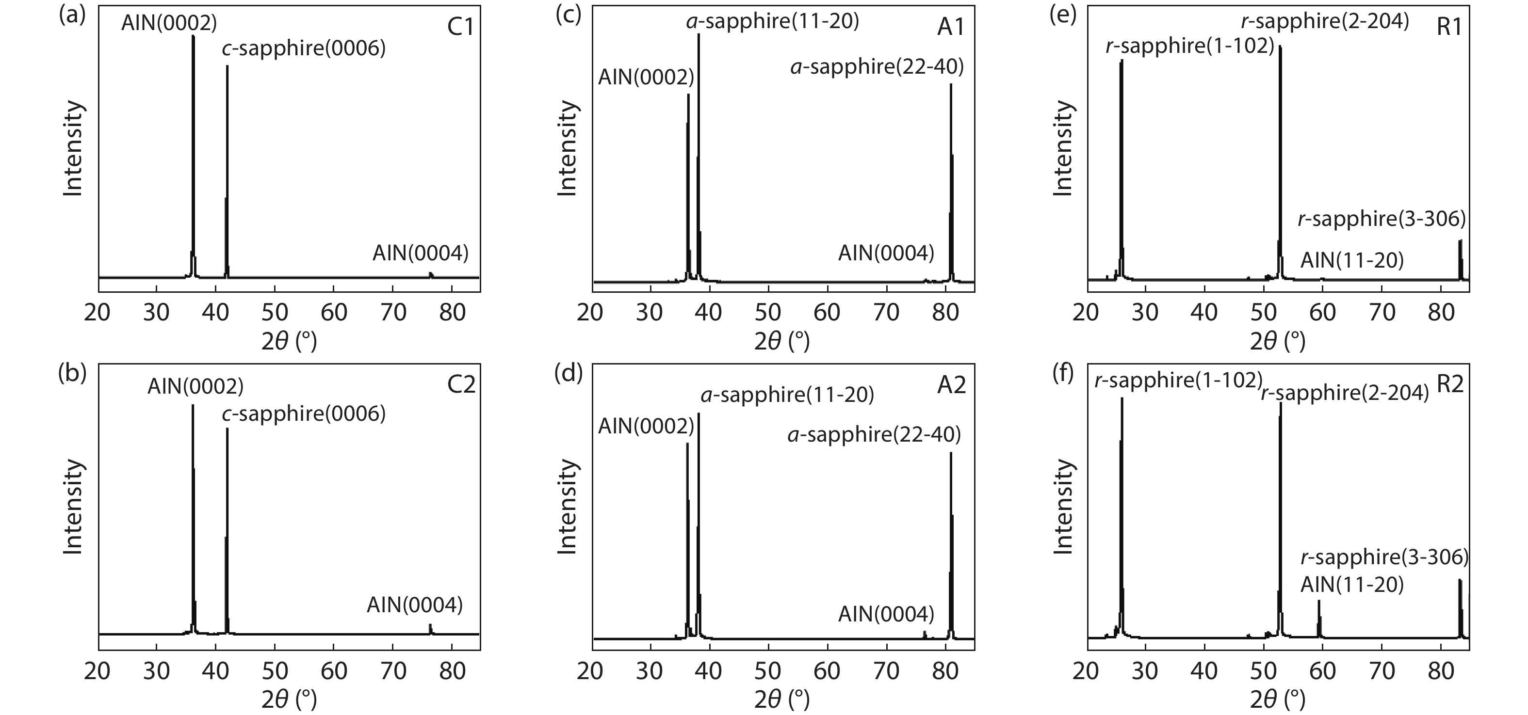
Fig. 1.
Powder X-ray diffraction spectra of AlN deposited on (a, b) c , (c, d) a and (e, f) r-plane sapphire substrates before and after thermal annealing. Clear diffraction peaks from AlN and sapphire can be identified.
ARTICLES
Xianchun Peng1, 2, Jie Sun1, Huan Liu3, 4, Liang Li1, Qikun Wang4, Liang Wu4, Wei Guo1, , Fanping Meng1, , Li Chen1, Feng Huang1 and Jichun Ye1,
Corresponding author: Wei Guo, guowei@nimte.ac.cn; Fanping Meng, mengfp@nimte.ac.cn; Jichun Ye, jichun.ye@nimte.ac.cn
Abstract: AlN thin films were deposited on c-, a- and r-plane sapphire substrates by the magnetron sputtering technique. The influence of high-temperature thermal annealing (HTTA) on the structural, optical properties as well as surface stoichiometry were comprehensively investigated. The significant narrowing of the (0002) diffraction peak to as low as 68 arcsec of AlN after HTTA implies a reduction of tilt component inside the AlN thin films, and consequently much-reduced dislocation densities. This is also supported by the appearance of E2(high) Raman peak and better Al–N stoichiometry after HTTA. Furthermore, the increased absorption edge after HTTA suggests a reduction of point defects acting as the absorption centers. It is concluded that HTTA is a universal post-treatment technique in improving the crystalline quality of sputtered AlN regardless of sapphire orientation.
Key words: nitrides, physical vapor deposition processes, semiconducting III–V materials, defects
| [1] |
Taniyasu Y, Kasu M, Makimoto T. An aluminium nitride light-emitting diode with a wavelength of 210 nanometres. Nature, 2006, 441, 325 doi: 10.1038/nature04760
|
| [2] |
Hartmann C, Wollweber J, Dittmar A, et al. Preparation of bulk AlN seeds by spontaneous nucleation of freestanding crystals. Jpn J Appl Phys, 2013, 52, 08JA06 doi: 10.7567/JJAP.52.08JA06
|
| [3] |
Nagahama S I, Iwasa N, Senoh M, et al. High-power and long-lifetime InGaN multi-quantum-well laser diodes grown on low-dislocation-density GaN substrates. Jpn J Appl Phys, 2000, 39, L647 doi: 10.1143/JJAP.39.L647
|
| [4] |
Asif Khan M, Shatalov M, Maruska H P, et al. III–nitride UV devices. Jpn J Appl Phys, 2005, 44, 7191 doi: 10.1143/JJAP.44.7191
|
| [5] |
Hirayama H, Noguchi N, Fujikawa S, et al. 222–282 nm AlGaN and InAlGaN based deep-UV LEDs fabricated on high-quality AlN template. Proc SPIE 7216, Gallium Nitride Materials and Devices IV, 2009, 7216, 721621 doi: 10.1117/12.809729
|
| [6] |
Xu H Q, Jiang J A, Chen L, et al. Direct demonstration of carrier distribution and recombination within step-bunched UV-LEDs. Photon Res, 2021, 9, 764 doi: 10.1364/PRJ.411832
|
| [7] |
Sun H D, Mitra S, Subedi R C, et al. Unambiguously enhanced ultraviolet luminescence of AlGaN wavy quantum well structures grown on large misoriented sapphire substrate. Adv Funct Mater, 2019, 29, 1905445 doi: 10.1002/adfm.201905445
|
| [8] |
Kneissl M, Seong T Y, Han J, et al. The emergence and prospects of deep-ultraviolet light-emitting diode technologies. Nat Photonics, 2019, 13, 233 doi: 10.1038/s41566-019-0359-9
|
| [9] |
Xu H, Long H, Jiang J, et al. Strain modulated nanostructure patterned AlGaN-based deep ultraviolet multiple-quantum-wells for polarization control and light extraction efficiency enhancement. Nanotechnology, 2019, 30, 435202 doi: 10.1088/1361-6528/ab3208
|
| [10] |
Fu H Q, Baranowski I, Huang X Q, et al. Demonstration of AlN Schottky barrier diodes with blocking voltage over 1 kV. IEEE Electron Device Lett, 2017, 38, 1286 doi: 10.1109/LED.2017.2723603
|
| [11] |
Damjanovic D. Materials for high temperature piezoelectric transducers. Curr Opin Solid State Mater Sci, 1998, 3, 469 doi: 10.1016/S1359-0286(98)80009-0
|
| [12] |
Iriarte G F. Influence of the magnetron on the growth of aluminum nitride thin films deposited by reactive sputtering. J Vac Sci Technol A, 2010, 28, 193 doi: 10.1116/1.3280174
|
| [13] |
Miyake H, Lin C H, Tokoro K, et al. Preparation of high-quality AlN on sapphire by high-temperature face-to-face annealing. J Cryst Growth, 2016, 456, 155 doi: 10.1016/j.jcrysgro.2016.08.028
|
| [14] |
Guo J, Wang H Y, Meng F P, et al. Tuning the H/E* ratio and E* of AlN coatings by copper addition. Surf Coat Technol, 2013, 228, 68 doi: 10.1016/j.surfcoat.2013.04.008
|
| [15] |
Ben J W, Sun X J, Jia Y P, et al. Defect evolution in AlN templates on PVD-AlN/sapphire substrates by thermal annealing. CrystEngComm, 2018, 20, 4623 doi: 10.1039/C8CE00770E
|
| [16] |
Hagedorn S, Walde S, Mogilatenko A, et al. Stabilization of sputtered AlN/sapphire templates during high temperature annealing. J Cryst Growth, 2019, 512, 142 doi: 10.1016/j.jcrysgro.2019.02.024
|
| [17] |
Chen L, Lin W, Chen H Y, et al. Annihilation and regeneration of defects in (112̅2) semipolar AlN via high-temperature annealing and MOVPE regrowth. Cryst Growth Des, 2021, 21, 2911 doi: 10.1021/acs.cgd.1c00086
|
| [18] |
Xiao S Y, Suzuki R, Miyake H, et al. Improvement mechanism of sputtered AlN films by high-temperature annealing. J Cryst Growth, 2018, 502, 41 doi: 10.1016/j.jcrysgro.2018.09.002
|
| [19] |
Huang C Y, Wu P Y, Chang K S, et al. High-quality and highly-transparent AlN template on annealed sputter-deposited AlN buffer layer for deep ultra-violet light-emitting diodes. AIP Adv, 2017, 7, 055110 doi: 10.1063/1.4983708
|
| [20] |
Guo W, Mitra S, Jiang J, et al. Three-dimensional band diagram in lateral polarity junction III-nitride heterostructures. Optica, 2019, 6, 1058 doi: 10.1364/OPTICA.6.001058
|
| [21] |
Yan L, Zhang Y T, Han X, et al. Polarization-induced hole doping in N-polar III-nitride LED grown by metalorganic chemical vapor deposition. Appl Phys Lett, 2018, 112, 182104 doi: 10.1063/1.5023521
|
| [22] |
Meng F P, Wang B, Ge F F, et al. Microstructure and mechanical properties of Ni-alloyed SiC coatings. Surf Coat Technol, 2012, 213, 77 doi: 10.1016/j.surfcoat.2012.10.020
|
| [23] |
Huang F, Ge F F, Zhu P, et al. Superhard V-Si-N coatings (>50GPa) with the cell-like nanostructure prepared by magnetron sputtering. Surf Coat Technol, 2013, 232, 600 doi: 10.1016/j.surfcoat.2013.06.035
|
| [24] |
Jose F, Ramaseshan R, Dash S, et al. Response of magnetron sputtered AlN films to controlled atmosphere annealing. J Phys D, 2010, 43, 075304 doi: 10.1088/0022-3727/43/7/075304
|
| [25] |
Iriarte G F, Reyes D F, González D, et al. Influence of substrate crystallography on the room temperature synthesis of AlN thin films by reactive sputtering. Appl Surf Sci, 2011, 257, 9306 doi: 10.1016/j.apsusc.2011.05.025
|
| [26] |
Ban K, Yamamoto J I, Takeda K, et al. Internal quantum efficiency of whole-composition-range AlGaN multiquantum wells. Appl Phys Express, 2011, 4, 052101 doi: 10.1143/APEX.4.052101
|
| [27] |
Demir I, Li H, Robin Y, et al. Sandwich method to grow high quality AlN by MOCVD. J Phys D, 2018, 51, 085104 doi: 10.1088/1361-6463/aaa926
|
| [28] |
Yoshikawa A, Nagatomi T, Morishita T, et al. High-quality AlN film grown on a nanosized concave-convex surface sapphire substrate by metalorganic vapor phase epitaxy. Appl Phys Lett, 2017, 111, 162102 doi: 10.1063/1.5008258
|
| [29] |
Ben J W, Shi Z M, Zang H, et al. The formation mechanism of voids in physical vapor deposited AlN epilayer during high temperature annealing. Appl Phys Lett, 2020, 116, 251601 doi: 10.1063/5.0012792
|
| [30] |
Moram M A, Johnston C F, Hollander J L, et al. Understanding X-ray diffraction of nonpolar gallium nitride films. J Appl Phys, 2009, 105, 113501 doi: 10.1063/1.3129307
|
| [31] |
Uedono A, Shojiki K, Uesugi K, et al. Annealing behaviors of vacancy-type defects in AlN deposited by radio-frequency sputtering and metalorganic vapor phase epitaxy studied using monoenergetic positron beams. J Appl Phys, 2020, 128, 085704 doi: 10.1063/5.0015225
|
| [32] |
Uesugi K, Hayashi Y, Shojiki K, et al. Reduction of threading dislocation density and suppression of cracking in sputter-deposited AlN templates annealed at high temperatures. Appl Phys Express, 2019, 12, 065501 doi: 10.7567/1882-0786/ab1ab8
|
| [33] |
Gaddy B E, Bryan Z, Bryan I, et al. Vacancy compensation and related donor-acceptor pair recombination in bulk AlN. Appl Phys Lett, 2013, 103, 161901 doi: 10.1063/1.4824731
|
| [34] |
Venkatachalam S, Mangalaraj D, Narayandass S K, et al. Structure, optical and electrical properties of ZnSe thin films. Phys B, 2005, 358, 27 doi: 10.1016/j.physb.2004.12.022
|
| [35] |
Silveira E, Freitas J A, Schujman S B, et al. AlN bandgap temperature dependence from its optical properties. J Cryst Growth, 2008, 310, 4007 doi: 10.1016/j.jcrysgro.2008.06.015
|
| [36] |
Alden D, Harris J S, Bryan Z, et al. Point-defect nature of the ultraviolet absorption band in AlN. Phys Rev Appl, 2018, 9, 054036 doi: 10.1103/PhysRevApplied.9.054036
|
| [37] |
Chen S, Zhang X, Wang S C, et al. High quality non-polar a-plane AlN template grown on semi-polar r-plane sapphire substrate by three-step pulsed flow growth method. J Alloys Compd, 2021, 872, 159706 doi: 10.1016/j.jallcom.2021.159706
|
| [38] |
Kirste R, Mita S, Hussey L, et al. Polarity control and growth of lateral polarity structures in AlN. Appl Phys Lett, 2013, 102, 181913 doi: 10.1063/1.4804575
|
| [39] |
Sharma N, Ilango S, Dash S, et al. X-ray photoelectron spectroscopy studies on AlN thin films grown by ion beam sputtering in reactive assistance of N+/N2+ ions: Substrate temperature induced compositional variations. Thin Solid Films, 2017, 636, 626 doi: 10.1016/j.tsf.2017.07.006
|
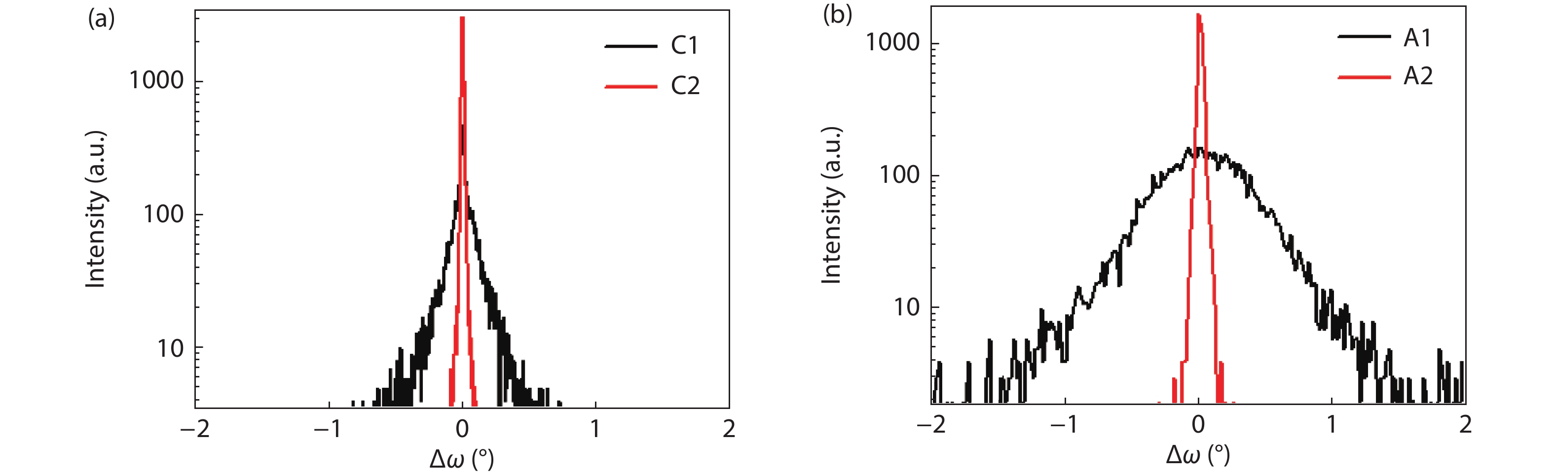
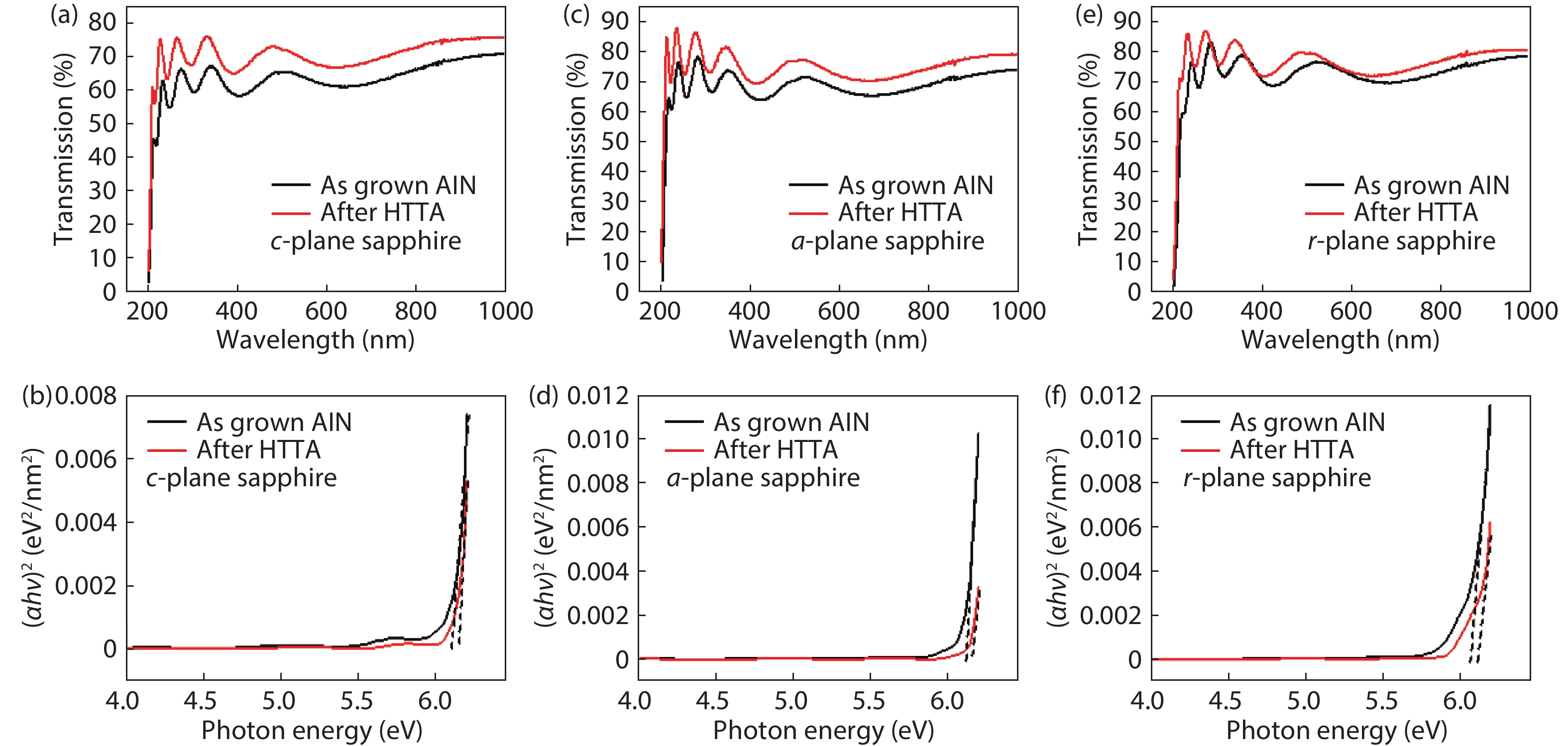

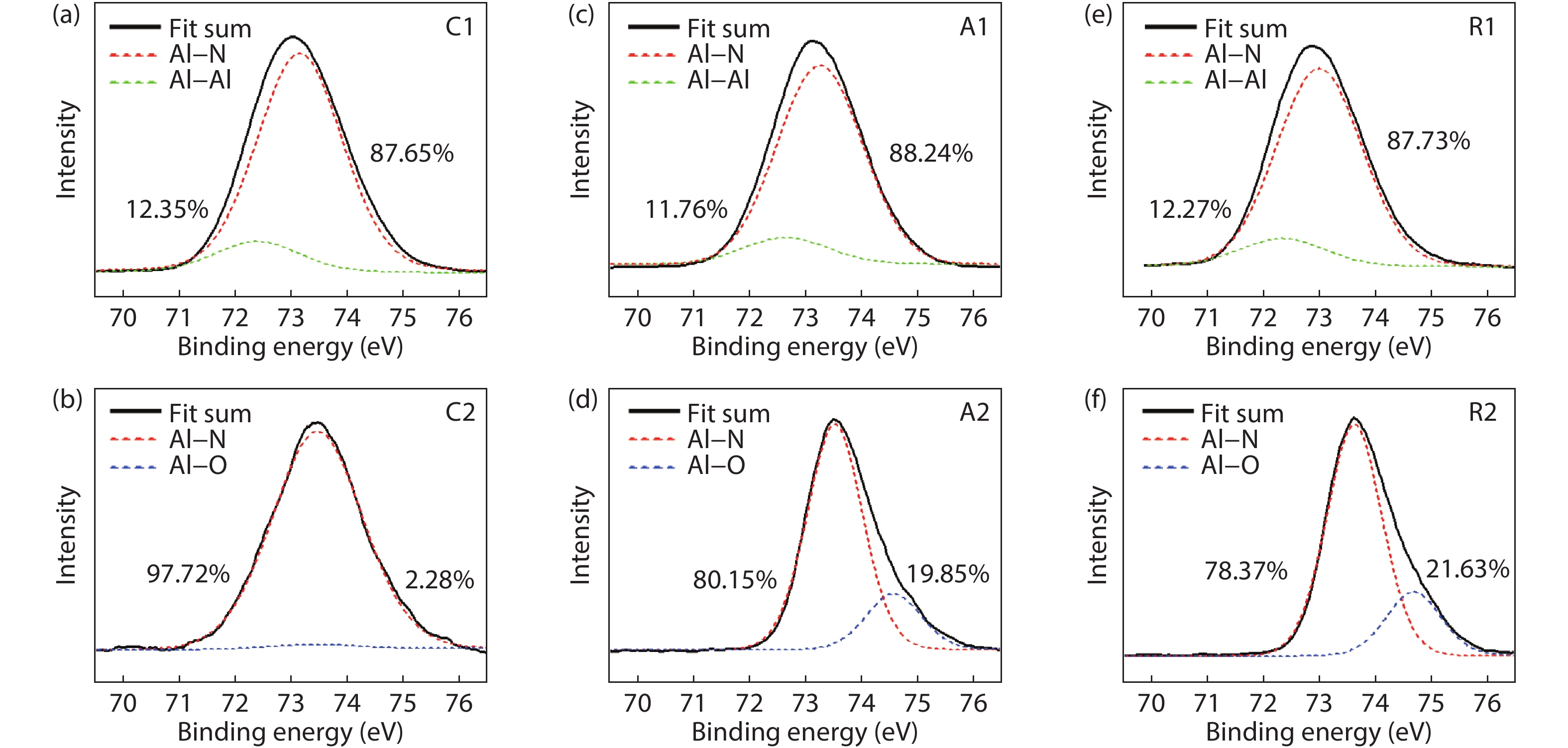
Table 1. Calculated absorption edges of AlN thin films acquired by α2 versus photon energy curve, rms roughness and the FWHM of the (002) diffraction peaks.
| Sapphire orientation | Band gap (eV) | RMS (nm) | Peak FWHM (arcsec) | |
| c-plane | C1 | 6.107 | 1.66 | 252 |
| C2 | 6.114 | 2.03 | 68 | |
| a-plane | A1 | 6.109 | 2.86 | 2494 |
| A2 | 6.126 | 0.717 | 151 | |
| r-plane | R1 | 6.069 | 5.15 | – |
| R2 | 6.081 | 6.11 | – | |
 DownLoad: CSV
| [1] |
Taniyasu Y, Kasu M, Makimoto T. An aluminium nitride light-emitting diode with a wavelength of 210 nanometres. Nature, 2006, 441, 325 doi: 10.1038/nature04760
|
| [2] |
Hartmann C, Wollweber J, Dittmar A, et al. Preparation of bulk AlN seeds by spontaneous nucleation of freestanding crystals. Jpn J Appl Phys, 2013, 52, 08JA06 doi: 10.7567/JJAP.52.08JA06
|
| [3] |
Nagahama S I, Iwasa N, Senoh M, et al. High-power and long-lifetime InGaN multi-quantum-well laser diodes grown on low-dislocation-density GaN substrates. Jpn J Appl Phys, 2000, 39, L647 doi: 10.1143/JJAP.39.L647
|
| [4] |
Asif Khan M, Shatalov M, Maruska H P, et al. III–nitride UV devices. Jpn J Appl Phys, 2005, 44, 7191 doi: 10.1143/JJAP.44.7191
|
| [5] |
Hirayama H, Noguchi N, Fujikawa S, et al. 222–282 nm AlGaN and InAlGaN based deep-UV LEDs fabricated on high-quality AlN template. Proc SPIE 7216, Gallium Nitride Materials and Devices IV, 2009, 7216, 721621 doi: 10.1117/12.809729
|
| [6] |
Xu H Q, Jiang J A, Chen L, et al. Direct demonstration of carrier distribution and recombination within step-bunched UV-LEDs. Photon Res, 2021, 9, 764 doi: 10.1364/PRJ.411832
|
| [7] |
Sun H D, Mitra S, Subedi R C, et al. Unambiguously enhanced ultraviolet luminescence of AlGaN wavy quantum well structures grown on large misoriented sapphire substrate. Adv Funct Mater, 2019, 29, 1905445 doi: 10.1002/adfm.201905445
|
| [8] |
Kneissl M, Seong T Y, Han J, et al. The emergence and prospects of deep-ultraviolet light-emitting diode technologies. Nat Photonics, 2019, 13, 233 doi: 10.1038/s41566-019-0359-9
|
| [9] |
Xu H, Long H, Jiang J, et al. Strain modulated nanostructure patterned AlGaN-based deep ultraviolet multiple-quantum-wells for polarization control and light extraction efficiency enhancement. Nanotechnology, 2019, 30, 435202 doi: 10.1088/1361-6528/ab3208
|
| [10] |
Fu H Q, Baranowski I, Huang X Q, et al. Demonstration of AlN Schottky barrier diodes with blocking voltage over 1 kV. IEEE Electron Device Lett, 2017, 38, 1286 doi: 10.1109/LED.2017.2723603
|
| [11] |
Damjanovic D. Materials for high temperature piezoelectric transducers. Curr Opin Solid State Mater Sci, 1998, 3, 469 doi: 10.1016/S1359-0286(98)80009-0
|
| [12] |
Iriarte G F. Influence of the magnetron on the growth of aluminum nitride thin films deposited by reactive sputtering. J Vac Sci Technol A, 2010, 28, 193 doi: 10.1116/1.3280174
|
| [13] |
Miyake H, Lin C H, Tokoro K, et al. Preparation of high-quality AlN on sapphire by high-temperature face-to-face annealing. J Cryst Growth, 2016, 456, 155 doi: 10.1016/j.jcrysgro.2016.08.028
|
| [14] |
Guo J, Wang H Y, Meng F P, et al. Tuning the H/E* ratio and E* of AlN coatings by copper addition. Surf Coat Technol, 2013, 228, 68 doi: 10.1016/j.surfcoat.2013.04.008
|
| [15] |
Ben J W, Sun X J, Jia Y P, et al. Defect evolution in AlN templates on PVD-AlN/sapphire substrates by thermal annealing. CrystEngComm, 2018, 20, 4623 doi: 10.1039/C8CE00770E
|
| [16] |
Hagedorn S, Walde S, Mogilatenko A, et al. Stabilization of sputtered AlN/sapphire templates during high temperature annealing. J Cryst Growth, 2019, 512, 142 doi: 10.1016/j.jcrysgro.2019.02.024
|
| [17] |
Chen L, Lin W, Chen H Y, et al. Annihilation and regeneration of defects in (112̅2) semipolar AlN via high-temperature annealing and MOVPE regrowth. Cryst Growth Des, 2021, 21, 2911 doi: 10.1021/acs.cgd.1c00086
|
| [18] |
Xiao S Y, Suzuki R, Miyake H, et al. Improvement mechanism of sputtered AlN films by high-temperature annealing. J Cryst Growth, 2018, 502, 41 doi: 10.1016/j.jcrysgro.2018.09.002
|
| [19] |
Huang C Y, Wu P Y, Chang K S, et al. High-quality and highly-transparent AlN template on annealed sputter-deposited AlN buffer layer for deep ultra-violet light-emitting diodes. AIP Adv, 2017, 7, 055110 doi: 10.1063/1.4983708
|
| [20] |
Guo W, Mitra S, Jiang J, et al. Three-dimensional band diagram in lateral polarity junction III-nitride heterostructures. Optica, 2019, 6, 1058 doi: 10.1364/OPTICA.6.001058
|
| [21] |
Yan L, Zhang Y T, Han X, et al. Polarization-induced hole doping in N-polar III-nitride LED grown by metalorganic chemical vapor deposition. Appl Phys Lett, 2018, 112, 182104 doi: 10.1063/1.5023521
|
| [22] |
Meng F P, Wang B, Ge F F, et al. Microstructure and mechanical properties of Ni-alloyed SiC coatings. Surf Coat Technol, 2012, 213, 77 doi: 10.1016/j.surfcoat.2012.10.020
|
| [23] |
Huang F, Ge F F, Zhu P, et al. Superhard V-Si-N coatings (>50GPa) with the cell-like nanostructure prepared by magnetron sputtering. Surf Coat Technol, 2013, 232, 600 doi: 10.1016/j.surfcoat.2013.06.035
|
| [24] |
Jose F, Ramaseshan R, Dash S, et al. Response of magnetron sputtered AlN films to controlled atmosphere annealing. J Phys D, 2010, 43, 075304 doi: 10.1088/0022-3727/43/7/075304
|
| [25] |
Iriarte G F, Reyes D F, González D, et al. Influence of substrate crystallography on the room temperature synthesis of AlN thin films by reactive sputtering. Appl Surf Sci, 2011, 257, 9306 doi: 10.1016/j.apsusc.2011.05.025
|
| [26] |
Ban K, Yamamoto J I, Takeda K, et al. Internal quantum efficiency of whole-composition-range AlGaN multiquantum wells. Appl Phys Express, 2011, 4, 052101 doi: 10.1143/APEX.4.052101
|
| [27] |
Demir I, Li H, Robin Y, et al. Sandwich method to grow high quality AlN by MOCVD. J Phys D, 2018, 51, 085104 doi: 10.1088/1361-6463/aaa926
|
| [28] |
Yoshikawa A, Nagatomi T, Morishita T, et al. High-quality AlN film grown on a nanosized concave-convex surface sapphire substrate by metalorganic vapor phase epitaxy. Appl Phys Lett, 2017, 111, 162102 doi: 10.1063/1.5008258
|
| [29] |
Ben J W, Shi Z M, Zang H, et al. The formation mechanism of voids in physical vapor deposited AlN epilayer during high temperature annealing. Appl Phys Lett, 2020, 116, 251601 doi: 10.1063/5.0012792
|
| [30] |
Moram M A, Johnston C F, Hollander J L, et al. Understanding X-ray diffraction of nonpolar gallium nitride films. J Appl Phys, 2009, 105, 113501 doi: 10.1063/1.3129307
|
| [31] |
Uedono A, Shojiki K, Uesugi K, et al. Annealing behaviors of vacancy-type defects in AlN deposited by radio-frequency sputtering and metalorganic vapor phase epitaxy studied using monoenergetic positron beams. J Appl Phys, 2020, 128, 085704 doi: 10.1063/5.0015225
|
| [32] |
Uesugi K, Hayashi Y, Shojiki K, et al. Reduction of threading dislocation density and suppression of cracking in sputter-deposited AlN templates annealed at high temperatures. Appl Phys Express, 2019, 12, 065501 doi: 10.7567/1882-0786/ab1ab8
|
| [33] |
Gaddy B E, Bryan Z, Bryan I, et al. Vacancy compensation and related donor-acceptor pair recombination in bulk AlN. Appl Phys Lett, 2013, 103, 161901 doi: 10.1063/1.4824731
|
| [34] |
Venkatachalam S, Mangalaraj D, Narayandass S K, et al. Structure, optical and electrical properties of ZnSe thin films. Phys B, 2005, 358, 27 doi: 10.1016/j.physb.2004.12.022
|
| [35] |
Silveira E, Freitas J A, Schujman S B, et al. AlN bandgap temperature dependence from its optical properties. J Cryst Growth, 2008, 310, 4007 doi: 10.1016/j.jcrysgro.2008.06.015
|
| [36] |
Alden D, Harris J S, Bryan Z, et al. Point-defect nature of the ultraviolet absorption band in AlN. Phys Rev Appl, 2018, 9, 054036 doi: 10.1103/PhysRevApplied.9.054036
|
| [37] |
Chen S, Zhang X, Wang S C, et al. High quality non-polar a-plane AlN template grown on semi-polar r-plane sapphire substrate by three-step pulsed flow growth method. J Alloys Compd, 2021, 872, 159706 doi: 10.1016/j.jallcom.2021.159706
|
| [38] |
Kirste R, Mita S, Hussey L, et al. Polarity control and growth of lateral polarity structures in AlN. Appl Phys Lett, 2013, 102, 181913 doi: 10.1063/1.4804575
|
| [39] |
Sharma N, Ilango S, Dash S, et al. X-ray photoelectron spectroscopy studies on AlN thin films grown by ion beam sputtering in reactive assistance of N+/N2+ ions: Substrate temperature induced compositional variations. Thin Solid Films, 2017, 636, 626 doi: 10.1016/j.tsf.2017.07.006
|


Article views: 2051 Times PDF downloads: 139 Times Cited by: 0 Times
Received: 06 July 2021 Revised: 25 August 2021 Online: Accepted Manuscript: 09 November 2021Uncorrected proof: 09 November 2021Published: 01 February 2022
| Citation: |
Xianchun Peng, Jie Sun, Huan Liu, Liang Li, Qikun Wang, Liang Wu, Wei Guo, Fanping Meng, Li Chen, Feng Huang, Jichun Ye. Structural and optical properties of AlN sputtering deposited on sapphire substrates with various orientations[J]. Journal of Semiconductors, 2022, 43(2): 022801. doi: 10.1088/1674-4926/43/2/022801
X C Peng, J Sun, H Liu, L Li, Q K Wang, L Wu, W Guo, F P Meng, L Chen, F Huang, J C Ye, Structural and optical properties of AlN sputtering deposited on sapphire substrates with various orientations[J]. J. Semicond., 2022, 43(2): 022801. doi: 10.1088/1674-4926/43/2/022801.
Export: BibTex EndNote

|
| [1] |
Taniyasu Y, Kasu M, Makimoto T. An aluminium nitride light-emitting diode with a wavelength of 210 nanometres. Nature, 2006, 441, 325 doi: 10.1038/nature04760
|
| [2] |
Hartmann C, Wollweber J, Dittmar A, et al. Preparation of bulk AlN seeds by spontaneous nucleation of freestanding crystals. Jpn J Appl Phys, 2013, 52, 08JA06 doi: 10.7567/JJAP.52.08JA06
|
| [3] |
Nagahama S I, Iwasa N, Senoh M, et al. High-power and long-lifetime InGaN multi-quantum-well laser diodes grown on low-dislocation-density GaN substrates. Jpn J Appl Phys, 2000, 39, L647 doi: 10.1143/JJAP.39.L647
|
| [4] |
Asif Khan M, Shatalov M, Maruska H P, et al. III–nitride UV devices. Jpn J Appl Phys, 2005, 44, 7191 doi: 10.1143/JJAP.44.7191
|
| [5] |
Hirayama H, Noguchi N, Fujikawa S, et al. 222–282 nm AlGaN and InAlGaN based deep-UV LEDs fabricated on high-quality AlN template. Proc SPIE 7216, Gallium Nitride Materials and Devices IV, 2009, 7216, 721621 doi: 10.1117/12.809729
|
| [6] |
Xu H Q, Jiang J A, Chen L, et al. Direct demonstration of carrier distribution and recombination within step-bunched UV-LEDs. Photon Res, 2021, 9, 764 doi: 10.1364/PRJ.411832
|
| [7] |
Sun H D, Mitra S, Subedi R C, et al. Unambiguously enhanced ultraviolet luminescence of AlGaN wavy quantum well structures grown on large misoriented sapphire substrate. Adv Funct Mater, 2019, 29, 1905445 doi: 10.1002/adfm.201905445
|
| [8] |
Kneissl M, Seong T Y, Han J, et al. The emergence and prospects of deep-ultraviolet light-emitting diode technologies. Nat Photonics, 2019, 13, 233 doi: 10.1038/s41566-019-0359-9
|
| [9] |
Xu H, Long H, Jiang J, et al. Strain modulated nanostructure patterned AlGaN-based deep ultraviolet multiple-quantum-wells for polarization control and light extraction efficiency enhancement. Nanotechnology, 2019, 30, 435202 doi: 10.1088/1361-6528/ab3208
|
| [10] |
Fu H Q, Baranowski I, Huang X Q, et al. Demonstration of AlN Schottky barrier diodes with blocking voltage over 1 kV. IEEE Electron Device Lett, 2017, 38, 1286 doi: 10.1109/LED.2017.2723603
|
| [11] |
Damjanovic D. Materials for high temperature piezoelectric transducers. Curr Opin Solid State Mater Sci, 1998, 3, 469 doi: 10.1016/S1359-0286(98)80009-0
|
| [12] |
Iriarte G F. Influence of the magnetron on the growth of aluminum nitride thin films deposited by reactive sputtering. J Vac Sci Technol A, 2010, 28, 193 doi: 10.1116/1.3280174
|
| [13] |
Miyake H, Lin C H, Tokoro K, et al. Preparation of high-quality AlN on sapphire by high-temperature face-to-face annealing. J Cryst Growth, 2016, 456, 155 doi: 10.1016/j.jcrysgro.2016.08.028
|
| [14] |
Guo J, Wang H Y, Meng F P, et al. Tuning the H/E* ratio and E* of AlN coatings by copper addition. Surf Coat Technol, 2013, 228, 68 doi: 10.1016/j.surfcoat.2013.04.008
|
| [15] |
Ben J W, Sun X J, Jia Y P, et al. Defect evolution in AlN templates on PVD-AlN/sapphire substrates by thermal annealing. CrystEngComm, 2018, 20, 4623 doi: 10.1039/C8CE00770E
|
| [16] |
Hagedorn S, Walde S, Mogilatenko A, et al. Stabilization of sputtered AlN/sapphire templates during high temperature annealing. J Cryst Growth, 2019, 512, 142 doi: 10.1016/j.jcrysgro.2019.02.024
|
| [17] |
Chen L, Lin W, Chen H Y, et al. Annihilation and regeneration of defects in (112̅2) semipolar AlN via high-temperature annealing and MOVPE regrowth. Cryst Growth Des, 2021, 21, 2911 doi: 10.1021/acs.cgd.1c00086
|
| [18] |
Xiao S Y, Suzuki R, Miyake H, et al. Improvement mechanism of sputtered AlN films by high-temperature annealing. J Cryst Growth, 2018, 502, 41 doi: 10.1016/j.jcrysgro.2018.09.002
|
| [19] |
Huang C Y, Wu P Y, Chang K S, et al. High-quality and highly-transparent AlN template on annealed sputter-deposited AlN buffer layer for deep ultra-violet light-emitting diodes. AIP Adv, 2017, 7, 055110 doi: 10.1063/1.4983708
|
| [20] |
Guo W, Mitra S, Jiang J, et al. Three-dimensional band diagram in lateral polarity junction III-nitride heterostructures. Optica, 2019, 6, 1058 doi: 10.1364/OPTICA.6.001058
|
| [21] |
Yan L, Zhang Y T, Han X, et al. Polarization-induced hole doping in N-polar III-nitride LED grown by metalorganic chemical vapor deposition. Appl Phys Lett, 2018, 112, 182104 doi: 10.1063/1.5023521
|
| [22] |
Meng F P, Wang B, Ge F F, et al. Microstructure and mechanical properties of Ni-alloyed SiC coatings. Surf Coat Technol, 2012, 213, 77 doi: 10.1016/j.surfcoat.2012.10.020
|
| [23] |
Huang F, Ge F F, Zhu P, et al. Superhard V-Si-N coatings (>50GPa) with the cell-like nanostructure prepared by magnetron sputtering. Surf Coat Technol, 2013, 232, 600 doi: 10.1016/j.surfcoat.2013.06.035
|
| [24] |
Jose F, Ramaseshan R, Dash S, et al. Response of magnetron sputtered AlN films to controlled atmosphere annealing. J Phys D, 2010, 43, 075304 doi: 10.1088/0022-3727/43/7/075304
|
| [25] |
Iriarte G F, Reyes D F, González D, et al. Influence of substrate crystallography on the room temperature synthesis of AlN thin films by reactive sputtering. Appl Surf Sci, 2011, 257, 9306 doi: 10.1016/j.apsusc.2011.05.025
|
| [26] |
Ban K, Yamamoto J I, Takeda K, et al. Internal quantum efficiency of whole-composition-range AlGaN multiquantum wells. Appl Phys Express, 2011, 4, 052101 doi: 10.1143/APEX.4.052101
|
| [27] |
Demir I, Li H, Robin Y, et al. Sandwich method to grow high quality AlN by MOCVD. J Phys D, 2018, 51, 085104 doi: 10.1088/1361-6463/aaa926
|
| [28] |
Yoshikawa A, Nagatomi T, Morishita T, et al. High-quality AlN film grown on a nanosized concave-convex surface sapphire substrate by metalorganic vapor phase epitaxy. Appl Phys Lett, 2017, 111, 162102 doi: 10.1063/1.5008258
|
| [29] |
Ben J W, Shi Z M, Zang H, et al. The formation mechanism of voids in physical vapor deposited AlN epilayer during high temperature annealing. Appl Phys Lett, 2020, 116, 251601 doi: 10.1063/5.0012792
|
| [30] |
Moram M A, Johnston C F, Hollander J L, et al. Understanding X-ray diffraction of nonpolar gallium nitride films. J Appl Phys, 2009, 105, 113501 doi: 10.1063/1.3129307
|
| [31] |
Uedono A, Shojiki K, Uesugi K, et al. Annealing behaviors of vacancy-type defects in AlN deposited by radio-frequency sputtering and metalorganic vapor phase epitaxy studied using monoenergetic positron beams. J Appl Phys, 2020, 128, 085704 doi: 10.1063/5.0015225
|
| [32] |
Uesugi K, Hayashi Y, Shojiki K, et al. Reduction of threading dislocation density and suppression of cracking in sputter-deposited AlN templates annealed at high temperatures. Appl Phys Express, 2019, 12, 065501 doi: 10.7567/1882-0786/ab1ab8
|
| [33] |
Gaddy B E, Bryan Z, Bryan I, et al. Vacancy compensation and related donor-acceptor pair recombination in bulk AlN. Appl Phys Lett, 2013, 103, 161901 doi: 10.1063/1.4824731
|
| [34] |
Venkatachalam S, Mangalaraj D, Narayandass S K, et al. Structure, optical and electrical properties of ZnSe thin films. Phys B, 2005, 358, 27 doi: 10.1016/j.physb.2004.12.022
|
| [35] |
Silveira E, Freitas J A, Schujman S B, et al. AlN bandgap temperature dependence from its optical properties. J Cryst Growth, 2008, 310, 4007 doi: 10.1016/j.jcrysgro.2008.06.015
|
| [36] |
Alden D, Harris J S, Bryan Z, et al. Point-defect nature of the ultraviolet absorption band in AlN. Phys Rev Appl, 2018, 9, 054036 doi: 10.1103/PhysRevApplied.9.054036
|
| [37] |
Chen S, Zhang X, Wang S C, et al. High quality non-polar a-plane AlN template grown on semi-polar r-plane sapphire substrate by three-step pulsed flow growth method. J Alloys Compd, 2021, 872, 159706 doi: 10.1016/j.jallcom.2021.159706
|
| [38] |
Kirste R, Mita S, Hussey L, et al. Polarity control and growth of lateral polarity structures in AlN. Appl Phys Lett, 2013, 102, 181913 doi: 10.1063/1.4804575
|
| [39] |
Sharma N, Ilango S, Dash S, et al. X-ray photoelectron spectroscopy studies on AlN thin films grown by ion beam sputtering in reactive assistance of N+/N2+ ions: Substrate temperature induced compositional variations. Thin Solid Films, 2017, 636, 626 doi: 10.1016/j.tsf.2017.07.006
|

 WeChat ID
Journal of Semiconductors © 2017 All Rights Reserved 京ICP备05085259号-2


