| [1] |
Novoselov K S, Geim A K, Morozov S V, et al. Electric field effect in atomically thin carbon films. Science, 2004, 306, 666 doi: 10.1126/science.1102896 |
| [2] |
Tan C, Cao X, Wu X J, et al. Recent advances in ultrathin two-dimensional nanomaterials. Chem Rev, 2017, 117, 6225 doi: 10.1021/acs.chemrev.6b00558 |
| [3] |
Li L, Yu Y, Ye G J, et al. Black phosphorus field-effect transistors. Nat Nanotechnol, 2014, 9, 372 doi: 10.1038/nnano.2014.35 |
| [4] |
Chhowalla M, Shin H S, Eda G, et al. The chemistry of two-dimensional layered transition metal dichalcogenide nanosheets. Nat Chem, 2013, 5, 263 doi: 10.1038/nchem.1589 |
| [5] |
Hu Y, Chen T, Wang X, et al. Controlled growth and photoconductive properties of hexagonal SnS 2 nanoflakes with mesa-shaped atomic steps. Nano Res, 2017, 10, 1434 doi: 10.1007/s12274-017-1525-3 |
| [6] |
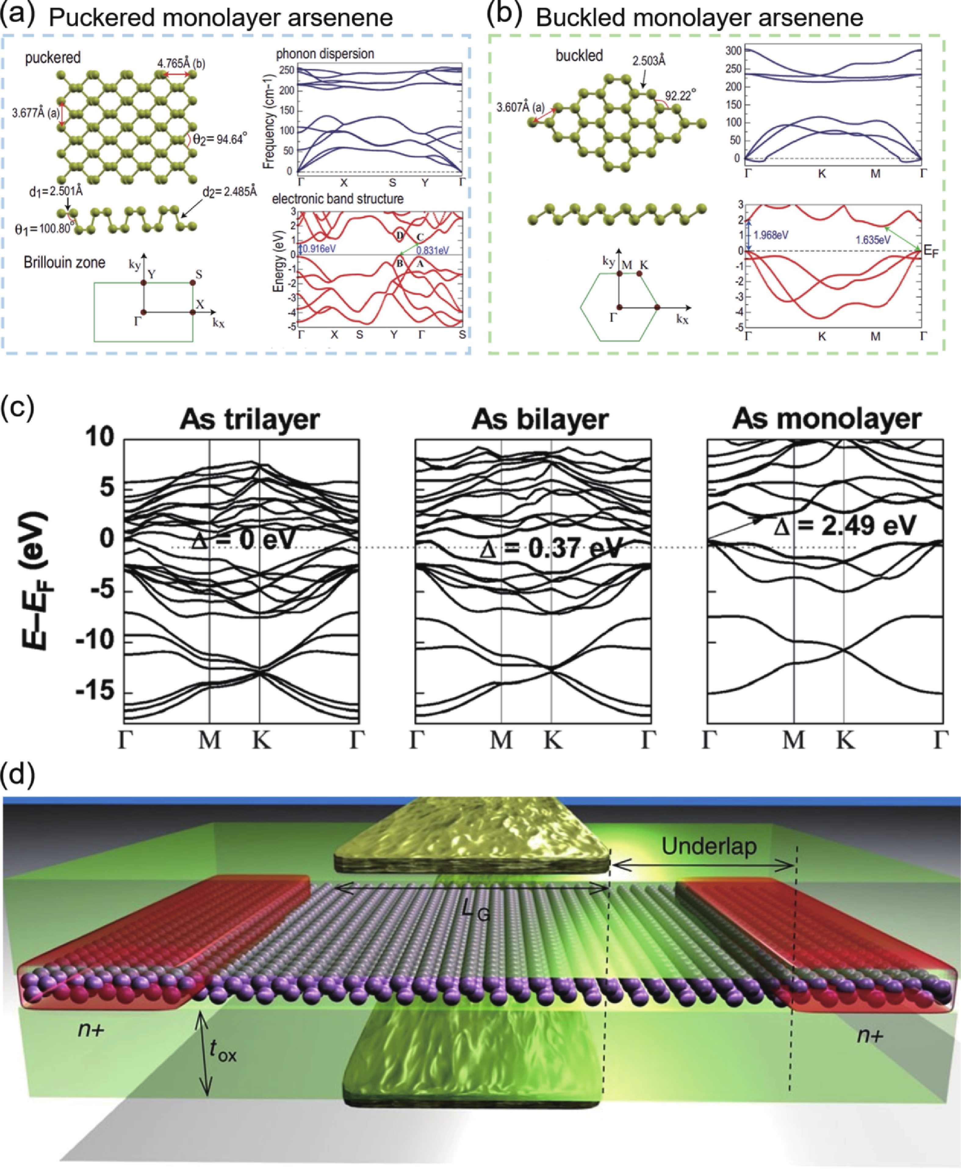
Kamal C, Ezawa M. Arsenene: two-dimensional buckled and puckered honeycomb arsenic systems. Phys Rev B, 2015, 91, 085423 doi: 10.1103/PhysRevB.91.085423 |
| [7] |
Zhang S, Yan Z, Li Y, et al. Atomically thin arsenene and antimonene: semimetal-semiconductor and indirect-direct band-gap transitions. Angew Chem Int Ed, 2015, 54, 3112 doi: 10.1002/anie.201411246 |
| [8] |
Zhang S, Xie M, Li F, et al. Semiconducting group 15 monolayers: a broad range of band gaps and high carrier mobilities. Angew Chem Int Ed, 2016, 55, 1666 doi: 10.1002/anie.201507568 |
| [9] |
Pizzi G, Gibertini M, Dib E, et al. Performance of arsenene and antimonene double-gate MOSFETs from first principles. Nat Commun, 2016, 7, 1 doi: 10.1038/ncomms12585 |
| [10] |
Wang Y, Ye M, Weng M, et al. Electrical contacts in monolayer arsenene devices. ACS Appl Mater Interfaces, 2017, 9, 29273 doi: 10.1021/acsami.7b08513 |
| [11] |
Wang Y, Huang P, Ye M, et al. Many-body effect, carrier mobility, and device performance of hexagonal arsenene and antimonene. Chem Mater, 2017, 29, 2191 doi: 10.1021/acs.chemmater.6b04909 |
| [12] |
Tsai H S, Wang S W, Hsiao C H, et al. Direct synthesis and practical bandgap estimation of multilayer arsenene nanoribbons. Chem Mater, 2016, 28, 425 doi: 10.1021/acs.chemmater.5b04949 |
| [13] |
Chen Y, Chen C, Kealhofer R, et al. Black arsenic: a layered semiconductor with extreme in-plane anisotropy. Adv Mater, 2018, 30, 1800754 doi: 10.1002/adma.201800754 |
| [14] |
Zhong M, Xia Q, Pan L, et al. Thickness-dependent carrier transport characteristics of a new 2D elemental semiconductor: black arsenic. Adv Funct Mater, 2018, 28, 1802581 doi: 10.1002/adfm.201802581 |
| [15] |
Qi Z H, Hu Y, Jin Z, et al. Tuning the liquid-phase exfoliation of arsenic nanosheets by interaction with various solvents. Phys Chem Chem Phys, 2019, 21, 12087 doi: 10.1039/C9CP01052A |
| [16] |
Wang X, Hu Y, Mo J, et al. Arsenene: a potential therapeutic agent for acute promyelocytic leukaemia cells by acting on nuclear proteins. Angew Chem Int Ed, 2020, 59, 5151 doi: 10.1002/anie.201913675 |
| [17] |
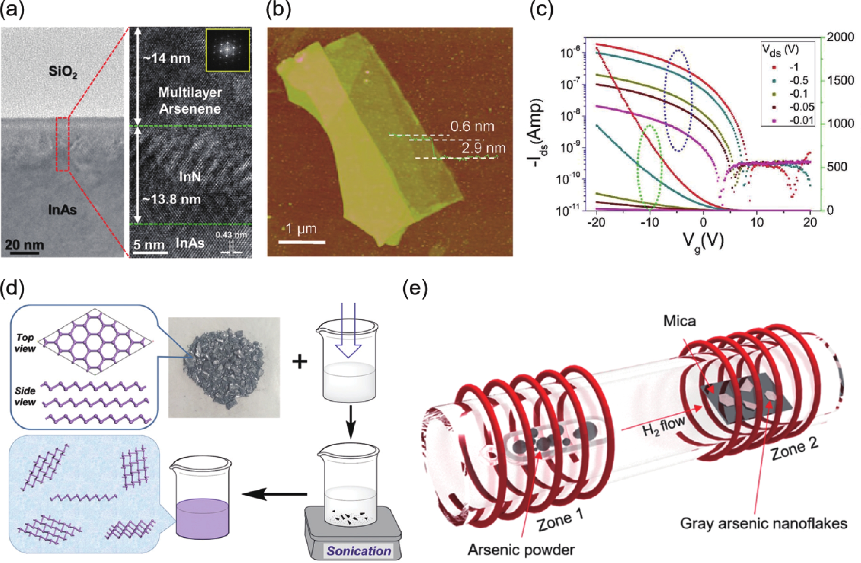
Hu Y, Qi Z H, Lu J, et al. Van der Waals epitaxial growth and interfacial passivation of two-dimensional single-crystalline few-layer gray arsenic nanoflakes. Chem Mater, 2019, 31, 4524 doi: 10.1021/acs.chemmater.9b01151 |
| [18] |
Hu Y, Wang X, Qi Z, et al. Wet chemistry vitrification and metal-to-semiconductor transition of 2D gray arsenene nanoflakes. Adv Funct Mater, 2021, 31, 2106529 doi: 10.1002/adfm.202106529 |


 DownLoad: