


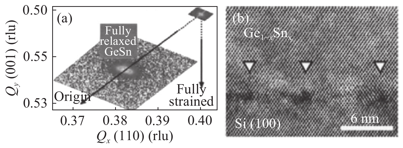
Fig. 1.
(a) Reciprocal space maps of the (224) reflections of Si substrate and GeSn layer indicating a strain-free film. (b) XTEM images of Ge1–xSnx/Si(100) (arrows indicate the Lomer defects). Data from Ref. [22].
SPECIAL ISSUE ON Si-BASED MATERIALS AND DEVICES
Jun Zheng1, 2, , Zhi Liu1, 2, Chunlai Xue1, 2, Chuanbo Li1, 2, Yuhua Zuo1, 2, Buwen Cheng1, 2 and Qiming Wang1, 2
Corresponding author: Jun Zheng, zhengjun@semi.ac.cn
Abstract: The GeSn binary alloy is a new group IV material that exhibits a direct bandgap when the Sn content exceeds 6%. It shows great potential for laser use in optoelectronic integration circuits (OEIC) on account of its low light emission efficiency arising from the indirect bandgap characteristics of Si and Ge. The bandgap of GeSn can be tuned from 0.6 to 0 eV by varying the Sn content, thus making this alloy suitable for use in near-infrared and mid-infrared detectors. In this paper, the growth of the GeSn alloy is first reviewed. Subsequently, GeSn photodetectors, light emitting diodes, and lasers are discussed. The GeSn alloy presents a promising pathway for the monolithic integration of Si photonic circuits by the complementary metal–oxide–semiconductor (CMOS) technology.
Key words: GeSn, material growth, Si photonics, optoelectronic integration
| [1] |
Heck M J R, Bowers J E. Energy efficient and energy proportional optical interconnects for multi-core processors: driving the need for on-chip sources. IEEE J Sel Top Quantum Electron, 2014, 20(4): 8201012 doi: 10.1109/JSTQE.2013.2293271
|
| [2] |
Soref R. Mid-infrared photonics in silicon and germanium. Nat Photon, 2010, 4: 495
|
| [3] |
Sun X C, Liu J F, Kimerling L C, et al. Direct gap photoluminescence of n-type tensile-strained Ge-on-Si. Appl Phys Lett, 2009, 95(1): 011911 doi: 10.1063/1.3170870
|
| [4] |
Chen Y H, Li C, Zhou Z W, et al. Room temperature photoluminescence of tensile-strained Ge/Si0.13Ge0.87 quantum wells grown on silicon-based germanium virtual substrate. Appl Phys Lett, 2009, 94(14): 141902 doi: 10.1063/1.3114408
|
| [5] |
Chaisakul P, Marris-Morini D, Isella G, et al. Room temperature direct gap electroluminescence from Ge/Si0.15Ge0.85 multiple quantum well waveguide. Appl Phys Lett, 2011, 99(14): 141106 doi: 10.1063/1.3647572
|
| [6] |
Wu P H, Dumcenco D, Huang Y S, et al. Above-room-temperature photoluminescence from a strain-compensated Ge/Si0.15Ge0.85 multiple-quantum-well structure. Appl Phys Lett, 2012, 100(14): 141905 doi: 10.1063/1.3700804
|
| [7] |
Liu Z, Hu W, Li C, et al. Room temperature direct-bandgap electroluminescence from n-type strain-compensated Ge/SiGe multiple quantum wells. Appl Phys Lett, 2012, 101(23): 231108 doi: 10.1063/1.4769834
|
| [8] |
Gallacher K, Velha P, Paul D J, et al. 1.55 μm direct bandgap electroluminescence from strained n-Ge quantum wells grown on Si substrates. Appl Phys Lett, 2012, 101(21): 211101 doi: 10.1063/1.4767138
|
| [9] |
Liu J F, Sun X C, Kimerling L C, et al. Direct-gap optical gain of Ge on Si at room temperature. Opt Lett, 2009, 34(11): 1738 doi: 10.1364/OL.34.001738
|
| [10] |
Süess M J, Carroll L, Sigg H, et al. Tensile strained Ge quantum wells on Si substrate: Post-growth annealing versus low temperature re-growth. Mater Sci Eng B, 2012, 177(10): 696 doi: 10.1016/j.mseb.2011.10.009
|
| [11] |
Sun X C, Liu J F, Kimerling L C, et al. Room-temperature direct bandgap electroluminesence from Ge-on-Si light-emitting diodes. Opt Lett, 2009, 34(8): 1198 doi: 10.1364/OL.34.001198
|
| [12] |
Hu W, Cheng B, Xue C, et al. Electroluminescence from Ge on Si substrate at room temperature. Appl Phys Lett, 2009, 95(9): 092102 doi: 10.1063/1.3216577
|
| [13] |
Cheng S L, Lu J, Shambat G, et al. Room temperature 1.6 microm electroluminescence from Ge light emitting diode on Si substrate. Opt Express, 2009, 17(12): 10019 doi: 10.1364/OE.17.010019
|
| [14] |
Chen R, Lin H, Huo Y, et al. Increased photoluminescence of strain-reduced, high-Sn composition Ge1-xSnx alloys grown by molecular beam epitaxy. Appl Phys Lett, 2011, 99(18): 181125 doi: 10.1063/1.3658632
|
| [15] |
Ghetmiri S A, Du W, Margetis J, et al. Direct-bandgap GeSn grown on silicon with 2230 nm photoluminescence. Appl Phys Lett, 2014, 105: 151109 doi: 10.1063/1.4898597
|
| [16] |
Low K L, Yang Y, Han G, et al. Electronic band structure and effective mass parameters of Ge1-xSnx alloys. J Appl Phys, 2012, 112: 103715 doi: 10.1063/1.4767381
|
| [17] |
Gupta S, Magyari-Köpe B, Nishi Y, et al. Achieving direct band gap in germanium through integration of Sn alloying and external strain. J Appl Phys, 2013, 113: 073707 doi: 10.1063/1.4792649
|
| [18] |
He G, Atwater H A. Interband transitions in SnxGe1-x alloys. Phys Rev Lett, 1997, 79: 1937 doi: 10.1103/PhysRevLett.79.1937
|
| [19] |
Taraci J, Tolle J, Kouvetakis J, et al. Simple chemical routes to diamond-cubic germanium-tin alloys. Appl Phys Lett, 2001, 78(23): 3607 doi: 10.1063/1.1376156
|
| [20] |
Taraci J, Zollner S, McCartney M R, et al. Synthesis of silicon-based infrared semiconductors in the Ge–Sn system using molecular chemistry methods. J Am Chem Soc, 2001, 123(44): 10980 doi: 10.1021/ja0115058
|
| [21] |
Bauer M, Taraci J, Tolle J, et al. Ge–Sn semiconductors for band-gap and lattice engineering. Appl Phys Lett, 2002, 81(6): 2992
|
| [22] |
Roucka R, Tolle J, Cook C, et al. Versatile buffer layer architectures based on Ge1-xSnx alloys. Appl Phys Lett, 2005, 86: 191912 doi: 10.1063/1.1922078
|
| [23] |
Vincent B, Gencarelli F, Bender H, et al. Undoped and in-situ B doped GeSn epitaxial growth on Ge by atmospheric pressure-chemical vapor deposition. Appl Phys Lett, 2011, 99: 152103 doi: 10.1063/1.3645620
|
| [24] |
Gencarelli F, Vincent B, Souriau L, et al. Low-temperature Ge and GeSn chemical vapor deposition using Ge2H6. Thin Solid Films, 2012, 520(8): 3211 doi: 10.1016/j.tsf.2011.10.119
|
| [25] |
Margetis J, Ghetmiri S A, Du W, et al. Growth and characterization of epitaxial Ge1-xSnx alloys and heterostructures using a commercial CVD system GeSn. Session 1: GeSn epitaxy, ECS Trans, 2014, 64: 711
|
| [26] |
Chen R, Huang Y C, Gupta S, et al. Material characterization of high Sn-content, compressively-strained GeSn epitaxial films after rapid thermal processing. J Cryst Growth, 2013, 365: 29 doi: 10.1016/j.jcrysgro.2012.12.014
|
| [27] |
Chen R, Huang Y C, Gupta S, et al. Flattening of low temperature epitaxial Ge1-xSnx/Ge/Si(100) alloys via mass transport during post-growth annealing. Appl Surf Sci, 2011, 257: 4468 doi: 10.1016/j.apsusc.2010.12.094
|
| [28] |
Su S, Wang W, Cheng B, et al. Epitaxial growth and thermal stability of Ge1-xSnx alloys on Ge-buffered Si(001) substrates. J Cryst Growth, 2011, 317: 43 doi: 10.1016/j.jcrysgro.2011.01.015
|
| [29] |
Oehme M, Buca D, Kostecki K, et al. Epitaxial growth of highly compressively strained GeSn alloys up to 12.5% Sn. J Cryst Growth, 2013, 384: 71 doi: 10.1016/j.jcrysgro.2013.09.018
|
| [30] |
Lieten R R, Seo J W, Decoster S, et al. Tensile strained GeSn on Si by solid phase epitaxy. Appl Phys Lett, 2013, 102: 052106 doi: 10.1063/1.4790302
|
| [31] |
Lieten R R, Seo J W, Decoster S, et al. Navarro-Contreras H, et al. Ge1-xSnxGe1-xSnx alloys pseudomorphically grown on Ge (001). Appl Phys Lett, 2003, 83: 4942 doi: 10.1063/1.1634374
|
| [32] |
Zheng J,Li L L,Zhou T W,et al. Growth of crystalline Ge1-xSnx films on Si (100) by magnetron sputtering. ECS Solid State Lett, 2014, 3(9): 111 doi: 10.1149/2.0081409ssl
|
| [33] |
Tsukamoto T, Hirose N, Kasamatsu A, et al. Formation of GeSn layers on Si (001) substrates at high growth temperature and high deposition rate by sputter epitaxy method. J Mater Sci, 2015, 50: 4366 doi: 10.1007/s10853-015-8990-4
|
| [34] |
Li H F, Brouillet J, Alan A, et al. Low temperature growth of high crystallinity GeSn on amorphous layers for advanced optoelectronics. Opt Mater Express, 2013, 3: 1385 doi: 10.1364/OME.3.001385
|
| [35] |
Su S J, Cheng B W, Xue C L, et al. GeSn p–i–n photodetector for all telecommunication bands detection. Opt Express, 2011, 19(7): 6400 doi: 10.1364/OE.19.006400
|
| [36] |
Zhang D, Xue C, Cheng B, et al. High-responsivity GeSn short-wave infrared p–i–n photodetectors. Appl Phys Lett, 2013, 102(14): 141111 doi: 10.1063/1.4801957
|
| [37] |
Tseng H H, Li H, Mashanov V, et al. GeSn-based p-i-n photodiodes with strained active layer on a Si wafer. Appl Phys Lett, 2013, 103: 231907 doi: 10.1063/1.4840135
|
| [38] |
Dong Y, Wang W, Lei D, et al. Suppression of dark current in germanium-tin on silicon p–i–n photodiode by a silicon surface passivation technique. Opt Express, 2015, 23(14): 18611 doi: 10.1364/OE.23.018611
|
| [39] |
Oehme M, Widmann D, Kostecki K, et al. GeSn/Ge multiquantum well photodetectors on Si substrates. Opt Lett, 2014, 39(16): 4711 doi: 10.1364/OL.39.004711
|
| [40] |
Zheng J, Wang S Y, Liu Z, et al. GeSn p–i–n photodetectors with GeSn layer grown by magnetron sputtering epitaxy. Appl Phys Lett, 2016, 108(3): 033503 doi: 10.1063/1.4940194
|
| [41] |
Chang C, Li H, Huang H, et al. Sn-based Ge/Ge0.975Sn0.025/Ge p–i–n photodetector operated with back-side illumination. Appl Phys Lett, 2016, 108: 151101 doi: 10.1063/1.4945816
|
| [42] |
Conley B R, Margetis J, Du W, et al. Si based GeSn photoconductors with a 1.63 A/W peak responsivity and a 2.4 μm long wavelength cutoff. Appl Phys Lett, 2014, 105: 221117 doi: 10.1063/1.4903540
|
| [43] |
Conley B R, Mosleh A, Ghetmiri S A, et al. Temperature dependent spectral response and detectivity of GeSn photoconductors on silicon for short wave infrared detection. Opt Express, 2014, 22(13): 15639 doi: 10.1364/OE.22.015639
|
| [44] |
Oehme M, Kostecki K, Arguirov T, et al. GeSn heterojunction LEDs on Si substrates. IEEE Photonics Technol Lett, 2014, 26(2): 187 doi: 10.1109/LPT.2013.2291571
|
| [45] |
Gupta J P, Bhargava N, Kim S, et al. Infrared electroluminescence from GeSn heterojunction diodes grown by molecular beam epitaxy. Appl Phys Lett, 2013, 102: 251117 doi: 10.1063/1.4812747
|
| [46] |
Tseng H H, Wu K Y, Li H, et al. Mid-infrared electroluminescence from a Ge/Ge0.922Sn0.078/Ge double heterostructure p–i–n diode on a Si substrate. Appl Phys Lett, 2013, 102(18): 182106 doi: 10.1063/1.4804675
|
| [47] |
Stange D, von den Driesch N, Rainko D, et al. Study of GeSn based heterostructures: towards optimized group IV MQW LEDs. Opt Express, 2016, 24(2): 1358 doi: 10.1364/OE.24.001358
|
| [48] |
Wirths S, Geiger R, von den Driesch N, et al. Lasing in direct-bandgap GeSn alloy grown on Si. Nat Photonics, 2015, 9: 88 doi: 10.1038/nphoton.2014.321
|
| [49] |
Al-Kabi S, Ghetmiri S A, Margetis J, et al. An optically pumped 2.5 μm GeSn laser on Si operating at 110 K. Appl Phys Lett, 2016, 109: 171105 doi: 10.1063/1.4966141
|
| [50] |
Stange D, Wirths S, Geiger R, et al. Optically pumped GeSn microdisk lasers on Si. ACS Photonics, 2016, 3: 1279 doi: 10.1021/acsphotonics.6b00258
|


Table 1. Summary of GeSn PIN detectors reported in literature.
| Parameter | Ref. [35] | Ref. [36] | Ref. [37] | Ref. [38] | Ref. [39] | Ref. [40] |
| Sn content | 3% | 3.65% | 3.85% | 5% | 6.9% | 6% |
| GeSn thickness (nm) | 820 | 750 | 300 | 360 | 120 | 500 |
| J dark @ −1 V (A/cm2) | 1.8 | 0.006 | 0.4 | 0.073 | 0.8 | 0.22 |
| R @ 1600 nm (A/W) | 0.15 @ −1 V | 0.25 @ 0 V | 0.2 @ 0 V | 0.1 −1 V | 0.13 @ 0 V | 0.22 @ 0 V |
| Cut-off wavelength (nm) | 1800 | 2100 | 1800 | 1900 | 2000 | 1985 |
| GeSn growth by | MBE | MBE | MBE | MBE | MBE | Sputter |
 DownLoad: CSV
| [1] |
Heck M J R, Bowers J E. Energy efficient and energy proportional optical interconnects for multi-core processors: driving the need for on-chip sources. IEEE J Sel Top Quantum Electron, 2014, 20(4): 8201012 doi: 10.1109/JSTQE.2013.2293271
|
| [2] |
Soref R. Mid-infrared photonics in silicon and germanium. Nat Photon, 2010, 4: 495
|
| [3] |
Sun X C, Liu J F, Kimerling L C, et al. Direct gap photoluminescence of n-type tensile-strained Ge-on-Si. Appl Phys Lett, 2009, 95(1): 011911 doi: 10.1063/1.3170870
|
| [4] |
Chen Y H, Li C, Zhou Z W, et al. Room temperature photoluminescence of tensile-strained Ge/Si0.13Ge0.87 quantum wells grown on silicon-based germanium virtual substrate. Appl Phys Lett, 2009, 94(14): 141902 doi: 10.1063/1.3114408
|
| [5] |
Chaisakul P, Marris-Morini D, Isella G, et al. Room temperature direct gap electroluminescence from Ge/Si0.15Ge0.85 multiple quantum well waveguide. Appl Phys Lett, 2011, 99(14): 141106 doi: 10.1063/1.3647572
|
| [6] |
Wu P H, Dumcenco D, Huang Y S, et al. Above-room-temperature photoluminescence from a strain-compensated Ge/Si0.15Ge0.85 multiple-quantum-well structure. Appl Phys Lett, 2012, 100(14): 141905 doi: 10.1063/1.3700804
|
| [7] |
Liu Z, Hu W, Li C, et al. Room temperature direct-bandgap electroluminescence from n-type strain-compensated Ge/SiGe multiple quantum wells. Appl Phys Lett, 2012, 101(23): 231108 doi: 10.1063/1.4769834
|
| [8] |
Gallacher K, Velha P, Paul D J, et al. 1.55 μm direct bandgap electroluminescence from strained n-Ge quantum wells grown on Si substrates. Appl Phys Lett, 2012, 101(21): 211101 doi: 10.1063/1.4767138
|
| [9] |
Liu J F, Sun X C, Kimerling L C, et al. Direct-gap optical gain of Ge on Si at room temperature. Opt Lett, 2009, 34(11): 1738 doi: 10.1364/OL.34.001738
|
| [10] |
Süess M J, Carroll L, Sigg H, et al. Tensile strained Ge quantum wells on Si substrate: Post-growth annealing versus low temperature re-growth. Mater Sci Eng B, 2012, 177(10): 696 doi: 10.1016/j.mseb.2011.10.009
|
| [11] |
Sun X C, Liu J F, Kimerling L C, et al. Room-temperature direct bandgap electroluminesence from Ge-on-Si light-emitting diodes. Opt Lett, 2009, 34(8): 1198 doi: 10.1364/OL.34.001198
|
| [12] |
Hu W, Cheng B, Xue C, et al. Electroluminescence from Ge on Si substrate at room temperature. Appl Phys Lett, 2009, 95(9): 092102 doi: 10.1063/1.3216577
|
| [13] |
Cheng S L, Lu J, Shambat G, et al. Room temperature 1.6 microm electroluminescence from Ge light emitting diode on Si substrate. Opt Express, 2009, 17(12): 10019 doi: 10.1364/OE.17.010019
|
| [14] |
Chen R, Lin H, Huo Y, et al. Increased photoluminescence of strain-reduced, high-Sn composition Ge1-xSnx alloys grown by molecular beam epitaxy. Appl Phys Lett, 2011, 99(18): 181125 doi: 10.1063/1.3658632
|
| [15] |
Ghetmiri S A, Du W, Margetis J, et al. Direct-bandgap GeSn grown on silicon with 2230 nm photoluminescence. Appl Phys Lett, 2014, 105: 151109 doi: 10.1063/1.4898597
|
| [16] |
Low K L, Yang Y, Han G, et al. Electronic band structure and effective mass parameters of Ge1-xSnx alloys. J Appl Phys, 2012, 112: 103715 doi: 10.1063/1.4767381
|
| [17] |
Gupta S, Magyari-Köpe B, Nishi Y, et al. Achieving direct band gap in germanium through integration of Sn alloying and external strain. J Appl Phys, 2013, 113: 073707 doi: 10.1063/1.4792649
|
| [18] |
He G, Atwater H A. Interband transitions in SnxGe1-x alloys. Phys Rev Lett, 1997, 79: 1937 doi: 10.1103/PhysRevLett.79.1937
|
| [19] |
Taraci J, Tolle J, Kouvetakis J, et al. Simple chemical routes to diamond-cubic germanium-tin alloys. Appl Phys Lett, 2001, 78(23): 3607 doi: 10.1063/1.1376156
|
| [20] |
Taraci J, Zollner S, McCartney M R, et al. Synthesis of silicon-based infrared semiconductors in the Ge–Sn system using molecular chemistry methods. J Am Chem Soc, 2001, 123(44): 10980 doi: 10.1021/ja0115058
|
| [21] |
Bauer M, Taraci J, Tolle J, et al. Ge–Sn semiconductors for band-gap and lattice engineering. Appl Phys Lett, 2002, 81(6): 2992
|
| [22] |
Roucka R, Tolle J, Cook C, et al. Versatile buffer layer architectures based on Ge1-xSnx alloys. Appl Phys Lett, 2005, 86: 191912 doi: 10.1063/1.1922078
|
| [23] |
Vincent B, Gencarelli F, Bender H, et al. Undoped and in-situ B doped GeSn epitaxial growth on Ge by atmospheric pressure-chemical vapor deposition. Appl Phys Lett, 2011, 99: 152103 doi: 10.1063/1.3645620
|
| [24] |
Gencarelli F, Vincent B, Souriau L, et al. Low-temperature Ge and GeSn chemical vapor deposition using Ge2H6. Thin Solid Films, 2012, 520(8): 3211 doi: 10.1016/j.tsf.2011.10.119
|
| [25] |
Margetis J, Ghetmiri S A, Du W, et al. Growth and characterization of epitaxial Ge1-xSnx alloys and heterostructures using a commercial CVD system GeSn. Session 1: GeSn epitaxy, ECS Trans, 2014, 64: 711
|
| [26] |
Chen R, Huang Y C, Gupta S, et al. Material characterization of high Sn-content, compressively-strained GeSn epitaxial films after rapid thermal processing. J Cryst Growth, 2013, 365: 29 doi: 10.1016/j.jcrysgro.2012.12.014
|
| [27] |
Chen R, Huang Y C, Gupta S, et al. Flattening of low temperature epitaxial Ge1-xSnx/Ge/Si(100) alloys via mass transport during post-growth annealing. Appl Surf Sci, 2011, 257: 4468 doi: 10.1016/j.apsusc.2010.12.094
|
| [28] |
Su S, Wang W, Cheng B, et al. Epitaxial growth and thermal stability of Ge1-xSnx alloys on Ge-buffered Si(001) substrates. J Cryst Growth, 2011, 317: 43 doi: 10.1016/j.jcrysgro.2011.01.015
|
| [29] |
Oehme M, Buca D, Kostecki K, et al. Epitaxial growth of highly compressively strained GeSn alloys up to 12.5% Sn. J Cryst Growth, 2013, 384: 71 doi: 10.1016/j.jcrysgro.2013.09.018
|
| [30] |
Lieten R R, Seo J W, Decoster S, et al. Tensile strained GeSn on Si by solid phase epitaxy. Appl Phys Lett, 2013, 102: 052106 doi: 10.1063/1.4790302
|
| [31] |
Lieten R R, Seo J W, Decoster S, et al. Navarro-Contreras H, et al. Ge1-xSnxGe1-xSnx alloys pseudomorphically grown on Ge (001). Appl Phys Lett, 2003, 83: 4942 doi: 10.1063/1.1634374
|
| [32] |
Zheng J,Li L L,Zhou T W,et al. Growth of crystalline Ge1-xSnx films on Si (100) by magnetron sputtering. ECS Solid State Lett, 2014, 3(9): 111 doi: 10.1149/2.0081409ssl
|
| [33] |
Tsukamoto T, Hirose N, Kasamatsu A, et al. Formation of GeSn layers on Si (001) substrates at high growth temperature and high deposition rate by sputter epitaxy method. J Mater Sci, 2015, 50: 4366 doi: 10.1007/s10853-015-8990-4
|
| [34] |
Li H F, Brouillet J, Alan A, et al. Low temperature growth of high crystallinity GeSn on amorphous layers for advanced optoelectronics. Opt Mater Express, 2013, 3: 1385 doi: 10.1364/OME.3.001385
|
| [35] |
Su S J, Cheng B W, Xue C L, et al. GeSn p–i–n photodetector for all telecommunication bands detection. Opt Express, 2011, 19(7): 6400 doi: 10.1364/OE.19.006400
|
| [36] |
Zhang D, Xue C, Cheng B, et al. High-responsivity GeSn short-wave infrared p–i–n photodetectors. Appl Phys Lett, 2013, 102(14): 141111 doi: 10.1063/1.4801957
|
| [37] |
Tseng H H, Li H, Mashanov V, et al. GeSn-based p-i-n photodiodes with strained active layer on a Si wafer. Appl Phys Lett, 2013, 103: 231907 doi: 10.1063/1.4840135
|
| [38] |
Dong Y, Wang W, Lei D, et al. Suppression of dark current in germanium-tin on silicon p–i–n photodiode by a silicon surface passivation technique. Opt Express, 2015, 23(14): 18611 doi: 10.1364/OE.23.018611
|
| [39] |
Oehme M, Widmann D, Kostecki K, et al. GeSn/Ge multiquantum well photodetectors on Si substrates. Opt Lett, 2014, 39(16): 4711 doi: 10.1364/OL.39.004711
|
| [40] |
Zheng J, Wang S Y, Liu Z, et al. GeSn p–i–n photodetectors with GeSn layer grown by magnetron sputtering epitaxy. Appl Phys Lett, 2016, 108(3): 033503 doi: 10.1063/1.4940194
|
| [41] |
Chang C, Li H, Huang H, et al. Sn-based Ge/Ge0.975Sn0.025/Ge p–i–n photodetector operated with back-side illumination. Appl Phys Lett, 2016, 108: 151101 doi: 10.1063/1.4945816
|
| [42] |
Conley B R, Margetis J, Du W, et al. Si based GeSn photoconductors with a 1.63 A/W peak responsivity and a 2.4 μm long wavelength cutoff. Appl Phys Lett, 2014, 105: 221117 doi: 10.1063/1.4903540
|
| [43] |
Conley B R, Mosleh A, Ghetmiri S A, et al. Temperature dependent spectral response and detectivity of GeSn photoconductors on silicon for short wave infrared detection. Opt Express, 2014, 22(13): 15639 doi: 10.1364/OE.22.015639
|
| [44] |
Oehme M, Kostecki K, Arguirov T, et al. GeSn heterojunction LEDs on Si substrates. IEEE Photonics Technol Lett, 2014, 26(2): 187 doi: 10.1109/LPT.2013.2291571
|
| [45] |
Gupta J P, Bhargava N, Kim S, et al. Infrared electroluminescence from GeSn heterojunction diodes grown by molecular beam epitaxy. Appl Phys Lett, 2013, 102: 251117 doi: 10.1063/1.4812747
|
| [46] |
Tseng H H, Wu K Y, Li H, et al. Mid-infrared electroluminescence from a Ge/Ge0.922Sn0.078/Ge double heterostructure p–i–n diode on a Si substrate. Appl Phys Lett, 2013, 102(18): 182106 doi: 10.1063/1.4804675
|
| [47] |
Stange D, von den Driesch N, Rainko D, et al. Study of GeSn based heterostructures: towards optimized group IV MQW LEDs. Opt Express, 2016, 24(2): 1358 doi: 10.1364/OE.24.001358
|
| [48] |
Wirths S, Geiger R, von den Driesch N, et al. Lasing in direct-bandgap GeSn alloy grown on Si. Nat Photonics, 2015, 9: 88 doi: 10.1038/nphoton.2014.321
|
| [49] |
Al-Kabi S, Ghetmiri S A, Margetis J, et al. An optically pumped 2.5 μm GeSn laser on Si operating at 110 K. Appl Phys Lett, 2016, 109: 171105 doi: 10.1063/1.4966141
|
| [50] |
Stange D, Wirths S, Geiger R, et al. Optically pumped GeSn microdisk lasers on Si. ACS Photonics, 2016, 3: 1279 doi: 10.1021/acsphotonics.6b00258
|


Article views: 5301 Times PDF downloads: 198 Times Cited by: 0 Times
Received: 03 November 2017 Revised: 30 January 2018 Online: Published: 01 June 2018
| Citation: |
Jun Zheng, Zhi Liu, Chunlai Xue, Chuanbo Li, Yuhua Zuo, Buwen Cheng, Qiming Wang. Recent progress in GeSn growth and GeSn-based photonic devices[J]. Journal of Semiconductors, 2018, 39(6): 061006. doi: 10.1088/1674-4926/39/6/061006
J Zheng, Z Liu, C L Xue, C B Li, Y H Zuo, B W Cheng, Q M Wang. Recent progress in GeSn growth and GeSn-based photonic devices[J]. J. Semicond., 2018, 39(6): 061006. doi: 10.1088/1674-4926/39/6/061006.
Export: BibTex EndNote

|
| [1] |
Heck M J R, Bowers J E. Energy efficient and energy proportional optical interconnects for multi-core processors: driving the need for on-chip sources. IEEE J Sel Top Quantum Electron, 2014, 20(4): 8201012 doi: 10.1109/JSTQE.2013.2293271
|
| [2] |
Soref R. Mid-infrared photonics in silicon and germanium. Nat Photon, 2010, 4: 495
|
| [3] |
Sun X C, Liu J F, Kimerling L C, et al. Direct gap photoluminescence of n-type tensile-strained Ge-on-Si. Appl Phys Lett, 2009, 95(1): 011911 doi: 10.1063/1.3170870
|
| [4] |
Chen Y H, Li C, Zhou Z W, et al. Room temperature photoluminescence of tensile-strained Ge/Si0.13Ge0.87 quantum wells grown on silicon-based germanium virtual substrate. Appl Phys Lett, 2009, 94(14): 141902 doi: 10.1063/1.3114408
|
| [5] |
Chaisakul P, Marris-Morini D, Isella G, et al. Room temperature direct gap electroluminescence from Ge/Si0.15Ge0.85 multiple quantum well waveguide. Appl Phys Lett, 2011, 99(14): 141106 doi: 10.1063/1.3647572
|
| [6] |
Wu P H, Dumcenco D, Huang Y S, et al. Above-room-temperature photoluminescence from a strain-compensated Ge/Si0.15Ge0.85 multiple-quantum-well structure. Appl Phys Lett, 2012, 100(14): 141905 doi: 10.1063/1.3700804
|
| [7] |
Liu Z, Hu W, Li C, et al. Room temperature direct-bandgap electroluminescence from n-type strain-compensated Ge/SiGe multiple quantum wells. Appl Phys Lett, 2012, 101(23): 231108 doi: 10.1063/1.4769834
|
| [8] |
Gallacher K, Velha P, Paul D J, et al. 1.55 μm direct bandgap electroluminescence from strained n-Ge quantum wells grown on Si substrates. Appl Phys Lett, 2012, 101(21): 211101 doi: 10.1063/1.4767138
|
| [9] |
Liu J F, Sun X C, Kimerling L C, et al. Direct-gap optical gain of Ge on Si at room temperature. Opt Lett, 2009, 34(11): 1738 doi: 10.1364/OL.34.001738
|
| [10] |
Süess M J, Carroll L, Sigg H, et al. Tensile strained Ge quantum wells on Si substrate: Post-growth annealing versus low temperature re-growth. Mater Sci Eng B, 2012, 177(10): 696 doi: 10.1016/j.mseb.2011.10.009
|
| [11] |
Sun X C, Liu J F, Kimerling L C, et al. Room-temperature direct bandgap electroluminesence from Ge-on-Si light-emitting diodes. Opt Lett, 2009, 34(8): 1198 doi: 10.1364/OL.34.001198
|
| [12] |
Hu W, Cheng B, Xue C, et al. Electroluminescence from Ge on Si substrate at room temperature. Appl Phys Lett, 2009, 95(9): 092102 doi: 10.1063/1.3216577
|
| [13] |
Cheng S L, Lu J, Shambat G, et al. Room temperature 1.6 microm electroluminescence from Ge light emitting diode on Si substrate. Opt Express, 2009, 17(12): 10019 doi: 10.1364/OE.17.010019
|
| [14] |
Chen R, Lin H, Huo Y, et al. Increased photoluminescence of strain-reduced, high-Sn composition Ge1-xSnx alloys grown by molecular beam epitaxy. Appl Phys Lett, 2011, 99(18): 181125 doi: 10.1063/1.3658632
|
| [15] |
Ghetmiri S A, Du W, Margetis J, et al. Direct-bandgap GeSn grown on silicon with 2230 nm photoluminescence. Appl Phys Lett, 2014, 105: 151109 doi: 10.1063/1.4898597
|
| [16] |
Low K L, Yang Y, Han G, et al. Electronic band structure and effective mass parameters of Ge1-xSnx alloys. J Appl Phys, 2012, 112: 103715 doi: 10.1063/1.4767381
|
| [17] |
Gupta S, Magyari-Köpe B, Nishi Y, et al. Achieving direct band gap in germanium through integration of Sn alloying and external strain. J Appl Phys, 2013, 113: 073707 doi: 10.1063/1.4792649
|
| [18] |
He G, Atwater H A. Interband transitions in SnxGe1-x alloys. Phys Rev Lett, 1997, 79: 1937 doi: 10.1103/PhysRevLett.79.1937
|
| [19] |
Taraci J, Tolle J, Kouvetakis J, et al. Simple chemical routes to diamond-cubic germanium-tin alloys. Appl Phys Lett, 2001, 78(23): 3607 doi: 10.1063/1.1376156
|
| [20] |
Taraci J, Zollner S, McCartney M R, et al. Synthesis of silicon-based infrared semiconductors in the Ge–Sn system using molecular chemistry methods. J Am Chem Soc, 2001, 123(44): 10980 doi: 10.1021/ja0115058
|
| [21] |
Bauer M, Taraci J, Tolle J, et al. Ge–Sn semiconductors for band-gap and lattice engineering. Appl Phys Lett, 2002, 81(6): 2992
|
| [22] |
Roucka R, Tolle J, Cook C, et al. Versatile buffer layer architectures based on Ge1-xSnx alloys. Appl Phys Lett, 2005, 86: 191912 doi: 10.1063/1.1922078
|
| [23] |
Vincent B, Gencarelli F, Bender H, et al. Undoped and in-situ B doped GeSn epitaxial growth on Ge by atmospheric pressure-chemical vapor deposition. Appl Phys Lett, 2011, 99: 152103 doi: 10.1063/1.3645620
|
| [24] |
Gencarelli F, Vincent B, Souriau L, et al. Low-temperature Ge and GeSn chemical vapor deposition using Ge2H6. Thin Solid Films, 2012, 520(8): 3211 doi: 10.1016/j.tsf.2011.10.119
|
| [25] |
Margetis J, Ghetmiri S A, Du W, et al. Growth and characterization of epitaxial Ge1-xSnx alloys and heterostructures using a commercial CVD system GeSn. Session 1: GeSn epitaxy, ECS Trans, 2014, 64: 711
|
| [26] |
Chen R, Huang Y C, Gupta S, et al. Material characterization of high Sn-content, compressively-strained GeSn epitaxial films after rapid thermal processing. J Cryst Growth, 2013, 365: 29 doi: 10.1016/j.jcrysgro.2012.12.014
|
| [27] |
Chen R, Huang Y C, Gupta S, et al. Flattening of low temperature epitaxial Ge1-xSnx/Ge/Si(100) alloys via mass transport during post-growth annealing. Appl Surf Sci, 2011, 257: 4468 doi: 10.1016/j.apsusc.2010.12.094
|
| [28] |
Su S, Wang W, Cheng B, et al. Epitaxial growth and thermal stability of Ge1-xSnx alloys on Ge-buffered Si(001) substrates. J Cryst Growth, 2011, 317: 43 doi: 10.1016/j.jcrysgro.2011.01.015
|
| [29] |
Oehme M, Buca D, Kostecki K, et al. Epitaxial growth of highly compressively strained GeSn alloys up to 12.5% Sn. J Cryst Growth, 2013, 384: 71 doi: 10.1016/j.jcrysgro.2013.09.018
|
| [30] |
Lieten R R, Seo J W, Decoster S, et al. Tensile strained GeSn on Si by solid phase epitaxy. Appl Phys Lett, 2013, 102: 052106 doi: 10.1063/1.4790302
|
| [31] |
Lieten R R, Seo J W, Decoster S, et al. Navarro-Contreras H, et al. Ge1-xSnxGe1-xSnx alloys pseudomorphically grown on Ge (001). Appl Phys Lett, 2003, 83: 4942 doi: 10.1063/1.1634374
|
| [32] |
Zheng J,Li L L,Zhou T W,et al. Growth of crystalline Ge1-xSnx films on Si (100) by magnetron sputtering. ECS Solid State Lett, 2014, 3(9): 111 doi: 10.1149/2.0081409ssl
|
| [33] |
Tsukamoto T, Hirose N, Kasamatsu A, et al. Formation of GeSn layers on Si (001) substrates at high growth temperature and high deposition rate by sputter epitaxy method. J Mater Sci, 2015, 50: 4366 doi: 10.1007/s10853-015-8990-4
|
| [34] |
Li H F, Brouillet J, Alan A, et al. Low temperature growth of high crystallinity GeSn on amorphous layers for advanced optoelectronics. Opt Mater Express, 2013, 3: 1385 doi: 10.1364/OME.3.001385
|
| [35] |
Su S J, Cheng B W, Xue C L, et al. GeSn p–i–n photodetector for all telecommunication bands detection. Opt Express, 2011, 19(7): 6400 doi: 10.1364/OE.19.006400
|
| [36] |
Zhang D, Xue C, Cheng B, et al. High-responsivity GeSn short-wave infrared p–i–n photodetectors. Appl Phys Lett, 2013, 102(14): 141111 doi: 10.1063/1.4801957
|
| [37] |
Tseng H H, Li H, Mashanov V, et al. GeSn-based p-i-n photodiodes with strained active layer on a Si wafer. Appl Phys Lett, 2013, 103: 231907 doi: 10.1063/1.4840135
|
| [38] |
Dong Y, Wang W, Lei D, et al. Suppression of dark current in germanium-tin on silicon p–i–n photodiode by a silicon surface passivation technique. Opt Express, 2015, 23(14): 18611 doi: 10.1364/OE.23.018611
|
| [39] |
Oehme M, Widmann D, Kostecki K, et al. GeSn/Ge multiquantum well photodetectors on Si substrates. Opt Lett, 2014, 39(16): 4711 doi: 10.1364/OL.39.004711
|
| [40] |
Zheng J, Wang S Y, Liu Z, et al. GeSn p–i–n photodetectors with GeSn layer grown by magnetron sputtering epitaxy. Appl Phys Lett, 2016, 108(3): 033503 doi: 10.1063/1.4940194
|
| [41] |
Chang C, Li H, Huang H, et al. Sn-based Ge/Ge0.975Sn0.025/Ge p–i–n photodetector operated with back-side illumination. Appl Phys Lett, 2016, 108: 151101 doi: 10.1063/1.4945816
|
| [42] |
Conley B R, Margetis J, Du W, et al. Si based GeSn photoconductors with a 1.63 A/W peak responsivity and a 2.4 μm long wavelength cutoff. Appl Phys Lett, 2014, 105: 221117 doi: 10.1063/1.4903540
|
| [43] |
Conley B R, Mosleh A, Ghetmiri S A, et al. Temperature dependent spectral response and detectivity of GeSn photoconductors on silicon for short wave infrared detection. Opt Express, 2014, 22(13): 15639 doi: 10.1364/OE.22.015639
|
| [44] |
Oehme M, Kostecki K, Arguirov T, et al. GeSn heterojunction LEDs on Si substrates. IEEE Photonics Technol Lett, 2014, 26(2): 187 doi: 10.1109/LPT.2013.2291571
|
| [45] |
Gupta J P, Bhargava N, Kim S, et al. Infrared electroluminescence from GeSn heterojunction diodes grown by molecular beam epitaxy. Appl Phys Lett, 2013, 102: 251117 doi: 10.1063/1.4812747
|
| [46] |
Tseng H H, Wu K Y, Li H, et al. Mid-infrared electroluminescence from a Ge/Ge0.922Sn0.078/Ge double heterostructure p–i–n diode on a Si substrate. Appl Phys Lett, 2013, 102(18): 182106 doi: 10.1063/1.4804675
|
| [47] |
Stange D, von den Driesch N, Rainko D, et al. Study of GeSn based heterostructures: towards optimized group IV MQW LEDs. Opt Express, 2016, 24(2): 1358 doi: 10.1364/OE.24.001358
|
| [48] |
Wirths S, Geiger R, von den Driesch N, et al. Lasing in direct-bandgap GeSn alloy grown on Si. Nat Photonics, 2015, 9: 88 doi: 10.1038/nphoton.2014.321
|
| [49] |
Al-Kabi S, Ghetmiri S A, Margetis J, et al. An optically pumped 2.5 μm GeSn laser on Si operating at 110 K. Appl Phys Lett, 2016, 109: 171105 doi: 10.1063/1.4966141
|
| [50] |
Stange D, Wirths S, Geiger R, et al. Optically pumped GeSn microdisk lasers on Si. ACS Photonics, 2016, 3: 1279 doi: 10.1021/acsphotonics.6b00258
|

 WeChat ID
Journal of Semiconductors © 2017 All Rights Reserved 京ICP备05085259号-2


