Fig. 1.
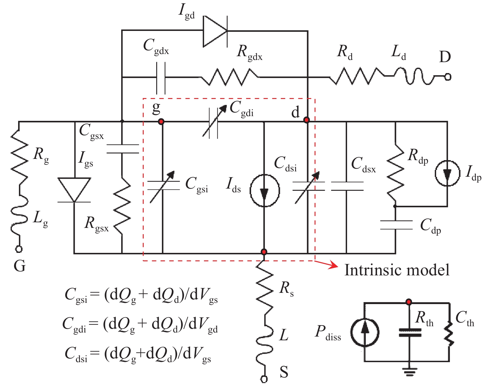
(Color online) Large-signal model topology for compound semiconductor HEMTs.
SEMICONDUCTOR DEVICES
Tianhao Li, Wenjun Li and Jun Liu
Corresponding author: Wenjun Li, Email: liwenjun@hdu.edu.cn
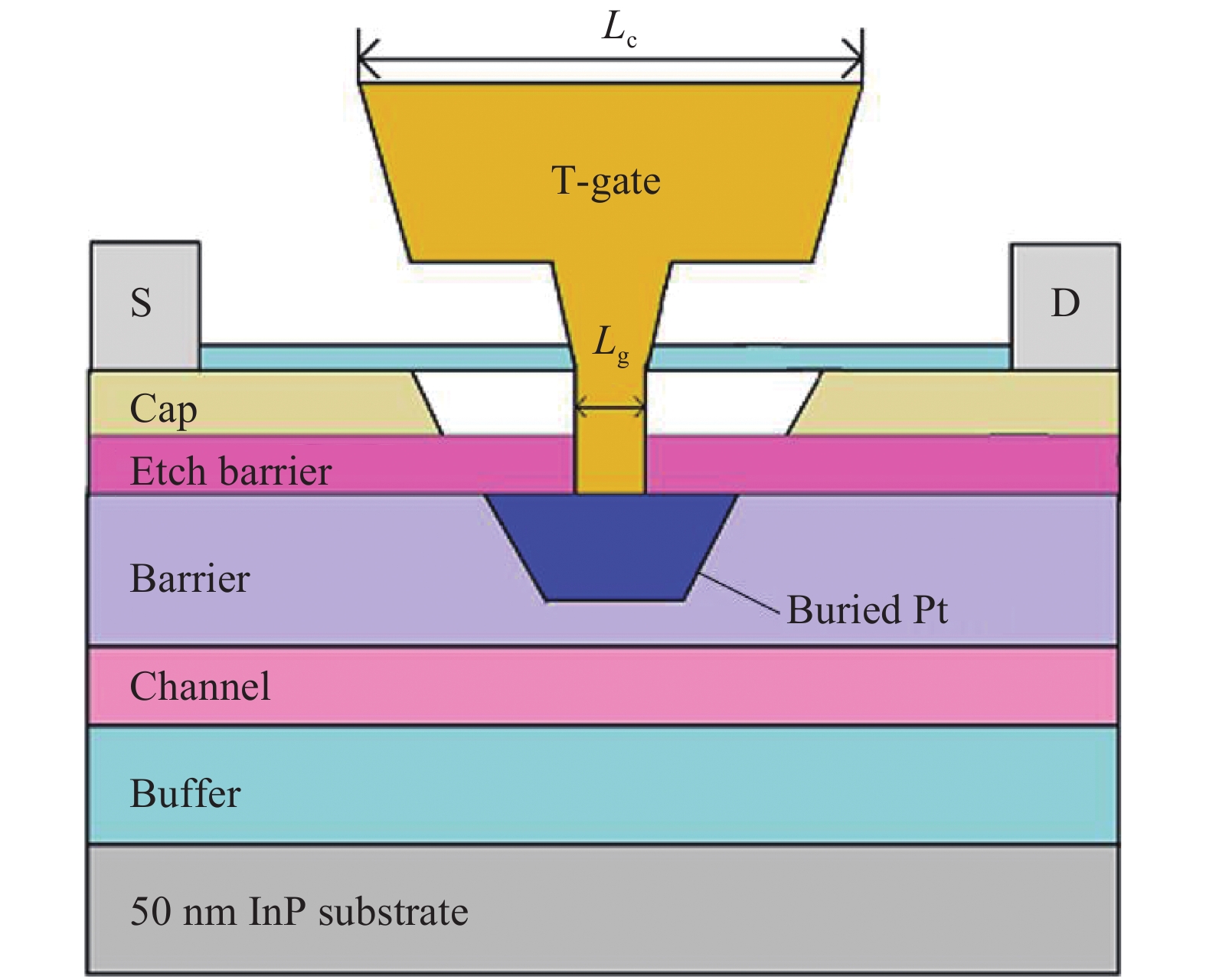
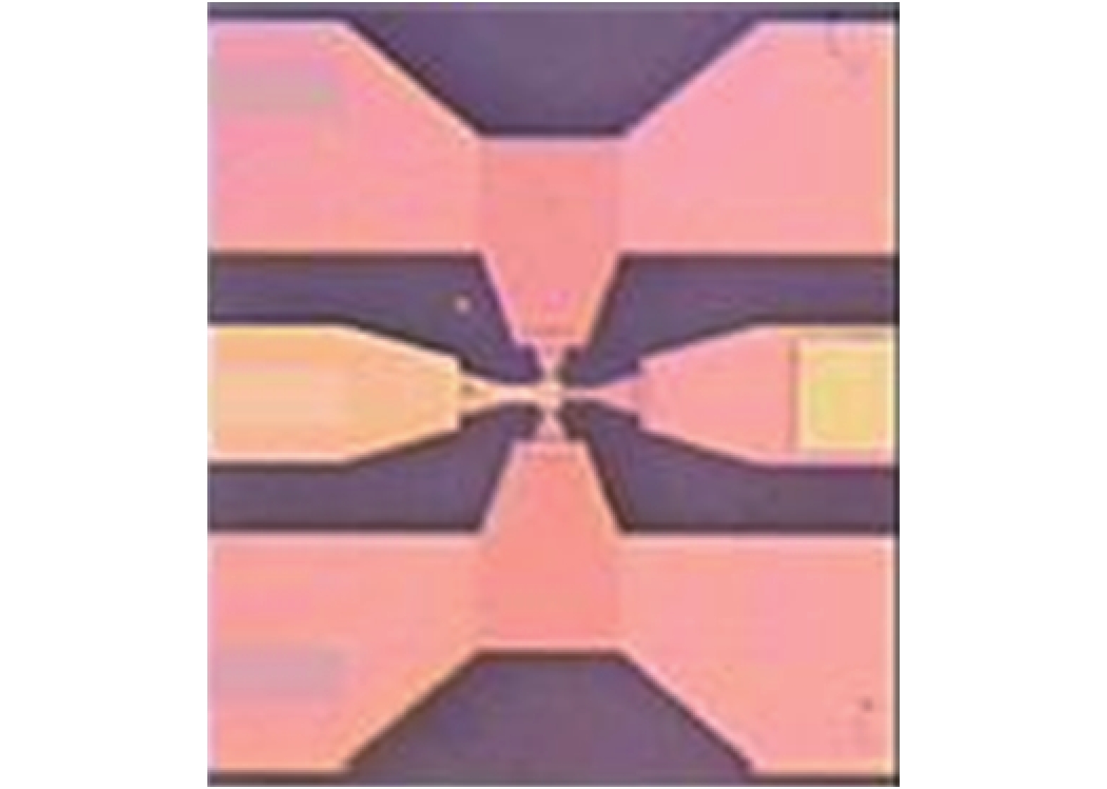
Abstract: An improved large signal model for InP HEMTs is proposed in this paper. The channel current and charge model equations are constructed based on the Angelov model equations. Both the equations for channel current and gate charge models were all continuous and high order drivable, and the proposed gate charge model satisfied the charge conservation. For the strong leakage induced barrier reduction effect of InP HEMTs, the Angelov current model equations are improved. The channel current model could fit DC performance of devices. A 2 × 25 μm × 70 nm InP HEMT device is used to demonstrate the extraction and validation of the model, in which the model has predicted the DC I–V, C–V and bias related S parameters accurately.
Key words: InP HEMT, large-signal, model
| [1] |
Lai R, Mei X B, Deal W R, et al. Sub 50 nm InP HEMT device with Fmax greater than 1 THz. IEEE International Electron Devices Meeting, 2007: 609 doi: 10.1109/IEDM.2007.4419013
|
| [2] |
Khan M A, Bhattarai A, Kuznia J N, et al. High electron mobility transistor based on a GaN–AlxGa1–xN heterojunction. Appl Phys Lett, 1993, 63(09): 1214 doi: 10.1063/1.109775
|
| [3] |
Schreurs D, Baeyens Y, Van der Zanden K, et al. Large-signal HEMT modelling, specifically optimized for InP based HEMTs. Indium Phosphide and Related Materials, 1996: 638
|
| [4] |
Radisic V, Leong M K, Mei X, et al. A 50 mW 220 GHz power amplifier module. IEEE MTT-S International Microwave Symposium Digest, 2010: 45 doi: 10.1109/MWSYM.2010.5515248
|
| [5] |
Lai R, Mei X B, Deal W R, et al. Sub 50 nm InP HEMT device with Fmax greater than 1 THz. IEEE International Electron Devices Meeting, 2007: 609
|
| [6] |
Kim T W, Kim D H, Alamo J. 60 nm self-aligned-gate InGaAs HEMTs with record high-frequency characteristics. IEEE International Electron Devices Meeting, 2010: 30 doi: 10.1109/IEDM.2010.5703454
|
| [7] |
Miyajima Y, Nukariya T, Suzuki S. Terahertz detector using 70-nm T-gate InAlAs/InGaAs HEMT integrated with bow-tie antenna. 39th International Conference on Infrared, Millimeter, and Terahertz Waves, 2014: 1 doi: 10.1109/IRMMW-THz.2014.6956520
|
| [8] |
Curtice W R, Ettenberg M. A nonlinear GaAs FET model for use in the design of output circuits for power amplifiers. IEEE Trans Microw Theory Tech, 1985, 33(12): 1383 doi: 10.1109/TMTT.1985.1133229
|
| [9] |
Statz H, Newman P, Smith I W, et al. GaAs FET device and circuit simulation in SPICE. IEEE Trans Electron Devices, 1987, 34(2): 160 doi: 10.1109/T-ED.1987.22902
|
| [10] |
Angelov I, Zirath H, Rosman N. A new empirical nonlinear model for HEMT and MESFET devices. IEEE Trans Microw Theory Tech, 1992, 40(12): 2258 doi: 10.1109/22.179888
|
| [11] |
Agilent Technologies, ICCAP Software Documentation. Palo Alto, CA: Agilent Technologies Inc., 2009
|
| [12] |
Liu Y, Reese E. AlGaN/GaN HEMT large signal nonlinear compact model accounting for thermal effects and trapping dispersion. IEEE Compound Semiconductor Integrated Circuit Symposium, 2013: 1 doi: 10.1109/CSICS.2013.6659214
|
| [13] |
Tarazi J, Schwitter B K, Parker A E, et al. AlGaN/GaN HEMT nonlinear model fitting including a trap model. IEEE MTT-S International Microwave Symposium, 2015: 1 doi: 10.1109/MWSYM.2015.7167138
|
| [14] |
King J B, Brazil T J. Nonlinear electrothermal GaN HEMT model applied to high-efficiency power amplifier design. IEEE Trans Microw Theory Tech, 2013, 61(1): 444 doi: 10.1109/TMTT.2012.2229712
|
| [15] |
Hajji R, Poulton M, Crittenden D B, et al. GaN-HEMT nonlinear modeling of single-ended and Doherty high-power amplifiers. 44th European Microwave Integrated Circuit Conference, 2014: 1317 doi: 10.1109/EuMC.2014.6986686
|
| [16] |
Marcoux N L, Fisher C J, White D, et al. A new GaN HEMT nonlinear model for evaluation and design of 1–2 watt power amplifiers. IEEE 55th International Midwest Symposium on Circuits and Systems, 2012: 53 doi: 10.1109/MWSCAS.2012.6291955
|
| [17] |
Gao J J. RF and microwave modeling and measurement techniques for field effect transistors. IET Digital Library, 2010: 268
|
| [18] |
Strahle S, Geiger D, Henle B, et al. Drift region characteristics of InP-based HEMT devices evaluated by a simple drift region model. Proceedings of 1994 IEEE 6th International Conference on Indium Phosphide and Related Materials (IPRM), 1994: 327
|
| [19] |
Schreurs D, Verspecht J, Vandenberghe S, et al. Advanced non-linear InP HEMT model parameter estimation from vectorial large-signal measurements. Eleventh International Conference on Indium Phosphide and Related Materials, 1999: 459 doi: 10.1109/ICIPRM.1999.773732
|
| [20] |
Bengtsson L, Garcia M, Karisson C, et al. Characterization and large signal modeling of InP HEMT devices. 25th European Microwave Conference, Bologna, Italy, 1995: 1168 doi: 10.1109/EUMA.1995.337148
|
| [21] |
Schreurs D, Baeyens Y, Van der Zanden K, et al. Large-signal HEMT modelling, specifically optimized for InP based HEMTs. Eighth International Conference on Indium Phosphide and Related Materials, Schwabisch-Gmund, Germany, 1996: 638 doi: 10.1109/ICIPRM.1996.492330
|
| [22] |
Schreurs D, Meer H V, Zanden K V D, et al. Improved HEMT model for low phase-noise InP-based MMIC oscillators. IEEE Trans Microw Theory Tech, 1998, 46(10): 1583 doi: 10.1109/22.721169
|
| [23] |
Schreurs D, Meer H V, Van der Zanden K, et al. Scaleable non-linear and bias-dependent low-frequency noise model for improved InP HEMT based MMIC oscillator design. Workshop on High Performance Electron Devices for Microwave and Optoelectronic Applications, 2002: 187 doi: 10.1109/EDMO.1997.668597
|
| [24] |
Guan L, Christou A, Halkias G, et al. Modeling of current-voltage characteristics for strained and lattice matched HEMT's on InP substrate using a variational charge control model. IEEE Trans Electron Devices, 1995, 42(4): 612 doi: 10.1109/16.372062
|
| [25] |
Han C J, Ruden P P, Grider D, et al. Short channel effects in submicron self-aligned gate heterostructure field effect transistors. International Electron Devices Meeting, 1988: 696
|
| [26] |
Liu Y N, Du G W, Hu Z D, et al. Study of terahertz InP HEMT device. Semicond Technol, 2016, 41(8): 599
|
| [27] |
Arora N. MOSFET modeling for VLSI simulation: theory and practice. New Jersey: World Scientific, 2007
|
| [28] |
Angelov I, Bengtsson L, Garcia M. Extensions of the chalmers nonlinear HEMT and MESFET model. IEEE Trans Microw Theory Tech, 1996, 44(10): 1664 doi: 10.1109/22.538957
|
| [29] |
Alt A R, Marti D, Bolognesi C R. Transistor modeling: robust small-signal equivalent circuit extraction in various HEMT technologies. IEEE Microwave Mag, 2013, 14(4): 83 doi: 10.1109/MMM.2013.2248593
|
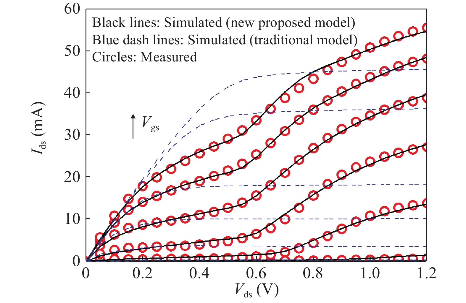
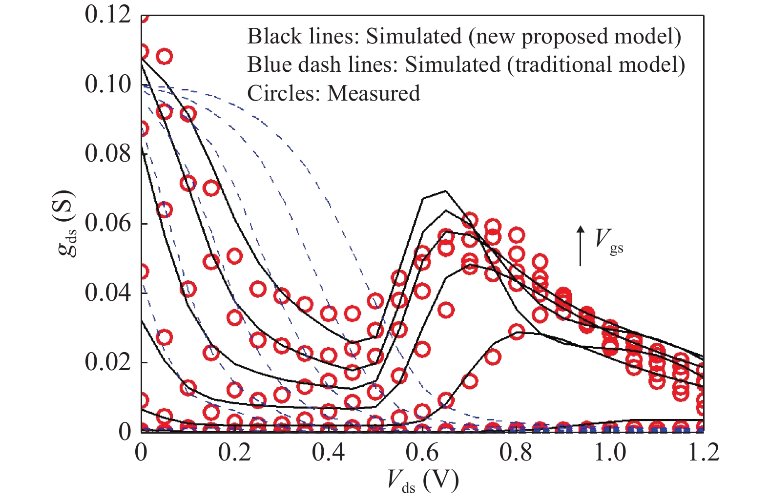
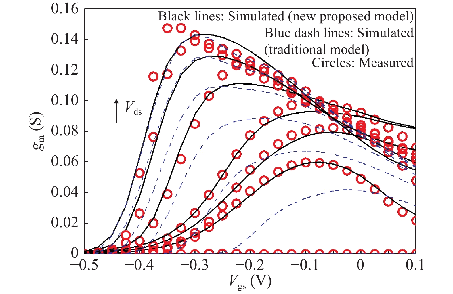
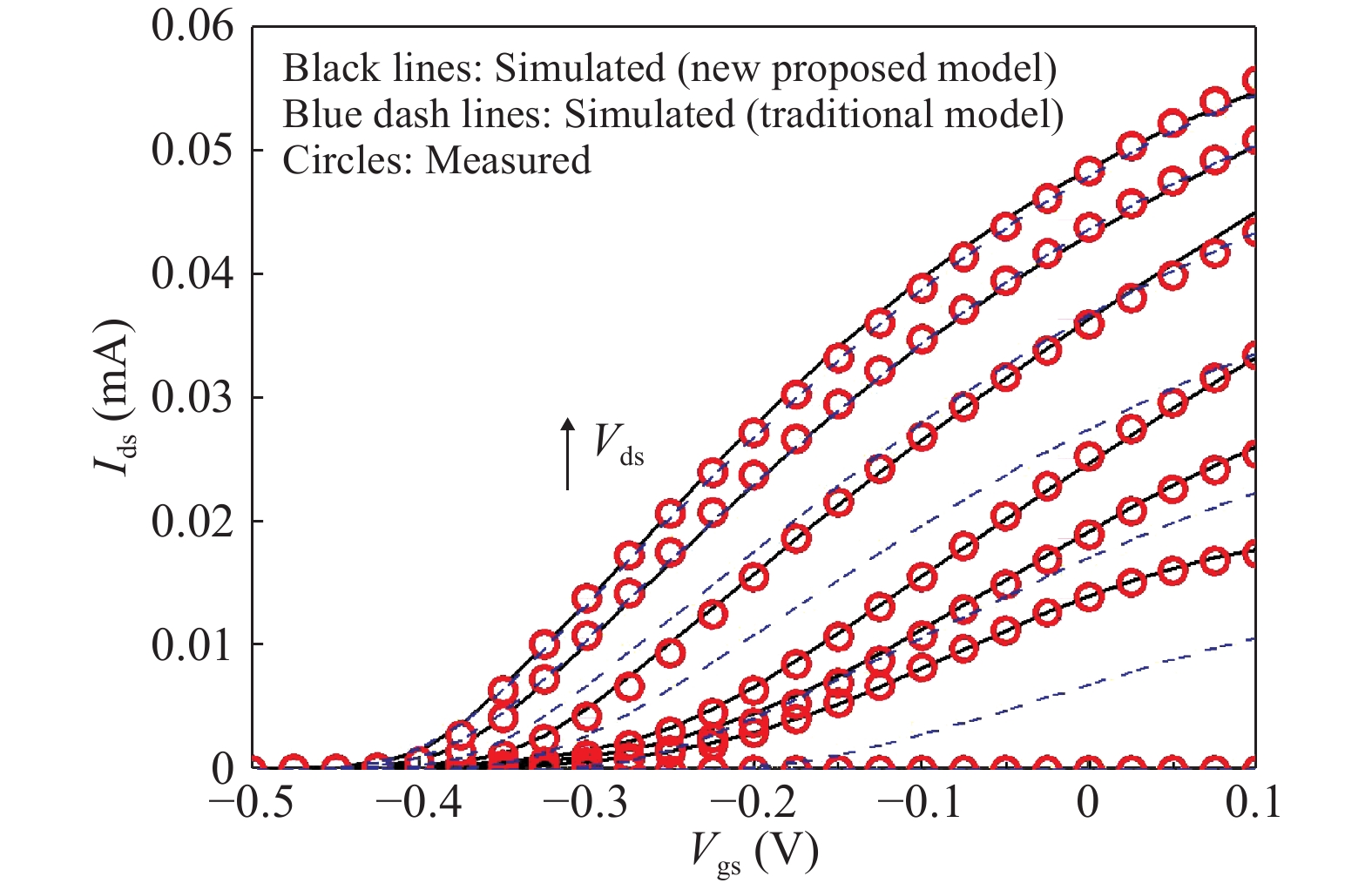
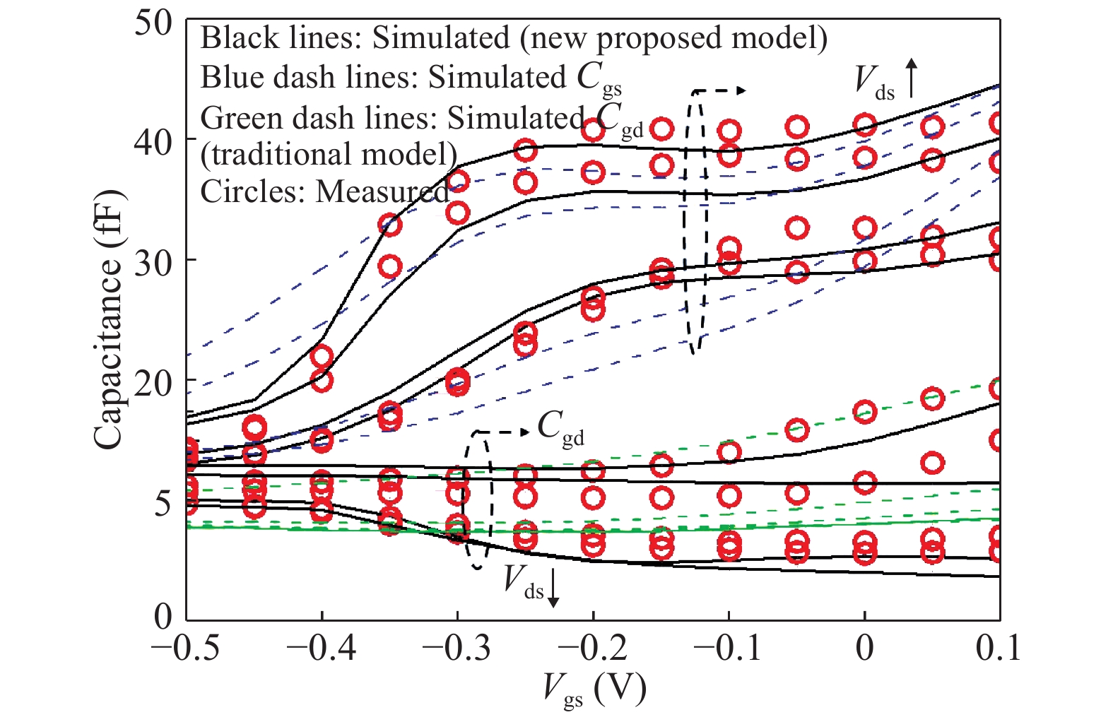
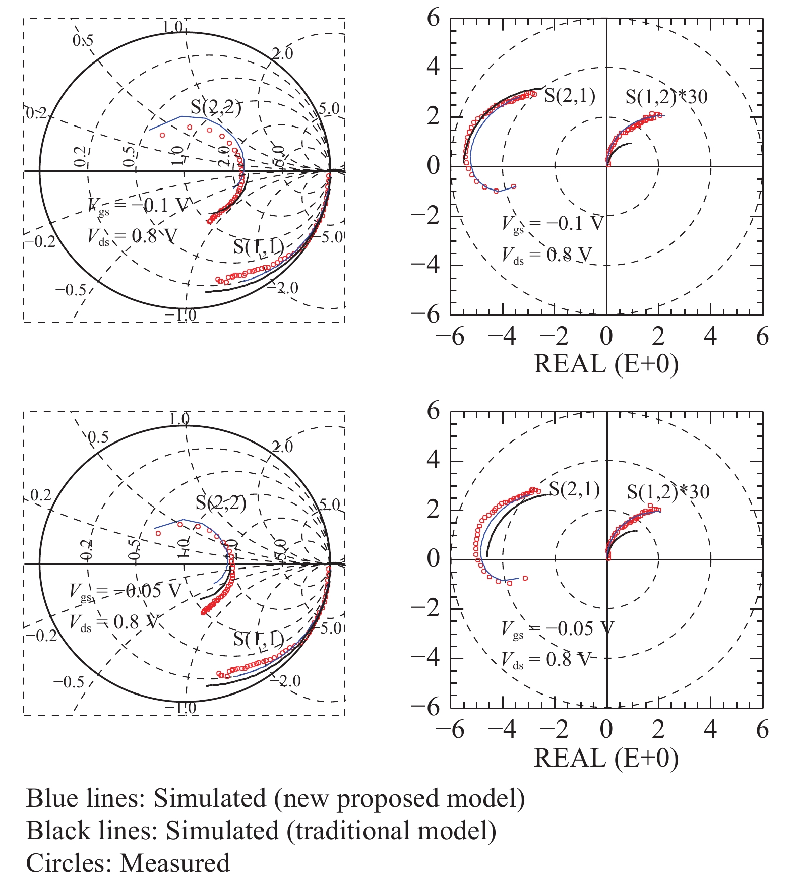
Table 2. Extracted terminal charges model parameter values from a 2-finger InP HEMT.
| Parameter | Value | Parameter | Value | ||
| P10 | 1.761 | P40 | 0.9383 | ||
| P11 | 7.353 | P41 | 3.108 | ||
| P111 | 0.1626 | Cgs0 | 1.720 fF | ||
| P20 | 0.2277 | Cgdi | 9.869 fF | ||
| P21 | 0.9625 | Cgd0 | 6.456 fF | ||
| P30 | 1.275 | Cgdi | 0.2882 fF | ||
| P31 | 0.9696 |
 DownLoad: CSV
Table 1. Extracted drain current model parameter values from a 2-finger InP HEMT.
| Parameter | Value | Parameter | Value | ||
| Ipk0a | 3.264 mA | Ipk0b | 0.010 81 mA | ||
| Vpks_a | −280.7 mV | Vpks_b | −378.8 mV | ||
| Dvpks_a | −183.5 mV | Dvpks_b | −1.152 V | ||
| P1a | 0.6875 | P1b | 0.9929 | ||
| P2a | 0.2338 | P2b | 0.4749 | ||
| P3a | 0.4857 | P3b | 0.6076 | ||
| Alphar_a | 13.58 | Alphar_b | 2.111 | ||
| Alphas_a | 0.045 07 | Alphas_b | 2.194 | ||
| Vkna | 1.0 V | Vknb | 1.0 V | ||
| Vtra | 50.0 V | Vtrb | 50.0 V | ||
| Lambda_a | 2.467 | Lambda_b | 0.4419 | ||
| Lambda1_a | 0.004 526 | Lambda1_b | 0.067 31 | ||
| B1a | 1.852 | B1b | 2.882 | ||
| B2a | 0.1618 | B2b | 0.072 43 |
DownLoad: CSV
| [1] |
Lai R, Mei X B, Deal W R, et al. Sub 50 nm InP HEMT device with Fmax greater than 1 THz. IEEE International Electron Devices Meeting, 2007: 609 doi: 10.1109/IEDM.2007.4419013
|
| [2] |
Khan M A, Bhattarai A, Kuznia J N, et al. High electron mobility transistor based on a GaN–AlxGa1–xN heterojunction. Appl Phys Lett, 1993, 63(09): 1214 doi: 10.1063/1.109775
|
| [3] |
Schreurs D, Baeyens Y, Van der Zanden K, et al. Large-signal HEMT modelling, specifically optimized for InP based HEMTs. Indium Phosphide and Related Materials, 1996: 638
|
| [4] |
Radisic V, Leong M K, Mei X, et al. A 50 mW 220 GHz power amplifier module. IEEE MTT-S International Microwave Symposium Digest, 2010: 45 doi: 10.1109/MWSYM.2010.5515248
|
| [5] |
Lai R, Mei X B, Deal W R, et al. Sub 50 nm InP HEMT device with Fmax greater than 1 THz. IEEE International Electron Devices Meeting, 2007: 609
|
| [6] |
Kim T W, Kim D H, Alamo J. 60 nm self-aligned-gate InGaAs HEMTs with record high-frequency characteristics. IEEE International Electron Devices Meeting, 2010: 30 doi: 10.1109/IEDM.2010.5703454
|
| [7] |
Miyajima Y, Nukariya T, Suzuki S. Terahertz detector using 70-nm T-gate InAlAs/InGaAs HEMT integrated with bow-tie antenna. 39th International Conference on Infrared, Millimeter, and Terahertz Waves, 2014: 1 doi: 10.1109/IRMMW-THz.2014.6956520
|
| [8] |
Curtice W R, Ettenberg M. A nonlinear GaAs FET model for use in the design of output circuits for power amplifiers. IEEE Trans Microw Theory Tech, 1985, 33(12): 1383 doi: 10.1109/TMTT.1985.1133229
|
| [9] |
Statz H, Newman P, Smith I W, et al. GaAs FET device and circuit simulation in SPICE. IEEE Trans Electron Devices, 1987, 34(2): 160 doi: 10.1109/T-ED.1987.22902
|
| [10] |
Angelov I, Zirath H, Rosman N. A new empirical nonlinear model for HEMT and MESFET devices. IEEE Trans Microw Theory Tech, 1992, 40(12): 2258 doi: 10.1109/22.179888
|
| [11] |
Agilent Technologies, ICCAP Software Documentation. Palo Alto, CA: Agilent Technologies Inc., 2009
|
| [12] |
Liu Y, Reese E. AlGaN/GaN HEMT large signal nonlinear compact model accounting for thermal effects and trapping dispersion. IEEE Compound Semiconductor Integrated Circuit Symposium, 2013: 1 doi: 10.1109/CSICS.2013.6659214
|
| [13] |
Tarazi J, Schwitter B K, Parker A E, et al. AlGaN/GaN HEMT nonlinear model fitting including a trap model. IEEE MTT-S International Microwave Symposium, 2015: 1 doi: 10.1109/MWSYM.2015.7167138
|
| [14] |
King J B, Brazil T J. Nonlinear electrothermal GaN HEMT model applied to high-efficiency power amplifier design. IEEE Trans Microw Theory Tech, 2013, 61(1): 444 doi: 10.1109/TMTT.2012.2229712
|
| [15] |
Hajji R, Poulton M, Crittenden D B, et al. GaN-HEMT nonlinear modeling of single-ended and Doherty high-power amplifiers. 44th European Microwave Integrated Circuit Conference, 2014: 1317 doi: 10.1109/EuMC.2014.6986686
|
| [16] |
Marcoux N L, Fisher C J, White D, et al. A new GaN HEMT nonlinear model for evaluation and design of 1–2 watt power amplifiers. IEEE 55th International Midwest Symposium on Circuits and Systems, 2012: 53 doi: 10.1109/MWSCAS.2012.6291955
|
| [17] |
Gao J J. RF and microwave modeling and measurement techniques for field effect transistors. IET Digital Library, 2010: 268
|
| [18] |
Strahle S, Geiger D, Henle B, et al. Drift region characteristics of InP-based HEMT devices evaluated by a simple drift region model. Proceedings of 1994 IEEE 6th International Conference on Indium Phosphide and Related Materials (IPRM), 1994: 327
|
| [19] |
Schreurs D, Verspecht J, Vandenberghe S, et al. Advanced non-linear InP HEMT model parameter estimation from vectorial large-signal measurements. Eleventh International Conference on Indium Phosphide and Related Materials, 1999: 459 doi: 10.1109/ICIPRM.1999.773732
|
| [20] |
Bengtsson L, Garcia M, Karisson C, et al. Characterization and large signal modeling of InP HEMT devices. 25th European Microwave Conference, Bologna, Italy, 1995: 1168 doi: 10.1109/EUMA.1995.337148
|
| [21] |
Schreurs D, Baeyens Y, Van der Zanden K, et al. Large-signal HEMT modelling, specifically optimized for InP based HEMTs. Eighth International Conference on Indium Phosphide and Related Materials, Schwabisch-Gmund, Germany, 1996: 638 doi: 10.1109/ICIPRM.1996.492330
|
| [22] |
Schreurs D, Meer H V, Zanden K V D, et al. Improved HEMT model for low phase-noise InP-based MMIC oscillators. IEEE Trans Microw Theory Tech, 1998, 46(10): 1583 doi: 10.1109/22.721169
|
| [23] |
Schreurs D, Meer H V, Van der Zanden K, et al. Scaleable non-linear and bias-dependent low-frequency noise model for improved InP HEMT based MMIC oscillator design. Workshop on High Performance Electron Devices for Microwave and Optoelectronic Applications, 2002: 187 doi: 10.1109/EDMO.1997.668597
|
| [24] |
Guan L, Christou A, Halkias G, et al. Modeling of current-voltage characteristics for strained and lattice matched HEMT's on InP substrate using a variational charge control model. IEEE Trans Electron Devices, 1995, 42(4): 612 doi: 10.1109/16.372062
|
| [25] |
Han C J, Ruden P P, Grider D, et al. Short channel effects in submicron self-aligned gate heterostructure field effect transistors. International Electron Devices Meeting, 1988: 696
|
| [26] |
Liu Y N, Du G W, Hu Z D, et al. Study of terahertz InP HEMT device. Semicond Technol, 2016, 41(8): 599
|
| [27] |
Arora N. MOSFET modeling for VLSI simulation: theory and practice. New Jersey: World Scientific, 2007
|
| [28] |
Angelov I, Bengtsson L, Garcia M. Extensions of the chalmers nonlinear HEMT and MESFET model. IEEE Trans Microw Theory Tech, 1996, 44(10): 1664 doi: 10.1109/22.538957
|
| [29] |
Alt A R, Marti D, Bolognesi C R. Transistor modeling: robust small-signal equivalent circuit extraction in various HEMT technologies. IEEE Microwave Mag, 2013, 14(4): 83 doi: 10.1109/MMM.2013.2248593
|


Article views: 4622 Times PDF downloads: 108 Times Cited by: 0 Times
Received: 14 September 2017 Revised: 11 November 2017 Online: Accepted Manuscript: 19 January 2018Uncorrected proof: 24 January 2018Published: 01 May 2018
| Citation: |
Tianhao Li, Wenjun Li, Jun Liu. An improved large signal model of InP HEMTs[J]. Journal of Semiconductors, 2018, 39(5): 054003. doi: 10.1088/1674-4926/39/5/054003
T H Li, W J Li, J Liu. An improved large signal model of InP HEMTs[J]. J. Semicond., 2018, 39(5): 054003. doi: 10.1088/1674-4926/39/5/054003.
Export: BibTex EndNote

|
| [1] |
Lai R, Mei X B, Deal W R, et al. Sub 50 nm InP HEMT device with Fmax greater than 1 THz. IEEE International Electron Devices Meeting, 2007: 609 doi: 10.1109/IEDM.2007.4419013
|
| [2] |
Khan M A, Bhattarai A, Kuznia J N, et al. High electron mobility transistor based on a GaN–AlxGa1–xN heterojunction. Appl Phys Lett, 1993, 63(09): 1214 doi: 10.1063/1.109775
|
| [3] |
Schreurs D, Baeyens Y, Van der Zanden K, et al. Large-signal HEMT modelling, specifically optimized for InP based HEMTs. Indium Phosphide and Related Materials, 1996: 638
|
| [4] |
Radisic V, Leong M K, Mei X, et al. A 50 mW 220 GHz power amplifier module. IEEE MTT-S International Microwave Symposium Digest, 2010: 45 doi: 10.1109/MWSYM.2010.5515248
|
| [5] |
Lai R, Mei X B, Deal W R, et al. Sub 50 nm InP HEMT device with Fmax greater than 1 THz. IEEE International Electron Devices Meeting, 2007: 609
|
| [6] |
Kim T W, Kim D H, Alamo J. 60 nm self-aligned-gate InGaAs HEMTs with record high-frequency characteristics. IEEE International Electron Devices Meeting, 2010: 30 doi: 10.1109/IEDM.2010.5703454
|
| [7] |
Miyajima Y, Nukariya T, Suzuki S. Terahertz detector using 70-nm T-gate InAlAs/InGaAs HEMT integrated with bow-tie antenna. 39th International Conference on Infrared, Millimeter, and Terahertz Waves, 2014: 1 doi: 10.1109/IRMMW-THz.2014.6956520
|
| [8] |
Curtice W R, Ettenberg M. A nonlinear GaAs FET model for use in the design of output circuits for power amplifiers. IEEE Trans Microw Theory Tech, 1985, 33(12): 1383 doi: 10.1109/TMTT.1985.1133229
|
| [9] |
Statz H, Newman P, Smith I W, et al. GaAs FET device and circuit simulation in SPICE. IEEE Trans Electron Devices, 1987, 34(2): 160 doi: 10.1109/T-ED.1987.22902
|
| [10] |
Angelov I, Zirath H, Rosman N. A new empirical nonlinear model for HEMT and MESFET devices. IEEE Trans Microw Theory Tech, 1992, 40(12): 2258 doi: 10.1109/22.179888
|
| [11] |
Agilent Technologies, ICCAP Software Documentation. Palo Alto, CA: Agilent Technologies Inc., 2009
|
| [12] |
Liu Y, Reese E. AlGaN/GaN HEMT large signal nonlinear compact model accounting for thermal effects and trapping dispersion. IEEE Compound Semiconductor Integrated Circuit Symposium, 2013: 1 doi: 10.1109/CSICS.2013.6659214
|
| [13] |
Tarazi J, Schwitter B K, Parker A E, et al. AlGaN/GaN HEMT nonlinear model fitting including a trap model. IEEE MTT-S International Microwave Symposium, 2015: 1 doi: 10.1109/MWSYM.2015.7167138
|
| [14] |
King J B, Brazil T J. Nonlinear electrothermal GaN HEMT model applied to high-efficiency power amplifier design. IEEE Trans Microw Theory Tech, 2013, 61(1): 444 doi: 10.1109/TMTT.2012.2229712
|
| [15] |
Hajji R, Poulton M, Crittenden D B, et al. GaN-HEMT nonlinear modeling of single-ended and Doherty high-power amplifiers. 44th European Microwave Integrated Circuit Conference, 2014: 1317 doi: 10.1109/EuMC.2014.6986686
|
| [16] |
Marcoux N L, Fisher C J, White D, et al. A new GaN HEMT nonlinear model for evaluation and design of 1–2 watt power amplifiers. IEEE 55th International Midwest Symposium on Circuits and Systems, 2012: 53 doi: 10.1109/MWSCAS.2012.6291955
|
| [17] |
Gao J J. RF and microwave modeling and measurement techniques for field effect transistors. IET Digital Library, 2010: 268
|
| [18] |
Strahle S, Geiger D, Henle B, et al. Drift region characteristics of InP-based HEMT devices evaluated by a simple drift region model. Proceedings of 1994 IEEE 6th International Conference on Indium Phosphide and Related Materials (IPRM), 1994: 327
|
| [19] |
Schreurs D, Verspecht J, Vandenberghe S, et al. Advanced non-linear InP HEMT model parameter estimation from vectorial large-signal measurements. Eleventh International Conference on Indium Phosphide and Related Materials, 1999: 459 doi: 10.1109/ICIPRM.1999.773732
|
| [20] |
Bengtsson L, Garcia M, Karisson C, et al. Characterization and large signal modeling of InP HEMT devices. 25th European Microwave Conference, Bologna, Italy, 1995: 1168 doi: 10.1109/EUMA.1995.337148
|
| [21] |
Schreurs D, Baeyens Y, Van der Zanden K, et al. Large-signal HEMT modelling, specifically optimized for InP based HEMTs. Eighth International Conference on Indium Phosphide and Related Materials, Schwabisch-Gmund, Germany, 1996: 638 doi: 10.1109/ICIPRM.1996.492330
|
| [22] |
Schreurs D, Meer H V, Zanden K V D, et al. Improved HEMT model for low phase-noise InP-based MMIC oscillators. IEEE Trans Microw Theory Tech, 1998, 46(10): 1583 doi: 10.1109/22.721169
|
| [23] |
Schreurs D, Meer H V, Van der Zanden K, et al. Scaleable non-linear and bias-dependent low-frequency noise model for improved InP HEMT based MMIC oscillator design. Workshop on High Performance Electron Devices for Microwave and Optoelectronic Applications, 2002: 187 doi: 10.1109/EDMO.1997.668597
|
| [24] |
Guan L, Christou A, Halkias G, et al. Modeling of current-voltage characteristics for strained and lattice matched HEMT's on InP substrate using a variational charge control model. IEEE Trans Electron Devices, 1995, 42(4): 612 doi: 10.1109/16.372062
|
| [25] |
Han C J, Ruden P P, Grider D, et al. Short channel effects in submicron self-aligned gate heterostructure field effect transistors. International Electron Devices Meeting, 1988: 696
|
| [26] |
Liu Y N, Du G W, Hu Z D, et al. Study of terahertz InP HEMT device. Semicond Technol, 2016, 41(8): 599
|
| [27] |
Arora N. MOSFET modeling for VLSI simulation: theory and practice. New Jersey: World Scientific, 2007
|
| [28] |
Angelov I, Bengtsson L, Garcia M. Extensions of the chalmers nonlinear HEMT and MESFET model. IEEE Trans Microw Theory Tech, 1996, 44(10): 1664 doi: 10.1109/22.538957
|
| [29] |
Alt A R, Marti D, Bolognesi C R. Transistor modeling: robust small-signal equivalent circuit extraction in various HEMT technologies. IEEE Microwave Mag, 2013, 14(4): 83 doi: 10.1109/MMM.2013.2248593
|

 WeChat ID
Journal of Semiconductors © 2017 All Rights Reserved 京ICP备05085259号-2