| [1] |
Fleischmann M, Hendra P J, McQuillan A J. Raman spectra of pyridine adsorbed at a silver electrode. Chem Phys Lett, 1974, 26, 163 doi: 10.1016/0009-2614(74)85388-1 |
| [2] |
Chen N, Xiao T H, Luo Z, et al. Porous carbon nanowire array for surface-enhanced Raman spectroscopy. Nat Commun, 2020, 11, 4772 doi: 10.1038/s41467-020-18590-7 |
| [3] |
Wei X P, Su S, Guo Y Y, et al. A molecular beacon-based signal-off surface-enhanced Raman scattering strategy for highly sensitive, reproducible, and multiplexed DNA detection. Small, 2013, 9, 2493 doi: 10.1002/smll.201202914 |
| [4] |
Srichan C, Ekpanyapong M, Horprathum M, et al. Highly-sensitive surface-enhanced Raman spectroscopy (SERS)-based chemical sensor using 3D graphene foam decorated with silver nanoparticles as SERS substrate. Sci Rep, 2016, 6, 23733 doi: 10.1038/srep23733 |
| [5] |
Campion A, Kambhampati P. Surface-enhanced Raman scattering. Chem Soc Rev, 1998, 27, 241 doi: 10.1039/a827241z |
| [6] |
Shan Y F, Zheng Z H, Liu J J, et al. Niobium pentoxide: A promising surface-enhanced Raman scattering active semiconductor substrate. npj Comput Mater, 2017, 3, 11 doi: 10.1038/s41524-017-0008-0 |
| [7] |
Ding S Y, Yi J, Li J F, et al. Nanostructure-based plasmon-enhanced Raman spectroscopy for surface analysis of materials. Nat Rev Mater, 2016, 1, 16021 doi: 10.1038/natrevmats.2016.21 |
| [8] |
Pieczonka N P, Aroca R F. Single molecule analysis by surfaced-enhanced Raman scattering. Chem Soc Rev, 2008, 37, 946 doi: 10.1039/b709739p |
| [9] |
Haldavnekar R, Venkatakrishnan K, Tan B. Non plasmonic semiconductor quantum SERS probe as a pathway for in vitro cancer detection. Nat Commun, 2018, 9, 3065 doi: 10.1038/s41467-018-05237-x |
| [10] |
Rickard J J S, Di-Pietro V, Smith D J, et al. Rapid optofluidic detection of biomarkers for traumatic brain injury via surface-enhanced Raman spectroscopy. Nat Biomed Eng, 2020, 4, 610 doi: 10.1038/s41551-019-0510-4 |
| [11] |
Fraser J P, Postnikov P, Miliutina E, et al. Application of a 2D molybdenum telluride in SERS detection of biorelevant molecules. ACS Appl Mater Interfaces, 2020, 12, 47774 doi: 10.1021/acsami.0c11231 |
| [12] |
Pham T B, Hoang T H C, Pham V H, et al. Detection of Permethrin pesticide using silver nano-dendrites SERS on optical fibre fabricated by laser-assisted photochemical method. Sci Rep, 2019, 9, 12590 doi: 10.1038/s41598-019-49077-1 |
| [13] |
Shi G C, Wang M L, Zhu Y Y, et al. Dragonfly wing decorated by gold nanoislands as flexible and stable substrates for surface-enhanced Raman scattering (SERS). Sci Rep, 2018, 8, 6916 doi: 10.1038/s41598-018-25228-8 |
| [14] |
Satheeshkumar E, Makaryan T, Melikyan A, et al. One-step solution processing of Ag, Au and Pd@MXene hybrids for SERS. Sci Rep, 2016, 6, 32049 doi: 10.1038/srep32049 |
| [15] |
Campion A, Ivanecky J E III, Child C M, et al. On the mechanism of chemical enhancement in surface-enhanced Raman scattering. J Am Chem Soc, 1995, 117, 11807 doi: 10.1021/ja00152a024 |
| [16] |
Tan Y, Ma L N, Gao Z B, et al. Two-dimensional heterostructure as a platform for surface-enhanced Raman scattering. Nano Lett, 2017, 17, 2621 doi: 10.1021/acs.nanolett.7b00412 |
| [17] |
Feng S, Dos Santos M C, Carvalho B R, et al. Ultrasensitive molecular sensor using N-doped graphene through enhanced Raman scattering. Sci Adv, 2016, 2, e1600322 doi: 10.1126/sciadv.1600322 |
| [18] |
Yang M, Alvarez-Puebla R, Kim H S, et al. SERS-active gold lace nanoshells with built-in hotspots. Nano Lett, 2010, 10, 4013 doi: 10.1021/nl101946c |
| [19] |
Karthick Kannan P, Shankar P, Blackman C, et al. Recent advances in 2D inorganic nanomaterials for SERS sensing. Adv Mater, 2019, 31, 1803432 doi: 10.1002/adma.201803432 |
| [20] |
Kleinman S L, Sharma B, Blaber M G, et al. Structure enhancement factor relationships in single gold nanoantennas by surface-enhanced Raman excitation spectroscopy. J Am Chem Soc, 2013, 135, 301 doi: 10.1021/ja309300d |
| [21] |
Wustholz K L, Henry A I, McMahon J M, et al. Structure–activity relationships in gold nanoparticle dimers and trimers for surface-enhanced Raman spectroscopy. J Am Chem Soc, 2010, 132, 10903 doi: 10.1021/ja104174m |
| [22] |
Maher R C, Cohen L F, Le Ru E C, et al. A study of local heating of molecules under surface enhanced Raman scattering (SERS) conditions using the anti-Stokes/Stokes ratio. Faraday Discuss, 2006, 132, 77 doi: 10.1039/B510413K |
| [23] |
Schatz G C, Young M A, Duyne R P. Electromagnetic mechanism of SERS. Springer, 2006
|
| [24] |
Kim J, Jang Y, Kim N J, et al. Study of chemical enhancement mechanism in non-plasmonic surface enhanced Raman spectroscopy (SERS). Front Chem, 2019, 7, 582 doi: 10.3389/fchem.2019.00582 |
| [25] |
Ling X, Moura L G, Pimenta M A, et al. Charge-transfer mechanism in graphene-enhanced Raman scattering. J Phys Chem C, 2012, 116, 25112 doi: 10.1021/jp3088447 |
| [26] |
Ling X, Wu J X, Xu W G, et al. Probing the effect of molecular orientation on the intensity of chemical enhancement using graphene-enhanced Raman spectroscopy. Small, 2012, 8, 1365 doi: 10.1002/smll.201102223 |
| [27] |
Lin J, Shang Y, Li X X, et al. Ultrasensitive SERS detection by defect engineering on single Cu 2O superstructure particle. Adv Mater, 2017, 29, 1604797 doi: 10.1002/adma.201604797 |
| [28] |
Osawa M, Matsuda N, Yoshii K, et al. Charge transfer resonance Raman process in surface-enhanced Raman scattering from p-aminothiophenol adsorbed on silver: Herzberg-Teller contribution. J Phys Chem, 1994, 98, 12702 doi: 10.1021/j100099a038 |
| [29] |
|
| [30] |
Lombardi J R, Birke R L. Theory of surface-enhanced Raman scattering in semiconductors. J Phys Chem C, 2014, 118, 11120 doi: 10.1021/jp5020675 |
| [31] |
Saleh T A, Al-Shalalfeh M M, Al-Saadi A A. Silver loaded graphene as a substrate for sensing 2-thiouracil using surface-enhanced Raman scattering. Sensor Actuat B, 2018, 254, 1110 doi: 10.1016/j.snb.2017.07.179 |
| [32] |
Jiang C X, Wei Y Q, Zhao P C, et al. Investigation of surface-enhanced Raman spectroscopy on the substrates of telluride 2D material. Eur Phys J Plus, 2020, 135, 671 doi: 10.1140/epjp/s13360-020-00688-y |
| [33] |
Kitadai H, Wang X Z, Mao N N, et al. Enhanced Raman scattering on nine 2D van der waals materials. J Phys Chem Lett, 2019, 10, 3043 doi: 10.1021/acs.jpclett.9b01146 |
| [34] |
Li W W, Xiong L, Li N C, et al. Tunable 3D light trapping architectures based on self-assembled SnSe 2 nanoplate arrays for ultrasensitive SERS detection. J Mater Chem C, 2019, 7, 10179 doi: 10.1039/C9TC03715B |
| [35] |
Manzeli S, Ovchinnikov D, Pasquier D, et al. 2D transition metal dichalcogenides. Nat Rev Mater, 2017, 2, 1 doi: 10.1038/natrevmats.2017.33 |
| [36] |
Song X J, Wang Y, Zhao F, et al. Plasmon-free surface-enhanced Raman spectroscopy using metallic 2D materials. ACS Nano, 2019, 13, 8312 doi: 10.1021/acsnano.9b03761 |
| [37] |
Zhang N, Lin J J, Zhang S Q, et al. Doping modulated in-plane anisotropic Raman enhancement on layered ReS 2. Nano Res, 2019, 12, 563 doi: 10.1007/s12274-018-2254-y |
| [38] |
Chen M P, Liu D, Du X Y, et al. 2D materials: Excellent substrates for surface-enhanced Raman scattering (SERS) in chemical sensing and biosensing. Trac Trends Anal Chem, 2020, 130, 115983 doi: 10.1016/j.trac.2020.115983 |
| [39] |
Mak K F, Shan J. Photonics and optoelectronics of 2D semiconductor transition metal dichalcogenides. Nat Photonics, 2016, 10, 216 doi: 10.1038/nphoton.2015.282 |
| [40] |
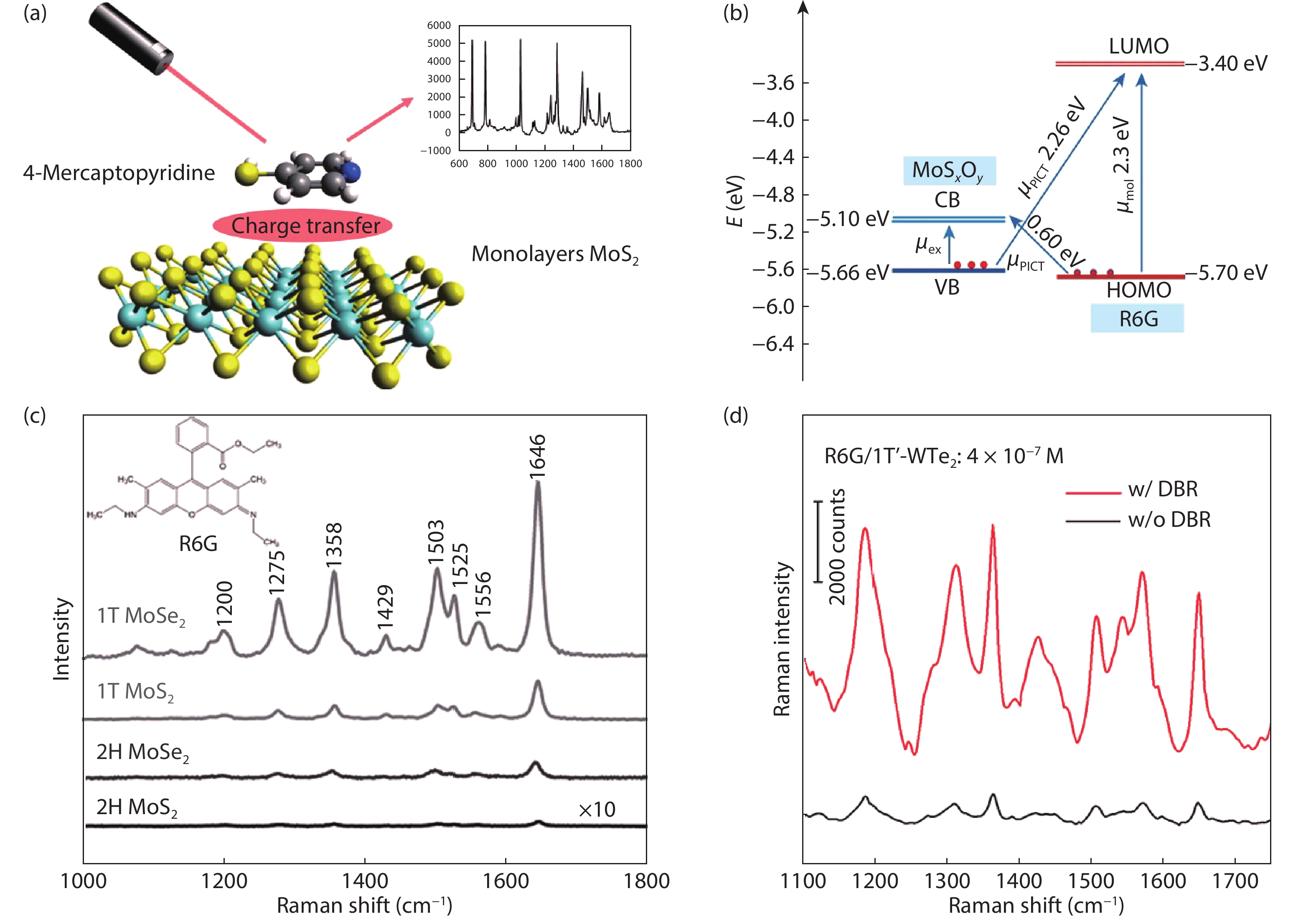
Lee Y, Kim H, Lee J, et al. Enhanced Raman scattering of rhodamine 6G films on two-dimensional transition metal dichalcogenides correlated to photoinduced charge transfer. Chem Mater, 2016, 28, 180 doi: 10.1021/acs.chemmater.5b03714 |
| [41] |
Li H, Zhang Q, Yap C C R, et al. From bulk to monolayer MoS 2: Evolution of Raman scattering. Adv Funct Mater, 2012, 22, 1385 doi: 10.1002/adfm.201102111 |
| [42] |
Li Z, Jiang S Z, Xu S C, et al. Facile synthesis of large-area and highly crystalline WS 2 film on dielectric surfaces for SERS. J Alloy Compd, 2016, 666, 412 doi: 10.1016/j.jallcom.2016.01.126 |
| [43] |
Liu Y R, Gao Z B, Chen M, et al. Enhanced Raman scattering of CuPc films on imperfect WSe 2 monolayer correlated to exciton and charge-transfer resonances. Adv Funct Mater, 2018, 28, 1805710 doi: 10.1002/adfm.201805710 |
| [44] |
Lu Z Y, Si H P, Li Z, et al. Sensitive, reproducible, and stable 3D plasmonic hybrids with bilayer WS 2 as nanospacer for SERS analysis. Opt Express, 2018, 26, 21626 doi: 10.1364/OE.26.021626 |
| [45] |
Meng L, Hu S, Xu C J, et al. Surface enhanced Raman effect on CVD growth of WS 2 film. Chem Phys Lett, 2018, 707, 71 doi: 10.1016/j.cplett.2018.07.040 |
| [46] |
Miao P, Qin J K, Shen Y F, et al. Unraveling the Raman enhancement mechanism on 1T'-phase ReS 2 nanosheets. Small, 2018, 14, 1704079 doi: 10.1002/smll.201704079 |
| [47] |
Shutov A D, Yi Z H, Wang J Z, et al. Giant chemical surface enhancement of coherent Raman scattering on MoS 2. ACS Photonics, 2018, 5, 4960 doi: 10.1021/acsphotonics.8b01136 |
| [48] |
Xu Y Y, Yang C, Jiang S Z, et al. Layer-controlled large area MoS 2 layers grown on mica substrate for surface-enhanced Raman scattering. Appl Surf Sci, 2015, 357, 1708 doi: 10.1016/j.apsusc.2015.10.032 |
| [49] |
Zheng G, Zhang P, Zhang S W, et al. SERS effect of selectively adsorbed dyes by hydrothermally-produced MoS 2 nanosheets. New J Chem, 2018, 42, 18906 doi: 10.1039/C8NJ03837F |
| [50] |
Muehlethaler C, Considine C R, Menon V, et al. Ultrahigh Raman enhancement on monolayer MoS 2. ACS Photonics, 2016, 3, 1164 doi: 10.1021/acsphotonics.6b00213 |
| [51] |
Sun L F, Hu H L, Zhan D, et al. Plasma modified MoS 2 nanoflakes for surface enhanced Raman scattering. Small, 2014, 10, 1090 doi: 10.1002/smll.201300798 |
| [52] |
Zuo P, Jiang L, Li X, et al. Enhancing charge transfer with foreign molecules through femtosecond laser induced MoS 2 defect sites for photoluminescence control and SERS enhancement. Nanoscale, 2019, 11, 485 doi: 10.1039/C8NR08785G |
| [53] |
Zheng Z, Cong S, Gong W, et al. Semiconductor SERS enhancement enabled by oxygen incorporation. Nat Commun, 2017, 8, 1993 doi: 10.1038/s41467-017-02166-z |
| [54] |
Hou X, Lin Q, Wei Y, et al. Surface-enhanced Raman scattering monitoring of oxidation states in defect-engineered two-dimensional transition metal dichalcogenides. J Phys Chem Lett, 2020, 11, 7981 doi: 10.1021/acs.jpclett.0c02318 |
| [55] |
Chen M P, Ji B, Dai Z Y, et al. Vertically-aligned 1T/2H-MS 2 (M = Mo, W) nanosheets for surface-enhanced Raman scattering with long-term stability and large-scale uniformity. Appl Surf Sci, 2020, 527, 146769 doi: 10.1016/j.apsusc.2020.146769 |
| [56] |
Er E, Hou H L, Criado A, et al. High-yield preparation of exfoliated 1T-MoS 2 with SERS activity. Chem Mater, 2019, 31, 5725 doi: 10.1021/acs.chemmater.9b01698 |
| [57] |
Yin Y, Miao P, Zhang Y M, et al. Significantly increased Raman enhancement on MoX 2 (X = S, Se) monolayers upon phase transition. Adv Funct Mater, 2017, 27, 1606694 doi: 10.1002/adfm.201606694 |
| [58] |
Tao L, Chen K, Chen Z, et al. 1T′ transition metal telluride atomic layers for plasmon-free SERS at femtomolar levels. J Am Chem Soc, 2018, 140, 8696 doi: 10.1021/jacs.8b02972 |
| [59] |
Zhang K L, Feng Y L, Wang F, et al. Two dimensional hexagonal boron nitride (2D-hBN): Synthesis, properties and applications. J Mater Chem C, 2017, 5, 11992 doi: 10.1039/C7TC04300G |
| [60] |
Giovannetti G, Khomyakov P A, Brocks G, et al. Substrate-induced band gap in graphene on hexagonal boron nitride: Ab initiodensity functional calculations. Phys Rev B, 2007, 76, 073103 doi: 10.1103/PhysRevB.76.073103 |
| [61] |
Li J, Majety S, Dahal R, et al. Dielectric strength, optical absorption, and deep ultraviolet detectors of hexagonal boron nitride epilayers. Appl Phys Lett, 2012, 101, 171112 doi: 10.1063/1.4764533 |
| [62] |
Novoselov K S, Geim A K, Morozov S V, et al. Two-dimensional gas of massless Dirac fermions in graphene. Nature, 2005, 438, 197 doi: 10.1038/nature04233 |
| [63] |
Bao J, Edwards M, Huang S R, et al. Two-dimensional hexagonal boron nitride as lateral heat spreader in electrically insulating packaging. J Phys D, 2016, 49, 265501 doi: 10.1088/0022-3727/49/26/265501 |
| [64] |
Chimene D, Alge D L, Gaharwar A K. Two-dimensional nanomaterials for biomedical applications: Emerging trends and future prospects. Adv Mater, 2015, 27, 7261 doi: 10.1002/adma.201502422 |
| [65] |
Wang J G, Ma F C, Liang W J, et al. Optical, photonic and optoelectronic properties of graphene, h-BN and their hybrid materials. Nanophotonics, 2017, 6, 943 doi: 10.1515/nanoph-2017-0015 |
| [66] |
Cai Q R, Mateti S, Yang W R, et al. Boron nitride nanosheets improve sensitivity and reusability of surface-enhanced Raman spectroscopy. Angew Chem, 2016, 128, 8545 doi: 10.1002/ange.201600517 |
| [67] |
Chugh D, Jagadish C, Tan H. Large-area hexagonal boron nitride for surface enhanced Raman spectroscopy. Adv Mater Technol, 2019, 4, 1900220 doi: 10.1002/admt.201900220 |
| [68] |
Ling X, Fang W J, Lee Y H, et al. Raman enhancement effect on two-dimensional layered materials: Graphene, h-BN and MoS 2. Nano Lett, 2014, 14, 3033 doi: 10.1021/nl404610c |
| [69] |
Liu J, Zheng T T, Tian Y. Functionalized h-BN nanosheets as a theranostic platform for SERS real-time monitoring of MicroRNA and photodynamic therapy. Angew Chem Int Ed, 2019, 58, 7757 doi: 10.1002/anie.201902776 |
| [70] |
Xia F N, Wang H, Jia Y C. Rediscovering black phosphorus as an anisotropic layered material for optoelectronics and electronics. Nat Commun, 2014, 5, 4458 doi: 10.1038/ncomms5458 |
| [71] |
Cho S Y, Lee Y, Koh H J, et al. Superior chemical sensing performance of black phosphorus: Comparison with MoS 2 and graphene. Adv Mater, 2016, 28, 7020 doi: 10.1002/adma.201601167 |
| [72] |
Ling X, Zhang J. First-layer effect in graphene-enhanced Raman scattering. Small, 2010, 6, 2020 doi: 10.1002/smll.201000918 |
| [73] |
Guo Z N, Zhang H, Lu S B, et al. From black phosphorus to phosphorene: Basic solvent exfoliation, evolution of Raman scattering, and applications to ultrafast photonics. Adv Funct Mater, 2015, 25, 6996 doi: 10.1002/adfm.201502902 |
| [74] |
Kim J, Lee J U, Lee J, et al. Correction: Anomalous polarization dependence of Raman scattering and crystallographic orientation of black phosphorus. Nanoscale, 2020, 12, 10407 doi: 10.1039/D0NR90098B |
| [75] |
Liu S J, Huo N J, Gan S, et al. Thickness-dependent Raman spectra, transport properties and infrared photoresponse of few-layer black phosphorus. J Mater Chem C, 2015, 3, 10974 doi: 10.1039/C5TC01809A |
| [76] |
Wang R, Yan X Y, Ge B C, et al. Facile preparation of self-assembled black phosphorus-dye composite films for chemical gas sensors and surface-enhanced Raman scattering performances. ACS Sustain Chem Eng, 2020, 8, 4521 doi: 10.1021/acssuschemeng.9b07840 |
| [77] |
Lu W L, Nan H Y, Hong J H, et al. Plasma-assisted fabrication of monolayer phosphorene and its Raman characterization. Nano Res, 2014, 7, 853 doi: 10.1007/s12274-014-0446-7 |
| [78] |
Liu X L, Wood J D, Chen K S, et al. In situ thermal decomposition of exfoliated two-dimensional black phosphorus. J Phys Chem Lett, 2015, 6, 773 doi: 10.1021/acs.jpclett.5b00043 |
| [79] |
Fortin-Deschênes M, Levesque P L, Martel R, et al. Dynamics and mechanisms of exfoliated black phosphorus sublimation. J Phys Chem Lett, 2016, 7, 1667 doi: 10.1021/acs.jpclett.6b00584 |
| [80] |
Kundu A, Rani R, Hazra K S. Controlled nanofabrication of metal-free SERS substrate on few layered black phosphorus by low power focused laser irradiation. Nanoscale, 2019, 11, 16245 doi: 10.1039/C9NR02615K |
| [81] |
Chenet D A, Aslan O B, Huang P Y, et al. In-plane anisotropy in mono- and few-layer ReS 2 probed by Raman spectroscopy and scanning transmission electron microscopy. Nano Lett, 2015, 15, 5667 doi: 10.1021/acs.nanolett.5b00910 |
| [82] |
Fei R X, Yang L. Strain-engineering the anisotropic electrical conductance of few-layer black phosphorus. Nano Lett, 2014, 14, 2884 doi: 10.1021/nl500935z |
| [83] |
Wu J, Mao N, Xie L, et al. Identifying the crystalline orientation of black phosphorus using angle-resolved polarized Raman spectroscopy. Angew Chem Int Ed Engl, 2015, 54, 2366 doi: 10.1002/anie.201410108 |
| [84] |
Lin J J, Liang L B, Ling X, et al. Enhanced Raman scattering on in-plane anisotropic layered materials. J Am Chem Soc, 2015, 137, 15511 doi: 10.1021/jacs.5b10144 |
| [85] |
Huang K, Li Z, Lin J, et al. Two-dimensional transition metal carbides and nitrides (MXenes) for biomedical applications. Chem Soc Rev, 2018, 47, 5109 doi: 10.1039/C7CS00838D |
| [86] |
Naguib M, Kurtoglu M, Presser V, et al. Two-dimensional nanocrystals produced by exfoliation of Ti 3AlC 2. Adv Mater, 2011, 23, 4248 doi: 10.1002/adma.201102306 |
| [87] |
Limbu T B, Chitara B, Orlando J D, et al. Green synthesis of reduced Ti 3C 2T x MXene nanosheets with enhanced conductivity, oxidation stability, and SERS activity. J Mater Chem C, 2020, 8, 4722 doi: 10.1039/C9TC06984D |
| [88] |
Liu R Y, Jiang L, Lu C X, et al. Large-scale two-dimensional titanium carbide MXene as SERS-active substrate for reliable and sensitive detection of organic pollutants. Spectrochim Acta A, 2020, 236, 118336 doi: 10.1016/j.saa.2020.118336 |
| [89] |
Wang H B, Zhang J F, Wu Y P, et al. Surface modified MXene Ti3C2 multilayers by aryl diazonium salts leading to large-scale delamination. Appl Surf Sci, 2016, 384, 287 doi: 10.1016/j.apsusc.2016.05.060 |
| [90] |
Ye Y T, Yi W C, Liu W, et al. Remarkable surface-enhanced Raman scattering of highly crystalline monolayer Ti 3C 2 nanosheets. Sci China Mater, 2020, 63, 794 doi: 10.1007/s40843-020-1283-8 |
| [91] |
Sarycheva A, Makaryan T, Maleski K, et al. Two-dimensional titanium carbide (MXene) as surface-enhanced Raman scattering substrate. J Phys Chem C, 2017, 121, 19983 doi: 10.1021/acs.jpcc.7b08180 |
| [92] |
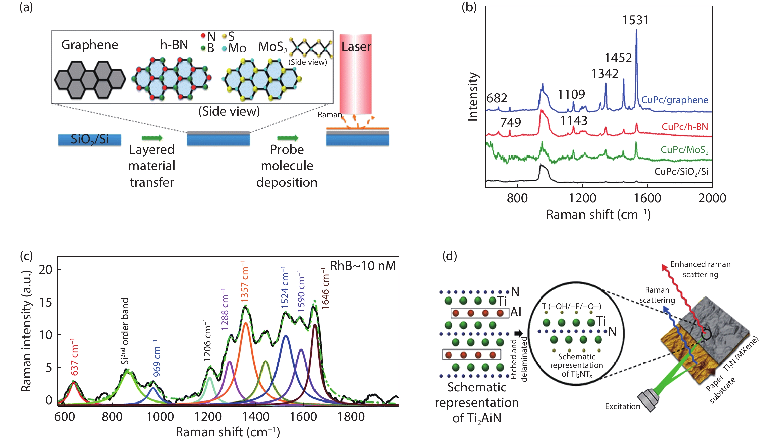
Soundiraraju B, George B K. Two-dimensional titanium nitride (Ti 2N) MXene: Synthesis, characterization, and potential application as surface-enhanced Raman scattering substrate. ACS Nano, 2017, 11, 8892 doi: 10.1021/acsnano.7b03129 |
| [93] |
Ling X, Xie L M, Fang Y, et al. Can graphene be used as a substrate for Raman enhancement. Nano Lett, 2010, 10, 553 doi: 10.1021/nl903414x |
| [94] |
Qiu C Y, Zhou H Q, Yang H C, et al. Investigation of n-layer graphenes as substrates for Raman enhancement of crystal violet. J Phys Chem C, 2011, 115, 10019 doi: 10.1021/jp111617c |
| [95] |
Georgiou T, Jalil R, Belle B D, et al. Vertical field-effect transistor based on graphene-WS 2 heterostructures for flexible and transparent electronics. Nat Nanotechnol, 2013, 8, 100 doi: 10.1038/nnano.2012.224 |
| [96] |
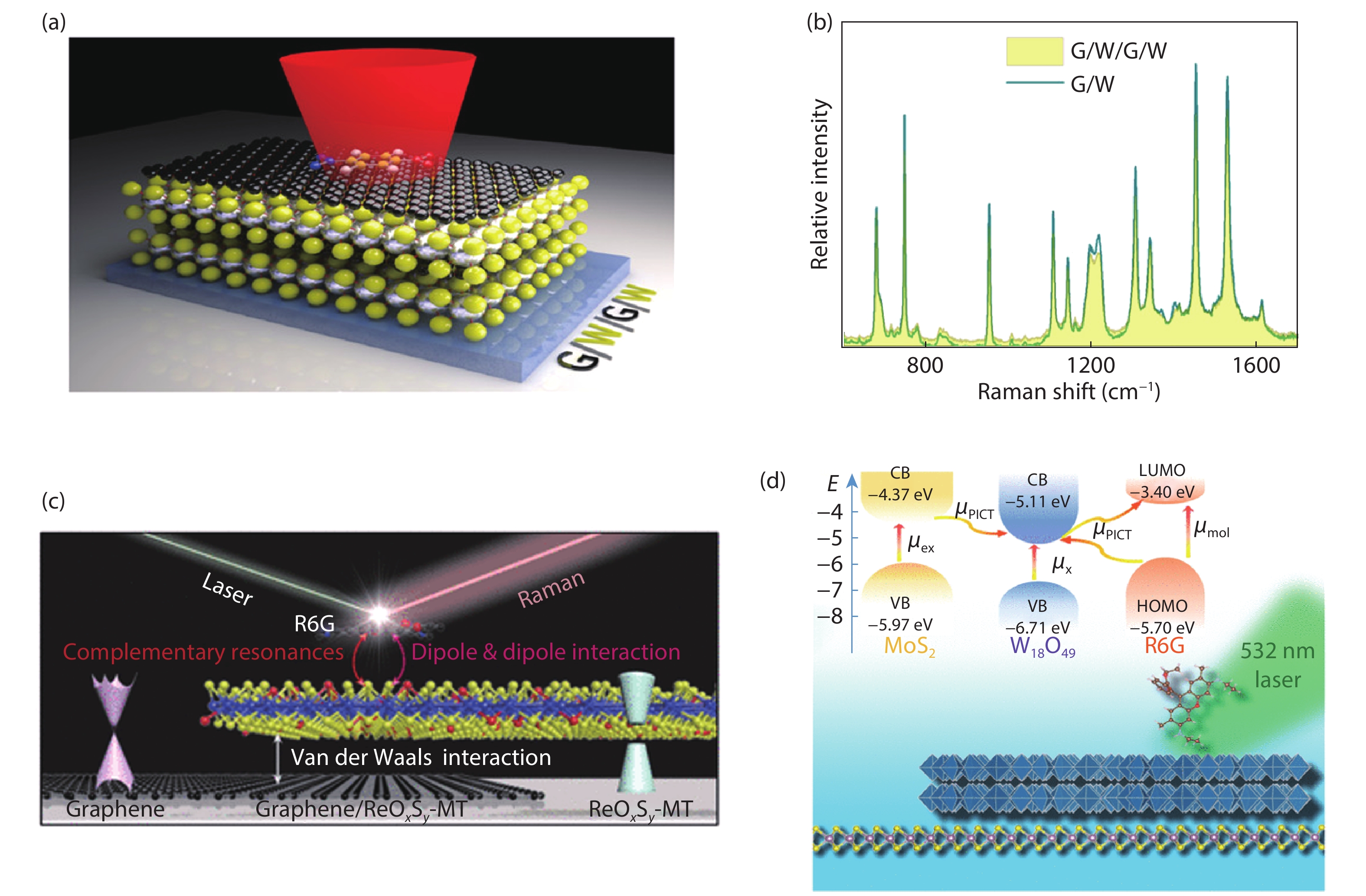
Cai Q R, Gan W, Falin A, et al. Two-dimensional van der waals heterostructures for synergistically improved surface-enhanced Raman spectroscopy. ACS Appl Mater Interfaces, 2020, 12, 21985 doi: 10.1021/acsami.0c01157 |
| [97] |
Yola M L, Atar N. Simultaneous determination of β-agonists on hexagonal boron nitride nanosheets/multi-walled carbon nanotubes nanocomposite modified glassy carbon electrode. Mater Sci Eng C, 2019, 96, 669 doi: 10.1016/j.msec.2018.12.004 |
| [98] |
Ghopry S A, Alamri M A, Goul R, et al. Extraordinary sensitivity of surface-enhanced Raman spectroscopy of molecules on MoS 2 (WS 2) nanodomes/graphene van der Waals heterostructure substrates. Adv Opt Mater, 2019, 7, 1801249 doi: 10.1002/adom.201801249 |
| [99] |
Wu D, Chen J L, Ruan Y E, et al. A novel sensitive and stable surface enhanced Raman scattering substrate based on a MoS 2 quantum dot/reduced graphene oxide hybrid system. J Mater Chem C, 2018, 6, 12547 doi: 10.1039/C8TC05151H |
| [100] |
Qiu H W, Wang M Q, Zhang L, et al. Wrinkled 2H-phase MoS 2 sheet decorated with graphene-microflowers for ultrasensitive molecular sensing by plasmon-free SERS enhancement. Sens Actuator B, 2020, 320, 128445 doi: 10.1016/j.snb.2020.128445 |
| [101] |
Seo J, Lee J, Kim Y, et al. Ultrasensitive plasmon-free surface-enhanced Raman spectroscopy with femtomolar detection limit from 2D van der waals heterostructure. Nano Lett, 2020, 20, 1620 doi: 10.1021/acs.nanolett.9b04645 |
| [102] |
Cong S, Yuan Y, Chen Z, et al. Noble metal-comparable SERS enhancement from semiconducting metal oxides by making oxygen vacancies. Nat Commun, 2015, 6, 7800 doi: 10.1038/ncomms8800 |
| [103] |
Musumeci A, Gosztola D, Schiller T, et al. SERS of semiconducting nanoparticles (TiO 2 hybrid composites). J Am Chem Soc, 2009, 131, 6040 doi: 10.1021/ja808277u |
| [104] |
Li M Z, Fan X C, Gao Y M, et al. W 18O 49/monolayer MoS 2 heterojunction-enhanced Raman scattering. J Phys Chem Lett, 2019, 10, 4038 doi: 10.1021/acs.jpclett.9b00972 |
| [105] |
Xie L M, Ling X, Fang Y, et al. Graphene as a substrate to suppress fluorescence in resonance Raman spectroscopy. J Am Chem Soc, 2009, 131, 9890 doi: 10.1021/ja9037593 |
| [106] |
Xu H, Xie L M, Zhang H L, et al. Effect of graphene fermi level on the Raman scattering intensity of molecules on graphene. ACS Nano, 2011, 5, 5338 doi: 10.1021/nn103237x |
| [107] |
Xu W, Ling X, Xiao J, et al. Surface enhanced Raman spectroscopy on a flat graphene surface. PNAS, 2012, 109, 9281 doi: 10.1073/pnas.1205478109 |
| [108] |
Xu W G, Mao N N, Zhang J. Graphene: A platform for surface-enhanced Raman spectroscopy. Small, 2013, 9, 1206 doi: 10.1002/smll.201203097 |
| [109] |
Kuo C C, Chen C H. Graphene thickness-controlled photocatalysis and surface enhanced Raman scattering. Nanoscale, 2014, 6, 12805 doi: 10.1039/C4NR03877K |
| [110] |
Kim H, Seol M L, Lee D I, et al. Single nanowire on graphene (SNOG) as an efficient, reproducible, and stable SERS-active platform. Nanoscale, 2016, 8, 8878 doi: 10.1039/C6NR00092D |
| [111] |
Huang S X, Pandey R, Barman I, et al. Raman enhancement of blood constituent proteins using graphene. ACS Photonics, 2018, 5, 2978 doi: 10.1021/acsphotonics.8b00456 |
| [112] |
Silver A, Kitadai H, Liu H, et al. Chemical and bio sensing using graphene-enhanced Raman spectroscopy. Nanomaterials, 2019, 9, 516 doi: 10.3390/nano9040516 |
| [113] |
Hou X Y, Zhang X Y, Ma Q W, et al. Alloy engineering in few-layer manganese phosphorus trichalcogenides for surface-enhanced Raman scattering. Adv Funct Mater, 2020, 30, 1910171 doi: 10.1002/adfm.201910171 |
| [114] |
Wang X T, Shi W X, Wang S X, et al. Two-dimensional amorphous TiO 2 nanosheets enabling high-efficiency photoinduced charge transfer for excellent SERS activity. J Am Chem Soc, 2019, 141, 5856 doi: 10.1021/jacs.9b00029 |
| [115] |
Lee M R, Lee H K, Yang Y, et al. Direct metal writing and precise positioning of gold nanoparticles within microfluidic channels for SERS sensing of gaseous analytes. ACS Appl Mater Interfaces, 2017, 9, 39584 doi: 10.1021/acsami.7b11649 |
| [116] |
Oh Y J, Jeong K H. Optofluidic SERS chip with plasmonic nanoprobes self-aligned along microfluidic channels. Lab Chip, 2014, 14, 865 doi: 10.1039/c3lc51257f |
| [117] |
Cheng Z Z, Tsang H K, Wang X M, et al. In-plane optical absorption and free carrier absorption in graphene-on-silicon waveguides. IEEE J Sel Top Quantum Electron, 2014, 20, 43 doi: 10.1109/JSTQE.2013.2263115 |
| [118] |
Wang J Q, Cheng Z Z, Shu C, et al. Optical absorption in graphene-on-silicon nitride microring resonators. IEEE Photonics Technol Lett, 2015, 27, 1765 doi: 10.1109/LPT.2015.2443051 |


 DownLoad: