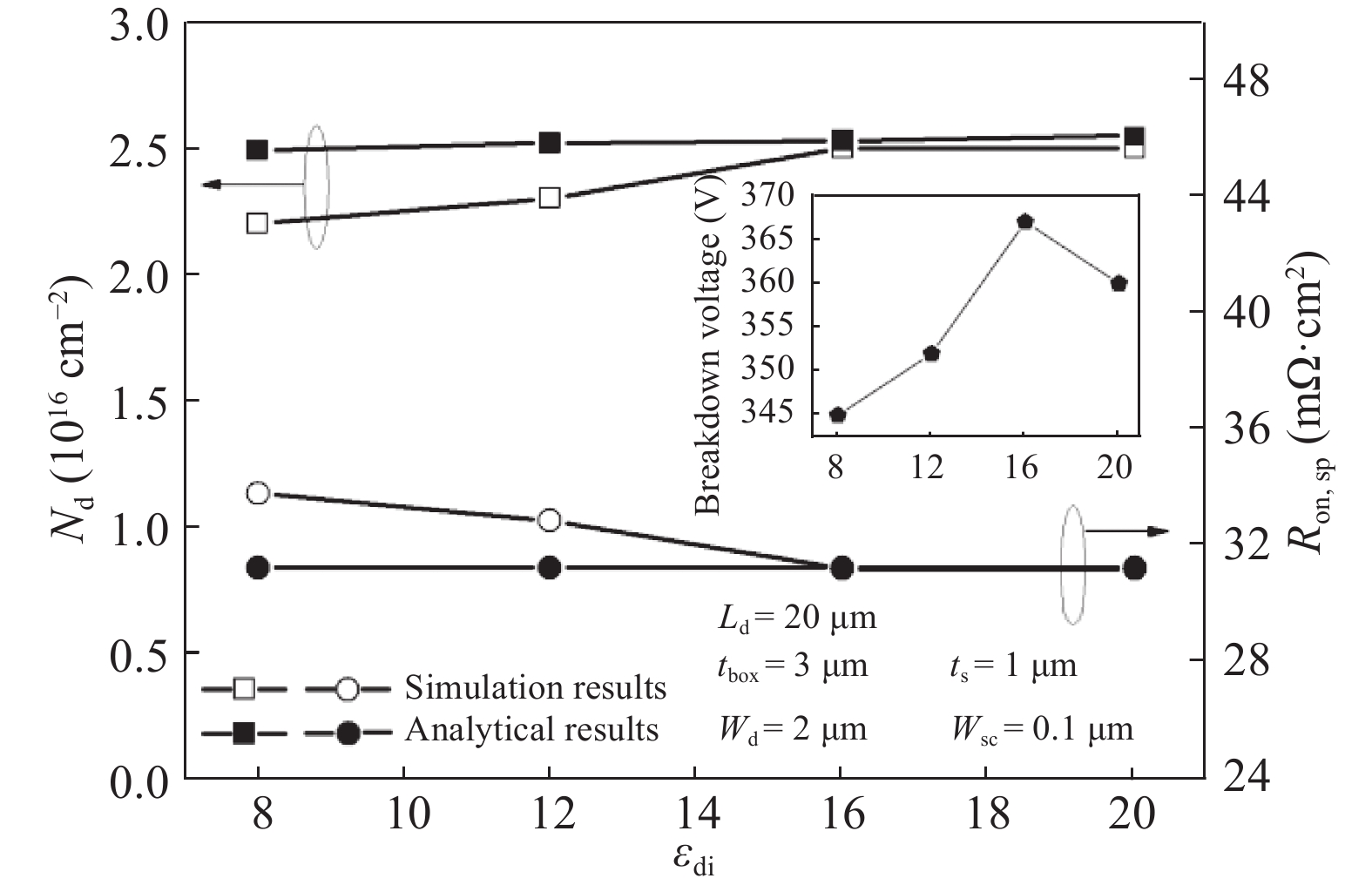
Fig. 1.
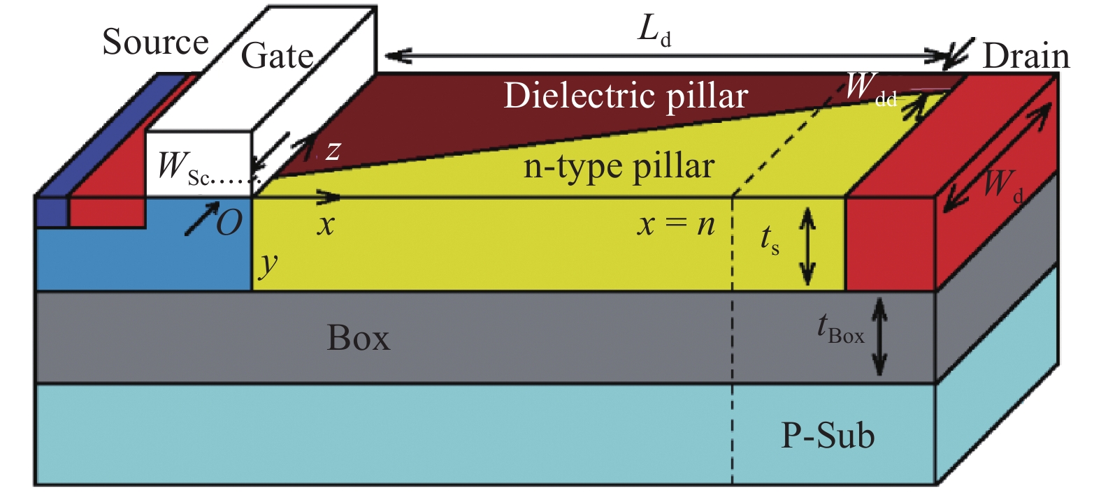
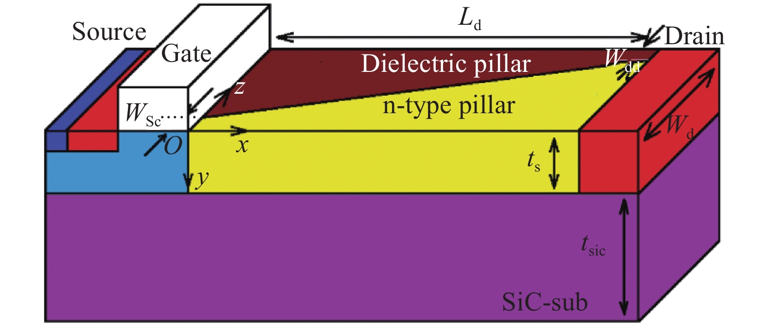
(Color online) Schematic of a half-cell of the VLW SOI LDMOS device.
SEMICONDUCTOR DEVICES
Panpan Tang1, Ying Wang2, , Xiongfei Meng3 and Sufen Cui3
Corresponding author: Ying Wang, Email: wangying7711@yahoo.com
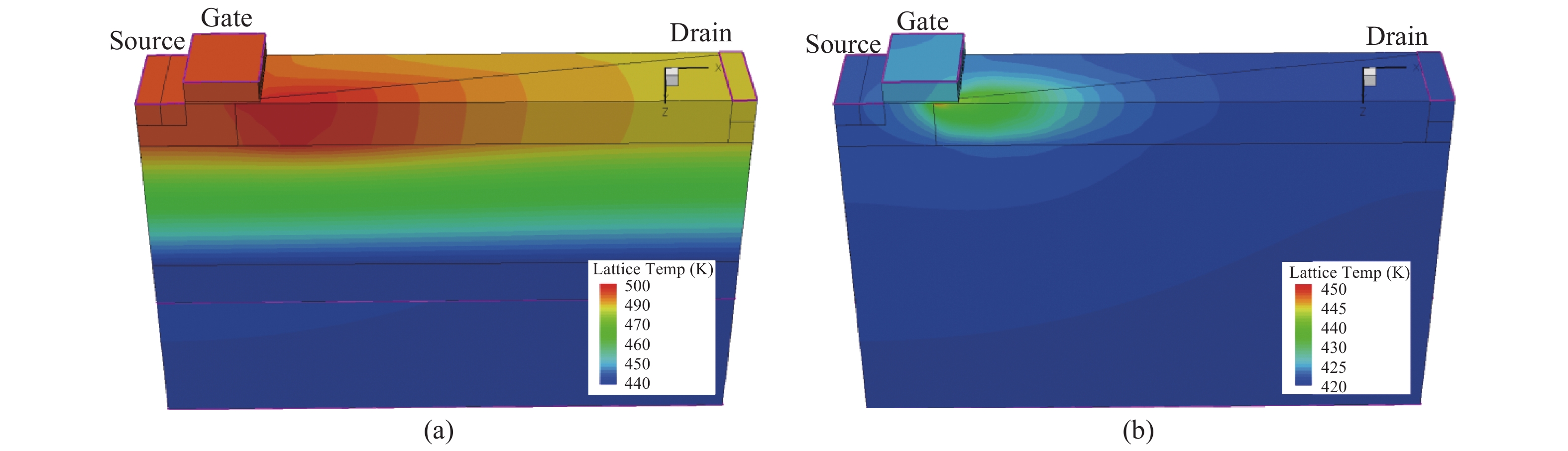
Abstract: The main content revolves round the on-state characteristics of the variation of a lateral width (VLW) LDMOS device. A three-dimensional numerical analysis is performed to investigate the specific on-resistance of the VLW LDMOS device, the simulation results are in good agreement with the analytical calculation results combined with device dimensions. This provides a theoretical basis for the design of devices in the future. Then the self-heating effect of the VLW structure with a silicon-on-oxide (SOI) substrate is compared with that of a silicon carbide (SiC) substrate by 3D thermoelectric simulation. The electrical characteristic and temperature distribution indicate that taking into account the SiC as the substrate can mitigate the self- heating penalty effectively, alleviating the self heating effect and improving reliability.
Key words: SOI, self-heating effect, specific on-resistance, LDMOS transistor
| [1] |
Shimamoto S, Yanagida Y, Shirakawa S, et al. High-performance p-channel LDMOS transistors and wide-range voltage platform technology using novel p-channel structure. IEEE Trans Electron Devices, 2013, 60(1): 360 doi: 10.1109/TED.2012.2228202
|
| [2] |
Hardikar S, Souza M M D, Xu Y Z, et al. A novel double RESURF LDMOS for HVIC's. Microelectron J, 2004, 35(3): 305 doi: 10.1016/S0026-2692(03)00190-3
|
| [3] |
Hu X R, Zhang B, Luo X R, et al. Analytical models for the electric field distributions and breakdown voltage of triple RESURF SOI LDMOS. Solid State Electron, 2012, 69: 89 doi: 10.1016/j.sse.2011.12.010
|
| [4] |
Guo Y F, Yao J F, Zhang B, et al. Variation of lateral width technique in SOI high-voltage lateral double-diffused metal–oxide–semiconductor transistors using high-k dielectric. IEEE Electron Device Lett, 2015, 36(3): 262 doi: 10.1109/LED.2015.2393913
|
| [5] |
Li J H, Li P, Huo W R, et al. Analysis and fabrication of an LDMOS with high-permittivity dielectric. IEEE Electron Device Lett, 2011, 32(9): 1266 doi: 10.1109/LED.2011.2158383
|
| [6] |
Wang Y, Meng X F, Cui S F. Preliminary study and design for variation of lateral width SOI LDMOS device. Solid State Electron, 2016, 116: 65 doi: 10.1016/j.sse.2015.11.039
|
| [7] |
Guo Y, Wang Z, Sheu G, et al. A high performance silicon-on-insulator LDMOSTT using linearly increasing thickness techniques. Chin Phys Lett, 2010, 27(6): 179
|
| [8] |
Zhang S, Sin J K O, Lai T M L, et al. Numerical modeling of linear doping profiles for high-voltage thin-film SOI devices. IEEE Trans Electron Devices, 1999, 46(5): 1036 doi: 10.1109/16.760414
|
| [9] |
Yao J F, Guo Y F, Xia T, et al. 3D analytical model for the SOI LDMOS with alternating silicon and high-k dielectric pillars. Superlattices Microstruct, 2016, 96: 95 doi: 10.1016/j.spmi.2016.05.018
|
| [10] |
Zhang B, Zhang W, Li Z, et al. a novel vertical field plate lateral device with ultralow specific on-resistance. IEEE Trans Electron Devices, 2014, 61(2): 525 doi: 10.1109/TED.2013.2295091
|
| [11] |
Su L T, Chung J E, Antoniadis D A, et al. Measurement and modeling of self-heating effects in SOI nMOSFETs. International Electron Devices Meeting, 1992: 357
|
| [12] |
He P, Liu L, Tian L, et al. Measurement of thermal conductivity of buried oxides of silicon-on-insulator wafers fabricated by separation by implantation of oxygen technology. Appl Phys Lett, 2002, 81(10): 1896 doi: 10.1063/1.1506784
|
| [13] |
Nasri F, Echouchene F, Aissa M F B, et al. Investigation of self-heating effects in a 10-nm SOI-MOSFET with an insulator region using electrothermal modeling. IEEE Trans Electron Devices, 2015, 62(8): 2410 doi: 10.1109/TED.2015.2447212
|
| [14] |
Wang L, Brown A R, Nedjalkov M, et al. impact of self-heating on the statistical variability in bulk and SOI FinFETs. IEEE Trans Electron Devices, 2015, 62(7): 2106 doi: 10.1109/TED.2015.2436351
|
| [15] |
Makovejev S, Raskin J P, Arshad M K M, et al. Impact of self-heating and substrate effects on small-signal output conductance in UTBB SOI MOSFETs. Solid State Electron, 2012, 71(5): 93
|
| [16] |
Leung Y K, Suzuki Y, Goodson K E, et al. Self-heating effect in lateral DMOS on SOI. Proceedings of the 7th International Symposium on Power Semiconductor Devices and ICs, 1995: 136
|
| [17] |
Lun Z, Du G, Qin J, et al. Investigation of self-heating effect in SOI-LDMOS by device simulation. IEEE 11th International Conference on ICSICT, 2012: 1
|
| [18] |
Lim H T, Udrea F, Garner D M, et al. Modelling of self-heating effect in thin SOI and partial SOI LDMOS power devices. Solid State Electron, 1999, 43(7): 1267 doi: 10.1016/S0038-1101(99)00119-7
|
| [19] |
Park J M, Grasser T, Kosina H, et al. A numerical study of partial-SOI LDMOSFETs. Solid State Electron, 2003, 47(2): 275 doi: 10.1016/S0038-1101(02)00207-1
|
| [20] |
Roig J, Flores D, Rebollo J, et al. A 200 V silicon-on-sapphire LDMOS structure with a step oxide extended field plate. Solid State Electron, 2004, 48(2): 245 doi: 10.1016/S0038-1101(03)00314-9
|
| [21] |
Roig J, Flores D, Cortes I, et al. thin film soi and sos ldmos structures with linear doping profile and enlarged field plate. International Conference on Microelectronics, 2004, 1: 141
|
| [22] |
Nassif-Khalil S G, Salama C A T. Super-junction LDMOST on a silicon-on-sapphire substrate. IEEE Trans Electron Devices, 2003, 50(5): 1385 doi: 10.1109/TED.2003.813460
|
| [23] |
Pérez-Tomás A, Jennings M R, Davis M, et al. Characterization and modeling of n–n Si/SiC heterojunction diodes. J Appl Phys, 2007, 102(1): 014505 doi: 10.1063/1.2752148
|
| [24] |
Luo X R, Cai J Y, Fan Y, et al. Novel low-resistance current path UMOS with high-k dielectric pillars. IEEE Trans Electron Devices, 2013, 60(9): 2840 doi: 10.1109/TED.2013.2272086
|
| [25] |
Luo X R, Jiang Y H, Zhou K, et al. Ultralow specific on-resistance superjunction vertical DMOS with high-k dielectric pillar. IEEE Trans Electron Devices, 2012, 33(7): 1042 doi: 10.1109/LED.2012.2196969
|
| [26] |
Chen X, Huang M. A vertical power MOSFET with an interdigitated drift region using high-k insulator. IEEE Trans Electron Devices, 2012, 59(9): 2430 doi: 10.1109/TED.2012.2204890
|
| [27] |
Chen X. Super-junction voltage sustaining layer with alternating semiconductor and high-k dielectric regions. USA Patent, US7230 310, 2007
|
| [28] |
Baliga B J. Fundamentals of power semiconductor devices. New York: Springer, 2008
|
| [29] |
Xie K, Zhao J H, Flemish J R, et al. A high-current and high-temperature 6H-SiC thyristor. IEEE Electron Device Lett, 1996, 17(3): 142 doi: 10.1109/55.485194
|
| [30] |
Kurumi T, Araki R, Kinoshita H, et al. TEM observation of directly bonded interface between Si and SiC. 2012 IEEE International Meeting for Future of Electron Devices, 2012: 1
|
| [31] |
McDaid L J, Hall S, Mellor P H, et al. Physical origin of negative differential resistance in SOI transistors. Electron Lett, 1989, 25(13): 827 doi: 10.1049/el:19890557
|


Article views: 3396 Times PDF downloads: 58 Times Cited by: 0 Times
Received: 06 March 2018 Revised: 08 April 2018 Online: Uncorrected proof: 28 June 2018Published: 01 November 2018
| Citation: |
Panpan Tang, Ying Wang, Xiongfei Meng, Sufen Cui. Investigation of the on-state behaviors of the variation of lateral width LDMOS device by simulation[J]. Journal of Semiconductors, 2018, 39(11): 114007. doi: 10.1088/1674-4926/39/11/114007
P P Tang, Y Wang, X F Meng, S F Cui, Investigation of the on-state behaviors of the variation of lateral width LDMOS device by simulation[J]. J. Semicond., 2018, 39(11): 114007. doi: 10.1088/1674-4926/39/11/114007.
Export: BibTex EndNote

|
| [1] |
Shimamoto S, Yanagida Y, Shirakawa S, et al. High-performance p-channel LDMOS transistors and wide-range voltage platform technology using novel p-channel structure. IEEE Trans Electron Devices, 2013, 60(1): 360 doi: 10.1109/TED.2012.2228202
|
| [2] |
Hardikar S, Souza M M D, Xu Y Z, et al. A novel double RESURF LDMOS for HVIC's. Microelectron J, 2004, 35(3): 305 doi: 10.1016/S0026-2692(03)00190-3
|
| [3] |
Hu X R, Zhang B, Luo X R, et al. Analytical models for the electric field distributions and breakdown voltage of triple RESURF SOI LDMOS. Solid State Electron, 2012, 69: 89 doi: 10.1016/j.sse.2011.12.010
|
| [4] |
Guo Y F, Yao J F, Zhang B, et al. Variation of lateral width technique in SOI high-voltage lateral double-diffused metal–oxide–semiconductor transistors using high-k dielectric. IEEE Electron Device Lett, 2015, 36(3): 262 doi: 10.1109/LED.2015.2393913
|
| [5] |
Li J H, Li P, Huo W R, et al. Analysis and fabrication of an LDMOS with high-permittivity dielectric. IEEE Electron Device Lett, 2011, 32(9): 1266 doi: 10.1109/LED.2011.2158383
|
| [6] |
Wang Y, Meng X F, Cui S F. Preliminary study and design for variation of lateral width SOI LDMOS device. Solid State Electron, 2016, 116: 65 doi: 10.1016/j.sse.2015.11.039
|
| [7] |
Guo Y, Wang Z, Sheu G, et al. A high performance silicon-on-insulator LDMOSTT using linearly increasing thickness techniques. Chin Phys Lett, 2010, 27(6): 179
|
| [8] |
Zhang S, Sin J K O, Lai T M L, et al. Numerical modeling of linear doping profiles for high-voltage thin-film SOI devices. IEEE Trans Electron Devices, 1999, 46(5): 1036 doi: 10.1109/16.760414
|
| [9] |
Yao J F, Guo Y F, Xia T, et al. 3D analytical model for the SOI LDMOS with alternating silicon and high-k dielectric pillars. Superlattices Microstruct, 2016, 96: 95 doi: 10.1016/j.spmi.2016.05.018
|
| [10] |
Zhang B, Zhang W, Li Z, et al. a novel vertical field plate lateral device with ultralow specific on-resistance. IEEE Trans Electron Devices, 2014, 61(2): 525 doi: 10.1109/TED.2013.2295091
|
| [11] |
Su L T, Chung J E, Antoniadis D A, et al. Measurement and modeling of self-heating effects in SOI nMOSFETs. International Electron Devices Meeting, 1992: 357
|
| [12] |
He P, Liu L, Tian L, et al. Measurement of thermal conductivity of buried oxides of silicon-on-insulator wafers fabricated by separation by implantation of oxygen technology. Appl Phys Lett, 2002, 81(10): 1896 doi: 10.1063/1.1506784
|
| [13] |
Nasri F, Echouchene F, Aissa M F B, et al. Investigation of self-heating effects in a 10-nm SOI-MOSFET with an insulator region using electrothermal modeling. IEEE Trans Electron Devices, 2015, 62(8): 2410 doi: 10.1109/TED.2015.2447212
|
| [14] |
Wang L, Brown A R, Nedjalkov M, et al. impact of self-heating on the statistical variability in bulk and SOI FinFETs. IEEE Trans Electron Devices, 2015, 62(7): 2106 doi: 10.1109/TED.2015.2436351
|
| [15] |
Makovejev S, Raskin J P, Arshad M K M, et al. Impact of self-heating and substrate effects on small-signal output conductance in UTBB SOI MOSFETs. Solid State Electron, 2012, 71(5): 93
|
| [16] |
Leung Y K, Suzuki Y, Goodson K E, et al. Self-heating effect in lateral DMOS on SOI. Proceedings of the 7th International Symposium on Power Semiconductor Devices and ICs, 1995: 136
|
| [17] |
Lun Z, Du G, Qin J, et al. Investigation of self-heating effect in SOI-LDMOS by device simulation. IEEE 11th International Conference on ICSICT, 2012: 1
|
| [18] |
Lim H T, Udrea F, Garner D M, et al. Modelling of self-heating effect in thin SOI and partial SOI LDMOS power devices. Solid State Electron, 1999, 43(7): 1267 doi: 10.1016/S0038-1101(99)00119-7
|
| [19] |
Park J M, Grasser T, Kosina H, et al. A numerical study of partial-SOI LDMOSFETs. Solid State Electron, 2003, 47(2): 275 doi: 10.1016/S0038-1101(02)00207-1
|
| [20] |
Roig J, Flores D, Rebollo J, et al. A 200 V silicon-on-sapphire LDMOS structure with a step oxide extended field plate. Solid State Electron, 2004, 48(2): 245 doi: 10.1016/S0038-1101(03)00314-9
|
| [21] |
Roig J, Flores D, Cortes I, et al. thin film soi and sos ldmos structures with linear doping profile and enlarged field plate. International Conference on Microelectronics, 2004, 1: 141
|
| [22] |
Nassif-Khalil S G, Salama C A T. Super-junction LDMOST on a silicon-on-sapphire substrate. IEEE Trans Electron Devices, 2003, 50(5): 1385 doi: 10.1109/TED.2003.813460
|
| [23] |
Pérez-Tomás A, Jennings M R, Davis M, et al. Characterization and modeling of n–n Si/SiC heterojunction diodes. J Appl Phys, 2007, 102(1): 014505 doi: 10.1063/1.2752148
|
| [24] |
Luo X R, Cai J Y, Fan Y, et al. Novel low-resistance current path UMOS with high-k dielectric pillars. IEEE Trans Electron Devices, 2013, 60(9): 2840 doi: 10.1109/TED.2013.2272086
|
| [25] |
Luo X R, Jiang Y H, Zhou K, et al. Ultralow specific on-resistance superjunction vertical DMOS with high-k dielectric pillar. IEEE Trans Electron Devices, 2012, 33(7): 1042 doi: 10.1109/LED.2012.2196969
|
| [26] |
Chen X, Huang M. A vertical power MOSFET with an interdigitated drift region using high-k insulator. IEEE Trans Electron Devices, 2012, 59(9): 2430 doi: 10.1109/TED.2012.2204890
|
| [27] |
Chen X. Super-junction voltage sustaining layer with alternating semiconductor and high-k dielectric regions. USA Patent, US7230 310, 2007
|
| [28] |
Baliga B J. Fundamentals of power semiconductor devices. New York: Springer, 2008
|
| [29] |
Xie K, Zhao J H, Flemish J R, et al. A high-current and high-temperature 6H-SiC thyristor. IEEE Electron Device Lett, 1996, 17(3): 142 doi: 10.1109/55.485194
|
| [30] |
Kurumi T, Araki R, Kinoshita H, et al. TEM observation of directly bonded interface between Si and SiC. 2012 IEEE International Meeting for Future of Electron Devices, 2012: 1
|
| [31] |
McDaid L J, Hall S, Mellor P H, et al. Physical origin of negative differential resistance in SOI transistors. Electron Lett, 1989, 25(13): 827 doi: 10.1049/el:19890557
|

 WeChat ID
Journal of Semiconductors © 2017 All Rights Reserved 京ICP备05085259号-2

 DownLoad: