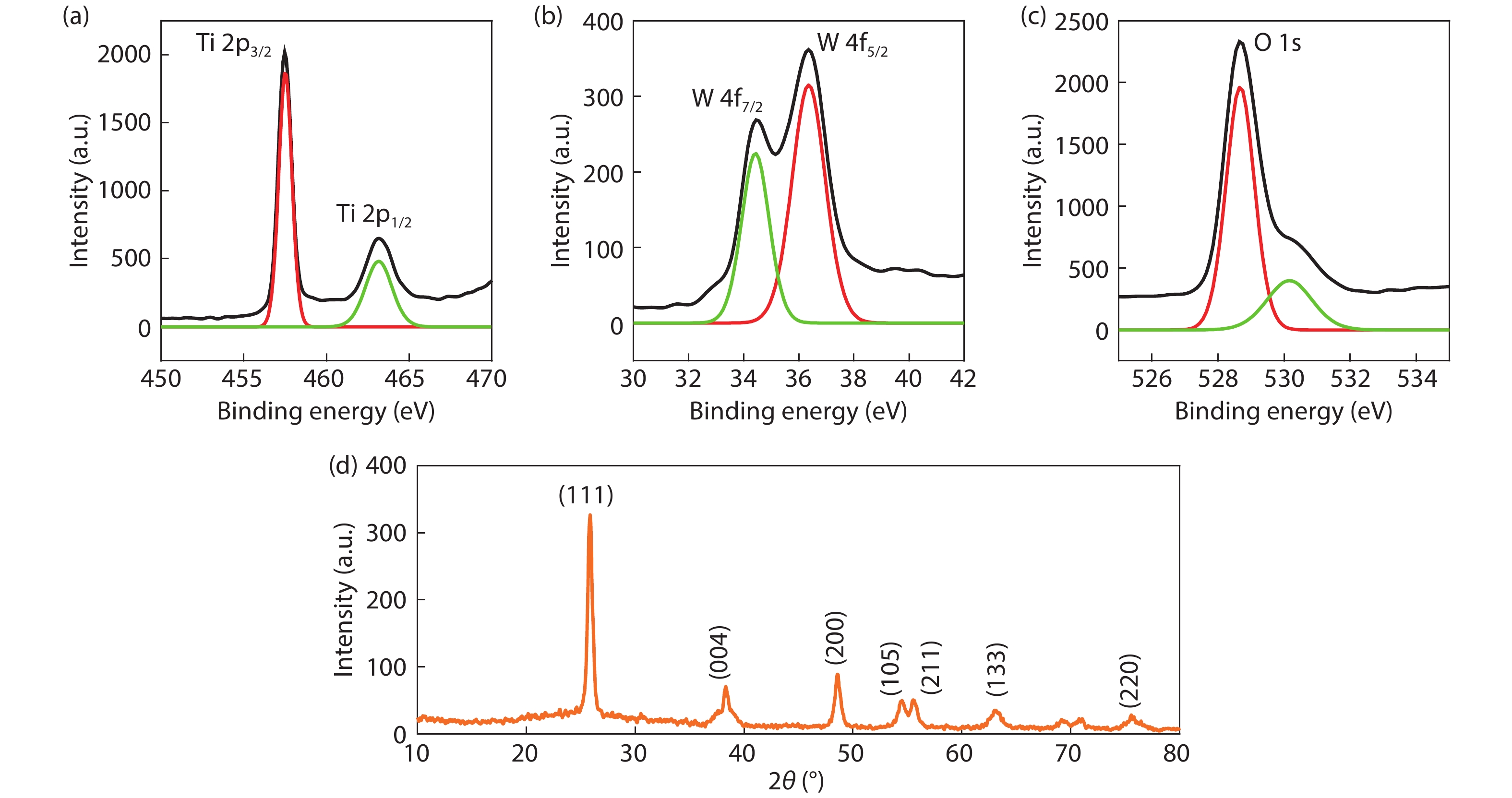
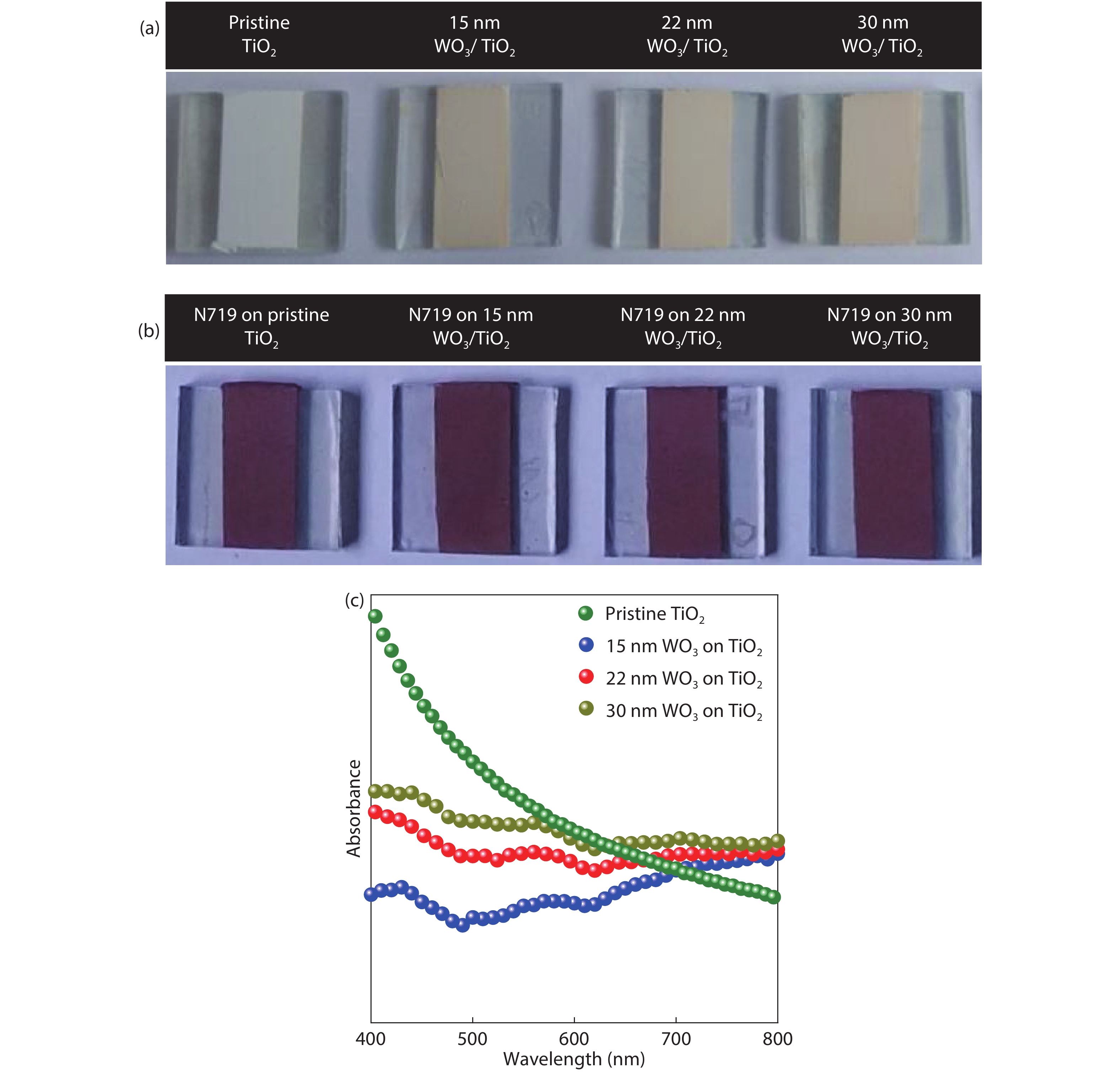
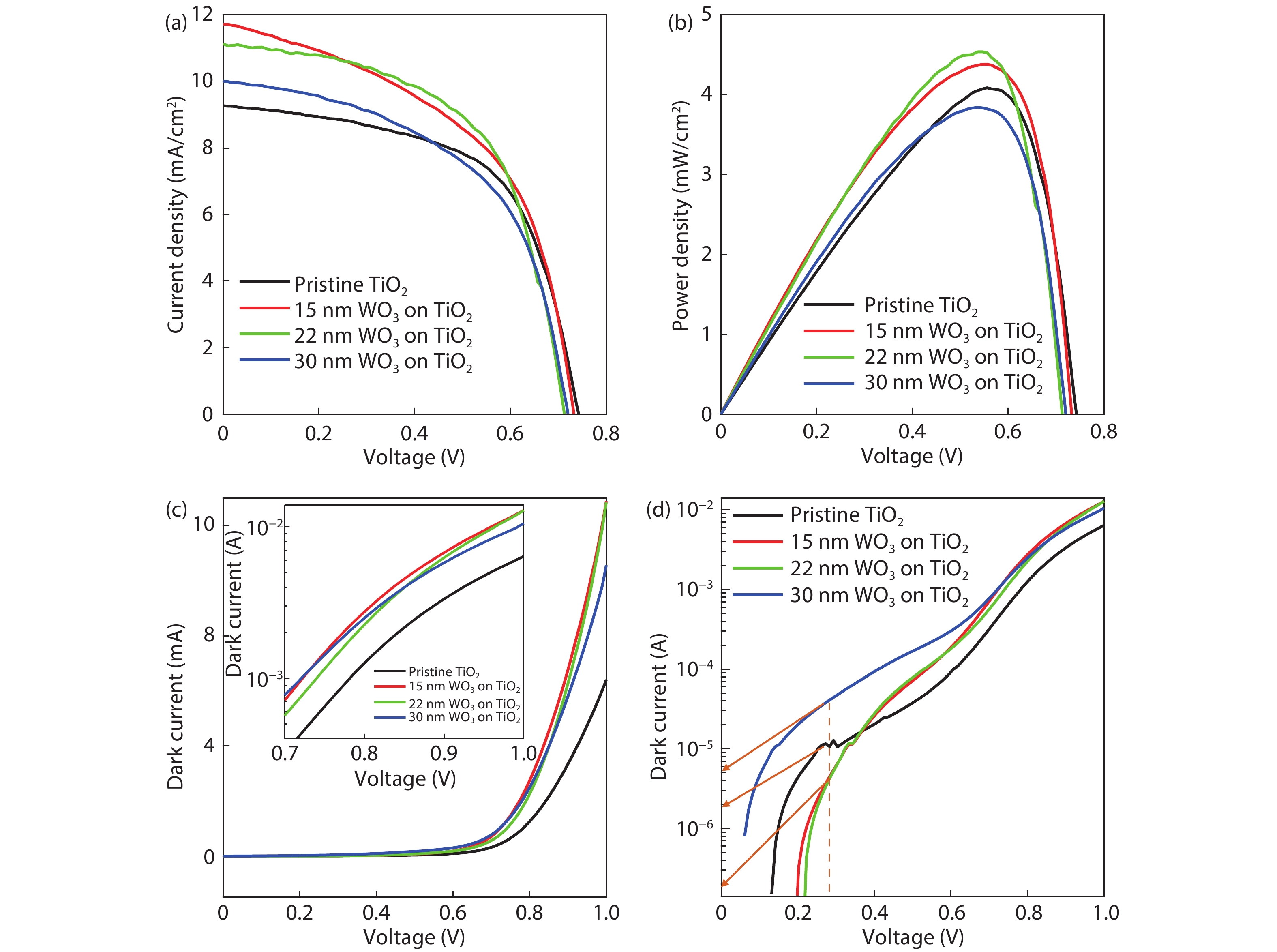
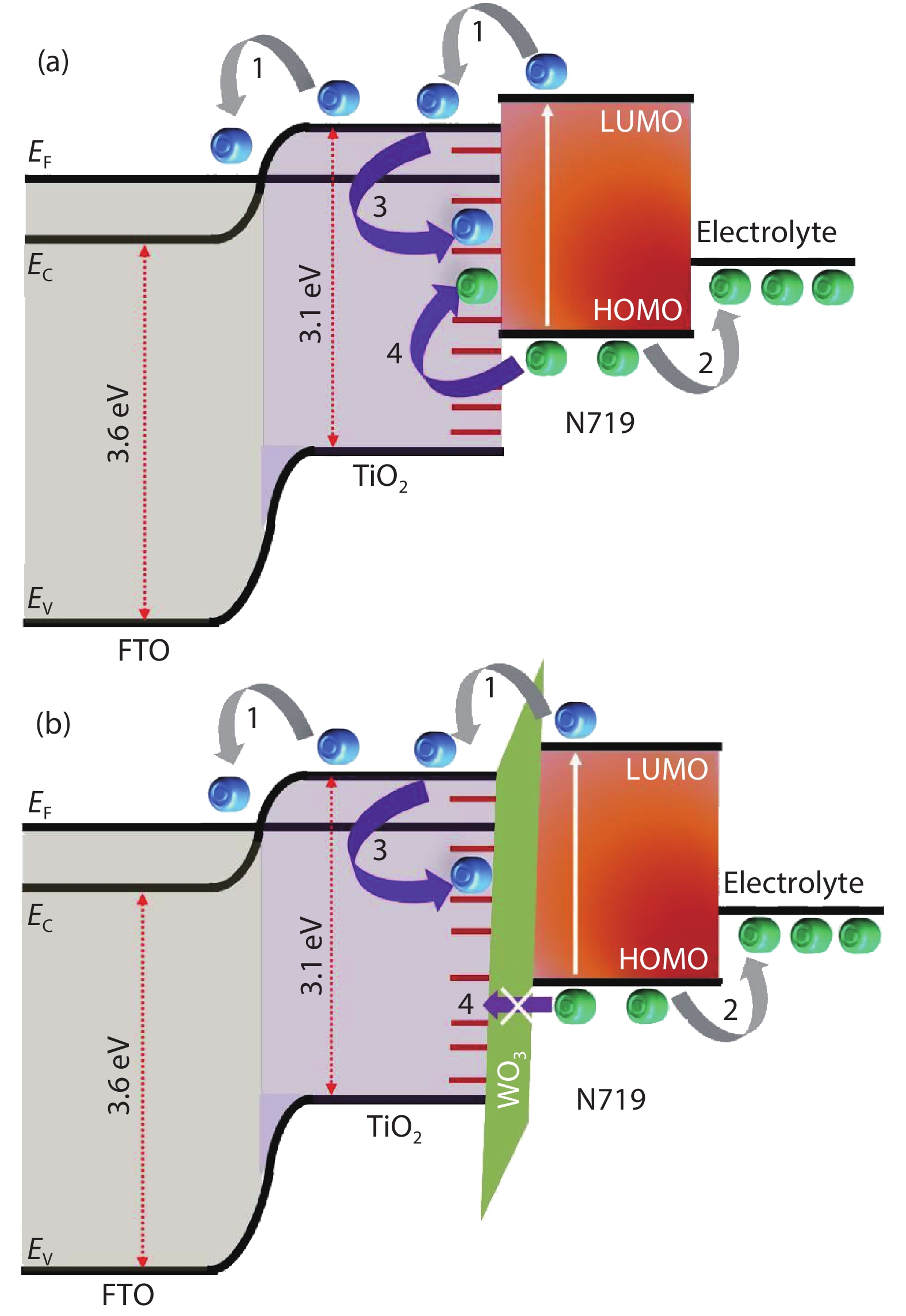
ARTICLES

WO3 passivation layer-coated nanostructured TiO2: An efficient defect engineered photoelectrode for dye sensitized solar cell

Arya Babu, Arya Vasanth, Shantikumar Nair and Mariyappan Shanmugam

+ Author Affiliations

 Corresponding author: Mariyappan Shanmugam, mshanmugham@aims.amrita.edu

PDF

Turn off MathJax

Abstract: Major loss factors for photo-generated electrons due to the presence of surface defects in titanium dioxide (TiO2) were controlled by RF-sputtered tungsten trioxide (WO3) passivation. X-ray photoelectron spectroscopy assured the coating of WO3 on the TiO2 nanoparticle layer by showing Ti 2p, W 4f and O 1s characteristic peaks and were further confirmed by X-ray diffraction studies. The coating of WO3 on the TiO2 nanoparticle layer did not affect dye adsorption significantly. Dye sensitized solar cells (DSSCs) fabricated using WO3-coated TiO2 showed an enhancement of ~10% compared to DSSCs fabricated using pristine TiO2-based photo-electrodes. It is attributed to the WO3 passivation on TiO2 that creates an energy barrier which favored photo-electron injection by tunneling but blocked reverse electron recombination pathways towards holes available in highest occupied molecular orbital of the dye molecules. It was further evidenced that there is an optimum thickness (duration of coating) of WO3 to improve the DSSC performance and longer duration of WO3 suppressed photo-electron injection from dye to TiO2 as inferred from the detrimental effect in short circuit current density values. RF-sputtering yields pinhole-free, highly uniform and conformal coating of WO3 onto any area of interest, which can be considered for an effective surface passivation for nanostructured photovoltaic devices.

Key words: charge transportrecombinationtungsten oxidesolar cellinterfacedefects


[1]
Mlinar V. Engineered nanomaterials for solar energy conversion. Nanotechnology, 2013, 24, 042001 doi: 10.1088/0957-4484/24/4/042001
[2]
Kumar S, Nehra M, Deep A, et al. Quantum-sized nanomaterials for solar cell applications. Renew Sustain Energy Rev, 2017, 73, 821 doi: 10.1016/j.rser.2017.01.172
[3]
Sun H, Deng J, Qiu L B, et al. Recent progress in solar cells based on one-dimensional nanomaterials. Energy Environ Sci, 2015, 8, 1139 doi: 10.1039/C4EE03853C
[4]
Brennan L J, Byrne M T, Bari M, et al. Carbon nanomaterials for dye-sensitized solar cell applications: A bright future. Adv Energy Mater, 2011, 1, 472 doi: 10.1002/aenm.201100136
[5]
Yang N L, Zhai J, Wang D, et al. Two-dimensional graphene bridges enhanced photoinduced charge transport in dye-sensitized solar cells. ACS Nano, 2010, 4, 887 doi: 10.1021/nn901660v
[6]
Yu R, Lin Q F, Leung S F, et al. Nanomaterials and nanostructures for efficient light absorption and photovoltaics. Nano Energy, 2012, 1, 57 doi: 10.1016/j.nanoen.2011.10.002
[7]
Hu Y, Wang H, Hu B. Thinnest two-dimensional nanomaterial— graphene for solar energy. ChemSusChem, 2010, 3, 782 doi: 10.1002/cssc.201000061
[8]
Li W, Elzatahry A, Aldhayan D, et al. Core-shell structured titanium dioxide nanomaterials for solar energy utilization. Chem Soc Rev, 2018, 47, 8203 doi: 10.1039/C8CS00443A
[9]
Su S, Wu W H, Gao J M, et al. Nanomaterials-based sensors for applications in environmental monitoring. J Mater Chem, 2012, 22, 18101 doi: 10.1039/c2jm33284a
[10]
Sun Y M, Liu N, Cui Y. Promises and challenges of nanomaterials for lithium-based rechargeable batteries. Nat Energy, 2016, 1, 16071 doi: 10.1038/nenergy.2016.71
[11]
Gao M, Yao J C, Yan C, et al. Novel composite nanomaterials with superior thermal and pressure stability for potential LED applications. J Alloy Compd, 2018, 734, 282 doi: 10.1016/j.jallcom.2017.11.042
[12]
Ramakrishna G, Singh A K, Palit D K, et al. Dynamics of interfacial electron transfer from photoexcited quinizarin (Qz) into the conduction band of TiO2 and surface states of ZrO2 nanoparticles. J Phys Chem B, 2004, 108, 4775 doi: 10.1021/jp036623r
[13]
Hanzu I, Djenizian T, Knauth P. Electrical and point defect properties of TiO2 nanotubes fabricated by electrochemical anodization. J Phys Chem C, 2011, 115, 5989 doi: 10.1021/jp1111982
[14]
Nasirpouri F, Peighambardoust N S, Samardak A, et al. Structural defect-induced bandgap narrowing in dopant-free anodic TiO2 nanotubes. ChemElectroChem, 2017, 4, 1227 doi: 10.1002/celc.201700038
[15]
Menon H, Gopakumar G, Sankaranarayanan Nair V, et al. 2D-layered MoS2-incorporated TiO2-nanofiber- based dye-sensitized solar cells. ChemistrySelect, 2018, 3, 5801 doi: 10.1002/slct.201702953
[16]
Goban A, Choi K S, Alton D J, et al. Demonstration of a state-insensitive, compensated nanofiber trap. Phys Rev Lett, 2012, 109, 033603 doi: 10.1103/PhysRevLett.109.033603
[17]
Zhu H, Zhao M M, Zhou J K, et al. Surface states as electron transfer pathway enhanced charge separation in TiO2 nanotube water splitting photoanodes. Appl Catal B, 2018, 234, 100 doi: 10.1016/j.apcatb.2018.04.040
[18]
Sachs M, Pastor E, Kafizas A, et al. Evaluation of surface state mediated charge recombination in anatase and rutile TiO2. J Phys Chem Lett, 2016, 7, 3742 doi: 10.1021/acs.jpclett.6b01501
[19]
Zheng J W, Mo L E, Chen W C, et al. An investigation of surface states energy distribution and band edge shifts in solar cells based on TiO2 submicrospheres and nanoparticles. Electrochimica Acta, 2017, 232, 38 doi: 10.1016/j.electacta.2017.02.121
[20]
Sidorova T. A model of electron tunneling to the surface states in TiO2 with application to photocatalysis. Int J Nanosci, 2019, 18, 1940034 doi: 10.1142/S0219581X19400349
[21]
Fàbrega C, Monllor-Satoca D, Ampudia S, et al. Tuning the fermi level and the kinetics of surface states of TiO2 nanorods by means of ammonia treatments. J Phys Chem C, 2013, 117, 20517 doi: 10.1021/jp407167z
[22]
Huber R, Spörlein S, Moser J E, et al. The role of surface states in the ultrafast photoinduced electron transfer from sensitizing dye molecules to semiconductor colloids. J Phys Chem B, 2000, 104, 8995 doi: 10.1021/jp9944381
[23]
Antuch M, Millet P, de Iwase A, et al. The role of surface states during photocurrent switching: Intensity modulated photocurrent spectroscopy analysis of BiVO4 photoelectrodes. Appl Catal B, 2018, 237, 401 doi: 10.1016/j.apcatb.2018.05.011
[24]
Hossain M K, Mortuza A A, Sen S K, et al. A comparative study on the influence of pure anatase and Degussa-P25 TiO2 nanomaterials on the structural and optical properties of dye sensitized solar cell (DSSC) photoanode. Optik, 2018, 171, 507 doi: 10.1016/j.ijleo.2018.05.032
[25]
Kim C K, Ji J M, Zhou H, et al. Tellurium-doped, mesoporous carbon nanomaterials as transparent metal-free counter electrodes for high-performance bifacial dye-sensitized solar cells. Nanomaterials, 2019, 10, E29 doi: 10.3390/nano10010029
[26]
Mehra S, Bishnoi S, Jaiswal A, et al. A review on spectral converting nanomaterials as a photoanode layer in dye-sensitized solar cells with implementation in energy storage devices. Energy Storage, 2020, 2, e120 doi: 10.1002/est2.120
[27]
Tehare K K, Navale S T, Stadler F J, et al. Enhanced DSSCs performance of TiO2 nanostructure by surface passivation layers. Mater Res Bull, 2018, 99, 491 doi: 10.1016/j.materresbull.2017.11.046
[28]
Gopakumar G, Ashok A, Vijayaraghavan S N, et al. MoO3 surface passivation on TiO2: An efficient approach to minimize loss in fill factor and maximum power of dye sensitized solar cell. Appl Surf Sci, 2018, 447, 554 doi: 10.1016/j.apsusc.2018.04.013
[29]
Roelofs K E, Brennan T P, Dominguez J C, et al. Effect of Al2O3 recombination barrier layers deposited by atomic layer deposition in solid-state CdS quantum dot-sensitized solar cells. J Phys Chem C, 2013, 117, 5584 doi: 10.1021/jp311846r
[30]
Pascoe A R, Bourgeois L, Duffy N W, et al. Surface state recombination and passivation in nanocrystalline TiO2 dye-sensitized solar cells. J Phys Chem C, 2013, 117, 25118 doi: 10.1021/jp408055g
[31]
Prasittichai C, Hupp J T. Surface modification of SnO2 photoelectrodes in dye-sensitized solar cells: Significant improvements in photovoltage via Al2O3 atomic layer deposition. J Phys Chem Lett, 2010, 1, 1611 doi: 10.1021/jz100361f
[32]
Palomares E, Clifford J N, Haque S A, et al. Slow charge recombination in dye-sensitised solar cells (DSSC) using Al2O3 coated nanoporous TiO2 films. Chem Commun (Camb), 2002, 14, 1464 doi: 10.1039/b202515a
[33]
Wang Y J, Bai W K, Han S L, et al. Promoted photoelectrocatalytic hydrogen production performance of TiO2 nanowire arrays by Al2O3 surface passivation layer. Curr Catal, 2017, 6, 50 doi: 10.2174/2213337203666161021153243
[34]
Jeong J A, Kim H K. Thickness effect of RF sputtered TiO2 passivating layer on the performance of dye-sensitized solar cells. Sol Energy Mater Sol Cells, 2011, 95, 344 doi: 10.1016/j.solmat.2010.02.008
[35]
Shanmugam M, Jacobs-Gedrim R, Durcan C, et al. 2D layered insulator hexagonal boron nitride enabled surface passivation in dye sensitized solar cells. Nanoscale, 2013, 5, 11275 doi: 10.1039/c3nr03767c
[36]
Yang X J, Zhao L, Lv K, et al. Enhanced efficiency for dye-sensitized solar cells with ZrO2 as a barrier layer on TiO2 nanofibers. Appl Surf Sci, 2019, 469, 821 doi: 10.1016/j.apsusc.2018.10.242
[37]
van Delft J A, Garcia-Alonso D, Kessels W M. Atomic layer deposition for photovoltaics: Applications and prospects for solar cell manufacturing. Semicond Sci Technol, 2012, 27, 074002 doi: 10.1088/0268-1242/27/7/074002
[38]
Vasanth A, Powar N S, Krishnan D, et al. Electrophoretic graphene oxide surface passivation on titanium dioxide for dye sensitized solar cell application. J Sci: Adv Mater Devices, 2020, 5, 316 doi: 10.1016/j.jsamd.2020.07.006
[39]
Flynn C J, McCullough S M, Oh E, et al. Site-selective passivation of defects in NiO solar photocathodes by targeted atomic deposition. ACS Appl Mater Interfaces, 2016, 8, 4754 doi: 10.1021/acsami.6b01090
[40]
Sun H, Kurotaki H, Kanomata K, et al. ZnO/TiO2 core-shell photoelectrodes for dye-sensitized solar cells by screen printing and room temperature ALD. Microsyst Technol, 2018, 24, 647 doi: 10.1007/s00542-017-3389-6
[41]
Bakke J R, Pickrahn K L, Brennan T P, et al. Nanoengineering and interfacial engineering of photovoltaics by atomic layer deposition. Nanoscale, 2011, 3, 3482 doi: 10.1039/c1nr10349k
[42]
Li L P, Chen S K, Xu C, et al. Comparing electron recombination via interfacial modifications in dye-sensitized solar cells. ACS Appl Mater Interfaces, 2014, 6, 20978 doi: 10.1021/am505742y
[43]
Fei C B, Tian J J, Wang Y J, et al. Improved charge generation and collection in dye-sensitized solar cells with modified photoanode surface. Nano Energy, 2014, 10, 353 doi: 10.1016/j.nanoen.2014.10.007
[44]
Kim S A, Abbas M A, Lee L, et al. Control of morphology and defect density in zinc oxide for improved dye-sensitized solar cells. Phys Chem Chem Phys, 2016, 18, 30475 doi: 10.1039/C6CP04204J
[45]
Arthi G, Archana J, Navaneethan M, et al. Hydrothermal growth of ligand-passivated high-surface-area TiO2 nanoparticles and dye-sensitized solar cell characteristics. Scr Mater, 2013, 68, 396 doi: 10.1016/j.scriptamat.2012.10.049
[46]
Rhee S W, Choi H W. Influence of RF magnetron sputtering condition on the ZnO passivating layer for dye-sensitized solar cells. Trans Electr Electron Mater, 2013, 14, 86 doi: 10.4313/TEEM.2013.14.2.86
[47]
Lee S Y, Kim S H. Deposition of TiO2 passivation layer by plasma enhanced chemical vapor deposition between the transparent conducting oxide and mesoporous TiO2 electrode in dye sensitized solar cells. Jpn J Appl Phys, 2012, 51, 10NE19 doi: 10.7567/JJAP.51.10NE19
[48]
Neo C Y, Ouyang J Y. Precise modification of the interface between titanium dioxide and electrolyte of dye-sensitized solar cells with oxides deposited by thermal evaporation of metals and subsequent oxidation. J Power Sources, 2011, 196, 10538 doi: 10.1016/j.jpowsour.2011.08.061
[49]
Jin Y S, Choi H W. Properties of dye-sensitized solar cells with TiO2 passivating layers prepared by electron-beam evaporation. J Nanosci Nanotechnol, 2012, 12, 662 doi: 10.1166/jnn.2012.5408
[50]
Tétreault N, Heiniger L P, Stefik M, et al. Atomic layer deposition for novel dye-sensitized solar cells. ECS Trans, 2019, 41, 303 doi: 10.1149/1.3633681
[51]
Zafar M, Kim B, Kim D H. Improvement in performance of inverted polymer solar cells by interface engineering of ALD ZnS on ZnO electron buffer layer. Appl Surf Sci, 2019, 481, 1442 doi: 10.1016/j.apsusc.2019.03.257
[52]
Cossuet T, Appert E, Chaix-Pluchery O, et al. Epitaxial TiO2 shell grown by atomic layer deposition on ZnO nanowires using a double-step process and its beneficial passivation effect. J Phys Chem C, 2020, 124, 13447 doi: 10.1021/acs.jpcc.0c02605
[53]
Kim D H, Losego M D, Peng Q, et al. Atomic layer deposition for sensitized solar cells: Recent progress and prospects. Adv Mater Interfaces, 2016, 3, 1600354 doi: 10.1002/admi.201600354
[54]
Guerra-Nuñez C, Park H G, Utke I. Atomic layer deposition for surface and interface engineering in nanostructured photovoltaic devices. In: Atomic Layer Deposition in Energy Conversion Applications. Weinheim, Germany: Wiley-VCH Verlag GmbH & Co. KGaA, 2017, 119
[55]
Paula L F, Hofer M, Lacerda V P B, et al. Unraveling the photocatalytic properties of TiO2/WO3 mixed oxides. Photochem Photobiol Sci, 2019, 18, 2469 doi: 10.1039/C9PP00163H
Fig. 1.  Surface morphology of pristine TiO2 at the magnifications of (a) 1000× and (b) 40 000× showing macroscopic clusters and agglomerated particles respectively, (c, d) WO3 coated TiO2 nanoparticles layer showing randomly distributed TiO2 nanoparticles and the porous nature.

Fig. 2.  (Color online) (a–c) High resolution XPS scans showing Ti 2p, W 4f and O 1s peaks from the WO3 coated TiO2 sample. (d) XRD pattern obtained from the same sample.

Fig. 3.  (Color online) Digital photographic images of (a) TiO2 nanoparticle layer coated on FTO covered glass substrates showing the deposition of WO3 surface passivation layer with different thickness values. (b) Photographs of the samples after N719 dye coating confirming the WO3 did not affect the loading much. (c) UV–visible absorption spectra of the samples.

Fig. 4.  (Color online) (a) JV characteristics of the DSSC with and without WO3 passivation on TiO2. (b) Comparison of PMAX of DSSCs, dark current characteristics of DSSCs in (c) linear and (d)semi-log scale showing the saturation current values.

Fig. 5.  (Color online) Schematic illustration of (a) FTO/TiO2/dye/electrolyte and (b) FTO/TiO2/WO3/Dye/electrolyte interfaces in DSSCs showing electron–hole transport and recombination mediated by defects in TiO2.

Table 1.   Photovoltaic parameters of the DSSCs measured under AM1.5 illumination level.

DSSCsWO3 coating duration (min)VOC (mV)JSC (mA/
cm2)
FF (%)η (%)SD in η
Pristine TiO274509.359.04.10.05
15 nm WO3 on TiO2773211.850.84.30.06
22 nm WO3 on TiO21071211.157.24.50.10
30 nm WO3 on TiO21572010.053.13.80.09
DownLoad: CSV
[1]
Mlinar V. Engineered nanomaterials for solar energy conversion. Nanotechnology, 2013, 24, 042001 doi: 10.1088/0957-4484/24/4/042001
[2]
Kumar S, Nehra M, Deep A, et al. Quantum-sized nanomaterials for solar cell applications. Renew Sustain Energy Rev, 2017, 73, 821 doi: 10.1016/j.rser.2017.01.172
[3]
Sun H, Deng J, Qiu L B, et al. Recent progress in solar cells based on one-dimensional nanomaterials. Energy Environ Sci, 2015, 8, 1139 doi: 10.1039/C4EE03853C
[4]
Brennan L J, Byrne M T, Bari M, et al. Carbon nanomaterials for dye-sensitized solar cell applications: A bright future. Adv Energy Mater, 2011, 1, 472 doi: 10.1002/aenm.201100136
[5]
Yang N L, Zhai J, Wang D, et al. Two-dimensional graphene bridges enhanced photoinduced charge transport in dye-sensitized solar cells. ACS Nano, 2010, 4, 887 doi: 10.1021/nn901660v
[6]
Yu R, Lin Q F, Leung S F, et al. Nanomaterials and nanostructures for efficient light absorption and photovoltaics. Nano Energy, 2012, 1, 57 doi: 10.1016/j.nanoen.2011.10.002
[7]
Hu Y, Wang H, Hu B. Thinnest two-dimensional nanomaterial— graphene for solar energy. ChemSusChem, 2010, 3, 782 doi: 10.1002/cssc.201000061
[8]
Li W, Elzatahry A, Aldhayan D, et al. Core-shell structured titanium dioxide nanomaterials for solar energy utilization. Chem Soc Rev, 2018, 47, 8203 doi: 10.1039/C8CS00443A
[9]
Su S, Wu W H, Gao J M, et al. Nanomaterials-based sensors for applications in environmental monitoring. J Mater Chem, 2012, 22, 18101 doi: 10.1039/c2jm33284a
[10]
Sun Y M, Liu N, Cui Y. Promises and challenges of nanomaterials for lithium-based rechargeable batteries. Nat Energy, 2016, 1, 16071 doi: 10.1038/nenergy.2016.71
[11]
Gao M, Yao J C, Yan C, et al. Novel composite nanomaterials with superior thermal and pressure stability for potential LED applications. J Alloy Compd, 2018, 734, 282 doi: 10.1016/j.jallcom.2017.11.042
[12]
Ramakrishna G, Singh A K, Palit D K, et al. Dynamics of interfacial electron transfer from photoexcited quinizarin (Qz) into the conduction band of TiO2 and surface states of ZrO2 nanoparticles. J Phys Chem B, 2004, 108, 4775 doi: 10.1021/jp036623r
[13]
Hanzu I, Djenizian T, Knauth P. Electrical and point defect properties of TiO2 nanotubes fabricated by electrochemical anodization. J Phys Chem C, 2011, 115, 5989 doi: 10.1021/jp1111982
[14]
Nasirpouri F, Peighambardoust N S, Samardak A, et al. Structural defect-induced bandgap narrowing in dopant-free anodic TiO2 nanotubes. ChemElectroChem, 2017, 4, 1227 doi: 10.1002/celc.201700038
[15]
Menon H, Gopakumar G, Sankaranarayanan Nair V, et al. 2D-layered MoS2-incorporated TiO2-nanofiber- based dye-sensitized solar cells. ChemistrySelect, 2018, 3, 5801 doi: 10.1002/slct.201702953
[16]
Goban A, Choi K S, Alton D J, et al. Demonstration of a state-insensitive, compensated nanofiber trap. Phys Rev Lett, 2012, 109, 033603 doi: 10.1103/PhysRevLett.109.033603
[17]
Zhu H, Zhao M M, Zhou J K, et al. Surface states as electron transfer pathway enhanced charge separation in TiO2 nanotube water splitting photoanodes. Appl Catal B, 2018, 234, 100 doi: 10.1016/j.apcatb.2018.04.040
[18]
Sachs M, Pastor E, Kafizas A, et al. Evaluation of surface state mediated charge recombination in anatase and rutile TiO2. J Phys Chem Lett, 2016, 7, 3742 doi: 10.1021/acs.jpclett.6b01501
[19]
Zheng J W, Mo L E, Chen W C, et al. An investigation of surface states energy distribution and band edge shifts in solar cells based on TiO2 submicrospheres and nanoparticles. Electrochimica Acta, 2017, 232, 38 doi: 10.1016/j.electacta.2017.02.121
[20]
Sidorova T. A model of electron tunneling to the surface states in TiO2 with application to photocatalysis. Int J Nanosci, 2019, 18, 1940034 doi: 10.1142/S0219581X19400349
[21]
Fàbrega C, Monllor-Satoca D, Ampudia S, et al. Tuning the fermi level and the kinetics of surface states of TiO2 nanorods by means of ammonia treatments. J Phys Chem C, 2013, 117, 20517 doi: 10.1021/jp407167z
[22]
Huber R, Spörlein S, Moser J E, et al. The role of surface states in the ultrafast photoinduced electron transfer from sensitizing dye molecules to semiconductor colloids. J Phys Chem B, 2000, 104, 8995 doi: 10.1021/jp9944381
[23]
Antuch M, Millet P, de Iwase A, et al. The role of surface states during photocurrent switching: Intensity modulated photocurrent spectroscopy analysis of BiVO4 photoelectrodes. Appl Catal B, 2018, 237, 401 doi: 10.1016/j.apcatb.2018.05.011
[24]
Hossain M K, Mortuza A A, Sen S K, et al. A comparative study on the influence of pure anatase and Degussa-P25 TiO2 nanomaterials on the structural and optical properties of dye sensitized solar cell (DSSC) photoanode. Optik, 2018, 171, 507 doi: 10.1016/j.ijleo.2018.05.032
[25]
Kim C K, Ji J M, Zhou H, et al. Tellurium-doped, mesoporous carbon nanomaterials as transparent metal-free counter electrodes for high-performance bifacial dye-sensitized solar cells. Nanomaterials, 2019, 10, E29 doi: 10.3390/nano10010029
[26]
Mehra S, Bishnoi S, Jaiswal A, et al. A review on spectral converting nanomaterials as a photoanode layer in dye-sensitized solar cells with implementation in energy storage devices. Energy Storage, 2020, 2, e120 doi: 10.1002/est2.120
[27]
Tehare K K, Navale S T, Stadler F J, et al. Enhanced DSSCs performance of TiO2 nanostructure by surface passivation layers. Mater Res Bull, 2018, 99, 491 doi: 10.1016/j.materresbull.2017.11.046
[28]
Gopakumar G, Ashok A, Vijayaraghavan S N, et al. MoO3 surface passivation on TiO2: An efficient approach to minimize loss in fill factor and maximum power of dye sensitized solar cell. Appl Surf Sci, 2018, 447, 554 doi: 10.1016/j.apsusc.2018.04.013
[29]
Roelofs K E, Brennan T P, Dominguez J C, et al. Effect of Al2O3 recombination barrier layers deposited by atomic layer deposition in solid-state CdS quantum dot-sensitized solar cells. J Phys Chem C, 2013, 117, 5584 doi: 10.1021/jp311846r
[30]
Pascoe A R, Bourgeois L, Duffy N W, et al. Surface state recombination and passivation in nanocrystalline TiO2 dye-sensitized solar cells. J Phys Chem C, 2013, 117, 25118 doi: 10.1021/jp408055g
[31]
Prasittichai C, Hupp J T. Surface modification of SnO2 photoelectrodes in dye-sensitized solar cells: Significant improvements in photovoltage via Al2O3 atomic layer deposition. J Phys Chem Lett, 2010, 1, 1611 doi: 10.1021/jz100361f
[32]
Palomares E, Clifford J N, Haque S A, et al. Slow charge recombination in dye-sensitised solar cells (DSSC) using Al2O3 coated nanoporous TiO2 films. Chem Commun (Camb), 2002, 14, 1464 doi: 10.1039/b202515a
[33]
Wang Y J, Bai W K, Han S L, et al. Promoted photoelectrocatalytic hydrogen production performance of TiO2 nanowire arrays by Al2O3 surface passivation layer. Curr Catal, 2017, 6, 50 doi: 10.2174/2213337203666161021153243
[34]
Jeong J A, Kim H K. Thickness effect of RF sputtered TiO2 passivating layer on the performance of dye-sensitized solar cells. Sol Energy Mater Sol Cells, 2011, 95, 344 doi: 10.1016/j.solmat.2010.02.008
[35]
Shanmugam M, Jacobs-Gedrim R, Durcan C, et al. 2D layered insulator hexagonal boron nitride enabled surface passivation in dye sensitized solar cells. Nanoscale, 2013, 5, 11275 doi: 10.1039/c3nr03767c
[36]
Yang X J, Zhao L, Lv K, et al. Enhanced efficiency for dye-sensitized solar cells with ZrO2 as a barrier layer on TiO2 nanofibers. Appl Surf Sci, 2019, 469, 821 doi: 10.1016/j.apsusc.2018.10.242
[37]
van Delft J A, Garcia-Alonso D, Kessels W M. Atomic layer deposition for photovoltaics: Applications and prospects for solar cell manufacturing. Semicond Sci Technol, 2012, 27, 074002 doi: 10.1088/0268-1242/27/7/074002
[38]
Vasanth A, Powar N S, Krishnan D, et al. Electrophoretic graphene oxide surface passivation on titanium dioxide for dye sensitized solar cell application. J Sci: Adv Mater Devices, 2020, 5, 316 doi: 10.1016/j.jsamd.2020.07.006
[39]
Flynn C J, McCullough S M, Oh E, et al. Site-selective passivation of defects in NiO solar photocathodes by targeted atomic deposition. ACS Appl Mater Interfaces, 2016, 8, 4754 doi: 10.1021/acsami.6b01090
[40]
Sun H, Kurotaki H, Kanomata K, et al. ZnO/TiO2 core-shell photoelectrodes for dye-sensitized solar cells by screen printing and room temperature ALD. Microsyst Technol, 2018, 24, 647 doi: 10.1007/s00542-017-3389-6
[41]
Bakke J R, Pickrahn K L, Brennan T P, et al. Nanoengineering and interfacial engineering of photovoltaics by atomic layer deposition. Nanoscale, 2011, 3, 3482 doi: 10.1039/c1nr10349k
[42]
Li L P, Chen S K, Xu C, et al. Comparing electron recombination via interfacial modifications in dye-sensitized solar cells. ACS Appl Mater Interfaces, 2014, 6, 20978 doi: 10.1021/am505742y
[43]
Fei C B, Tian J J, Wang Y J, et al. Improved charge generation and collection in dye-sensitized solar cells with modified photoanode surface. Nano Energy, 2014, 10, 353 doi: 10.1016/j.nanoen.2014.10.007
[44]
Kim S A, Abbas M A, Lee L, et al. Control of morphology and defect density in zinc oxide for improved dye-sensitized solar cells. Phys Chem Chem Phys, 2016, 18, 30475 doi: 10.1039/C6CP04204J
[45]
Arthi G, Archana J, Navaneethan M, et al. Hydrothermal growth of ligand-passivated high-surface-area TiO2 nanoparticles and dye-sensitized solar cell characteristics. Scr Mater, 2013, 68, 396 doi: 10.1016/j.scriptamat.2012.10.049
[46]
Rhee S W, Choi H W. Influence of RF magnetron sputtering condition on the ZnO passivating layer for dye-sensitized solar cells. Trans Electr Electron Mater, 2013, 14, 86 doi: 10.4313/TEEM.2013.14.2.86
[47]
Lee S Y, Kim S H. Deposition of TiO2 passivation layer by plasma enhanced chemical vapor deposition between the transparent conducting oxide and mesoporous TiO2 electrode in dye sensitized solar cells. Jpn J Appl Phys, 2012, 51, 10NE19 doi: 10.7567/JJAP.51.10NE19
[48]
Neo C Y, Ouyang J Y. Precise modification of the interface between titanium dioxide and electrolyte of dye-sensitized solar cells with oxides deposited by thermal evaporation of metals and subsequent oxidation. J Power Sources, 2011, 196, 10538 doi: 10.1016/j.jpowsour.2011.08.061
[49]
Jin Y S, Choi H W. Properties of dye-sensitized solar cells with TiO2 passivating layers prepared by electron-beam evaporation. J Nanosci Nanotechnol, 2012, 12, 662 doi: 10.1166/jnn.2012.5408
[50]
Tétreault N, Heiniger L P, Stefik M, et al. Atomic layer deposition for novel dye-sensitized solar cells. ECS Trans, 2019, 41, 303 doi: 10.1149/1.3633681
[51]
Zafar M, Kim B, Kim D H. Improvement in performance of inverted polymer solar cells by interface engineering of ALD ZnS on ZnO electron buffer layer. Appl Surf Sci, 2019, 481, 1442 doi: 10.1016/j.apsusc.2019.03.257
[52]
Cossuet T, Appert E, Chaix-Pluchery O, et al. Epitaxial TiO2 shell grown by atomic layer deposition on ZnO nanowires using a double-step process and its beneficial passivation effect. J Phys Chem C, 2020, 124, 13447 doi: 10.1021/acs.jpcc.0c02605
[53]
Kim D H, Losego M D, Peng Q, et al. Atomic layer deposition for sensitized solar cells: Recent progress and prospects. Adv Mater Interfaces, 2016, 3, 1600354 doi: 10.1002/admi.201600354
[54]
Guerra-Nuñez C, Park H G, Utke I. Atomic layer deposition for surface and interface engineering in nanostructured photovoltaic devices. In: Atomic Layer Deposition in Energy Conversion Applications. Weinheim, Germany: Wiley-VCH Verlag GmbH & Co. KGaA, 2017, 119
[55]
Paula L F, Hofer M, Lacerda V P B, et al. Unraveling the photocatalytic properties of TiO2/WO3 mixed oxides. Photochem Photobiol Sci, 2019, 18, 2469 doi: 10.1039/C9PP00163H
  • Search

    Advanced Search >>

    GET CITATION

    shu

    Export: BibTex EndNote

    Article Metrics

    Article views: 2788 Times PDF downloads: 55 Times Cited by: 0 Times

    History

    Received: 20 August 2020 Revised: 01 December 2020 Online: Accepted Manuscript: 03 February 2021Uncorrected proof: 23 February 2021Published: 01 May 2021

    Catalog

      Email This Article

      User name:
      Email:*请输入正确邮箱
      Code:*验证码错误
      Arya Babu, Arya Vasanth, Shantikumar Nair, Mariyappan Shanmugam. WO3 passivation layer-coated nanostructured TiO2: An efficient defect engineered photoelectrode for dye sensitized solar cell[J]. Journal of Semiconductors, 2021, 42(5): 052701. doi: 10.1088/1674-4926/42/5/052701 A Babu, A Vasanth, S Nair, M Shanmugam, WO3 passivation layer-coated nanostructured TiO2: An efficient defect engineered photoelectrode for dye sensitized solar cell[J]. J. Semicond., 2021, 42(5): 052701. doi: 10.1088/1674-4926/42/5/052701.Export: BibTex EndNote
      Citation:
      Arya Babu, Arya Vasanth, Shantikumar Nair, Mariyappan Shanmugam. WO3 passivation layer-coated nanostructured TiO2: An efficient defect engineered photoelectrode for dye sensitized solar cell[J]. Journal of Semiconductors, 2021, 42(5): 052701. doi: 10.1088/1674-4926/42/5/052701

      A Babu, A Vasanth, S Nair, M Shanmugam, WO3 passivation layer-coated nanostructured TiO2: An efficient defect engineered photoelectrode for dye sensitized solar cell[J]. J. Semicond., 2021, 42(5): 052701. doi: 10.1088/1674-4926/42/5/052701.
      Export: BibTex EndNote

      WO3 passivation layer-coated nanostructured TiO2: An efficient defect engineered photoelectrode for dye sensitized solar cell

      doi: 10.1088/1674-4926/42/5/052701
      More Information
      • Author Bio:

        Arya Babu received her Master degree in Nanoscience and Nanotechnology in 2020 from Amrita Centre for Nanosciences and Molecular Medicine, Kochi, India. Her major research is focusing on the development of semiconductor nanostructures for energy conversion applications

        Mariyappan Shanmugam received PhD degree from South Dakota State University, USA, in 2011. He is currently working at Amrita Centre for Nanosciences and Molecular Medicine, Kochi, India. He carried out his postdoctoral research at the College of Nanoscale Science and Engineering, State University of New York and Worcester Polytechnic Institute during 2011–2015. His major research is on the development of semiconductor nanostructures and 2D-layered materials for Optoelectronics

      • Corresponding author: mshanmugham@aims.amrita.edu
      • Received Date: 2020-08-20
      • Revised Date: 2020-12-01
      • Published Date: 2021-05-10

      Catalog

        /

        DownLoad:  Full-Size Img  PowerPoint
        Return
        Return