


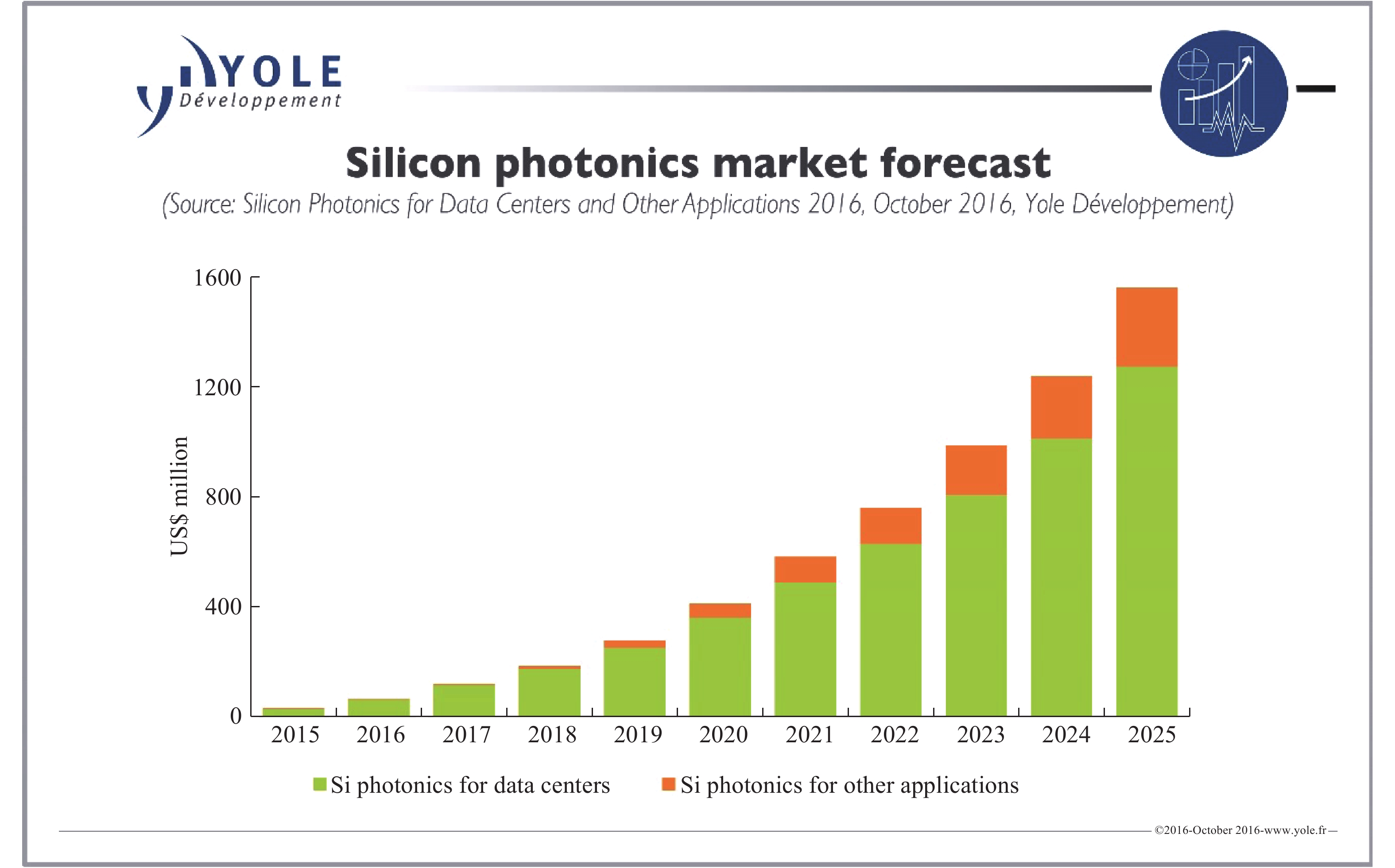
Fig. 1.
(Color online) Silicon photonics 2015–2025 market forecast. Reprinted from Ref. [8]. Silicon Photonics Report with permission from Yole Développement. © Yole Développement 2016.
SPECIAL ISSUE ON Si-BASED MATERIALS AND DEVICES
Corresponding author: Xiaoxin Wang, Wang@Dartmouth.Edu; Jifeng Liu, Jifeng.Liu@Dartmouth.Edu
Abstract: Silicon photonics for synergistic electronic–photonic integration has achieved remarkable progress in the past two decades. Active photonic devices, including lasers, modulators, and photodetectors, are the key challenges for Si photonics to meet the requirement of high bandwidth and low power consumption in photonic datalinks. Here we review recent efforts and progress in high-performance active photonic devices on Si, focusing on emerging technologies beyond conventional foundry-ready Si photonics devices. For emerging laser sources, we will discuss recent progress towards efficient monolithic Ge lasers, mid-infrared GeSn lasers, and high-performance InAs quantum dot lasers on Si for data center applications in the near future. We will then review novel modulator materials and devices beyond the free carrier plasma dispersion effect in Si, including GeSi and graphene electro-absorption modulators and plasmonic-organic electro-optical modulators, to achieve ultralow power and high speed modulation. Finally, we discuss emerging photodetectors beyond epitaxial Ge p–i–n photodiodes, including GeSn mid-infrared photodetectors, all-Si plasmonic Schottky infrared photodetectors, and Si quanta image sensors for non-avalanche, low noise single photon detection and photon counting. These emerging technologies, though still under development, could make a significant impact on the future of large-scale electronicSilicon photonics for synergistic electronic-photonic integration has achieved remarkable progress in the past two decades. Active photonic devices, including lasers, modulators, and photodetectors, are the key challenges for Si photonics to meet the requirement of high bandwidth and low power consumption in photonic datalinks. Here we review recent efforts and progress in high-performance active photonic devices on Si, focusing on emerging technologies beyond conventional foundry-ready Si photonics devices. For emerging laser sources, we will discuss recent progress towards efficient monolithic Ge lasers, mid-infrared GeSn lasers, and high-performance InAs quantum dot lasers on Si for data center applications in the near future. We will then review novel modulator materials and devices beyond the free carrier plasma dispersion effect in Si, including GeSi and graphene electro-absorption modulators and plasmonic-organic electro–optical modulators, to achieve ultralow power and high speed modulation. Finally, we discuss emerging photodetectors beyond epitaxial Ge p–i–n photodiodes, including GeSn mid-infrared photodetectors, all-Si plasmonic Schottky infrared photodetectors, and Si quanta image sensors for non-avalanche, low noise single photon detection and photon counting. These emerging technologies, though still under development, could make a significant impact on the future of large-scale electronic–photonic integration with performance inaccessible from conventional Si photonics technologies-photonic integration with performance inaccessible from conventional Si photonics technologies.
Key words: silicon photonics, laser, modulator, photodetector, single photon detection, electronic-photonic integration
| [1] |
Soref R A, Lorenzo J P. Single-crystal silicon: a new material for 1.3 and 1.6 μm integrated-optical components. Electron Lett, 1985, 21(21): 953 doi: 10.1049/el:19850673
|
| [2] |
Albares D J, Soref R A. Silicon-on-sapphire waveguides. Proc SPIE, 1987, 0704: 24 doi: 10.1117/12.937191
|
| [3] |
Lim A E J, Song J, Fang Q, et al. Review of silicon photonics foundry efforts. IEEE J Sel Topics Quantum Electron, 2014, 20(4): 8300112
|
| [4] |
Soref R A, Bennett B R. Electrooptical effects in silicon. IEEE J Quantum Electron, 1987, 23(1): 123 doi: 10.1109/JQE.1987.1073206
|
| [5] |
Reed G, Headley W, Png C. Silicon photonics: the early years. Proc SPIE, 2005, 5730: 596921
|
| [6] |
Soref R A. The past, present, and future of silicon photonics. IEEE J Sel Topics Quantum Electron, 2006, 12(6): 1678 doi: 10.1109/JSTQE.2006.883151
|
| [7] |
Subbaraman H, Xu X. Recent advances in silicon-based passive and active optical interconnects. Opt Express, 2015, 23(3): 2487 doi: 10.1364/OE.23.002487
|
| [8] |
Yole Développement. The silicon photonics industry is ready for takeoff. Objective: a multibillion dollar market. Silicon Photonics for Data Centers and Other Applications Report, Oct. 2016 http://www.yole.fr/SiliconPhotonics_Market_Applications.aspx
|
| [9] |
Liu J F. Monolithically integrated Ge-on-Si active photonics. Photonics, 2014, 1(3): 162 doi: 10.3390/photonics1030162
|
| [10] |
Feng D, Luff B J, Asghari M. Micron-scale silicon photonic devices and circuits. Optical Fiber Communications Conference, 2014: TH4C.1
|
| [11] |
Boeuf F, Cremer S, Temporiti E, et al. Recent progress in silicon photonics R&D and manufacturing on 300 mm wafer platform. Optical Fiber Communications Conference, 2015: W3A.1
|
| [12] |
Doerr C, Chen L, Vermeulen D, et al. Single-chip silicon photonics 100-Gb/s coherent transceiver. Optical Fiber Communications Conference, 2014: Th5C.1
|
| [13] |
http://www.aimphotonics.com/pdk/
|
| [14] |
Liang D, Bowers J. Recent progress in lasers on silicon. Nat Photonics, 2010, 4(8): 511 doi: 10.1038/nphoton.2010.167
|
| [15] |
Liu J F, Kimerling L C, Michel J. Monolithic Ge-on-Si lasers for large-scale electronic photonic integration. Semicond Sci Technol, 2012, 27(9): 094006 doi: 10.1088/0268-1242/27/9/094006
|
| [16] |
Paul D J, The progress towards terahertz quantum cascade lasers on silicon substrates. The progress towards terahertz quantum cascade lasers on silicon substrates. Laser Photonics Rev, 2010, 4(5): 610 doi: 10.1002/lpor.200910038
|
| [17] |
Liu J F. Ge-on-Si lasers. In: Photonics and Electronics with Germanium. Eds. Wada K and Kimerling L C. Chapter 12. Weinheim: Willey-VCH Verlag, 2015
|
| [18] |
Camacho-Aguilera R, Cai Y, Patel N, et al. An electrically pumped germanium laser. Opt Express, 2012, 20(10): 11316 doi: 10.1364/OE.20.011316
|
| [19] |
Koerner R, Schwarz d, Clausen C, et al. The germanium Zenner-emitter for silicon photonics. 19th European Conference on Integrated Photonics, 2017: M2.2
|
| [20] |
Wirths S, Geiger R, Driesch N, et al. Lasing in direct-bandgap GeSn alloy grown on Si. Nat Photonics, 2015, 9(2): 88 doi: 10.1038/nphoton.2014.321
|
| [21] |
Margetis J, Al-Kabi S, Du W, et al. Si-based GeSn lasers with wavelength coverage of 2 to 3 μm and operating temperatures up to 180 K. ACS Photonics, 2018, 5(3): 827
|
| [22] |
Duan G H, Jany C, Liepvre A L, et al. Hyrbrid III–V on silicon lasers for photonic integrated circuits on silicon. IEEE J Sel Topics Quantum Electron, 2014, 20(4): 6100213
|
| [23] |
Reed G, Mashanovich G, Gardes F Y, et al. Silicon optical modulators. Nat Photonics, 2010, 4(8): 518 doi: 10.1038/nphoton.2010.179
|
| [24] |
D’Andrea D. CMOS photonics: today and tomorrow. https://mphotonics.mit.edu/microphotonics-center/meeting-presentations-restricted/spring-2009/714-cmos-photonics-today-and-tomorrow/file
|
| [25] |
Ackert J J, Thomson D J, Shen L et al. High-speed detection at two micrometres with monolithic silicon photodiodes. Nat Photonics, 2015, 9(6): 393 doi: 10.1038/nphoton.2015.81
|
| [26] |
Liu J F, Cannon D D, Wada K, et al. Tensile strained Ge p–i–n photodetectors on Si platform for C and L band telecommunications. Appl Phys Lett, 2005, 87(1): 011110 doi: 10.1063/1.1993749
|
| [27] |
Michel J, Liu J F, Kimerling L C. High-performance Ge-on-Si photodetectors. Nat Photonics, 2010, 4(8): 527 doi: 10.1038/nphoton.2010.157
|
| [28] |
Liu J F, Camacho-Aguilera R, Bessette J T, et al. Ge-on-Si optoelectronics. Thin Solid Films, 2012, 8(1): 3354
|
| [29] |
Liu J F, Sun X, Pan D, et al. Tensile-strained, n-type Ge as a gain medium for monolithic laser integration on Si. Opt Express, 2007, 15(18): 11272 doi: 10.1364/OE.15.011272
|
| [30] |
Chang G E, Chang S W, Chuang S L. Theory for n-type doped, tensile-strained Ge-SixGeySn1-x-y quantum well lasers. Opt Express, 2009, 17(14): 11246 doi: 10.1364/OE.17.011246
|
| [31] |
El Kurdi M, Fishman G, Sauvage S, et al. Band structure and optical gain of tensile-strained germanium based on a 30 band k·p formalism. J Appl Phys, 2010, 107(1): 013710 doi: 10.1063/1.3279307
|
| [32] |
Wang X X, Li H, Camacho-Aguilera R E, et al. Infrared absorption of n-type tensile-strained Ge-on-Si. Opt Lett, 2013, 38(5): 652 doi: 10.1364/OL.38.000652
|
| [33] |
Spitzer W G, Whelan J M. Infrared absorption and electron effective mass in n-type gallium arsenide. Phys Rev, 1959, 114(1): 59 doi: 10.1103/PhysRev.114.59
|
| [34] |
Cai Y, Han Z, Wang X X, et al. Analysis of threshold current behavior for bulk and quantum well germanium laser structures. IEEE J Sel Topics Quantum Electron, 2013, 19(4): 1901009 doi: 10.1109/JSTQE.2013.2247573
|
| [35] |
Liu J F, Sun X, Camacho-Aguilera R, et al. Direct-gap optical gain of Ge on Si at room temperature. Opt Lett, 2009, 34(11): 1738 doi: 10.1364/OL.34.001738
|
| [36] |
Luan H C, Lim D R, Lee K K, et al. High-quality Ge epilayers on Si with low threading-dislocation densities. Appl Phys Lett, 1999, 75(19): 2909 doi: 10.1063/1.125187
|
| [37] |
de Kersauson M, El Kurdi M, David Sgnes I, et al. Optical gain in single tensile-strained germanium photonic wire. Opt Express, 2011, 19(19): 17925 doi: 10.1364/OE.19.017925
|
| [38] |
Lange C, Köster N S, Chatterjee S, et al. Ultrafast nonlinear optical response of photoexcited Ge/SiGe quantum wells: Evidence for a femtosecond transient population inversion. Phys Rev B, 2009, 79(20): 201306R doi: 10.1103/PhysRevB.79.201306
|
| [39] |
Zhou X Q, van Driel H M, Mak G. Femtosecond kinetics of photoexcited carriers in germanium. Phys Rev B, 1994, 50(8): 5226 doi: 10.1103/PhysRevB.50.5226
|
| [40] |
Wang X X, Kimerling L C, Michel J, et al. Large inherent optical gain from the direct gap transition of Ge thin films. Appl Phys Lett, 2013, 102(13): 131116 doi: 10.1063/1.4800015
|
| [41] |
Xu X J, Wang X X, Nishida K, et al. Ultralarge transient optical gain from tensile-strained, n-doped germanium on silicon by spin-on dopant diffusion. Appl Phys Express, 2015, 8(9): 092101 doi: 10.7567/APEX.8.092101
|
| [42] |
Liu J F, Sun X, Camacho-Aguilera R, et al. Ge-on-Si laser operating at room temperature. Opt Lett, 2010, 35(5): 679 doi: 10.1364/OL.35.000679
|
| [43] |
Yako M, Park C H, Ahn D, et al. Low threshold light emission from reverse-rib n+Ge cavity made by P diffusion. ECS Trans, 2016, 75(8): 193 doi: 10.1149/07508.0193ecst
|
| [44] |
Sun X, Liu J F, Kimerling L C, et al. Room-temperature direct bandgap electroluminesence from Ge-on-Si light-emitting diodes. Opt Lett, 2009, 34(8): 1198 doi: 10.1364/OL.34.001198
|
| [45] |
Cheng S L, Lu J, Shambat G, et al. Room Temperature 1.6 μm electroluminescence from Ge light emitting diode on Si substrate. Opt Express, 2009, 17(12): 10019 doi: 10.1364/OE.17.010019
|
| [46] |
Kasper E, Oehme M, Aguirov T,et al. Room temperature direct band gap emission from Ge p–i–n heterojunction photodiodes. 7th IEEE International Conference on Group IV Photonics, Beijing, China, Sep 2010
|
| [47] |
Arguirov T, Kittler M, Oehme M, et al. Room temperature direct band-gap emission from an unstrained Ge p–i–n LED on Si. Solid State Phenom, 2011, 178/179: 25 doi: 10.4028/www.scientific.net/SSP.178-179
|
| [48] |
Sun X, Liu J F, Kimerling L C, et al. Toward a germanium laser for integrated silicon photonics. IEEE J Sel Topics Quantum Electron, 2010, 16(1): 124 doi: 10.1109/JSTQE.2009.2027445
|
| [49] |
Camacho-Aguilera R E, Cai Y, Bessette J T, et al. High active carrier concentration in n-type, thin film Ge using delta-doping. Opt Mater Express, 2012, 2(11): 1462 doi: 10.1364/OME.2.001462
|
| [50] |
Li X, Li Z, Li S, et al. Design considerations of biaxially tensile strained germanium-on-silicon lasers. Semicond Sci Technol, 2016, 31(6): 065015 doi: 10.1088/0268-1242/31/6/065015
|
| [51] |
Cai Y. Materials science and design for germanium monolithic light source on silicon. PhD Dissertation, Massachusetts Institute of Technology, 2014
|
| [52] |
Geiger R, Frigerio J, Süess M J et al. Excess carrier lifetimes in Ge layers on Si. Appl Phys Lett, 2014, 104(6): 062106 doi: 10.1063/1.4865237
|
| [53] |
Nam D, Kang J H, Brongersma M L, et al. Observation of improved minority carrier lifetimes in high quality Ge-on-insulator using time-resolved photoluminescence. Opt Lett, 2014, 39(21): 6205 doi: 10.1364/OL.39.006205
|
| [54] |
Koerner R, Oehme M, Gollhofer M, et al. Electrically pumped lasing from Ge Fabry-Perot resonators on Si. Opt Express, 2015, 23(11): 14815 doi: 10.1364/OE.23.014815
|
| [55] |
Koerner R, Schwaiz D, Fischer I A, et al. The Zener-emitter: a novel superluminescent Ge optical waveguide-amplifie with 4.7 dB gain at 92 mA based on free-carrier modulation by direct Zener tunneling monolithically integrated on Si. Proc the International Electron Devices Meeting (IEDM), 2016: 22.5
|
| [56] |
Kao K H, Verhulst A S, Vandenberghe W G, et al. Direct and indirect band-to-band tunneling in germanium-based TFETs. IEEE Trans Electron Devices, 2012, 59(2): 292 doi: 10.1109/TED.2011.2175228
|
| [57] |
Camacho-Aguilera R, Bessette J, Cai Y et al. Single step epitaxial growth of Ge-on-Si for active photonic devices. Advanced Photonics, OSA Technical Digest (CD) (Optical Society of America, 2011), 2011: ITuC4
|
| [58] |
Camacho-Aguilera R E, Cai Y, Kimerling L C, et al. Ge-on-Si bufferless epitaxial growth for photonic devices. ECS Trans, 2012, 50(9): 469
|
| [59] |
Niu G, Capellini C, Schubert M A, et al. Dislocation-free Ge nano-crystals via pattern independent selective Ge heteroepitaxy on Si nano-tip wafers. Sci Rep, 2016, 6: 22709 doi: 10.1038/srep22709
|
| [60] |
Sun X, Liu J F, Kimerling L C, et al. Direct gap photoluminescence of n-type tensile-strained Ge-on-Si. Appl Phys Lett, 2009, 95(1): 011911 doi: 10.1063/1.3170870
|
| [61] |
Thomson D J, Shen L, Ackert J J, et al. Optical detection and modulation at 2-2.5 μm in silicon. Opt Express, 2014, 22(9): 10825 doi: 10.1364/OE.22.010825
|
| [62] |
Jenkins D, Dow J. Electronic properties of metastable GexSn1-x alloys. Phys Rev B, 1987, 36(15): 7994 doi: 10.1103/PhysRevB.36.7994
|
| [63] |
Al-Kabi S, Ghetmiri S A, Margetis J, et al. An optically pumped 2.5 μm GeSn laser on Si operating at 110 K. Appl Phys Lett, 2016, 109(17): 171105 doi: 10.1063/1.4966141
|
| [64] |
Stange D, Wirths S, Geiger R, et al. Optically pumped GeSn microdisk lasers on Si. ACS Photonics, 2016, 3(7): 1279 doi: 10.1021/acsphotonics.6b00258
|
| [65] |
Chen R, Lin H, Huo Y, et al. Increased photoluminescence of strain-reduced, high-Sn composition Ge1-xSnx alloys grown by molecular beam epitaxy. Appl Phys Lett, 2011, 99(18): 181125 doi: 10.1063/1.3658632
|
| [66] |
Ghetmiri S A, Du W, Margetis J, et al. Direct-bandgap GeSn grown on silicon with 2230 nm photoluminescence. Appl Phys Lett, 2014, 105(15): 151109 doi: 10.1063/1.4898597
|
| [67] |
Low K L, Yang Y, Han G, et al. Electronic band structure and effective mass parameters of Ge1-xSnx alloys. J Appl Phys, 2012, 112(10): 103715 doi: 10.1063/1.4767381
|
| [68] |
Jiang L, Gallagher J D, Senaratne C L, et al. Compositional dependence of the direct and indirect band gaps in Ge1−ySny alloys from room temperature photoluminescence: implications for the indirect to direct gap crossover in intrinsic and n-type materials. Semicond Sci Technol, 2014, 29(11): 115028 doi: 10.1088/0268-1242/29/11/115028
|
| [69] |
Li H F, Wang X X, Liu J F. Highly effective strain-induced band-engineering of (111) oriented, direct-gap GeSn crystallized on amorphous SiO2 layers. Appl Phys Lett, 2016, 108(10): 102101 doi: 10.1063/1.4943192
|
| [70] |
Bauer M, Taraci J, Tolle J, et al. Ge–Sn semiconductors for band-gap and lattice engineering. Appl Phys Lett, 2002, 81(16): 2992 doi: 10.1063/1.1515133
|
| [71] |
Wallace P M, Senaratne C L, Xu C, et al. Molecular epitaxy of pseudomorphic Ge1−ySny (y = 0.06–0.17) structures and devices on Si/Ge at ultra-low temperatures via reactions of Ge4H10 and SnD4. Semicond Sci Technol, 2017, 32(2): 025003 doi: 10.1088/1361-6641/32/2/025003
|
| [72] |
Roucka R, Mathews J, Beeler R T, et al. Direct gap electroluminescence from Si/Ge1-ySny p–i–n heterostructure diode. Appl Phys Lett, 2011, 98(6): 061109 doi: 10.1063/1.3554747
|
| [73] |
Mathews J, Roucka R, Xie J Q, et al. Extended performance GeSn/Si(100) p–i–n photodetectors for full spectral range telecommunication applications. Appl Phys Lett, 2009, 95(13): 133506 doi: 10.1063/1.3238327
|
| [74] |
Chen R, Lin H, Huo Y et al. Increased photoluminescence of strain-reduced, high-Sn composition Ge1−xSnx alloys grown by molecular beam epitaxy. Appl Phys Lett, 2011, 99(18): 181125 doi: 10.1063/1.3658632
|
| [75] |
Mathews J, Beeler R T, Tolle J, et al. Direct-gap photoluminescence with tunable emission wavelength in Ge1−ySny alloys on silicon. Appl Phys Lett, 2010, 97(22): 221912 doi: 10.1063/1.3521391
|
| [76] |
Grützmacher D. Future applications of SiGeSn and GeSn. ECS Ge, SiGe and Related Materials Meeting, 2016: 2027
|
| [77] |
Margetis J, Mosleh A, Al-Kabi S, et al. Study of low-defect and strain-relaxed GeSn growth via reduced pressure CVD in H2 and N2 carrier gas. J Cryst Growth, 2017, 463: 128 doi: 10.1016/j.jcrysgro.2017.01.041
|
| [78] |
Von Den Driesch N, Stange D, Wirths S, et al. SiGeSn ternaries for efficient group IV heterostructure light emitters. Small, 2017, 13(16): 1603321 doi: 10.1002/smll.v13.16
|
| [79] |
Burns G, Dill F H Jr, Nathan M I. The effect of temperature on the properties of GaAs laser. Proc IEEE, 1963, 51(6): 947
|
| [80] |
Nuese C J, Stillman G E, Sirkis M D, et al. Gallium arsenide-phosphide: crystal, diffusion and laser properties. Solid-State Electron, 1966, 9(8): 735 doi: 10.1016/0038-1101(66)90115-8
|
| [81] |
Buca D. SiGeSn/GeSn heterostructures for group IV lasers. IEEE Photonics Society Summer Topical Meeting, San Juan, Puerto Rico, 2017
|
| [82] |
Stange D, Wirths S, von den Driesch, et al. Optical transitions in direct-bandgap Ge1–xSnx alloys. ACS Photonics, 2015, 2(11): 1539 doi: 10.1021/acsphotonics.5b00372
|
| [83] |
Biswas S, Doherty J, Saladukha D, et al. Non-equilibrium induction of tin in germanium: towards direct bandgap Ge1−xSnx nanowires. Nat Commun, 2016, 7: 11405 doi: 10.1038/ncomms11405
|
| [84] |
Pezzoli F, Giorgioni A, Patchett D, et al. Temperature-dependent photoluminescence characteristics of GeSn epitaxial layers. ACS Photonics, 2016, 3(11): 2004 doi: 10.1021/acsphotonics.6b00438
|
| [85] |
Wang X X, Li H F, Liu J F. Power-dependent transient gain study on direct gap GeSn crystallized on amorphous layers. ECS Trans, 2016, 75(8): 223 doi: 10.1149/07508.0223ecst
|
| [86] |
Fang A W, Park H, Cohen O, et al. Electrically pumped hybrid AlGaInAs–silicon evanescent laser. Opt Express, 2006, 14(20): 9203 doi: 10.1364/OE.14.009203
|
| [87] |
Wang T, Liu H, Lee A, et al 1. 3-μm InAs/GaAs quantum-dot lasers monolithically grown on Si substrates. Opt Express, 2011, 19(12): 11381 doi: 10.1364/OE.19.011381
|
| [88] |
Liu A Y, Zhang C, Norman J, et al. High performance continuous wave 1.3 μm quantum dot lasers on silicon. Appl Phys Lett, 2014, 104(04): 041104 doi: 10.1063/1.4863223
|
| [89] |
Chen S, Li W, Wu J, et al. Electrically pumped continuous-wave III–V quantum dot lasers on silicon. Nat Photonics, 2016, 10(5): 307 doi: 10.1038/nphoton.2016.21
|
| [90] |
http://www.fujitsu.com/global/about/resources/news/press-releases/2004/0910-01.html
|
| [91] |
Tanabe K, Guimard D, Bordel D, et al. Electrically pumped 1.3 μm room-temperature InAs/GaAs quantum dot lasers on Si substrates by metal-mediated wafer bonding and layer transfer. Opt Express, 2010, 18(10): 10604 doi: 10.1364/OE.18.010604
|
| [92] |
Mi Z, Yang J, Bhattacharya P, et al. Self-organised quantum dots as dislocation filters: the case of GaAs-based lasers on silicon. Electron Lett, 2016, 42(2): 121
|
| [93] |
Liu H, Wang T, Jiang Q, et al. Long-wavelength InAs/GaAs quantum-dot laser diode monolithically grown on Ge substrate. Nat Photonics, 2011, 5(7): 416 doi: 10.1038/nphoton.2011.120
|
| [94] |
Lubyshev D, Fastenau J, Wu Y, et al. Molecular beam epitaxy growth of metamorphic high electron mobility transistors and metamorphic heterojunction bipolar transistors on Ge and Ge-on-insulator/Si substrates. J Vac Sci Technol B, 2008, 26(3): 1115 doi: 10.1116/1.2884749
|
| [95] |
Chen S, Liao M, Tang M, et al. Electrically pumped continuous-wave 1.3 μm InAs/GaAs quantum dot lasers monolithically grown on on-axis Si (001) substrates. Opt Express, 2017, 25(5): 4632 doi: 10.1364/OE.25.004632
|
| [96] |
Chuang S L. Physics of optoelectronic devices. New York: Wiley, 1995
|
| [97] |
Miller D A B, Chemla D S, Damen T C, et al. Electric field dependence of optical absorption near the band gap of quantum well structures. Phys Rev B, 1985, 32(2): 1043 doi: 10.1103/PhysRevB.32.1043
|
| [98] |
Liu J F. Photonics and electronics with germanium. Weinheim: Willey-VCH Verlag, 2016
|
| [99] |
Frova A, Handler P, Germano F A, et al. Electro-absorption effect at the band edges of silicon and germanium. Phys Rev, 1966, 145(2): 575 doi: 10.1103/PhysRev.145.575
|
| [100] |
Frova A, Handler P. Franz-Keldysh effect in the space-charge region of a germanium p−n junction. Phys Rev, 1965, 137(6A): 1857 doi: 10.1103/PhysRev.137.A1857
|
| [101] |
Jongthammanurak S, Liu J F, Wada K, et al. Large electro-optic effect in tensile strained Ge-on-Si films. Appl Phys Lett, 2006, 89(16): 161115 doi: 10.1063/1.2363948
|
| [102] |
Liu J F, Dong P, Jongthammanurak S, et al. Design of monolithically integrated GeSi electroabsorption modulators and photodetectors on an SOI platform. Opt Express, 2007, 15(2): 623 doi: 10.1364/OE.15.000623
|
| [103] |
Reiger M M, Vogl P. Electronic-band parameters in strained Si1-xGex alloys on Si1-yGey substrates. Phys Rev B, 1993, 48(19): 14276 doi: 10.1103/PhysRevB.48.14276
|
| [104] |
Kuo Y H, Lee Y K, Ge Y, et al. Strong quantum-confined Stark effect in germanium quantum-well structures on silicon. Nature, 2005, 437(7063): 1334 doi: 10.1038/nature04204
|
| [105] |
Roth J E, Fidaner O, Edwards E H, et al. C-band side-entry Ge quantum-well electroabsorption modulator on SOI operating at 1 V swing. Electron Lett, 2008, 44(1): 49 doi: 10.1049/el:20082979
|
| [106] |
Edwards E H, Lever L, Fei E T, et al. Low-voltage broad-band electroabsorption from thin Ge/SiGe quantum wells epitaxially grown on silicon. Opt Express, 2013, 21(1): 867 doi: 10.1364/OE.21.000867
|
| [107] |
Rouifed M S, Marris-Morini D, Chaisukul P, et al. Advances toward Ge/SiGe quantum-well waveguide modulators at 1.3 μm. IEEE J Sel Topic Quantum Electron, 2014, 20(4): 3400207
|
| [108] |
Liu J F, Beals M, Pomerene A, et al. Waveguide integrated, ultra-low energy GeSi electro-absorption modulators. Nat Photonics, 2008, 2(7): 433 doi: 10.1038/nphoton.2008.99
|
| [109] |
Lim A E J, Liow T Y, Qing F, et al. Novel evanescent-coupled germanium electro-absorption modulator featuring monolithic integration with germanium p–i–n photodetector. Opt Express, 2011, 19(6): 5040 doi: 10.1364/OE.19.005040
|
| [110] |
Feng N N, Feng D Z, Liao S, et al. 30 GHz Ge electro-absorption modulator integrated with 3 μm silicon-on-insulator waveguide. Opt Express, 2011, 19(8): 7062 doi: 10.1364/OE.19.007062
|
| [111] |
Feng D Z, Liao S, Liang H, et al. High speed GeSi electro-absorption modulator at 1550 nm wavelength on SOI waveguide. Opt Express, 2012, 20(20): 22224 doi: 10.1364/OE.20.022224
|
| [112] |
Feng D, Qian W, Liang H, et al. High-speed GeSi electroabsorption modulator on the SOI waveguide platform. IEEE J Sel Topics Quantum Electron, 2013, 19(6): 3401710
|
| [113] |
Krishnamoorthy A V, Zheng X, Feng D, et al. A low-power, high-speed, 9-channel germanium-silicon electro-absorption modulator array integrated with digital CMOS driver and wavelength multiplexer. Opt Express, 2014, 22(10): 12289 doi: 10.1364/OE.22.012289
|
| [114] |
Gupta S, Srinivasan S A, Pantouvaki M, et al. 50 GHz Ge waveguide electro-absorption modulator integrated in a 220 nm SOI photonics platform. Optical Fiber Communication Conference, 2015: Tu2A.4
|
| [115] |
Srinivasan S A, Pantouvaki M, Gupta S, et al. 56 Gb/s germanium waveguide electro-absorption modulator. J Lightwave Technol, 2016, 34(2): 419 doi: 10.1109/JLT.2015.2478601
|
| [116] |
Roth J E, Fidaner O, Schaevitz R K, et al. Optical modulator on silicon employing germanium quantum wells. Opt Express, 2007, 15(9): 5851 doi: 10.1364/OE.15.005851
|
| [117] |
Chaisakul P, Marris-Morini D, Isella G, et al. Polarization dependence of quantum-confined Stark effect in Ge/SiGe quantum well planar waveguides. Opt Lett, 2011, 36(10): 1794 doi: 10.1364/OL.36.001794
|
| [118] |
Chaisakul P, Marris-Morini D, Rouifed M-S, et al. 23 GHz Ge/SiGe multiple quantum well electro-absorption modulator. Opt Express, 2012, 20(3): 3219 doi: 10.1364/OE.20.003219
|
| [119] |
Ren S, Rong Y, Claussen S A, et al. Ge/SiGe quantum well waveguide modulator monolithically integrated with SOI waveguides. IEEE Photonics Technol Lett, 2012, 24(6): 461 doi: 10.1109/LPT.2011.2181496
|
| [120] |
Lampin J F, Desplanque L, Mollot F. Detection of picosecond electrical pulses using the intrinsic Franz-Keldysh effect. Appl Phys Lett, 2001, 78(26): 4103 doi: 10.1063/1.1381030
|
| [121] |
De Heyn P , Kopp V I, Srinivasan S A, et al. Ultra-dense 16×56 Gb/s NRZ GeSi EAM-PD arrays coupled to multicore fiber for short-reach 896Gb/s optical links. Optical Fiber Communication Conference, 2017: Th1B.7
|
| [122] |
Verbist J, Verplaetse M, Srivinasan S A, et al. First real-time 100-Gb/s NRZ-OOK transmission over 2 km with a silicon photonic electro-absorption modulator. Optical Fiber Communication Conference, 2017: Th5C.4
|
| [123] |
Sun Z, Martinez A, Wang F. Optical modulators with 2D layered materials. Nat Photonics, 2016, 10(4): 227 doi: 10.1038/nphoton.2016.15
|
| [124] |
Liu M, Yin X, Ulin-Avila E, et al. A graphene-based broadband optical modulator. Nature, 2011, 474(7349): 64 doi: 10.1038/nature10067
|
| [125] |
Wang F, Zhang Y, Tian C, et al. Gate-variable optical transitions in graphene. Science, 2008, 320(5873): 206 doi: 10.1126/science.1152793
|
| [126] |
Nair R R, Blake P, Grigorenko A N, et al. Fine structure constant defines visual transparency of graphene. Science, 2008, 320(5881): 1308 doi: 10.1126/science.1156965
|
| [127] |
Gan X, Shiue R J, Gao Y, et al. Chip-integrated ultrafast graphene photodetector with high responsivity. Nat Photonics, 2013, 7(11): 883 doi: 10.1038/nphoton.2013.253
|
| [128] |
Bae S, Kim H, Lee Y, et al. Roll-to-roll production of 30-inch graphene films for transparent electrodes. Nat Nanotechnol, 2010, 5(8): 574 doi: 10.1038/nnano.2010.132
|
| [129] |
Liu M, Yin X, Zhang X. Double-layer graphene optical modulator. Nano Lett, 2012, 12(3): 1482 doi: 10.1021/nl204202k
|
| [130] |
Mohsin M, Schall D, Otto M, et al. Graphene based low insertion loss electroabsorption modulator on SOI waveguide. Opt Express, 2014, 22(2): 15292
|
| [131] |
Xu H, Chen Y, Zhang J, et al. Investigating the mechanism of hysteresis effect in graphene electrical field device fabricated on SiO2 substrates using Raman spectroscopy. Small, 2012, 8(18): 2833 doi: 10.1002/smll.v8.18
|
| [132] |
Qiu C, Gao W, Vajtai R, et al. Efficient modulation of 1.55 μm radiation with gated graphene on a silicon microring resonator. Nano Lett, 2014, 14(12): 6811 doi: 10.1021/nl502363u
|
| [133] |
Phare C T, Lee Y H D, Cardenas J, et al. Graphene electro-optic modulator with 30 Ghz bandwidth. Nat Photonics, 2015, 9(8): 511 doi: 10.1038/nphoton.2015.122
|
| [134] |
Kim K K, Reina A, Shi Y, et al. Enhancing the conductivity of transparent graphene films via doping. Nanotechnology, 2010, 21(28): 285205 doi: 10.1088/0957-4484/21/28/285205
|
| [135] |
Hao R, Du W, Chen H, et al. Ultra-compact optical modulator by graphene induced electro-refraction effect. Appl Phys Lett, 2013, 103(6): 061116 doi: 10.1063/1.4818457
|
| [136] |
Du W, Hao R, Li E P. The study of few-layer graphene based Mach–Zehnder modulator. Opt Commun, 2014, 323: 49 doi: 10.1016/j.optcom.2014.02.059
|
| [137] |
Phatak A, Cheng Z Z, Qin C Y, et al. Design of electro-optic modulators based on graphene-on-silicon slot waveguides. Opt Lett, 2016, 41(11): 2501 doi: 10.1364/OL.41.002501
|
| [138] |
Dionne J A, Diest K, Sweatlock L A, et al. PlasMOStor: a metal–oxide–Si field effect plasmonic modulator. Nano Lett, 2009, 9(2): 897 doi: 10.1021/nl803868k
|
| [139] |
Melikyan A, Lindenmann N, Walheim S, et al. Surface plasmon polariton absorption modulator. Opt Express, 2011, 19(9): 8855 doi: 10.1364/OE.19.008855
|
| [140] |
Sorger Volker J, Norberto D L K, Ma R M, et al. Ultra-compact silicon nanophotonic modulator with broadband response. Nanophotonics, 2012, 1(1): 17
|
| [141] |
Melikyan A, Alloatti L, Muslija A, et al. High-speed plasmonic phase modulators. Nat Photonics, 2014, 8(3): 229 doi: 10.1038/nphoton.2014.9
|
| [142] |
Haffner C, Heni W, Feforyshyn Y, Plasmonic organic hybrid modulators—scaling highest speed photonics to the microscale. Plasmonic organic hybrid modulators—scaling highest speed photonics to the microscale. Proc IEEE, 2016, 104(12): 2362 doi: 10.1109/JPROC.2016.2547990
|
| [143] |
Haffner C, Heni W, Fedoryshyn Y, et al. All-plasmonic Mach–Zehnder modulator enabling optical high-speed communication at the microscale. Nat Photonics, 2015, 9(8): 526
|
| [144] |
Huang M, Cai P, Li S, et al. Cost-effective 25G APD TO-Can/ROSA for 100G applications. Optical Fiber Communication Conference, 2017: Th3B.3
|
| [145] |
Zhong K P, Zhou X, Wang Y, et al. Amplifier-less transmission of 56 Gbit/s PAM4 over 60 km using 25 Gbps EML and APD. Optical Fiber Communication Conference, 2017: Tu2D.1
|
| [146] |
Werner J, Oehme M, Schmid M, et al. Germanium-tin p–i–n photodetectors integrated on silicon grown by molecular beam epitaxy. Appl Phys Lett, 2011, 98(6): 061108 doi: 10.1063/1.3555439
|
| [147] |
Roucka R, Mathews J, Weng C, et al. High-performance near-IR photodiodes: a novel chemistry-based approach to Ge and Ge–Sn devices integrated on silicon. IEEE J Quantum Electron, 2011, 47(2): 213 doi: 10.1109/JQE.2010.2077273
|
| [148] |
Su S, Cheng B, Xue C, et al. GeSn p–i–n photodetector for all telecommunication bands detection. Opt Express, 2011, 19(7): 6400 doi: 10.1364/OE.19.006400
|
| [149] |
Oehme M, Schmid M, Kaschel M, et al. GeSn p–i–n detectors integrated on Si with up to 4% Sn. Appl Phys Lett, 2012, 101(14): 141110 doi: 10.1063/1.4757124
|
| [150] |
Oehme M, Kostecki K, Ye K, et al. GeSn-on-Si normal incidence photodetectors with bandwidths more than 40 GHz. Opt Express, 2014, 22(1): 839 doi: 10.1364/OE.22.000839
|
| [151] |
Pham T, Du W, Tran H et al. Systematic study of Si-based GeSn photodiodes with 2.6 μm detector cutoff for short-wave infrared detection. Opt Express, 2016, 24(5): 4519 doi: 10.1364/OE.24.004519
|
| [152] |
Gassenq A, Gencarelli F, Van Campenhout J, et al. GeSn/Ge heteostructure short-wave infrared photodetectors on silicon. Opt Express, 2012, 20(25): 27297 doi: 10.1364/OE.20.027297
|
| [153] |
Dong Y, Wang W, Xu S, et al. Two-micro-wavelength germanium-tin photodiodes with low dark current and gigahertz bandwidth. Opt Express, 2017, 25(14): 15818 doi: 10.1364/OE.25.015818
|
| [154] |
Peng Y H, Cheng H H, Mashanov V I, et al. GeSn p–i–n waveguide photodetectors on silicon substrates. Appl Phys Lett, 2014, 105(23): 231109 doi: 10.1063/1.4903881
|
| [155] |
Casalino M, Coppola G, Iodice M, et al. Near-infrared sub-bandgap all-silicon photodetectors: state of the art and perspectives. Sensors, 2010, 10(12): 10571 doi: 10.3390/s101210571
|
| [156] |
Berini P. Surface plasmon photodetectors and their applications. Laser Photonics Rev, 2014, 8(2): 197 doi: 10.1002/lpor.201300019
|
| [157] |
Fukuda M, Aihara T, Yamaguchi K,et al. Light detection enhanced by surface plasmon resonance in metal film. Appl Phys Lett, 2012, 96(15): 153107
|
| [158] |
Knight MW, Sobhani H, Nordlander P, et al. Photodetection with active optical antennas. Science, 2011, 332(6030): 702 doi: 10.1126/science.1203056
|
| [159] |
Akbari A, Berini P. Schottky contact surface-plasmon detector integrated with an asymmetric metal stripe waveguide. Appl Phys Lett, 2009, 95(2): 021104 doi: 10.1063/1.3171937
|
| [160] |
Fukuda M, Aihara T, Yamaguchi K, et al. Light detection enhanced by surface plasmon resonance in metal film. Appl Phys Lett, 2010, 96(15): 153107 doi: 10.1063/1.3402771
|
| [161] |
Goykhman I, Desiatov B, Khurgin J, et al. Waveguide based compact silicon Schottky photodetector with enhanced responsivity in the telecom spectral band. Opt Express, 2012, 20(27): 28594 doi: 10.1364/OE.20.028594
|
| [162] |
Goykhman I, Sassi U, Desiatov B, et al. On-chip integrated, silicon−graphene plasmonic Schottky photodetector with high responsivity and avalanche photogain. Nano Lett, 2016, 16(5): 3005 doi: 10.1021/acs.nanolett.5b05216
|
| [163] |
Levy U. Plasmonic silicon Schottky photodetectors: The physics behind graphene enhanced internal photoemission. APL Photonics, 2017, 2(2): 026013
|
| [164] |
Fossum E R, Ma J, Masoodian et al. The quanta image sensor: every photon counts. Sensors, 2016, 16(8): 1260 doi: 10.3390/s16081260
|
| [165] |
Ma J, Fossum E R. Quanta image sensor jot with sub 0.3 e-rms read noise and photon counting capability. IEEE Electron Device Lett, 2015, 36(9): 926-928 doi: 10.1109/LED.2015.2456067
|
| [166] |
Ma J, Photon counting jot devices for quanta image sensors. PhD Dissertation, Dartmouth College, 2017
|
| [167] |
Masoodian S, Ma J, Starkey D et al. Room temperature 1040 fps, 1 megapixel photon-counting image sensor with 1.1 μm pixel pitch. SPIE Commercial + Scientific Sensing and Imaging Conference, 2017: 102120H-102120H-8
|
| [168] |
Alan Migdall A. Pushing single-photon detection to the limits (and perhaps beyond). IEEE Photonics Society Summer Topical Meeting, 2017: MF4.3
|
Table 1. Silicon photonics process design kits (PDK) components and typical performance under AIM Photonics. Table retrieved from http://www.aimphotonics.com/pdk/[13].
| PDK passive components | Qty | Selected performance |
| Waveguides (Si & SiN), curves, etc. | 16+ | Si : < 2.2 dB/cm, SiN : < 1 dB/cm |
| Edge couplers (Si & SiN) | 2 | < 2.5 dB/facet loss |
| Vertical couplers (Si & SiN) | 2 | < 3 dB loss |
| 3 dB 4-port couplers (Si & SiN) | 2 | loss < 0.5 dB, deviation < 1% |
| Y-junctions (Si & SiN) | 2 | loss < 0.25 dB, deviation < 1% |
| Directional coupler (Si & SiN) | 2 | loss < 0.5 dB, deviation < 1% @ 1550 nm |
| Si-to-SiN coupler (escalator) | 1 | loss < 0.1 dB |
| Crossing (Si) | 1 | loss < 0.25 dB, crosstalk < −60 dB |
| PDK active devices | Qty | Selected performance |
| Digital Ge photodetector | 1 | > 30 GHz, < 20 nA dark |
| Analog Ge photodetector | 1 | > 25 GHz, < 80 nA dark |
| Digital Mach-Zehnder modulator | 1 | > 15 GHz, > 25 Gb/s, push-pull < 2 Vpp per arm, > 5 dB extinction, < 5 dB loss |
| Analog Mach-Zehnder modulator | 1 | > 15 GHz, −10 V < Vs < 0 V, 25 dB lin., 1500–1600 nm |
| Thermo-optic phase shifter (Si) | 1 | 0.25 dB loss, < 50 mW, range 0π < Δθ < 2π |
| Thermo-optic switch (Si) | 1 | < 1 dB loss, 25 mW |
| Tunable filter (Si) | 4 | < 0.5 dB loss, 26 nm FSR, > 1 nm/mW tuning efficiency |
| Microdisk switch (tunable) | 4 | < 2 ns switch time, > 200 GHz EO tuning @ 1.2 V |
| Microdisk modulator (tunable) | 4 | 15 GHz, 25 Gb/s, 1.2 Vpp, 1 dB loss, 8 dB extinction |
 DownLoad: CSV
Table 2. Recent progress in optically pumped Ge1-xSnx lasers.
| Year | xSn (at.%) | Strain (%) | Laser structure | Threshold (kW/cm2) | Lasing wavelength (μm) | Operating
temperature (K) |
| 2015 Wirths et al.[20] | 12.6 | −0.71 | Fabry–Perot cavity | 325 at 20 K | 2.3 | ≤ 90 |
| 2016 Stange et al.[64] | 12.5 | −0.4 | Microdisk | 130 at 20 K | 2.5 | ≤ 130 |
| 2016 Al-Kabi et al.[63] | 10.9 | – | Fabry–Perot | 68 at 10 K | 2500 | ≤ 110 |
| 2017 Margetis et al.[21] | 17.4 | ~0 for the top layer | Fabry–Perot | 171 at 77 K | Up to 2.900 at 77 K;
2.945 at 180 K |
≤ 180 |
DownLoad: CSV
Table 3. Summary of Ge and GeSi EAM performance, adapted from Refs. [9, 98].
| Modulator type | Optimal wave-length range (nm) | Coupling method | ER (dB) | IL (dB) | Band-width (GHz) | Vpp (V) | Active device area (μm2) | Average dynamic energy per bit


|
| Ge and GeSi FKE modulators | ||||||||
| 2008[108] Liu et al. |
1539–1553 | Butt | 8 | 3.7 | 1.2 | 3 (−4 to −7 V) | 0.6×50 | 25a |
| 2011[109] Lim et al. |
1580–1610 | Evanescent | 10@
1600 nm |
9.6 | 1.25 Gb/s | 5 | 0.8×20 | 102–103 |
| 2011[110] Feng et al. |
1610–1640 | Butt | 6.3@
1620 nm |
3.6@
1620 nm |
30 | 4 | 1×45 | ~70 |
| 2012[111] Feng et al. |
1545–1581 | Butt | 6 | 5 | 40.7 | 2.8 | 1×55 | 60 |
| 2013[112] Feng et al.l |
1525–1560 | Butt | 3.8 | 4.8 | 34 | 2 | 0.8×50 | 70 |
| 2014 Krishna-moorthy
et al.[113] |
1525–1555 | Butt | 3 | 3 | >40;
>10 Gb/s for 9 channels |
2 | – | 50 for EAM;
570 including driverb |
| 2015[114] Gupta et al. |
1600–1630 | Evanescent (with taper) | 4.6 | 4.1 | 50 | 2 | – | 10 |
| 2016[115] Srinivasan et al. |
1600–1630 | Evanescent (with taper) | 4.8 | 4.6 | 56 Gbps | 2 | 0.6×40 | 12.8 |
| Ge QCSE modulators | ||||||||
| 2007 Roth
et al.[116] |
1441–1461 | Side-entry | 7.3@
1457 nm |
~9@
1457 nm |
– | 10 | 450×450 | – |
| 2008 Roth
et al[105] |
1535–1545c | Side-entry | ~6@
1540 nm |
– | – | 4 | 225×625 | – |
| 2011 Chaisakul et al.[117] |
1415–1440 | Fiber coupled | 7/10@
1420 nm |
3/7 dB@
1420 nm |
– | 6 | L = 34 or
64 μm |
– |
| 2012 Chaisakul et al.[118] |
1425–1446 | Fiber coupled | 9@
1435 nm Vpp=1 V |
15@
1435 nm, (−3 V); |
23 | 1 (−3 to −4 V) | 3×90 | 108 |
| 2012 Ren
et al. [119] |
1450–1470 @−4 V
DC bias d |
Butt | >3.2@
1460 nm |
~15 | 3.5 | 1 (−3 to −5 V) | 0.8×10 | 0.75 |
| 2014 Rouifed
et al.[107] |
1290–1310 | Fiber coupled | 6@
1293 nm |
2.5 | – | 7 | 3×150 | – |
a In Liu et al. 2008 a conservative estimate of 50 fJ/bit was reported based on


b Integrated with 40 nm technology node CMOS driver and wavelength multiplexer. c Operating at 100 °C to reduce the direct band gap of the Ge QWs. d The operation wavelength range could be redshifted up to 1550 nm at a DC bias of −7.5 and 1 V voltage swing judging from the photocurrent measurement. The direct modulation data is only available at 1460 nm with −4 V DC bias, though. |
||||||||
DownLoad: CSV
Table 4. Summary of the recent demonstration of GeSn detectors compared to free-space Ge p–i–n photodiodes in Ref. [26].
| Year | Structure | xSn (%) | Dark current (A/cm2) at −1 V | Responsivity (A/W) | Speed |
| 2011 Werner[146] | p–i–n | 0.5 (MBE) | 10 | 0.102 @ 0 V, 1550 nm
0.018 @ 0 V, 1640 nm |
– |
| 2011 Roucka[147] | p–i–n | 2.0 (UHCVD) | ~10 | 0.113 @ 0 V, 1550 nm
0.086 @ 0 V, 1640 nm |
– |
| 2011 Su[148] | p–i–n | 3 (MBE) | 2.36 | 0.23 @ −1 V, 1540 nm
0.12 @ −1 V, 1640 nm |
– |
| 2012 Oehme[149] | p–i–n | 4 (MBE) | 100 | 0.181 @ −0.1 V, 1550 nm
0.171 @ −0.1 V, 1600 nm |
– |
| 2014 Oehme[150] | p–i–n | 4.2 (MBE) | 0.9 | 0.218 @ −1 V, 1550 nm | 40 GHz @−5 V, 1550 nm |
| 2016 Pham[151] | p–i–n | 6.4 (CVD) 9.2 (CVD) | 5.74 18 | 0.3 @ 0 V, 1550 nm
0.19 @ 0 V, 1550 nm Cutoff 2.6 μm |
|
| 2012 Gassenq[152] | MSM | Ge0.91Sn0.09/Ge quantum well, (CVD) | – | 0.1 @ −5 V, 2.2 μm | 2 MHz |
| 2017 Dong[153] | p–i–n | Ge0.9Sn0.1/Ge MQW (CVD) | 0.031 | 0.216 @ −1 V, 1530 nm
0.023 @− 1 V, 2 μm |
1.2 GHz |
| 2014 Peng[154] | waveguide coupled p–i–n | 1.28 (CVD) | 6.75 | 0.27 @ 0 V, 1550 nm
0.124 @ 0 V, 1600 nm |
– |
| 2005 Liu[26] | p–i–n | 0 (UHCVD) 0.2% tensile strained Ge | 0.01 | 0.56 @ 0 V, 1550 nm
0.11 @ 0 V, 1605 nm |
8.5 GHz @ −1 V |
DownLoad: CSV
| [1] |
Soref R A, Lorenzo J P. Single-crystal silicon: a new material for 1.3 and 1.6 μm integrated-optical components. Electron Lett, 1985, 21(21): 953 doi: 10.1049/el:19850673
|
| [2] |
Albares D J, Soref R A. Silicon-on-sapphire waveguides. Proc SPIE, 1987, 0704: 24 doi: 10.1117/12.937191
|
| [3] |
Lim A E J, Song J, Fang Q, et al. Review of silicon photonics foundry efforts. IEEE J Sel Topics Quantum Electron, 2014, 20(4): 8300112
|
| [4] |
Soref R A, Bennett B R. Electrooptical effects in silicon. IEEE J Quantum Electron, 1987, 23(1): 123 doi: 10.1109/JQE.1987.1073206
|
| [5] |
Reed G, Headley W, Png C. Silicon photonics: the early years. Proc SPIE, 2005, 5730: 596921
|
| [6] |
Soref R A. The past, present, and future of silicon photonics. IEEE J Sel Topics Quantum Electron, 2006, 12(6): 1678 doi: 10.1109/JSTQE.2006.883151
|
| [7] |
Subbaraman H, Xu X. Recent advances in silicon-based passive and active optical interconnects. Opt Express, 2015, 23(3): 2487 doi: 10.1364/OE.23.002487
|
| [8] |
Yole Développement. The silicon photonics industry is ready for takeoff. Objective: a multibillion dollar market. Silicon Photonics for Data Centers and Other Applications Report, Oct. 2016 http://www.yole.fr/SiliconPhotonics_Market_Applications.aspx
|
| [9] |
Liu J F. Monolithically integrated Ge-on-Si active photonics. Photonics, 2014, 1(3): 162 doi: 10.3390/photonics1030162
|
| [10] |
Feng D, Luff B J, Asghari M. Micron-scale silicon photonic devices and circuits. Optical Fiber Communications Conference, 2014: TH4C.1
|
| [11] |
Boeuf F, Cremer S, Temporiti E, et al. Recent progress in silicon photonics R&D and manufacturing on 300 mm wafer platform. Optical Fiber Communications Conference, 2015: W3A.1
|
| [12] |
Doerr C, Chen L, Vermeulen D, et al. Single-chip silicon photonics 100-Gb/s coherent transceiver. Optical Fiber Communications Conference, 2014: Th5C.1
|
| [13] |
http://www.aimphotonics.com/pdk/
|
| [14] |
Liang D, Bowers J. Recent progress in lasers on silicon. Nat Photonics, 2010, 4(8): 511 doi: 10.1038/nphoton.2010.167
|
| [15] |
Liu J F, Kimerling L C, Michel J. Monolithic Ge-on-Si lasers for large-scale electronic photonic integration. Semicond Sci Technol, 2012, 27(9): 094006 doi: 10.1088/0268-1242/27/9/094006
|
| [16] |
Paul D J, The progress towards terahertz quantum cascade lasers on silicon substrates. The progress towards terahertz quantum cascade lasers on silicon substrates. Laser Photonics Rev, 2010, 4(5): 610 doi: 10.1002/lpor.200910038
|
| [17] |
Liu J F. Ge-on-Si lasers. In: Photonics and Electronics with Germanium. Eds. Wada K and Kimerling L C. Chapter 12. Weinheim: Willey-VCH Verlag, 2015
|
| [18] |
Camacho-Aguilera R, Cai Y, Patel N, et al. An electrically pumped germanium laser. Opt Express, 2012, 20(10): 11316 doi: 10.1364/OE.20.011316
|
| [19] |
Koerner R, Schwarz d, Clausen C, et al. The germanium Zenner-emitter for silicon photonics. 19th European Conference on Integrated Photonics, 2017: M2.2
|
| [20] |
Wirths S, Geiger R, Driesch N, et al. Lasing in direct-bandgap GeSn alloy grown on Si. Nat Photonics, 2015, 9(2): 88 doi: 10.1038/nphoton.2014.321
|
| [21] |
Margetis J, Al-Kabi S, Du W, et al. Si-based GeSn lasers with wavelength coverage of 2 to 3 μm and operating temperatures up to 180 K. ACS Photonics, 2018, 5(3): 827
|
| [22] |
Duan G H, Jany C, Liepvre A L, et al. Hyrbrid III–V on silicon lasers for photonic integrated circuits on silicon. IEEE J Sel Topics Quantum Electron, 2014, 20(4): 6100213
|
| [23] |
Reed G, Mashanovich G, Gardes F Y, et al. Silicon optical modulators. Nat Photonics, 2010, 4(8): 518 doi: 10.1038/nphoton.2010.179
|
| [24] |
D’Andrea D. CMOS photonics: today and tomorrow. https://mphotonics.mit.edu/microphotonics-center/meeting-presentations-restricted/spring-2009/714-cmos-photonics-today-and-tomorrow/file
|
| [25] |
Ackert J J, Thomson D J, Shen L et al. High-speed detection at two micrometres with monolithic silicon photodiodes. Nat Photonics, 2015, 9(6): 393 doi: 10.1038/nphoton.2015.81
|
| [26] |
Liu J F, Cannon D D, Wada K, et al. Tensile strained Ge p–i–n photodetectors on Si platform for C and L band telecommunications. Appl Phys Lett, 2005, 87(1): 011110 doi: 10.1063/1.1993749
|
| [27] |
Michel J, Liu J F, Kimerling L C. High-performance Ge-on-Si photodetectors. Nat Photonics, 2010, 4(8): 527 doi: 10.1038/nphoton.2010.157
|
| [28] |
Liu J F, Camacho-Aguilera R, Bessette J T, et al. Ge-on-Si optoelectronics. Thin Solid Films, 2012, 8(1): 3354
|
| [29] |
Liu J F, Sun X, Pan D, et al. Tensile-strained, n-type Ge as a gain medium for monolithic laser integration on Si. Opt Express, 2007, 15(18): 11272 doi: 10.1364/OE.15.011272
|
| [30] |
Chang G E, Chang S W, Chuang S L. Theory for n-type doped, tensile-strained Ge-SixGeySn1-x-y quantum well lasers. Opt Express, 2009, 17(14): 11246 doi: 10.1364/OE.17.011246
|
| [31] |
El Kurdi M, Fishman G, Sauvage S, et al. Band structure and optical gain of tensile-strained germanium based on a 30 band k·p formalism. J Appl Phys, 2010, 107(1): 013710 doi: 10.1063/1.3279307
|
| [32] |
Wang X X, Li H, Camacho-Aguilera R E, et al. Infrared absorption of n-type tensile-strained Ge-on-Si. Opt Lett, 2013, 38(5): 652 doi: 10.1364/OL.38.000652
|
| [33] |
Spitzer W G, Whelan J M. Infrared absorption and electron effective mass in n-type gallium arsenide. Phys Rev, 1959, 114(1): 59 doi: 10.1103/PhysRev.114.59
|
| [34] |
Cai Y, Han Z, Wang X X, et al. Analysis of threshold current behavior for bulk and quantum well germanium laser structures. IEEE J Sel Topics Quantum Electron, 2013, 19(4): 1901009 doi: 10.1109/JSTQE.2013.2247573
|
| [35] |
Liu J F, Sun X, Camacho-Aguilera R, et al. Direct-gap optical gain of Ge on Si at room temperature. Opt Lett, 2009, 34(11): 1738 doi: 10.1364/OL.34.001738
|
| [36] |
Luan H C, Lim D R, Lee K K, et al. High-quality Ge epilayers on Si with low threading-dislocation densities. Appl Phys Lett, 1999, 75(19): 2909 doi: 10.1063/1.125187
|
| [37] |
de Kersauson M, El Kurdi M, David Sgnes I, et al. Optical gain in single tensile-strained germanium photonic wire. Opt Express, 2011, 19(19): 17925 doi: 10.1364/OE.19.017925
|
| [38] |
Lange C, Köster N S, Chatterjee S, et al. Ultrafast nonlinear optical response of photoexcited Ge/SiGe quantum wells: Evidence for a femtosecond transient population inversion. Phys Rev B, 2009, 79(20): 201306R doi: 10.1103/PhysRevB.79.201306
|
| [39] |
Zhou X Q, van Driel H M, Mak G. Femtosecond kinetics of photoexcited carriers in germanium. Phys Rev B, 1994, 50(8): 5226 doi: 10.1103/PhysRevB.50.5226
|
| [40] |
Wang X X, Kimerling L C, Michel J, et al. Large inherent optical gain from the direct gap transition of Ge thin films. Appl Phys Lett, 2013, 102(13): 131116 doi: 10.1063/1.4800015
|
| [41] |
Xu X J, Wang X X, Nishida K, et al. Ultralarge transient optical gain from tensile-strained, n-doped germanium on silicon by spin-on dopant diffusion. Appl Phys Express, 2015, 8(9): 092101 doi: 10.7567/APEX.8.092101
|
| [42] |
Liu J F, Sun X, Camacho-Aguilera R, et al. Ge-on-Si laser operating at room temperature. Opt Lett, 2010, 35(5): 679 doi: 10.1364/OL.35.000679
|
| [43] |
Yako M, Park C H, Ahn D, et al. Low threshold light emission from reverse-rib n+Ge cavity made by P diffusion. ECS Trans, 2016, 75(8): 193 doi: 10.1149/07508.0193ecst
|
| [44] |
Sun X, Liu J F, Kimerling L C, et al. Room-temperature direct bandgap electroluminesence from Ge-on-Si light-emitting diodes. Opt Lett, 2009, 34(8): 1198 doi: 10.1364/OL.34.001198
|
| [45] |
Cheng S L, Lu J, Shambat G, et al. Room Temperature 1.6 μm electroluminescence from Ge light emitting diode on Si substrate. Opt Express, 2009, 17(12): 10019 doi: 10.1364/OE.17.010019
|
| [46] |
Kasper E, Oehme M, Aguirov T,et al. Room temperature direct band gap emission from Ge p–i–n heterojunction photodiodes. 7th IEEE International Conference on Group IV Photonics, Beijing, China, Sep 2010
|
| [47] |
Arguirov T, Kittler M, Oehme M, et al. Room temperature direct band-gap emission from an unstrained Ge p–i–n LED on Si. Solid State Phenom, 2011, 178/179: 25 doi: 10.4028/www.scientific.net/SSP.178-179
|
| [48] |
Sun X, Liu J F, Kimerling L C, et al. Toward a germanium laser for integrated silicon photonics. IEEE J Sel Topics Quantum Electron, 2010, 16(1): 124 doi: 10.1109/JSTQE.2009.2027445
|
| [49] |
Camacho-Aguilera R E, Cai Y, Bessette J T, et al. High active carrier concentration in n-type, thin film Ge using delta-doping. Opt Mater Express, 2012, 2(11): 1462 doi: 10.1364/OME.2.001462
|
| [50] |
Li X, Li Z, Li S, et al. Design considerations of biaxially tensile strained germanium-on-silicon lasers. Semicond Sci Technol, 2016, 31(6): 065015 doi: 10.1088/0268-1242/31/6/065015
|
| [51] |
Cai Y. Materials science and design for germanium monolithic light source on silicon. PhD Dissertation, Massachusetts Institute of Technology, 2014
|
| [52] |
Geiger R, Frigerio J, Süess M J et al. Excess carrier lifetimes in Ge layers on Si. Appl Phys Lett, 2014, 104(6): 062106 doi: 10.1063/1.4865237
|
| [53] |
Nam D, Kang J H, Brongersma M L, et al. Observation of improved minority carrier lifetimes in high quality Ge-on-insulator using time-resolved photoluminescence. Opt Lett, 2014, 39(21): 6205 doi: 10.1364/OL.39.006205
|
| [54] |
Koerner R, Oehme M, Gollhofer M, et al. Electrically pumped lasing from Ge Fabry-Perot resonators on Si. Opt Express, 2015, 23(11): 14815 doi: 10.1364/OE.23.014815
|
| [55] |
Koerner R, Schwaiz D, Fischer I A, et al. The Zener-emitter: a novel superluminescent Ge optical waveguide-amplifie with 4.7 dB gain at 92 mA based on free-carrier modulation by direct Zener tunneling monolithically integrated on Si. Proc the International Electron Devices Meeting (IEDM), 2016: 22.5
|
| [56] |
Kao K H, Verhulst A S, Vandenberghe W G, et al. Direct and indirect band-to-band tunneling in germanium-based TFETs. IEEE Trans Electron Devices, 2012, 59(2): 292 doi: 10.1109/TED.2011.2175228
|
| [57] |
Camacho-Aguilera R, Bessette J, Cai Y et al. Single step epitaxial growth of Ge-on-Si for active photonic devices. Advanced Photonics, OSA Technical Digest (CD) (Optical Society of America, 2011), 2011: ITuC4
|
| [58] |
Camacho-Aguilera R E, Cai Y, Kimerling L C, et al. Ge-on-Si bufferless epitaxial growth for photonic devices. ECS Trans, 2012, 50(9): 469
|
| [59] |
Niu G, Capellini C, Schubert M A, et al. Dislocation-free Ge nano-crystals via pattern independent selective Ge heteroepitaxy on Si nano-tip wafers. Sci Rep, 2016, 6: 22709 doi: 10.1038/srep22709
|
| [60] |
Sun X, Liu J F, Kimerling L C, et al. Direct gap photoluminescence of n-type tensile-strained Ge-on-Si. Appl Phys Lett, 2009, 95(1): 011911 doi: 10.1063/1.3170870
|
| [61] |
Thomson D J, Shen L, Ackert J J, et al. Optical detection and modulation at 2-2.5 μm in silicon. Opt Express, 2014, 22(9): 10825 doi: 10.1364/OE.22.010825
|
| [62] |
Jenkins D, Dow J. Electronic properties of metastable GexSn1-x alloys. Phys Rev B, 1987, 36(15): 7994 doi: 10.1103/PhysRevB.36.7994
|
| [63] |
Al-Kabi S, Ghetmiri S A, Margetis J, et al. An optically pumped 2.5 μm GeSn laser on Si operating at 110 K. Appl Phys Lett, 2016, 109(17): 171105 doi: 10.1063/1.4966141
|
| [64] |
Stange D, Wirths S, Geiger R, et al. Optically pumped GeSn microdisk lasers on Si. ACS Photonics, 2016, 3(7): 1279 doi: 10.1021/acsphotonics.6b00258
|
| [65] |
Chen R, Lin H, Huo Y, et al. Increased photoluminescence of strain-reduced, high-Sn composition Ge1-xSnx alloys grown by molecular beam epitaxy. Appl Phys Lett, 2011, 99(18): 181125 doi: 10.1063/1.3658632
|
| [66] |
Ghetmiri S A, Du W, Margetis J, et al. Direct-bandgap GeSn grown on silicon with 2230 nm photoluminescence. Appl Phys Lett, 2014, 105(15): 151109 doi: 10.1063/1.4898597
|
| [67] |
Low K L, Yang Y, Han G, et al. Electronic band structure and effective mass parameters of Ge1-xSnx alloys. J Appl Phys, 2012, 112(10): 103715 doi: 10.1063/1.4767381
|
| [68] |
Jiang L, Gallagher J D, Senaratne C L, et al. Compositional dependence of the direct and indirect band gaps in Ge1−ySny alloys from room temperature photoluminescence: implications for the indirect to direct gap crossover in intrinsic and n-type materials. Semicond Sci Technol, 2014, 29(11): 115028 doi: 10.1088/0268-1242/29/11/115028
|
| [69] |
Li H F, Wang X X, Liu J F. Highly effective strain-induced band-engineering of (111) oriented, direct-gap GeSn crystallized on amorphous SiO2 layers. Appl Phys Lett, 2016, 108(10): 102101 doi: 10.1063/1.4943192
|
| [70] |
Bauer M, Taraci J, Tolle J, et al. Ge–Sn semiconductors for band-gap and lattice engineering. Appl Phys Lett, 2002, 81(16): 2992 doi: 10.1063/1.1515133
|
| [71] |
Wallace P M, Senaratne C L, Xu C, et al. Molecular epitaxy of pseudomorphic Ge1−ySny (y = 0.06–0.17) structures and devices on Si/Ge at ultra-low temperatures via reactions of Ge4H10 and SnD4. Semicond Sci Technol, 2017, 32(2): 025003 doi: 10.1088/1361-6641/32/2/025003
|
| [72] |
Roucka R, Mathews J, Beeler R T, et al. Direct gap electroluminescence from Si/Ge1-ySny p–i–n heterostructure diode. Appl Phys Lett, 2011, 98(6): 061109 doi: 10.1063/1.3554747
|
| [73] |
Mathews J, Roucka R, Xie J Q, et al. Extended performance GeSn/Si(100) p–i–n photodetectors for full spectral range telecommunication applications. Appl Phys Lett, 2009, 95(13): 133506 doi: 10.1063/1.3238327
|
| [74] |
Chen R, Lin H, Huo Y et al. Increased photoluminescence of strain-reduced, high-Sn composition Ge1−xSnx alloys grown by molecular beam epitaxy. Appl Phys Lett, 2011, 99(18): 181125 doi: 10.1063/1.3658632
|
| [75] |
Mathews J, Beeler R T, Tolle J, et al. Direct-gap photoluminescence with tunable emission wavelength in Ge1−ySny alloys on silicon. Appl Phys Lett, 2010, 97(22): 221912 doi: 10.1063/1.3521391
|
| [76] |
Grützmacher D. Future applications of SiGeSn and GeSn. ECS Ge, SiGe and Related Materials Meeting, 2016: 2027
|
| [77] |
Margetis J, Mosleh A, Al-Kabi S, et al. Study of low-defect and strain-relaxed GeSn growth via reduced pressure CVD in H2 and N2 carrier gas. J Cryst Growth, 2017, 463: 128 doi: 10.1016/j.jcrysgro.2017.01.041
|
| [78] |
Von Den Driesch N, Stange D, Wirths S, et al. SiGeSn ternaries for efficient group IV heterostructure light emitters. Small, 2017, 13(16): 1603321 doi: 10.1002/smll.v13.16
|
| [79] |
Burns G, Dill F H Jr, Nathan M I. The effect of temperature on the properties of GaAs laser. Proc IEEE, 1963, 51(6): 947
|
| [80] |
Nuese C J, Stillman G E, Sirkis M D, et al. Gallium arsenide-phosphide: crystal, diffusion and laser properties. Solid-State Electron, 1966, 9(8): 735 doi: 10.1016/0038-1101(66)90115-8
|
| [81] |
Buca D. SiGeSn/GeSn heterostructures for group IV lasers. IEEE Photonics Society Summer Topical Meeting, San Juan, Puerto Rico, 2017
|
| [82] |
Stange D, Wirths S, von den Driesch, et al. Optical transitions in direct-bandgap Ge1–xSnx alloys. ACS Photonics, 2015, 2(11): 1539 doi: 10.1021/acsphotonics.5b00372
|
| [83] |
Biswas S, Doherty J, Saladukha D, et al. Non-equilibrium induction of tin in germanium: towards direct bandgap Ge1−xSnx nanowires. Nat Commun, 2016, 7: 11405 doi: 10.1038/ncomms11405
|
| [84] |
Pezzoli F, Giorgioni A, Patchett D, et al. Temperature-dependent photoluminescence characteristics of GeSn epitaxial layers. ACS Photonics, 2016, 3(11): 2004 doi: 10.1021/acsphotonics.6b00438
|
| [85] |
Wang X X, Li H F, Liu J F. Power-dependent transient gain study on direct gap GeSn crystallized on amorphous layers. ECS Trans, 2016, 75(8): 223 doi: 10.1149/07508.0223ecst
|
| [86] |
Fang A W, Park H, Cohen O, et al. Electrically pumped hybrid AlGaInAs–silicon evanescent laser. Opt Express, 2006, 14(20): 9203 doi: 10.1364/OE.14.009203
|
| [87] |
Wang T, Liu H, Lee A, et al 1. 3-μm InAs/GaAs quantum-dot lasers monolithically grown on Si substrates. Opt Express, 2011, 19(12): 11381 doi: 10.1364/OE.19.011381
|
| [88] |
Liu A Y, Zhang C, Norman J, et al. High performance continuous wave 1.3 μm quantum dot lasers on silicon. Appl Phys Lett, 2014, 104(04): 041104 doi: 10.1063/1.4863223
|
| [89] |
Chen S, Li W, Wu J, et al. Electrically pumped continuous-wave III–V quantum dot lasers on silicon. Nat Photonics, 2016, 10(5): 307 doi: 10.1038/nphoton.2016.21
|
| [90] |
http://www.fujitsu.com/global/about/resources/news/press-releases/2004/0910-01.html
|
| [91] |
Tanabe K, Guimard D, Bordel D, et al. Electrically pumped 1.3 μm room-temperature InAs/GaAs quantum dot lasers on Si substrates by metal-mediated wafer bonding and layer transfer. Opt Express, 2010, 18(10): 10604 doi: 10.1364/OE.18.010604
|
| [92] |
Mi Z, Yang J, Bhattacharya P, et al. Self-organised quantum dots as dislocation filters: the case of GaAs-based lasers on silicon. Electron Lett, 2016, 42(2): 121
|
| [93] |
Liu H, Wang T, Jiang Q, et al. Long-wavelength InAs/GaAs quantum-dot laser diode monolithically grown on Ge substrate. Nat Photonics, 2011, 5(7): 416 doi: 10.1038/nphoton.2011.120
|
| [94] |
Lubyshev D, Fastenau J, Wu Y, et al. Molecular beam epitaxy growth of metamorphic high electron mobility transistors and metamorphic heterojunction bipolar transistors on Ge and Ge-on-insulator/Si substrates. J Vac Sci Technol B, 2008, 26(3): 1115 doi: 10.1116/1.2884749
|
| [95] |
Chen S, Liao M, Tang M, et al. Electrically pumped continuous-wave 1.3 μm InAs/GaAs quantum dot lasers monolithically grown on on-axis Si (001) substrates. Opt Express, 2017, 25(5): 4632 doi: 10.1364/OE.25.004632
|
| [96] |
Chuang S L. Physics of optoelectronic devices. New York: Wiley, 1995
|
| [97] |
Miller D A B, Chemla D S, Damen T C, et al. Electric field dependence of optical absorption near the band gap of quantum well structures. Phys Rev B, 1985, 32(2): 1043 doi: 10.1103/PhysRevB.32.1043
|
| [98] |
Liu J F. Photonics and electronics with germanium. Weinheim: Willey-VCH Verlag, 2016
|
| [99] |
Frova A, Handler P, Germano F A, et al. Electro-absorption effect at the band edges of silicon and germanium. Phys Rev, 1966, 145(2): 575 doi: 10.1103/PhysRev.145.575
|
| [100] |
Frova A, Handler P. Franz-Keldysh effect in the space-charge region of a germanium p−n junction. Phys Rev, 1965, 137(6A): 1857 doi: 10.1103/PhysRev.137.A1857
|
| [101] |
Jongthammanurak S, Liu J F, Wada K, et al. Large electro-optic effect in tensile strained Ge-on-Si films. Appl Phys Lett, 2006, 89(16): 161115 doi: 10.1063/1.2363948
|
| [102] |
Liu J F, Dong P, Jongthammanurak S, et al. Design of monolithically integrated GeSi electroabsorption modulators and photodetectors on an SOI platform. Opt Express, 2007, 15(2): 623 doi: 10.1364/OE.15.000623
|
| [103] |
Reiger M M, Vogl P. Electronic-band parameters in strained Si1-xGex alloys on Si1-yGey substrates. Phys Rev B, 1993, 48(19): 14276 doi: 10.1103/PhysRevB.48.14276
|
| [104] |
Kuo Y H, Lee Y K, Ge Y, et al. Strong quantum-confined Stark effect in germanium quantum-well structures on silicon. Nature, 2005, 437(7063): 1334 doi: 10.1038/nature04204
|
| [105] |
Roth J E, Fidaner O, Edwards E H, et al. C-band side-entry Ge quantum-well electroabsorption modulator on SOI operating at 1 V swing. Electron Lett, 2008, 44(1): 49 doi: 10.1049/el:20082979
|
| [106] |
Edwards E H, Lever L, Fei E T, et al. Low-voltage broad-band electroabsorption from thin Ge/SiGe quantum wells epitaxially grown on silicon. Opt Express, 2013, 21(1): 867 doi: 10.1364/OE.21.000867
|
| [107] |
Rouifed M S, Marris-Morini D, Chaisukul P, et al. Advances toward Ge/SiGe quantum-well waveguide modulators at 1.3 μm. IEEE J Sel Topic Quantum Electron, 2014, 20(4): 3400207
|
| [108] |
Liu J F, Beals M, Pomerene A, et al. Waveguide integrated, ultra-low energy GeSi electro-absorption modulators. Nat Photonics, 2008, 2(7): 433 doi: 10.1038/nphoton.2008.99
|
| [109] |
Lim A E J, Liow T Y, Qing F, et al. Novel evanescent-coupled germanium electro-absorption modulator featuring monolithic integration with germanium p–i–n photodetector. Opt Express, 2011, 19(6): 5040 doi: 10.1364/OE.19.005040
|
| [110] |
Feng N N, Feng D Z, Liao S, et al. 30 GHz Ge electro-absorption modulator integrated with 3 μm silicon-on-insulator waveguide. Opt Express, 2011, 19(8): 7062 doi: 10.1364/OE.19.007062
|
| [111] |
Feng D Z, Liao S, Liang H, et al. High speed GeSi electro-absorption modulator at 1550 nm wavelength on SOI waveguide. Opt Express, 2012, 20(20): 22224 doi: 10.1364/OE.20.022224
|
| [112] |
Feng D, Qian W, Liang H, et al. High-speed GeSi electroabsorption modulator on the SOI waveguide platform. IEEE J Sel Topics Quantum Electron, 2013, 19(6): 3401710
|
| [113] |
Krishnamoorthy A V, Zheng X, Feng D, et al. A low-power, high-speed, 9-channel germanium-silicon electro-absorption modulator array integrated with digital CMOS driver and wavelength multiplexer. Opt Express, 2014, 22(10): 12289 doi: 10.1364/OE.22.012289
|
| [114] |
Gupta S, Srinivasan S A, Pantouvaki M, et al. 50 GHz Ge waveguide electro-absorption modulator integrated in a 220 nm SOI photonics platform. Optical Fiber Communication Conference, 2015: Tu2A.4
|
| [115] |
Srinivasan S A, Pantouvaki M, Gupta S, et al. 56 Gb/s germanium waveguide electro-absorption modulator. J Lightwave Technol, 2016, 34(2): 419 doi: 10.1109/JLT.2015.2478601
|
| [116] |
Roth J E, Fidaner O, Schaevitz R K, et al. Optical modulator on silicon employing germanium quantum wells. Opt Express, 2007, 15(9): 5851 doi: 10.1364/OE.15.005851
|
| [117] |
Chaisakul P, Marris-Morini D, Isella G, et al. Polarization dependence of quantum-confined Stark effect in Ge/SiGe quantum well planar waveguides. Opt Lett, 2011, 36(10): 1794 doi: 10.1364/OL.36.001794
|
| [118] |
Chaisakul P, Marris-Morini D, Rouifed M-S, et al. 23 GHz Ge/SiGe multiple quantum well electro-absorption modulator. Opt Express, 2012, 20(3): 3219 doi: 10.1364/OE.20.003219
|
| [119] |
Ren S, Rong Y, Claussen S A, et al. Ge/SiGe quantum well waveguide modulator monolithically integrated with SOI waveguides. IEEE Photonics Technol Lett, 2012, 24(6): 461 doi: 10.1109/LPT.2011.2181496
|
| [120] |
Lampin J F, Desplanque L, Mollot F. Detection of picosecond electrical pulses using the intrinsic Franz-Keldysh effect. Appl Phys Lett, 2001, 78(26): 4103 doi: 10.1063/1.1381030
|
| [121] |
De Heyn P , Kopp V I, Srinivasan S A, et al. Ultra-dense 16×56 Gb/s NRZ GeSi EAM-PD arrays coupled to multicore fiber for short-reach 896Gb/s optical links. Optical Fiber Communication Conference, 2017: Th1B.7
|
| [122] |
Verbist J, Verplaetse M, Srivinasan S A, et al. First real-time 100-Gb/s NRZ-OOK transmission over 2 km with a silicon photonic electro-absorption modulator. Optical Fiber Communication Conference, 2017: Th5C.4
|
| [123] |
Sun Z, Martinez A, Wang F. Optical modulators with 2D layered materials. Nat Photonics, 2016, 10(4): 227 doi: 10.1038/nphoton.2016.15
|
| [124] |
Liu M, Yin X, Ulin-Avila E, et al. A graphene-based broadband optical modulator. Nature, 2011, 474(7349): 64 doi: 10.1038/nature10067
|
| [125] |
Wang F, Zhang Y, Tian C, et al. Gate-variable optical transitions in graphene. Science, 2008, 320(5873): 206 doi: 10.1126/science.1152793
|
| [126] |
Nair R R, Blake P, Grigorenko A N, et al. Fine structure constant defines visual transparency of graphene. Science, 2008, 320(5881): 1308 doi: 10.1126/science.1156965
|
| [127] |
Gan X, Shiue R J, Gao Y, et al. Chip-integrated ultrafast graphene photodetector with high responsivity. Nat Photonics, 2013, 7(11): 883 doi: 10.1038/nphoton.2013.253
|
| [128] |
Bae S, Kim H, Lee Y, et al. Roll-to-roll production of 30-inch graphene films for transparent electrodes. Nat Nanotechnol, 2010, 5(8): 574 doi: 10.1038/nnano.2010.132
|
| [129] |
Liu M, Yin X, Zhang X. Double-layer graphene optical modulator. Nano Lett, 2012, 12(3): 1482 doi: 10.1021/nl204202k
|
| [130] |
Mohsin M, Schall D, Otto M, et al. Graphene based low insertion loss electroabsorption modulator on SOI waveguide. Opt Express, 2014, 22(2): 15292
|
| [131] |
Xu H, Chen Y, Zhang J, et al. Investigating the mechanism of hysteresis effect in graphene electrical field device fabricated on SiO2 substrates using Raman spectroscopy. Small, 2012, 8(18): 2833 doi: 10.1002/smll.v8.18
|
| [132] |
Qiu C, Gao W, Vajtai R, et al. Efficient modulation of 1.55 μm radiation with gated graphene on a silicon microring resonator. Nano Lett, 2014, 14(12): 6811 doi: 10.1021/nl502363u
|
| [133] |
Phare C T, Lee Y H D, Cardenas J, et al. Graphene electro-optic modulator with 30 Ghz bandwidth. Nat Photonics, 2015, 9(8): 511 doi: 10.1038/nphoton.2015.122
|
| [134] |
Kim K K, Reina A, Shi Y, et al. Enhancing the conductivity of transparent graphene films via doping. Nanotechnology, 2010, 21(28): 285205 doi: 10.1088/0957-4484/21/28/285205
|
| [135] |
Hao R, Du W, Chen H, et al. Ultra-compact optical modulator by graphene induced electro-refraction effect. Appl Phys Lett, 2013, 103(6): 061116 doi: 10.1063/1.4818457
|
| [136] |
Du W, Hao R, Li E P. The study of few-layer graphene based Mach–Zehnder modulator. Opt Commun, 2014, 323: 49 doi: 10.1016/j.optcom.2014.02.059
|
| [137] |
Phatak A, Cheng Z Z, Qin C Y, et al. Design of electro-optic modulators based on graphene-on-silicon slot waveguides. Opt Lett, 2016, 41(11): 2501 doi: 10.1364/OL.41.002501
|
| [138] |
Dionne J A, Diest K, Sweatlock L A, et al. PlasMOStor: a metal–oxide–Si field effect plasmonic modulator. Nano Lett, 2009, 9(2): 897 doi: 10.1021/nl803868k
|
| [139] |
Melikyan A, Lindenmann N, Walheim S, et al. Surface plasmon polariton absorption modulator. Opt Express, 2011, 19(9): 8855 doi: 10.1364/OE.19.008855
|
| [140] |
Sorger Volker J, Norberto D L K, Ma R M, et al. Ultra-compact silicon nanophotonic modulator with broadband response. Nanophotonics, 2012, 1(1): 17
|
| [141] |
Melikyan A, Alloatti L, Muslija A, et al. High-speed plasmonic phase modulators. Nat Photonics, 2014, 8(3): 229 doi: 10.1038/nphoton.2014.9
|
| [142] |
Haffner C, Heni W, Feforyshyn Y, Plasmonic organic hybrid modulators—scaling highest speed photonics to the microscale. Plasmonic organic hybrid modulators—scaling highest speed photonics to the microscale. Proc IEEE, 2016, 104(12): 2362 doi: 10.1109/JPROC.2016.2547990
|
| [143] |
Haffner C, Heni W, Fedoryshyn Y, et al. All-plasmonic Mach–Zehnder modulator enabling optical high-speed communication at the microscale. Nat Photonics, 2015, 9(8): 526
|
| [144] |
Huang M, Cai P, Li S, et al. Cost-effective 25G APD TO-Can/ROSA for 100G applications. Optical Fiber Communication Conference, 2017: Th3B.3
|
| [145] |
Zhong K P, Zhou X, Wang Y, et al. Amplifier-less transmission of 56 Gbit/s PAM4 over 60 km using 25 Gbps EML and APD. Optical Fiber Communication Conference, 2017: Tu2D.1
|
| [146] |
Werner J, Oehme M, Schmid M, et al. Germanium-tin p–i–n photodetectors integrated on silicon grown by molecular beam epitaxy. Appl Phys Lett, 2011, 98(6): 061108 doi: 10.1063/1.3555439
|
| [147] |
Roucka R, Mathews J, Weng C, et al. High-performance near-IR photodiodes: a novel chemistry-based approach to Ge and Ge–Sn devices integrated on silicon. IEEE J Quantum Electron, 2011, 47(2): 213 doi: 10.1109/JQE.2010.2077273
|
| [148] |
Su S, Cheng B, Xue C, et al. GeSn p–i–n photodetector for all telecommunication bands detection. Opt Express, 2011, 19(7): 6400 doi: 10.1364/OE.19.006400
|
| [149] |
Oehme M, Schmid M, Kaschel M, et al. GeSn p–i–n detectors integrated on Si with up to 4% Sn. Appl Phys Lett, 2012, 101(14): 141110 doi: 10.1063/1.4757124
|
| [150] |
Oehme M, Kostecki K, Ye K, et al. GeSn-on-Si normal incidence photodetectors with bandwidths more than 40 GHz. Opt Express, 2014, 22(1): 839 doi: 10.1364/OE.22.000839
|
| [151] |
Pham T, Du W, Tran H et al. Systematic study of Si-based GeSn photodiodes with 2.6 μm detector cutoff for short-wave infrared detection. Opt Express, 2016, 24(5): 4519 doi: 10.1364/OE.24.004519
|
| [152] |
Gassenq A, Gencarelli F, Van Campenhout J, et al. GeSn/Ge heteostructure short-wave infrared photodetectors on silicon. Opt Express, 2012, 20(25): 27297 doi: 10.1364/OE.20.027297
|
| [153] |
Dong Y, Wang W, Xu S, et al. Two-micro-wavelength germanium-tin photodiodes with low dark current and gigahertz bandwidth. Opt Express, 2017, 25(14): 15818 doi: 10.1364/OE.25.015818
|
| [154] |
Peng Y H, Cheng H H, Mashanov V I, et al. GeSn p–i–n waveguide photodetectors on silicon substrates. Appl Phys Lett, 2014, 105(23): 231109 doi: 10.1063/1.4903881
|
| [155] |
Casalino M, Coppola G, Iodice M, et al. Near-infrared sub-bandgap all-silicon photodetectors: state of the art and perspectives. Sensors, 2010, 10(12): 10571 doi: 10.3390/s101210571
|
| [156] |
Berini P. Surface plasmon photodetectors and their applications. Laser Photonics Rev, 2014, 8(2): 197 doi: 10.1002/lpor.201300019
|
| [157] |
Fukuda M, Aihara T, Yamaguchi K,et al. Light detection enhanced by surface plasmon resonance in metal film. Appl Phys Lett, 2012, 96(15): 153107
|
| [158] |
Knight MW, Sobhani H, Nordlander P, et al. Photodetection with active optical antennas. Science, 2011, 332(6030): 702 doi: 10.1126/science.1203056
|
| [159] |
Akbari A, Berini P. Schottky contact surface-plasmon detector integrated with an asymmetric metal stripe waveguide. Appl Phys Lett, 2009, 95(2): 021104 doi: 10.1063/1.3171937
|
| [160] |
Fukuda M, Aihara T, Yamaguchi K, et al. Light detection enhanced by surface plasmon resonance in metal film. Appl Phys Lett, 2010, 96(15): 153107 doi: 10.1063/1.3402771
|
| [161] |
Goykhman I, Desiatov B, Khurgin J, et al. Waveguide based compact silicon Schottky photodetector with enhanced responsivity in the telecom spectral band. Opt Express, 2012, 20(27): 28594 doi: 10.1364/OE.20.028594
|
| [162] |
Goykhman I, Sassi U, Desiatov B, et al. On-chip integrated, silicon−graphene plasmonic Schottky photodetector with high responsivity and avalanche photogain. Nano Lett, 2016, 16(5): 3005 doi: 10.1021/acs.nanolett.5b05216
|
| [163] |
Levy U. Plasmonic silicon Schottky photodetectors: The physics behind graphene enhanced internal photoemission. APL Photonics, 2017, 2(2): 026013
|
| [164] |
Fossum E R, Ma J, Masoodian et al. The quanta image sensor: every photon counts. Sensors, 2016, 16(8): 1260 doi: 10.3390/s16081260
|
| [165] |
Ma J, Fossum E R. Quanta image sensor jot with sub 0.3 e-rms read noise and photon counting capability. IEEE Electron Device Lett, 2015, 36(9): 926-928 doi: 10.1109/LED.2015.2456067
|
| [166] |
Ma J, Photon counting jot devices for quanta image sensors. PhD Dissertation, Dartmouth College, 2017
|
| [167] |
Masoodian S, Ma J, Starkey D et al. Room temperature 1040 fps, 1 megapixel photon-counting image sensor with 1.1 μm pixel pitch. SPIE Commercial + Scientific Sensing and Imaging Conference, 2017: 102120H-102120H-8
|
| [168] |
Alan Migdall A. Pushing single-photon detection to the limits (and perhaps beyond). IEEE Photonics Society Summer Topical Meeting, 2017: MF4.3
|


Article views: 7960 Times PDF downloads: 226 Times Cited by: 0 Times
Received: 15 August 2017 Revised: Online: Uncorrected proof: 30 January 2018Accepted Manuscript: 30 January 2018Published: 01 June 2018
| Citation: |
Xiaoxin Wang, Jifeng Liu. Emerging technologies in Si active photonics[J]. Journal of Semiconductors, 2018, 39(6): 061001. doi: 10.1088/1674-4926/39/6/061001
X X Wang, J F Liu. Emerging technologies in Si active photonics[J]. J. Semicond., 2018, 39(6): 061001. doi: 10.1088/1674-4926/39/6/061001.
Export: BibTex EndNote

|
| [1] |
Soref R A, Lorenzo J P. Single-crystal silicon: a new material for 1.3 and 1.6 μm integrated-optical components. Electron Lett, 1985, 21(21): 953 doi: 10.1049/el:19850673
|
| [2] |
Albares D J, Soref R A. Silicon-on-sapphire waveguides. Proc SPIE, 1987, 0704: 24 doi: 10.1117/12.937191
|
| [3] |
Lim A E J, Song J, Fang Q, et al. Review of silicon photonics foundry efforts. IEEE J Sel Topics Quantum Electron, 2014, 20(4): 8300112
|
| [4] |
Soref R A, Bennett B R. Electrooptical effects in silicon. IEEE J Quantum Electron, 1987, 23(1): 123 doi: 10.1109/JQE.1987.1073206
|
| [5] |
Reed G, Headley W, Png C. Silicon photonics: the early years. Proc SPIE, 2005, 5730: 596921
|
| [6] |
Soref R A. The past, present, and future of silicon photonics. IEEE J Sel Topics Quantum Electron, 2006, 12(6): 1678 doi: 10.1109/JSTQE.2006.883151
|
| [7] |
Subbaraman H, Xu X. Recent advances in silicon-based passive and active optical interconnects. Opt Express, 2015, 23(3): 2487 doi: 10.1364/OE.23.002487
|
| [8] |
Yole Développement. The silicon photonics industry is ready for takeoff. Objective: a multibillion dollar market. Silicon Photonics for Data Centers and Other Applications Report, Oct. 2016 http://www.yole.fr/SiliconPhotonics_Market_Applications.aspx
|
| [9] |
Liu J F. Monolithically integrated Ge-on-Si active photonics. Photonics, 2014, 1(3): 162 doi: 10.3390/photonics1030162
|
| [10] |
Feng D, Luff B J, Asghari M. Micron-scale silicon photonic devices and circuits. Optical Fiber Communications Conference, 2014: TH4C.1
|
| [11] |
Boeuf F, Cremer S, Temporiti E, et al. Recent progress in silicon photonics R&D and manufacturing on 300 mm wafer platform. Optical Fiber Communications Conference, 2015: W3A.1
|
| [12] |
Doerr C, Chen L, Vermeulen D, et al. Single-chip silicon photonics 100-Gb/s coherent transceiver. Optical Fiber Communications Conference, 2014: Th5C.1
|
| [13] |
http://www.aimphotonics.com/pdk/
|
| [14] |
Liang D, Bowers J. Recent progress in lasers on silicon. Nat Photonics, 2010, 4(8): 511 doi: 10.1038/nphoton.2010.167
|
| [15] |
Liu J F, Kimerling L C, Michel J. Monolithic Ge-on-Si lasers for large-scale electronic photonic integration. Semicond Sci Technol, 2012, 27(9): 094006 doi: 10.1088/0268-1242/27/9/094006
|
| [16] |
Paul D J, The progress towards terahertz quantum cascade lasers on silicon substrates. The progress towards terahertz quantum cascade lasers on silicon substrates. Laser Photonics Rev, 2010, 4(5): 610 doi: 10.1002/lpor.200910038
|
| [17] |
Liu J F. Ge-on-Si lasers. In: Photonics and Electronics with Germanium. Eds. Wada K and Kimerling L C. Chapter 12. Weinheim: Willey-VCH Verlag, 2015
|
| [18] |
Camacho-Aguilera R, Cai Y, Patel N, et al. An electrically pumped germanium laser. Opt Express, 2012, 20(10): 11316 doi: 10.1364/OE.20.011316
|
| [19] |
Koerner R, Schwarz d, Clausen C, et al. The germanium Zenner-emitter for silicon photonics. 19th European Conference on Integrated Photonics, 2017: M2.2
|
| [20] |
Wirths S, Geiger R, Driesch N, et al. Lasing in direct-bandgap GeSn alloy grown on Si. Nat Photonics, 2015, 9(2): 88 doi: 10.1038/nphoton.2014.321
|
| [21] |
Margetis J, Al-Kabi S, Du W, et al. Si-based GeSn lasers with wavelength coverage of 2 to 3 μm and operating temperatures up to 180 K. ACS Photonics, 2018, 5(3): 827
|
| [22] |
Duan G H, Jany C, Liepvre A L, et al. Hyrbrid III–V on silicon lasers for photonic integrated circuits on silicon. IEEE J Sel Topics Quantum Electron, 2014, 20(4): 6100213
|
| [23] |
Reed G, Mashanovich G, Gardes F Y, et al. Silicon optical modulators. Nat Photonics, 2010, 4(8): 518 doi: 10.1038/nphoton.2010.179
|
| [24] |
D’Andrea D. CMOS photonics: today and tomorrow. https://mphotonics.mit.edu/microphotonics-center/meeting-presentations-restricted/spring-2009/714-cmos-photonics-today-and-tomorrow/file
|
| [25] |
Ackert J J, Thomson D J, Shen L et al. High-speed detection at two micrometres with monolithic silicon photodiodes. Nat Photonics, 2015, 9(6): 393 doi: 10.1038/nphoton.2015.81
|
| [26] |
Liu J F, Cannon D D, Wada K, et al. Tensile strained Ge p–i–n photodetectors on Si platform for C and L band telecommunications. Appl Phys Lett, 2005, 87(1): 011110 doi: 10.1063/1.1993749
|
| [27] |
Michel J, Liu J F, Kimerling L C. High-performance Ge-on-Si photodetectors. Nat Photonics, 2010, 4(8): 527 doi: 10.1038/nphoton.2010.157
|
| [28] |
Liu J F, Camacho-Aguilera R, Bessette J T, et al. Ge-on-Si optoelectronics. Thin Solid Films, 2012, 8(1): 3354
|
| [29] |
Liu J F, Sun X, Pan D, et al. Tensile-strained, n-type Ge as a gain medium for monolithic laser integration on Si. Opt Express, 2007, 15(18): 11272 doi: 10.1364/OE.15.011272
|
| [30] |
Chang G E, Chang S W, Chuang S L. Theory for n-type doped, tensile-strained Ge-SixGeySn1-x-y quantum well lasers. Opt Express, 2009, 17(14): 11246 doi: 10.1364/OE.17.011246
|
| [31] |
El Kurdi M, Fishman G, Sauvage S, et al. Band structure and optical gain of tensile-strained germanium based on a 30 band k·p formalism. J Appl Phys, 2010, 107(1): 013710 doi: 10.1063/1.3279307
|
| [32] |
Wang X X, Li H, Camacho-Aguilera R E, et al. Infrared absorption of n-type tensile-strained Ge-on-Si. Opt Lett, 2013, 38(5): 652 doi: 10.1364/OL.38.000652
|
| [33] |
Spitzer W G, Whelan J M. Infrared absorption and electron effective mass in n-type gallium arsenide. Phys Rev, 1959, 114(1): 59 doi: 10.1103/PhysRev.114.59
|
| [34] |
Cai Y, Han Z, Wang X X, et al. Analysis of threshold current behavior for bulk and quantum well germanium laser structures. IEEE J Sel Topics Quantum Electron, 2013, 19(4): 1901009 doi: 10.1109/JSTQE.2013.2247573
|
| [35] |
Liu J F, Sun X, Camacho-Aguilera R, et al. Direct-gap optical gain of Ge on Si at room temperature. Opt Lett, 2009, 34(11): 1738 doi: 10.1364/OL.34.001738
|
| [36] |
Luan H C, Lim D R, Lee K K, et al. High-quality Ge epilayers on Si with low threading-dislocation densities. Appl Phys Lett, 1999, 75(19): 2909 doi: 10.1063/1.125187
|
| [37] |
de Kersauson M, El Kurdi M, David Sgnes I, et al. Optical gain in single tensile-strained germanium photonic wire. Opt Express, 2011, 19(19): 17925 doi: 10.1364/OE.19.017925
|
| [38] |
Lange C, Köster N S, Chatterjee S, et al. Ultrafast nonlinear optical response of photoexcited Ge/SiGe quantum wells: Evidence for a femtosecond transient population inversion. Phys Rev B, 2009, 79(20): 201306R doi: 10.1103/PhysRevB.79.201306
|
| [39] |
Zhou X Q, van Driel H M, Mak G. Femtosecond kinetics of photoexcited carriers in germanium. Phys Rev B, 1994, 50(8): 5226 doi: 10.1103/PhysRevB.50.5226
|
| [40] |
Wang X X, Kimerling L C, Michel J, et al. Large inherent optical gain from the direct gap transition of Ge thin films. Appl Phys Lett, 2013, 102(13): 131116 doi: 10.1063/1.4800015
|
| [41] |
Xu X J, Wang X X, Nishida K, et al. Ultralarge transient optical gain from tensile-strained, n-doped germanium on silicon by spin-on dopant diffusion. Appl Phys Express, 2015, 8(9): 092101 doi: 10.7567/APEX.8.092101
|
| [42] |
Liu J F, Sun X, Camacho-Aguilera R, et al. Ge-on-Si laser operating at room temperature. Opt Lett, 2010, 35(5): 679 doi: 10.1364/OL.35.000679
|
| [43] |
Yako M, Park C H, Ahn D, et al. Low threshold light emission from reverse-rib n+Ge cavity made by P diffusion. ECS Trans, 2016, 75(8): 193 doi: 10.1149/07508.0193ecst
|
| [44] |
Sun X, Liu J F, Kimerling L C, et al. Room-temperature direct bandgap electroluminesence from Ge-on-Si light-emitting diodes. Opt Lett, 2009, 34(8): 1198 doi: 10.1364/OL.34.001198
|
| [45] |
Cheng S L, Lu J, Shambat G, et al. Room Temperature 1.6 μm electroluminescence from Ge light emitting diode on Si substrate. Opt Express, 2009, 17(12): 10019 doi: 10.1364/OE.17.010019
|
| [46] |
Kasper E, Oehme M, Aguirov T,et al. Room temperature direct band gap emission from Ge p–i–n heterojunction photodiodes. 7th IEEE International Conference on Group IV Photonics, Beijing, China, Sep 2010
|
| [47] |
Arguirov T, Kittler M, Oehme M, et al. Room temperature direct band-gap emission from an unstrained Ge p–i–n LED on Si. Solid State Phenom, 2011, 178/179: 25 doi: 10.4028/www.scientific.net/SSP.178-179
|
| [48] |
Sun X, Liu J F, Kimerling L C, et al. Toward a germanium laser for integrated silicon photonics. IEEE J Sel Topics Quantum Electron, 2010, 16(1): 124 doi: 10.1109/JSTQE.2009.2027445
|
| [49] |
Camacho-Aguilera R E, Cai Y, Bessette J T, et al. High active carrier concentration in n-type, thin film Ge using delta-doping. Opt Mater Express, 2012, 2(11): 1462 doi: 10.1364/OME.2.001462
|
| [50] |
Li X, Li Z, Li S, et al. Design considerations of biaxially tensile strained germanium-on-silicon lasers. Semicond Sci Technol, 2016, 31(6): 065015 doi: 10.1088/0268-1242/31/6/065015
|
| [51] |
Cai Y. Materials science and design for germanium monolithic light source on silicon. PhD Dissertation, Massachusetts Institute of Technology, 2014
|
| [52] |
Geiger R, Frigerio J, Süess M J et al. Excess carrier lifetimes in Ge layers on Si. Appl Phys Lett, 2014, 104(6): 062106 doi: 10.1063/1.4865237
|
| [53] |
Nam D, Kang J H, Brongersma M L, et al. Observation of improved minority carrier lifetimes in high quality Ge-on-insulator using time-resolved photoluminescence. Opt Lett, 2014, 39(21): 6205 doi: 10.1364/OL.39.006205
|
| [54] |
Koerner R, Oehme M, Gollhofer M, et al. Electrically pumped lasing from Ge Fabry-Perot resonators on Si. Opt Express, 2015, 23(11): 14815 doi: 10.1364/OE.23.014815
|
| [55] |
Koerner R, Schwaiz D, Fischer I A, et al. The Zener-emitter: a novel superluminescent Ge optical waveguide-amplifie with 4.7 dB gain at 92 mA based on free-carrier modulation by direct Zener tunneling monolithically integrated on Si. Proc the International Electron Devices Meeting (IEDM), 2016: 22.5
|
| [56] |
Kao K H, Verhulst A S, Vandenberghe W G, et al. Direct and indirect band-to-band tunneling in germanium-based TFETs. IEEE Trans Electron Devices, 2012, 59(2): 292 doi: 10.1109/TED.2011.2175228
|
| [57] |
Camacho-Aguilera R, Bessette J, Cai Y et al. Single step epitaxial growth of Ge-on-Si for active photonic devices. Advanced Photonics, OSA Technical Digest (CD) (Optical Society of America, 2011), 2011: ITuC4
|
| [58] |
Camacho-Aguilera R E, Cai Y, Kimerling L C, et al. Ge-on-Si bufferless epitaxial growth for photonic devices. ECS Trans, 2012, 50(9): 469
|
| [59] |
Niu G, Capellini C, Schubert M A, et al. Dislocation-free Ge nano-crystals via pattern independent selective Ge heteroepitaxy on Si nano-tip wafers. Sci Rep, 2016, 6: 22709 doi: 10.1038/srep22709
|
| [60] |
Sun X, Liu J F, Kimerling L C, et al. Direct gap photoluminescence of n-type tensile-strained Ge-on-Si. Appl Phys Lett, 2009, 95(1): 011911 doi: 10.1063/1.3170870
|
| [61] |
Thomson D J, Shen L, Ackert J J, et al. Optical detection and modulation at 2-2.5 μm in silicon. Opt Express, 2014, 22(9): 10825 doi: 10.1364/OE.22.010825
|
| [62] |
Jenkins D, Dow J. Electronic properties of metastable GexSn1-x alloys. Phys Rev B, 1987, 36(15): 7994 doi: 10.1103/PhysRevB.36.7994
|
| [63] |
Al-Kabi S, Ghetmiri S A, Margetis J, et al. An optically pumped 2.5 μm GeSn laser on Si operating at 110 K. Appl Phys Lett, 2016, 109(17): 171105 doi: 10.1063/1.4966141
|
| [64] |
Stange D, Wirths S, Geiger R, et al. Optically pumped GeSn microdisk lasers on Si. ACS Photonics, 2016, 3(7): 1279 doi: 10.1021/acsphotonics.6b00258
|
| [65] |
Chen R, Lin H, Huo Y, et al. Increased photoluminescence of strain-reduced, high-Sn composition Ge1-xSnx alloys grown by molecular beam epitaxy. Appl Phys Lett, 2011, 99(18): 181125 doi: 10.1063/1.3658632
|
| [66] |
Ghetmiri S A, Du W, Margetis J, et al. Direct-bandgap GeSn grown on silicon with 2230 nm photoluminescence. Appl Phys Lett, 2014, 105(15): 151109 doi: 10.1063/1.4898597
|
| [67] |
Low K L, Yang Y, Han G, et al. Electronic band structure and effective mass parameters of Ge1-xSnx alloys. J Appl Phys, 2012, 112(10): 103715 doi: 10.1063/1.4767381
|
| [68] |
Jiang L, Gallagher J D, Senaratne C L, et al. Compositional dependence of the direct and indirect band gaps in Ge1−ySny alloys from room temperature photoluminescence: implications for the indirect to direct gap crossover in intrinsic and n-type materials. Semicond Sci Technol, 2014, 29(11): 115028 doi: 10.1088/0268-1242/29/11/115028
|
| [69] |
Li H F, Wang X X, Liu J F. Highly effective strain-induced band-engineering of (111) oriented, direct-gap GeSn crystallized on amorphous SiO2 layers. Appl Phys Lett, 2016, 108(10): 102101 doi: 10.1063/1.4943192
|
| [70] |
Bauer M, Taraci J, Tolle J, et al. Ge–Sn semiconductors for band-gap and lattice engineering. Appl Phys Lett, 2002, 81(16): 2992 doi: 10.1063/1.1515133
|
| [71] |
Wallace P M, Senaratne C L, Xu C, et al. Molecular epitaxy of pseudomorphic Ge1−ySny (y = 0.06–0.17) structures and devices on Si/Ge at ultra-low temperatures via reactions of Ge4H10 and SnD4. Semicond Sci Technol, 2017, 32(2): 025003 doi: 10.1088/1361-6641/32/2/025003
|
| [72] |
Roucka R, Mathews J, Beeler R T, et al. Direct gap electroluminescence from Si/Ge1-ySny p–i–n heterostructure diode. Appl Phys Lett, 2011, 98(6): 061109 doi: 10.1063/1.3554747
|
| [73] |
Mathews J, Roucka R, Xie J Q, et al. Extended performance GeSn/Si(100) p–i–n photodetectors for full spectral range telecommunication applications. Appl Phys Lett, 2009, 95(13): 133506 doi: 10.1063/1.3238327
|
| [74] |
Chen R, Lin H, Huo Y et al. Increased photoluminescence of strain-reduced, high-Sn composition Ge1−xSnx alloys grown by molecular beam epitaxy. Appl Phys Lett, 2011, 99(18): 181125 doi: 10.1063/1.3658632
|
| [75] |
Mathews J, Beeler R T, Tolle J, et al. Direct-gap photoluminescence with tunable emission wavelength in Ge1−ySny alloys on silicon. Appl Phys Lett, 2010, 97(22): 221912 doi: 10.1063/1.3521391
|
| [76] |
Grützmacher D. Future applications of SiGeSn and GeSn. ECS Ge, SiGe and Related Materials Meeting, 2016: 2027
|
| [77] |
Margetis J, Mosleh A, Al-Kabi S, et al. Study of low-defect and strain-relaxed GeSn growth via reduced pressure CVD in H2 and N2 carrier gas. J Cryst Growth, 2017, 463: 128 doi: 10.1016/j.jcrysgro.2017.01.041
|
| [78] |
Von Den Driesch N, Stange D, Wirths S, et al. SiGeSn ternaries for efficient group IV heterostructure light emitters. Small, 2017, 13(16): 1603321 doi: 10.1002/smll.v13.16
|
| [79] |
Burns G, Dill F H Jr, Nathan M I. The effect of temperature on the properties of GaAs laser. Proc IEEE, 1963, 51(6): 947
|
| [80] |
Nuese C J, Stillman G E, Sirkis M D, et al. Gallium arsenide-phosphide: crystal, diffusion and laser properties. Solid-State Electron, 1966, 9(8): 735 doi: 10.1016/0038-1101(66)90115-8
|
| [81] |
Buca D. SiGeSn/GeSn heterostructures for group IV lasers. IEEE Photonics Society Summer Topical Meeting, San Juan, Puerto Rico, 2017
|
| [82] |
Stange D, Wirths S, von den Driesch, et al. Optical transitions in direct-bandgap Ge1–xSnx alloys. ACS Photonics, 2015, 2(11): 1539 doi: 10.1021/acsphotonics.5b00372
|
| [83] |
Biswas S, Doherty J, Saladukha D, et al. Non-equilibrium induction of tin in germanium: towards direct bandgap Ge1−xSnx nanowires. Nat Commun, 2016, 7: 11405 doi: 10.1038/ncomms11405
|
| [84] |
Pezzoli F, Giorgioni A, Patchett D, et al. Temperature-dependent photoluminescence characteristics of GeSn epitaxial layers. ACS Photonics, 2016, 3(11): 2004 doi: 10.1021/acsphotonics.6b00438
|
| [85] |
Wang X X, Li H F, Liu J F. Power-dependent transient gain study on direct gap GeSn crystallized on amorphous layers. ECS Trans, 2016, 75(8): 223 doi: 10.1149/07508.0223ecst
|
| [86] |
Fang A W, Park H, Cohen O, et al. Electrically pumped hybrid AlGaInAs–silicon evanescent laser. Opt Express, 2006, 14(20): 9203 doi: 10.1364/OE.14.009203
|
| [87] |
Wang T, Liu H, Lee A, et al 1. 3-μm InAs/GaAs quantum-dot lasers monolithically grown on Si substrates. Opt Express, 2011, 19(12): 11381 doi: 10.1364/OE.19.011381
|
| [88] |
Liu A Y, Zhang C, Norman J, et al. High performance continuous wave 1.3 μm quantum dot lasers on silicon. Appl Phys Lett, 2014, 104(04): 041104 doi: 10.1063/1.4863223
|
| [89] |
Chen S, Li W, Wu J, et al. Electrically pumped continuous-wave III–V quantum dot lasers on silicon. Nat Photonics, 2016, 10(5): 307 doi: 10.1038/nphoton.2016.21
|
| [90] |
http://www.fujitsu.com/global/about/resources/news/press-releases/2004/0910-01.html
|
| [91] |
Tanabe K, Guimard D, Bordel D, et al. Electrically pumped 1.3 μm room-temperature InAs/GaAs quantum dot lasers on Si substrates by metal-mediated wafer bonding and layer transfer. Opt Express, 2010, 18(10): 10604 doi: 10.1364/OE.18.010604
|
| [92] |
Mi Z, Yang J, Bhattacharya P, et al. Self-organised quantum dots as dislocation filters: the case of GaAs-based lasers on silicon. Electron Lett, 2016, 42(2): 121
|
| [93] |
Liu H, Wang T, Jiang Q, et al. Long-wavelength InAs/GaAs quantum-dot laser diode monolithically grown on Ge substrate. Nat Photonics, 2011, 5(7): 416 doi: 10.1038/nphoton.2011.120
|
| [94] |
Lubyshev D, Fastenau J, Wu Y, et al. Molecular beam epitaxy growth of metamorphic high electron mobility transistors and metamorphic heterojunction bipolar transistors on Ge and Ge-on-insulator/Si substrates. J Vac Sci Technol B, 2008, 26(3): 1115 doi: 10.1116/1.2884749
|
| [95] |
Chen S, Liao M, Tang M, et al. Electrically pumped continuous-wave 1.3 μm InAs/GaAs quantum dot lasers monolithically grown on on-axis Si (001) substrates. Opt Express, 2017, 25(5): 4632 doi: 10.1364/OE.25.004632
|
| [96] |
Chuang S L. Physics of optoelectronic devices. New York: Wiley, 1995
|
| [97] |
Miller D A B, Chemla D S, Damen T C, et al. Electric field dependence of optical absorption near the band gap of quantum well structures. Phys Rev B, 1985, 32(2): 1043 doi: 10.1103/PhysRevB.32.1043
|
| [98] |
Liu J F. Photonics and electronics with germanium. Weinheim: Willey-VCH Verlag, 2016
|
| [99] |
Frova A, Handler P, Germano F A, et al. Electro-absorption effect at the band edges of silicon and germanium. Phys Rev, 1966, 145(2): 575 doi: 10.1103/PhysRev.145.575
|
| [100] |
Frova A, Handler P. Franz-Keldysh effect in the space-charge region of a germanium p−n junction. Phys Rev, 1965, 137(6A): 1857 doi: 10.1103/PhysRev.137.A1857
|
| [101] |
Jongthammanurak S, Liu J F, Wada K, et al. Large electro-optic effect in tensile strained Ge-on-Si films. Appl Phys Lett, 2006, 89(16): 161115 doi: 10.1063/1.2363948
|
| [102] |
Liu J F, Dong P, Jongthammanurak S, et al. Design of monolithically integrated GeSi electroabsorption modulators and photodetectors on an SOI platform. Opt Express, 2007, 15(2): 623 doi: 10.1364/OE.15.000623
|
| [103] |
Reiger M M, Vogl P. Electronic-band parameters in strained Si1-xGex alloys on Si1-yGey substrates. Phys Rev B, 1993, 48(19): 14276 doi: 10.1103/PhysRevB.48.14276
|
| [104] |
Kuo Y H, Lee Y K, Ge Y, et al. Strong quantum-confined Stark effect in germanium quantum-well structures on silicon. Nature, 2005, 437(7063): 1334 doi: 10.1038/nature04204
|
| [105] |
Roth J E, Fidaner O, Edwards E H, et al. C-band side-entry Ge quantum-well electroabsorption modulator on SOI operating at 1 V swing. Electron Lett, 2008, 44(1): 49 doi: 10.1049/el:20082979
|
| [106] |
Edwards E H, Lever L, Fei E T, et al. Low-voltage broad-band electroabsorption from thin Ge/SiGe quantum wells epitaxially grown on silicon. Opt Express, 2013, 21(1): 867 doi: 10.1364/OE.21.000867
|
| [107] |
Rouifed M S, Marris-Morini D, Chaisukul P, et al. Advances toward Ge/SiGe quantum-well waveguide modulators at 1.3 μm. IEEE J Sel Topic Quantum Electron, 2014, 20(4): 3400207
|
| [108] |
Liu J F, Beals M, Pomerene A, et al. Waveguide integrated, ultra-low energy GeSi electro-absorption modulators. Nat Photonics, 2008, 2(7): 433 doi: 10.1038/nphoton.2008.99
|
| [109] |
Lim A E J, Liow T Y, Qing F, et al. Novel evanescent-coupled germanium electro-absorption modulator featuring monolithic integration with germanium p–i–n photodetector. Opt Express, 2011, 19(6): 5040 doi: 10.1364/OE.19.005040
|
| [110] |
Feng N N, Feng D Z, Liao S, et al. 30 GHz Ge electro-absorption modulator integrated with 3 μm silicon-on-insulator waveguide. Opt Express, 2011, 19(8): 7062 doi: 10.1364/OE.19.007062
|
| [111] |
Feng D Z, Liao S, Liang H, et al. High speed GeSi electro-absorption modulator at 1550 nm wavelength on SOI waveguide. Opt Express, 2012, 20(20): 22224 doi: 10.1364/OE.20.022224
|
| [112] |
Feng D, Qian W, Liang H, et al. High-speed GeSi electroabsorption modulator on the SOI waveguide platform. IEEE J Sel Topics Quantum Electron, 2013, 19(6): 3401710
|
| [113] |
Krishnamoorthy A V, Zheng X, Feng D, et al. A low-power, high-speed, 9-channel germanium-silicon electro-absorption modulator array integrated with digital CMOS driver and wavelength multiplexer. Opt Express, 2014, 22(10): 12289 doi: 10.1364/OE.22.012289
|
| [114] |
Gupta S, Srinivasan S A, Pantouvaki M, et al. 50 GHz Ge waveguide electro-absorption modulator integrated in a 220 nm SOI photonics platform. Optical Fiber Communication Conference, 2015: Tu2A.4
|
| [115] |
Srinivasan S A, Pantouvaki M, Gupta S, et al. 56 Gb/s germanium waveguide electro-absorption modulator. J Lightwave Technol, 2016, 34(2): 419 doi: 10.1109/JLT.2015.2478601
|
| [116] |
Roth J E, Fidaner O, Schaevitz R K, et al. Optical modulator on silicon employing germanium quantum wells. Opt Express, 2007, 15(9): 5851 doi: 10.1364/OE.15.005851
|
| [117] |
Chaisakul P, Marris-Morini D, Isella G, et al. Polarization dependence of quantum-confined Stark effect in Ge/SiGe quantum well planar waveguides. Opt Lett, 2011, 36(10): 1794 doi: 10.1364/OL.36.001794
|
| [118] |
Chaisakul P, Marris-Morini D, Rouifed M-S, et al. 23 GHz Ge/SiGe multiple quantum well electro-absorption modulator. Opt Express, 2012, 20(3): 3219 doi: 10.1364/OE.20.003219
|
| [119] |
Ren S, Rong Y, Claussen S A, et al. Ge/SiGe quantum well waveguide modulator monolithically integrated with SOI waveguides. IEEE Photonics Technol Lett, 2012, 24(6): 461 doi: 10.1109/LPT.2011.2181496
|
| [120] |
Lampin J F, Desplanque L, Mollot F. Detection of picosecond electrical pulses using the intrinsic Franz-Keldysh effect. Appl Phys Lett, 2001, 78(26): 4103 doi: 10.1063/1.1381030
|
| [121] |
De Heyn P , Kopp V I, Srinivasan S A, et al. Ultra-dense 16×56 Gb/s NRZ GeSi EAM-PD arrays coupled to multicore fiber for short-reach 896Gb/s optical links. Optical Fiber Communication Conference, 2017: Th1B.7
|
| [122] |
Verbist J, Verplaetse M, Srivinasan S A, et al. First real-time 100-Gb/s NRZ-OOK transmission over 2 km with a silicon photonic electro-absorption modulator. Optical Fiber Communication Conference, 2017: Th5C.4
|
| [123] |
Sun Z, Martinez A, Wang F. Optical modulators with 2D layered materials. Nat Photonics, 2016, 10(4): 227 doi: 10.1038/nphoton.2016.15
|
| [124] |
Liu M, Yin X, Ulin-Avila E, et al. A graphene-based broadband optical modulator. Nature, 2011, 474(7349): 64 doi: 10.1038/nature10067
|
| [125] |
Wang F, Zhang Y, Tian C, et al. Gate-variable optical transitions in graphene. Science, 2008, 320(5873): 206 doi: 10.1126/science.1152793
|
| [126] |
Nair R R, Blake P, Grigorenko A N, et al. Fine structure constant defines visual transparency of graphene. Science, 2008, 320(5881): 1308 doi: 10.1126/science.1156965
|
| [127] |
Gan X, Shiue R J, Gao Y, et al. Chip-integrated ultrafast graphene photodetector with high responsivity. Nat Photonics, 2013, 7(11): 883 doi: 10.1038/nphoton.2013.253
|
| [128] |
Bae S, Kim H, Lee Y, et al. Roll-to-roll production of 30-inch graphene films for transparent electrodes. Nat Nanotechnol, 2010, 5(8): 574 doi: 10.1038/nnano.2010.132
|
| [129] |
Liu M, Yin X, Zhang X. Double-layer graphene optical modulator. Nano Lett, 2012, 12(3): 1482 doi: 10.1021/nl204202k
|
| [130] |
Mohsin M, Schall D, Otto M, et al. Graphene based low insertion loss electroabsorption modulator on SOI waveguide. Opt Express, 2014, 22(2): 15292
|
| [131] |
Xu H, Chen Y, Zhang J, et al. Investigating the mechanism of hysteresis effect in graphene electrical field device fabricated on SiO2 substrates using Raman spectroscopy. Small, 2012, 8(18): 2833 doi: 10.1002/smll.v8.18
|
| [132] |
Qiu C, Gao W, Vajtai R, et al. Efficient modulation of 1.55 μm radiation with gated graphene on a silicon microring resonator. Nano Lett, 2014, 14(12): 6811 doi: 10.1021/nl502363u
|
| [133] |
Phare C T, Lee Y H D, Cardenas J, et al. Graphene electro-optic modulator with 30 Ghz bandwidth. Nat Photonics, 2015, 9(8): 511 doi: 10.1038/nphoton.2015.122
|
| [134] |
Kim K K, Reina A, Shi Y, et al. Enhancing the conductivity of transparent graphene films via doping. Nanotechnology, 2010, 21(28): 285205 doi: 10.1088/0957-4484/21/28/285205
|
| [135] |
Hao R, Du W, Chen H, et al. Ultra-compact optical modulator by graphene induced electro-refraction effect. Appl Phys Lett, 2013, 103(6): 061116 doi: 10.1063/1.4818457
|
| [136] |
Du W, Hao R, Li E P. The study of few-layer graphene based Mach–Zehnder modulator. Opt Commun, 2014, 323: 49 doi: 10.1016/j.optcom.2014.02.059
|
| [137] |
Phatak A, Cheng Z Z, Qin C Y, et al. Design of electro-optic modulators based on graphene-on-silicon slot waveguides. Opt Lett, 2016, 41(11): 2501 doi: 10.1364/OL.41.002501
|
| [138] |
Dionne J A, Diest K, Sweatlock L A, et al. PlasMOStor: a metal–oxide–Si field effect plasmonic modulator. Nano Lett, 2009, 9(2): 897 doi: 10.1021/nl803868k
|
| [139] |
Melikyan A, Lindenmann N, Walheim S, et al. Surface plasmon polariton absorption modulator. Opt Express, 2011, 19(9): 8855 doi: 10.1364/OE.19.008855
|
| [140] |
Sorger Volker J, Norberto D L K, Ma R M, et al. Ultra-compact silicon nanophotonic modulator with broadband response. Nanophotonics, 2012, 1(1): 17
|
| [141] |
Melikyan A, Alloatti L, Muslija A, et al. High-speed plasmonic phase modulators. Nat Photonics, 2014, 8(3): 229 doi: 10.1038/nphoton.2014.9
|
| [142] |
Haffner C, Heni W, Feforyshyn Y, Plasmonic organic hybrid modulators—scaling highest speed photonics to the microscale. Plasmonic organic hybrid modulators—scaling highest speed photonics to the microscale. Proc IEEE, 2016, 104(12): 2362 doi: 10.1109/JPROC.2016.2547990
|
| [143] |
Haffner C, Heni W, Fedoryshyn Y, et al. All-plasmonic Mach–Zehnder modulator enabling optical high-speed communication at the microscale. Nat Photonics, 2015, 9(8): 526
|
| [144] |
Huang M, Cai P, Li S, et al. Cost-effective 25G APD TO-Can/ROSA for 100G applications. Optical Fiber Communication Conference, 2017: Th3B.3
|
| [145] |
Zhong K P, Zhou X, Wang Y, et al. Amplifier-less transmission of 56 Gbit/s PAM4 over 60 km using 25 Gbps EML and APD. Optical Fiber Communication Conference, 2017: Tu2D.1
|
| [146] |
Werner J, Oehme M, Schmid M, et al. Germanium-tin p–i–n photodetectors integrated on silicon grown by molecular beam epitaxy. Appl Phys Lett, 2011, 98(6): 061108 doi: 10.1063/1.3555439
|
| [147] |
Roucka R, Mathews J, Weng C, et al. High-performance near-IR photodiodes: a novel chemistry-based approach to Ge and Ge–Sn devices integrated on silicon. IEEE J Quantum Electron, 2011, 47(2): 213 doi: 10.1109/JQE.2010.2077273
|
| [148] |
Su S, Cheng B, Xue C, et al. GeSn p–i–n photodetector for all telecommunication bands detection. Opt Express, 2011, 19(7): 6400 doi: 10.1364/OE.19.006400
|
| [149] |
Oehme M, Schmid M, Kaschel M, et al. GeSn p–i–n detectors integrated on Si with up to 4% Sn. Appl Phys Lett, 2012, 101(14): 141110 doi: 10.1063/1.4757124
|
| [150] |
Oehme M, Kostecki K, Ye K, et al. GeSn-on-Si normal incidence photodetectors with bandwidths more than 40 GHz. Opt Express, 2014, 22(1): 839 doi: 10.1364/OE.22.000839
|
| [151] |
Pham T, Du W, Tran H et al. Systematic study of Si-based GeSn photodiodes with 2.6 μm detector cutoff for short-wave infrared detection. Opt Express, 2016, 24(5): 4519 doi: 10.1364/OE.24.004519
|
| [152] |
Gassenq A, Gencarelli F, Van Campenhout J, et al. GeSn/Ge heteostructure short-wave infrared photodetectors on silicon. Opt Express, 2012, 20(25): 27297 doi: 10.1364/OE.20.027297
|
| [153] |
Dong Y, Wang W, Xu S, et al. Two-micro-wavelength germanium-tin photodiodes with low dark current and gigahertz bandwidth. Opt Express, 2017, 25(14): 15818 doi: 10.1364/OE.25.015818
|
| [154] |
Peng Y H, Cheng H H, Mashanov V I, et al. GeSn p–i–n waveguide photodetectors on silicon substrates. Appl Phys Lett, 2014, 105(23): 231109 doi: 10.1063/1.4903881
|
| [155] |
Casalino M, Coppola G, Iodice M, et al. Near-infrared sub-bandgap all-silicon photodetectors: state of the art and perspectives. Sensors, 2010, 10(12): 10571 doi: 10.3390/s101210571
|
| [156] |
Berini P. Surface plasmon photodetectors and their applications. Laser Photonics Rev, 2014, 8(2): 197 doi: 10.1002/lpor.201300019
|
| [157] |
Fukuda M, Aihara T, Yamaguchi K,et al. Light detection enhanced by surface plasmon resonance in metal film. Appl Phys Lett, 2012, 96(15): 153107
|
| [158] |
Knight MW, Sobhani H, Nordlander P, et al. Photodetection with active optical antennas. Science, 2011, 332(6030): 702 doi: 10.1126/science.1203056
|
| [159] |
Akbari A, Berini P. Schottky contact surface-plasmon detector integrated with an asymmetric metal stripe waveguide. Appl Phys Lett, 2009, 95(2): 021104 doi: 10.1063/1.3171937
|
| [160] |
Fukuda M, Aihara T, Yamaguchi K, et al. Light detection enhanced by surface plasmon resonance in metal film. Appl Phys Lett, 2010, 96(15): 153107 doi: 10.1063/1.3402771
|
| [161] |
Goykhman I, Desiatov B, Khurgin J, et al. Waveguide based compact silicon Schottky photodetector with enhanced responsivity in the telecom spectral band. Opt Express, 2012, 20(27): 28594 doi: 10.1364/OE.20.028594
|
| [162] |
Goykhman I, Sassi U, Desiatov B, et al. On-chip integrated, silicon−graphene plasmonic Schottky photodetector with high responsivity and avalanche photogain. Nano Lett, 2016, 16(5): 3005 doi: 10.1021/acs.nanolett.5b05216
|
| [163] |
Levy U. Plasmonic silicon Schottky photodetectors: The physics behind graphene enhanced internal photoemission. APL Photonics, 2017, 2(2): 026013
|
| [164] |
Fossum E R, Ma J, Masoodian et al. The quanta image sensor: every photon counts. Sensors, 2016, 16(8): 1260 doi: 10.3390/s16081260
|
| [165] |
Ma J, Fossum E R. Quanta image sensor jot with sub 0.3 e-rms read noise and photon counting capability. IEEE Electron Device Lett, 2015, 36(9): 926-928 doi: 10.1109/LED.2015.2456067
|
| [166] |
Ma J, Photon counting jot devices for quanta image sensors. PhD Dissertation, Dartmouth College, 2017
|
| [167] |
Masoodian S, Ma J, Starkey D et al. Room temperature 1040 fps, 1 megapixel photon-counting image sensor with 1.1 μm pixel pitch. SPIE Commercial + Scientific Sensing and Imaging Conference, 2017: 102120H-102120H-8
|
| [168] |
Alan Migdall A. Pushing single-photon detection to the limits (and perhaps beyond). IEEE Photonics Society Summer Topical Meeting, 2017: MF4.3
|

 WeChat ID
Journal of Semiconductors © 2017 All Rights Reserved 京ICP备05085259号-2


