


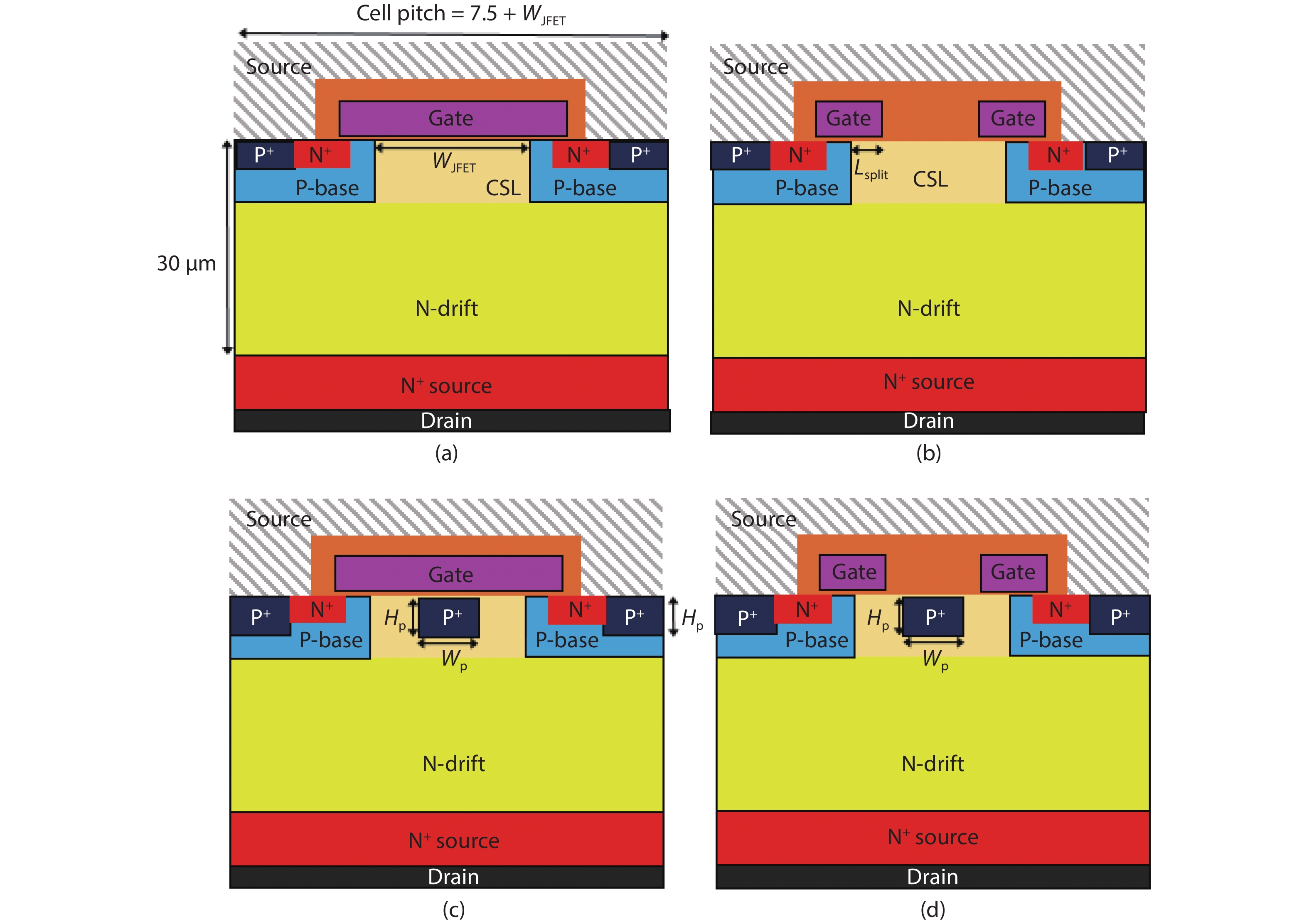
Fig. 1.
(Color online) Schematic cross-sectional views of the MOSFETs. (a) Planar MOSFET. (b) SG-MOSFET. (c) CIMOSFET. (d) SG-CIMOSFET.
ARTICLES
Jongwoon Yoon and Kwangsoo Kim
Corresponding author: Kwangsoo Kim, kimks@sogang.ac.kr
Abstract: A split gate MOSFET (SG-MOSFET) is widely known for reducing the reverse transfer capacitance (CRSS). In a 3.3 kV class, the SG-MOSFET does not provide reliable operation due to the high gate oxide electric field. In addition to the poor static performance, the SG-MOSFET has issues such as the punch through and drain-induced barrier lowering (DIBL) caused by the high gate oxide electric field. As such, a 3.3 kV 4H-SiC split gate MOSFET with a grounded central implant region (SG-CIMOSFET) is proposed to resolve these issues and for achieving a superior trade-off between the static and switching performance. The SG-CIMOSFET has a significantly low on-resistance (RON) and maximum gate oxide field (EOX) due to the central implant region. A grounded central implant region significantly reduces the CRSS and gate drain charge (QGD) by partially screening the gate-to-drain capacitive coupling. Compared to a planar MOSFET, the SG MOSFET, central implant MOSFET (CIMOSFET), the SG-CIMOSFET improve the RON×QGD by 83.7%, 72.4% and 44.5%, respectively. The results show that the device features not only the smallest switching energy loss but also the fastest switching time.
Key words: 4H-SiC, split gate, on-resistance, reverse transfer capacitance, switching energy loss, switching time
| [1] |
Baliga B J. Power MOSFETs Fundamentals of power semiconductor devices. Boston, MA: Springer US, 2008, 276
|
| [2] |
Ji S Q, Zhang Z Y, Wang F. Overview of high voltage sic power semiconductor devices: Development and application. CES Trans Electr Mach Syst, 2017, 1, 254 doi: 10.23919/TEMS.2017.8086104
|
| [3] |
Cooper J A, Agarwal A. SiC power-switching devices-the second electronics revolution. Proc IEEE, 2002, 90, 956 doi: 10.1109/JPROC.2002.1021561
|
| [4] |
Wang G Y, Wang F, Magai G R, et al. Performance comparison of 1200V 100A SiC MOSFET and 1200V 100A silicon IGBT. 2013 IEEE Energy Convers Congr Expo, 2013, 3230
|
| [5] |
Nakamura T, Nakano Y, Aketa M, et al. High performance SiC trench devices with ultra-low Ron. 2011 International Electron Devices Meeting, 2011, 26.5.1
|
| [6] |
Sampath M, Morisette D T, Cooper J A. Comparison of single- and double-trench UMOSFETs in 4H-SiC. Mater Sci Forum, 2018, 924, 752 doi: 10.4028/www.scientific.net/MSF.924.752
|
| [7] |
Krishnaswami S, Das M, Hull B, et al. Gate oxide reliability of 4H-SiC MOS devices. 2005 IEEE International Reliability Physics Symposium, 2005, 592
|
| [8] |
Xu S M, Ren C H, Liang Y C, et al. Theoretical analysis and experimental characterization of the dummy-gated VDMOSFET. IEEE Trans Electron Devices, 2001, 48, 2168 doi: 10.1109/16.944212
|
| [9] |
Agarwal A, Han K, Baliga B J. 2.3 kV 4H-SiC accumulation-channel split-gate planar power MOSFETs with reduced gate charge. IEEE J Electron Devices Soc, 2020, 8, 499 doi: 10.1109/JEDS.2020.2991355
|
| [10] |
Han K, Baliga B J, Sung W. A novel 1.2 kV 4H-SiC buffered-gate (BG) MOSFET: Analysis and experimental results. IEEE Electron Device Lett, 2018, 39, 248 doi: 10.1109/LED.2017.2785771
|
| [11] |
Vudumula P, Kotamraju S. Design and optimization of 1.2-kV SiC planar inversion MOSFET using split dummy gate concept for high-frequency applications. IEEE Trans Electron Devices, 2019, 66, 5266 doi: 10.1109/TED.2019.2949459
|
| [12] |
Zhang Q C J, Duc J, Hull B, et al. CIMOSFET: A new MOSFET on SiC with a superior Ron·Qgd figure of merit. Mater Sci Forum, 2015, 821–823, 765
|
| [13] |
Zhang Q J, Wang G Y, Doan H, et al. Latest results on 1200 V 4H-SiC CIMOSFETs with Rsp, on of 3.9 mΩ·cm2 at 150 °C. 2015 IEEE 27th International Symposium on Power Semiconductor Devices & IC's (ISPSD), 2015, 89
|
| [14] |
TCAD Sentaurus Device Manual, Synopsys. 2016, Inc., Mountain View, CA, USA
|
| [15] |
Darwish M N, Lentz J L, Pinto M R, et al. An improved electron and hole mobility model for general purpose device simulation. IEEE Trans Electron Devices, 1997, 44, 1529 doi: 10.1109/16.622611
|
| [16] |
Mujtaba S A. Advanced mobility models for design and simulation of deep submicrometer MOSFETs. PhD Dissertation, Stanford University, 1995
|
| [17] |
Han K, Baliga B J, Sung W. Split-gate 1.2-kV 4H-SiC MOSFET: Analysis and experimental validation. IEEE Electron Device Lett, 2017, 38, 1437 doi: 10.1109/LED.2017.2738616
|
| [18] |
Wei J, Zhang M, Jiang H P, et al. Low ON-resistance SiC trench/planar MOSFET with reduced OFF-state oxide field and low gate charges. IEEE Electron Device Lett, 2016, 37, 1458 doi: 10.1109/LED.2016.2609599
|
| [19] |
Wei J, Zhang M, Jiang H P, et al. Dynamic degradation in SiC trench MOSFET with a floating p-shield revealed with numerical simulations. IEEE Trans Electron Devices, 2017, 64, 2592 doi: 10.1109/TED.2017.2697763
|
| [20] |
Ren M, Chen Z, Niu B, et al. A low miller capacitance VDMOS with shield gate and oxide trench. 2016 IEEE International Nanoelectronics Conference (INEC), 2016, 1
|
| [21] |
Basler T, Heer D, Peters D, et al. Practical aspects and body diode robustness of a 1200 V SiC trench MOSFET. International Exhibition and Conference for Power Electronics, Intelligent Motion, Renewable Energy and Energy Management, 2018, 1
|
| [22] |
Maerz A, Bertelshofer T, Bakran M, et al. A novel gate drive concept to eliminate parasitic turn-on of SiC MOSFET in low inductance power modules. International Exhibition and Conference for Power Electronics, Intelligent Motion, Renewable Energy and Energy Management, 2017, 1
|
| [23] |
Tian K, Hallén A, Qi J W, et al. An improved 4H-SiC trench-gate MOSFET with low ON-resistance and switching loss. IEEE Trans Electron Devices, 2019, 66, 2307 doi: 10.1109/TED.2019.2905636
|
| [24] |
Morikawa T, Ishigaki T, Shima A. Device design consideration for robust SiC VDMOSFET with self-aligned channels formed by tilted implantation. IEEE Trans Electron Devices, 2019, 66, 3447 doi: 10.1109/TED.2019.2924969
|
| [25] |
Zhou X T, Yue R F, Zhang J, et al. 4H-SiC trench MOSFET with floating/grounded junction barrier-controlled gate structure. IEEE Trans Electron Devices, 2017, 64, 4568 doi: 10.1109/TED.2017.2755721
|
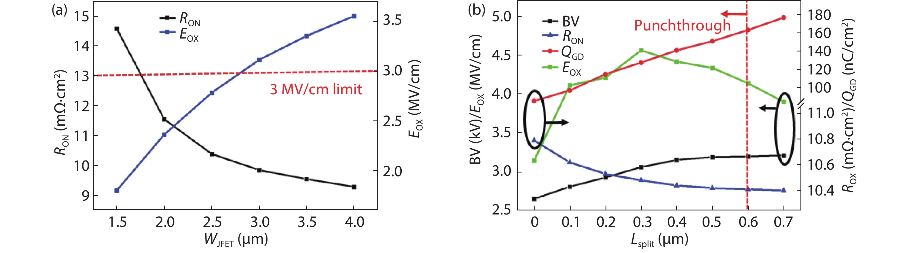

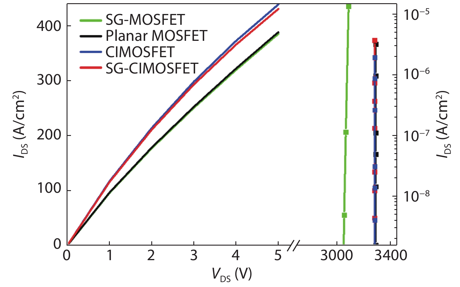
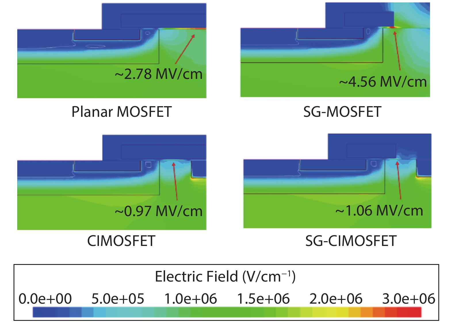
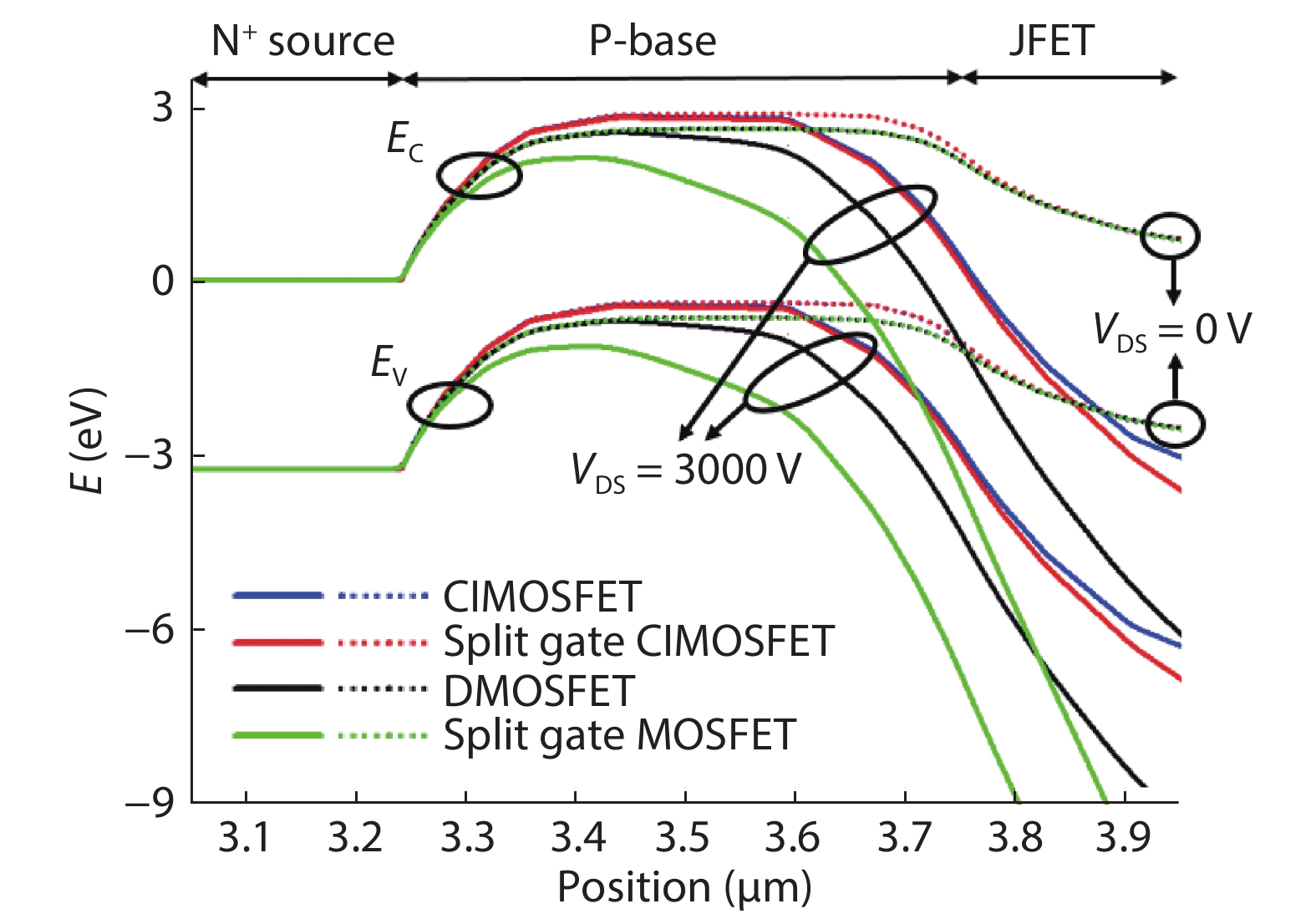
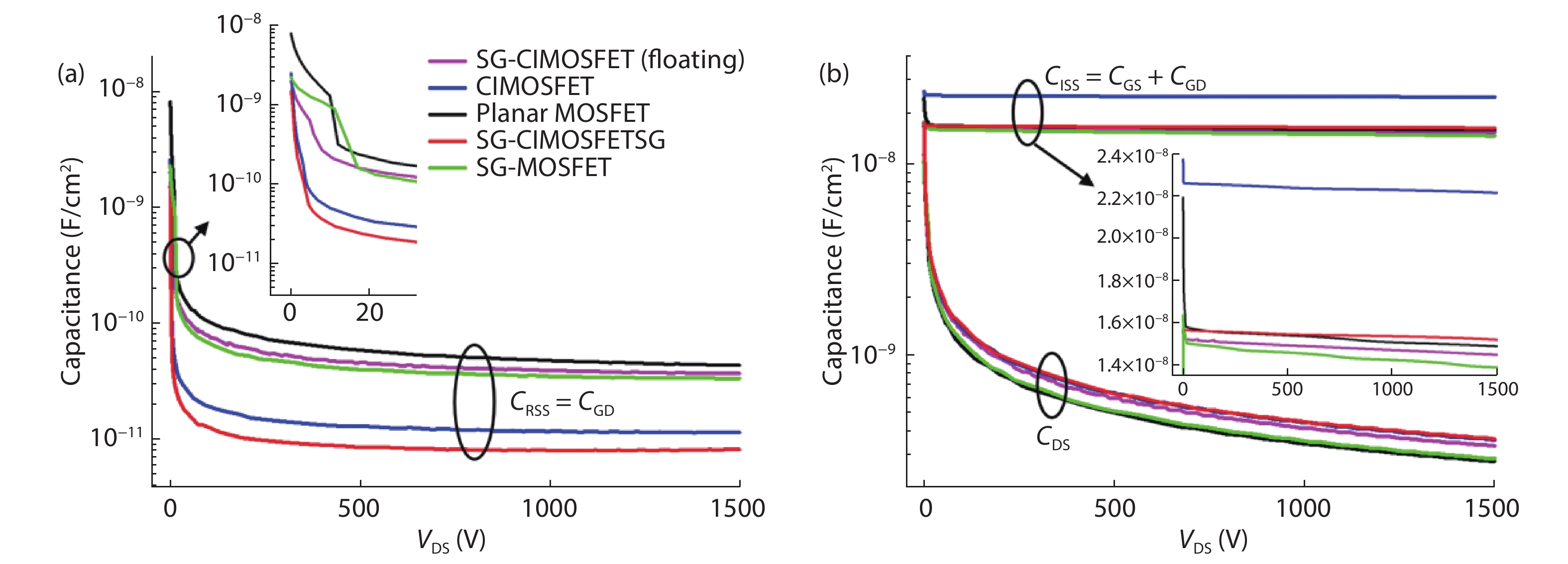
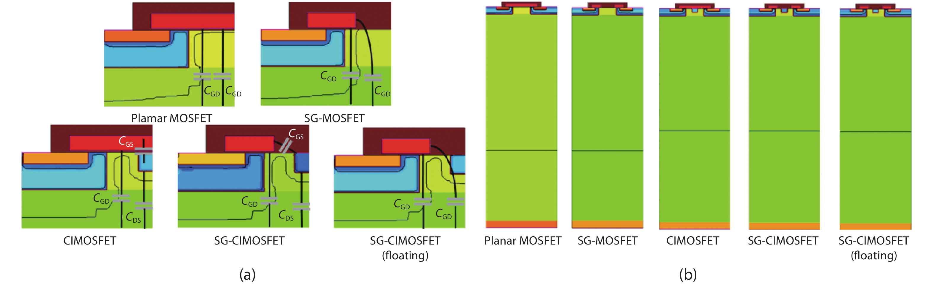


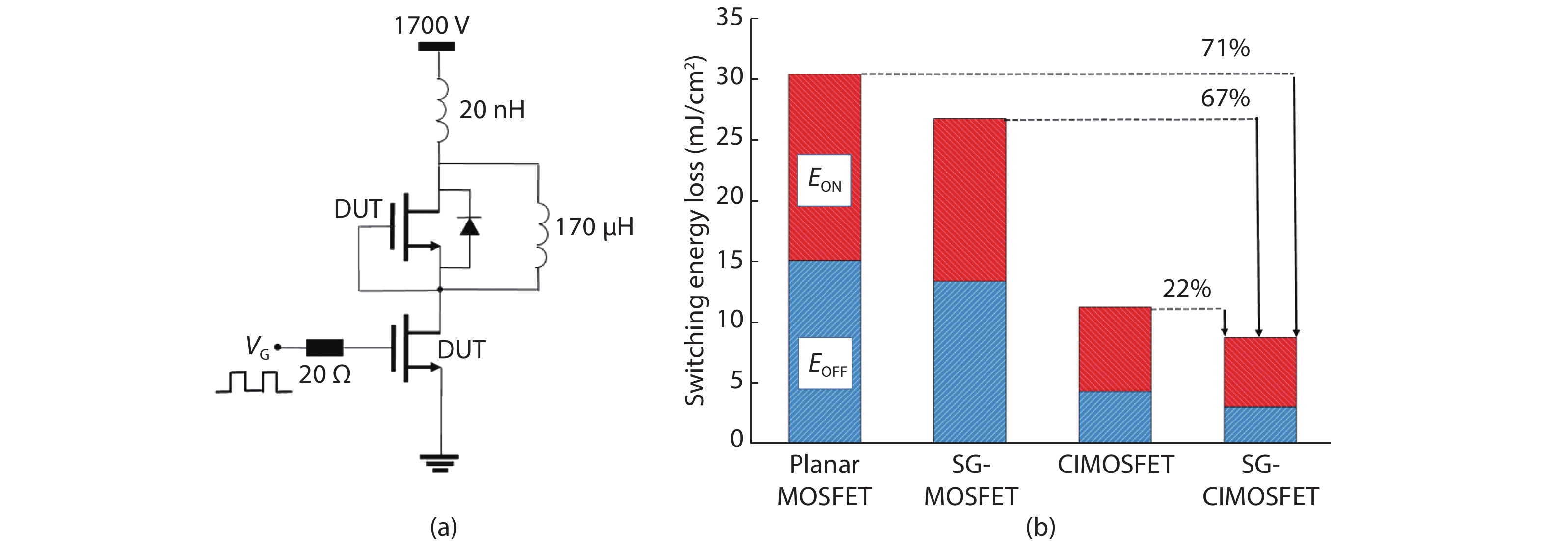
Table 1. Device characteristics comparison.
| Parameter | Planar MOSFET | SG-MOSFET | CI-MOSFET | SG-CIMOSFET | Unit |
| N-drift doping concentration | 2.2 × 10¹⁵ | 2.2 × 10¹⁵ | 3 × 10¹⁵ | 3 × 10¹⁵ | cm–3 |
| RON a | 10.39 | 10.49 | 8.59 | 8.67 | mΩ∙cm2 |
| EOX b | 2.78 | 4.56 | 0.97 | 1.06 | MV/cm |
| QG c | 754.06 | 503.62 | 651.56 | 424.85 | nC/cm2 |
| QGD | 216.92 | 126.98 | 77.21 | 42.49 | nC/cm2 |
| QTH | 72.32 | 60.95 | 112.48 | 80.12 | nC/cm2 |
| QGD/QTH | 2.99 | 2.08 | 0.69 | 0.53 | |
| CRSS d | 42.27 | 32.19 | 11.16 | 7.72 | pF/cm2 |
| CISS d | 14.99 | 13.93 | 22.31 | 15.21 | nF/cm2 |
| COSS d | 316.21 | 315.78 | 365.96 | 365.96 | nF/cm2 |
| RON×QGD | 2254 | 1332 | 663 | 368 | mΩ∙nC |
| RON×QG | 7834 | 5282 | 5597 | 3683 | mΩ∙nC |
| RON×CRSS | 439 | 338 | 96 | 67 | mΩ∙pF |
| a RON at VGS = 20 V, b EOX at VDS = 3000 V, c QG is the total gate charge, which is the gate charge from VGS = 0 to 20 V. d CISS, COSS, and CRSS are measured at VDS = 1500 V. | |||||
 DownLoad: CSV
Table 2. Switching characteristics comparison.
| Parameter | Planar | SG- | CI- | SG-CI | Unit |
| TD-OFF | 795.4 | 540.6 | 603.6 | 363.1 | ns |
| TF | 171.3 | 151.1 | 61.5 | 46.1 | ns |
| TOFF | 966.7 | 691.7 | 665.1 | 409.2 | ns |
| TD-ON | 159.2 | 146.1 | 227.5 | 154.1 | ns |
| TR | 134.2 | 115.6 | 48.2 | 36.4 | ns |
| TON | 293.4 | 261.7 | 275.7 | 190.5 | ns |
| EOFF | 15.1 | 13.4 | 4.4 | 3.1 | mJ/cm2 |
| EON | 15.3 | 13.4 | 6.9 | 5.7 | mJ/cm2 |
| ETOTAL a | 30.4 | 26.8 | 11.3 | 8.8 | mJ/cm2 |
| a | |||||
DownLoad: CSV
| [1] |
Baliga B J. Power MOSFETs Fundamentals of power semiconductor devices. Boston, MA: Springer US, 2008, 276
|
| [2] |
Ji S Q, Zhang Z Y, Wang F. Overview of high voltage sic power semiconductor devices: Development and application. CES Trans Electr Mach Syst, 2017, 1, 254 doi: 10.23919/TEMS.2017.8086104
|
| [3] |
Cooper J A, Agarwal A. SiC power-switching devices-the second electronics revolution. Proc IEEE, 2002, 90, 956 doi: 10.1109/JPROC.2002.1021561
|
| [4] |
Wang G Y, Wang F, Magai G R, et al. Performance comparison of 1200V 100A SiC MOSFET and 1200V 100A silicon IGBT. 2013 IEEE Energy Convers Congr Expo, 2013, 3230
|
| [5] |
Nakamura T, Nakano Y, Aketa M, et al. High performance SiC trench devices with ultra-low Ron. 2011 International Electron Devices Meeting, 2011, 26.5.1
|
| [6] |
Sampath M, Morisette D T, Cooper J A. Comparison of single- and double-trench UMOSFETs in 4H-SiC. Mater Sci Forum, 2018, 924, 752 doi: 10.4028/www.scientific.net/MSF.924.752
|
| [7] |
Krishnaswami S, Das M, Hull B, et al. Gate oxide reliability of 4H-SiC MOS devices. 2005 IEEE International Reliability Physics Symposium, 2005, 592
|
| [8] |
Xu S M, Ren C H, Liang Y C, et al. Theoretical analysis and experimental characterization of the dummy-gated VDMOSFET. IEEE Trans Electron Devices, 2001, 48, 2168 doi: 10.1109/16.944212
|
| [9] |
Agarwal A, Han K, Baliga B J. 2.3 kV 4H-SiC accumulation-channel split-gate planar power MOSFETs with reduced gate charge. IEEE J Electron Devices Soc, 2020, 8, 499 doi: 10.1109/JEDS.2020.2991355
|
| [10] |
Han K, Baliga B J, Sung W. A novel 1.2 kV 4H-SiC buffered-gate (BG) MOSFET: Analysis and experimental results. IEEE Electron Device Lett, 2018, 39, 248 doi: 10.1109/LED.2017.2785771
|
| [11] |
Vudumula P, Kotamraju S. Design and optimization of 1.2-kV SiC planar inversion MOSFET using split dummy gate concept for high-frequency applications. IEEE Trans Electron Devices, 2019, 66, 5266 doi: 10.1109/TED.2019.2949459
|
| [12] |
Zhang Q C J, Duc J, Hull B, et al. CIMOSFET: A new MOSFET on SiC with a superior Ron·Qgd figure of merit. Mater Sci Forum, 2015, 821–823, 765
|
| [13] |
Zhang Q J, Wang G Y, Doan H, et al. Latest results on 1200 V 4H-SiC CIMOSFETs with Rsp, on of 3.9 mΩ·cm2 at 150 °C. 2015 IEEE 27th International Symposium on Power Semiconductor Devices & IC's (ISPSD), 2015, 89
|
| [14] |
TCAD Sentaurus Device Manual, Synopsys. 2016, Inc., Mountain View, CA, USA
|
| [15] |
Darwish M N, Lentz J L, Pinto M R, et al. An improved electron and hole mobility model for general purpose device simulation. IEEE Trans Electron Devices, 1997, 44, 1529 doi: 10.1109/16.622611
|
| [16] |
Mujtaba S A. Advanced mobility models for design and simulation of deep submicrometer MOSFETs. PhD Dissertation, Stanford University, 1995
|
| [17] |
Han K, Baliga B J, Sung W. Split-gate 1.2-kV 4H-SiC MOSFET: Analysis and experimental validation. IEEE Electron Device Lett, 2017, 38, 1437 doi: 10.1109/LED.2017.2738616
|
| [18] |
Wei J, Zhang M, Jiang H P, et al. Low ON-resistance SiC trench/planar MOSFET with reduced OFF-state oxide field and low gate charges. IEEE Electron Device Lett, 2016, 37, 1458 doi: 10.1109/LED.2016.2609599
|
| [19] |
Wei J, Zhang M, Jiang H P, et al. Dynamic degradation in SiC trench MOSFET with a floating p-shield revealed with numerical simulations. IEEE Trans Electron Devices, 2017, 64, 2592 doi: 10.1109/TED.2017.2697763
|
| [20] |
Ren M, Chen Z, Niu B, et al. A low miller capacitance VDMOS with shield gate and oxide trench. 2016 IEEE International Nanoelectronics Conference (INEC), 2016, 1
|
| [21] |
Basler T, Heer D, Peters D, et al. Practical aspects and body diode robustness of a 1200 V SiC trench MOSFET. International Exhibition and Conference for Power Electronics, Intelligent Motion, Renewable Energy and Energy Management, 2018, 1
|
| [22] |
Maerz A, Bertelshofer T, Bakran M, et al. A novel gate drive concept to eliminate parasitic turn-on of SiC MOSFET in low inductance power modules. International Exhibition and Conference for Power Electronics, Intelligent Motion, Renewable Energy and Energy Management, 2017, 1
|
| [23] |
Tian K, Hallén A, Qi J W, et al. An improved 4H-SiC trench-gate MOSFET with low ON-resistance and switching loss. IEEE Trans Electron Devices, 2019, 66, 2307 doi: 10.1109/TED.2019.2905636
|
| [24] |
Morikawa T, Ishigaki T, Shima A. Device design consideration for robust SiC VDMOSFET with self-aligned channels formed by tilted implantation. IEEE Trans Electron Devices, 2019, 66, 3447 doi: 10.1109/TED.2019.2924969
|
| [25] |
Zhou X T, Yue R F, Zhang J, et al. 4H-SiC trench MOSFET with floating/grounded junction barrier-controlled gate structure. IEEE Trans Electron Devices, 2017, 64, 4568 doi: 10.1109/TED.2017.2755721
|


Article views: 2861 Times PDF downloads: 137 Times Cited by: 0 Times
Received: 04 November 2020 Revised: 12 January 2021 Online: Accepted Manuscript: 18 March 2021Uncorrected proof: 12 April 2021Published: 01 June 2021
| Citation: |
Jongwoon Yoon, Kwangsoo Kim. A 3.3 kV 4H-SiC split gate MOSFET with a central implant region for superior trade-off between static and switching performance[J]. Journal of Semiconductors, 2021, 42(6): 062803. doi: 10.1088/1674-4926/42/6/062803
J Yoon, K Kim, A 3.3 kV 4H-SiC split gate MOSFET with a central implant region for superior trade-off between static and switching performance[J]. J. Semicond., 2021, 42(6): 062803. doi: 10.1088/1674-4926/42/6/062803.
Export: BibTex EndNote

|
| [1] |
Baliga B J. Power MOSFETs Fundamentals of power semiconductor devices. Boston, MA: Springer US, 2008, 276
|
| [2] |
Ji S Q, Zhang Z Y, Wang F. Overview of high voltage sic power semiconductor devices: Development and application. CES Trans Electr Mach Syst, 2017, 1, 254 doi: 10.23919/TEMS.2017.8086104
|
| [3] |
Cooper J A, Agarwal A. SiC power-switching devices-the second electronics revolution. Proc IEEE, 2002, 90, 956 doi: 10.1109/JPROC.2002.1021561
|
| [4] |
Wang G Y, Wang F, Magai G R, et al. Performance comparison of 1200V 100A SiC MOSFET and 1200V 100A silicon IGBT. 2013 IEEE Energy Convers Congr Expo, 2013, 3230
|
| [5] |
Nakamura T, Nakano Y, Aketa M, et al. High performance SiC trench devices with ultra-low Ron. 2011 International Electron Devices Meeting, 2011, 26.5.1
|
| [6] |
Sampath M, Morisette D T, Cooper J A. Comparison of single- and double-trench UMOSFETs in 4H-SiC. Mater Sci Forum, 2018, 924, 752 doi: 10.4028/www.scientific.net/MSF.924.752
|
| [7] |
Krishnaswami S, Das M, Hull B, et al. Gate oxide reliability of 4H-SiC MOS devices. 2005 IEEE International Reliability Physics Symposium, 2005, 592
|
| [8] |
Xu S M, Ren C H, Liang Y C, et al. Theoretical analysis and experimental characterization of the dummy-gated VDMOSFET. IEEE Trans Electron Devices, 2001, 48, 2168 doi: 10.1109/16.944212
|
| [9] |
Agarwal A, Han K, Baliga B J. 2.3 kV 4H-SiC accumulation-channel split-gate planar power MOSFETs with reduced gate charge. IEEE J Electron Devices Soc, 2020, 8, 499 doi: 10.1109/JEDS.2020.2991355
|
| [10] |
Han K, Baliga B J, Sung W. A novel 1.2 kV 4H-SiC buffered-gate (BG) MOSFET: Analysis and experimental results. IEEE Electron Device Lett, 2018, 39, 248 doi: 10.1109/LED.2017.2785771
|
| [11] |
Vudumula P, Kotamraju S. Design and optimization of 1.2-kV SiC planar inversion MOSFET using split dummy gate concept for high-frequency applications. IEEE Trans Electron Devices, 2019, 66, 5266 doi: 10.1109/TED.2019.2949459
|
| [12] |
Zhang Q C J, Duc J, Hull B, et al. CIMOSFET: A new MOSFET on SiC with a superior Ron·Qgd figure of merit. Mater Sci Forum, 2015, 821–823, 765
|
| [13] |
Zhang Q J, Wang G Y, Doan H, et al. Latest results on 1200 V 4H-SiC CIMOSFETs with Rsp, on of 3.9 mΩ·cm2 at 150 °C. 2015 IEEE 27th International Symposium on Power Semiconductor Devices & IC's (ISPSD), 2015, 89
|
| [14] |
TCAD Sentaurus Device Manual, Synopsys. 2016, Inc., Mountain View, CA, USA
|
| [15] |
Darwish M N, Lentz J L, Pinto M R, et al. An improved electron and hole mobility model for general purpose device simulation. IEEE Trans Electron Devices, 1997, 44, 1529 doi: 10.1109/16.622611
|
| [16] |
Mujtaba S A. Advanced mobility models for design and simulation of deep submicrometer MOSFETs. PhD Dissertation, Stanford University, 1995
|
| [17] |
Han K, Baliga B J, Sung W. Split-gate 1.2-kV 4H-SiC MOSFET: Analysis and experimental validation. IEEE Electron Device Lett, 2017, 38, 1437 doi: 10.1109/LED.2017.2738616
|
| [18] |
Wei J, Zhang M, Jiang H P, et al. Low ON-resistance SiC trench/planar MOSFET with reduced OFF-state oxide field and low gate charges. IEEE Electron Device Lett, 2016, 37, 1458 doi: 10.1109/LED.2016.2609599
|
| [19] |
Wei J, Zhang M, Jiang H P, et al. Dynamic degradation in SiC trench MOSFET with a floating p-shield revealed with numerical simulations. IEEE Trans Electron Devices, 2017, 64, 2592 doi: 10.1109/TED.2017.2697763
|
| [20] |
Ren M, Chen Z, Niu B, et al. A low miller capacitance VDMOS with shield gate and oxide trench. 2016 IEEE International Nanoelectronics Conference (INEC), 2016, 1
|
| [21] |
Basler T, Heer D, Peters D, et al. Practical aspects and body diode robustness of a 1200 V SiC trench MOSFET. International Exhibition and Conference for Power Electronics, Intelligent Motion, Renewable Energy and Energy Management, 2018, 1
|
| [22] |
Maerz A, Bertelshofer T, Bakran M, et al. A novel gate drive concept to eliminate parasitic turn-on of SiC MOSFET in low inductance power modules. International Exhibition and Conference for Power Electronics, Intelligent Motion, Renewable Energy and Energy Management, 2017, 1
|
| [23] |
Tian K, Hallén A, Qi J W, et al. An improved 4H-SiC trench-gate MOSFET with low ON-resistance and switching loss. IEEE Trans Electron Devices, 2019, 66, 2307 doi: 10.1109/TED.2019.2905636
|
| [24] |
Morikawa T, Ishigaki T, Shima A. Device design consideration for robust SiC VDMOSFET with self-aligned channels formed by tilted implantation. IEEE Trans Electron Devices, 2019, 66, 3447 doi: 10.1109/TED.2019.2924969
|
| [25] |
Zhou X T, Yue R F, Zhang J, et al. 4H-SiC trench MOSFET with floating/grounded junction barrier-controlled gate structure. IEEE Trans Electron Devices, 2017, 64, 4568 doi: 10.1109/TED.2017.2755721
|

 WeChat ID
Journal of Semiconductors © 2017 All Rights Reserved 京ICP备05085259号-2


