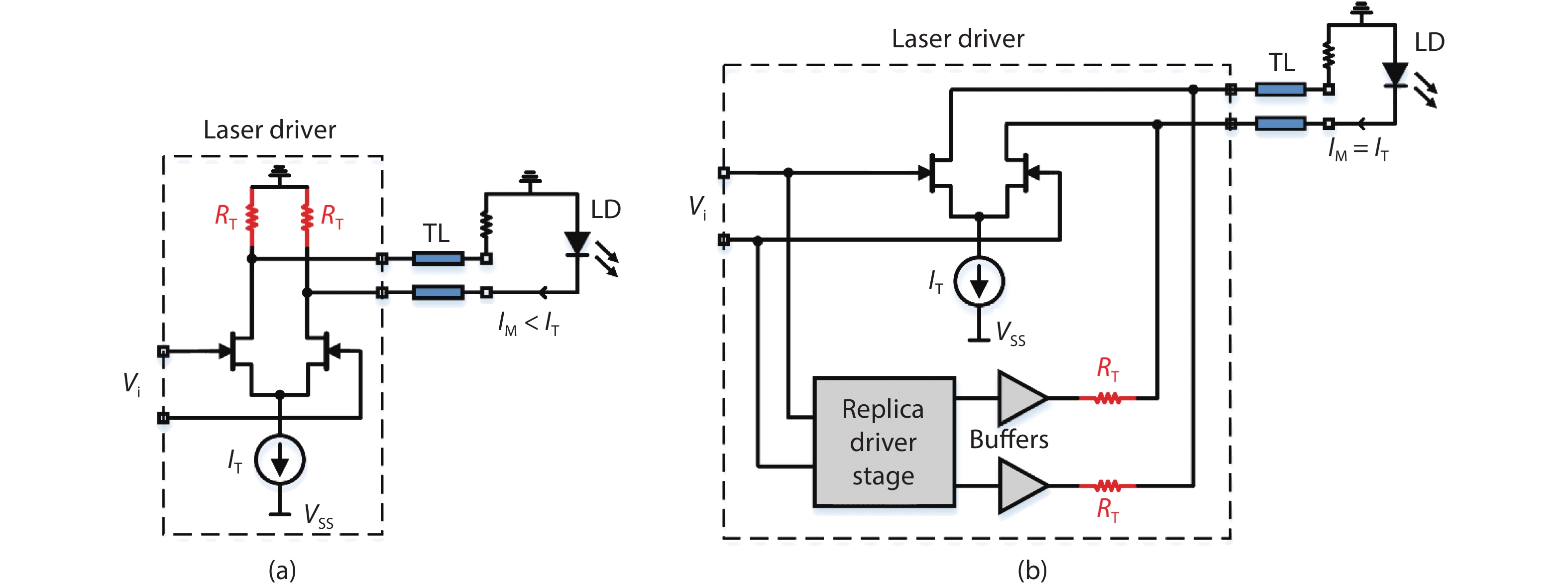
Fig. 1.
LDD output stage: (a) with passive back termination, (b) with active back termination.
ARTICLES
Ahmed Wahba, Lin Cheng and Fujiang Lin
Corresponding author: Fujiang Lin, linfj@ustc.edu.cn
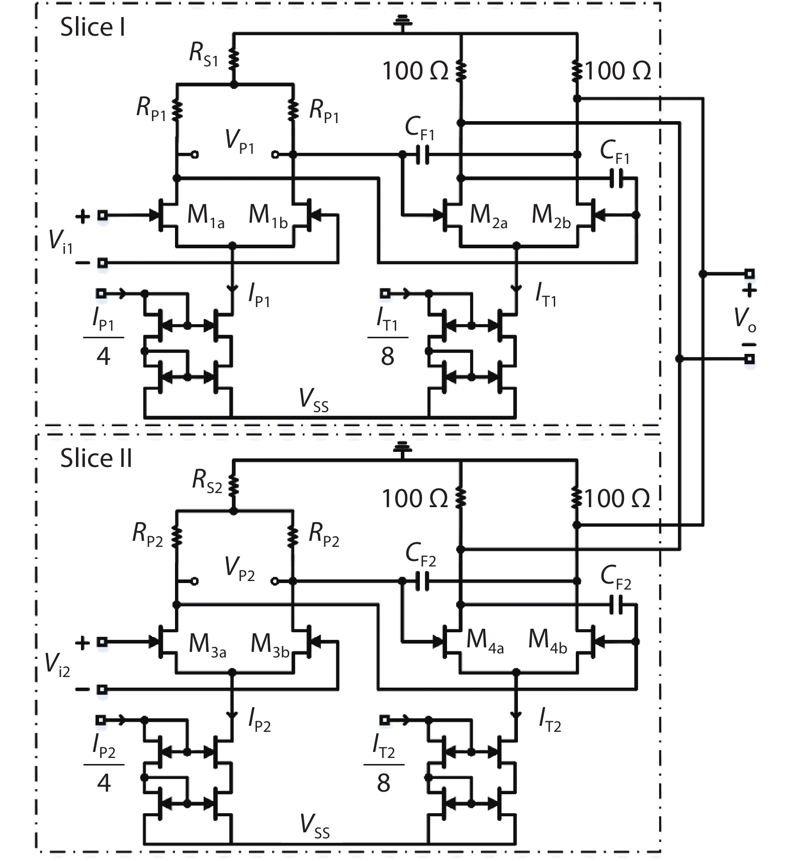
Abstract: This paper presents the design and testing of a 15 Gbps non-return-to-zero (NRZ), 30 Gbps 4-level pulse amplitude modulation (PAM4) configurable laser diode driver (LDD) implemented in 0.15-µm GaAs E-mode pHEMT technology. The driver bandwidth is enhanced by utilizing cross-coupled neutralization capacitors across the output stage. The output transmission-line back-termination, which absorbs signal reflections from the imperfectly matched load, is performed passively with on-chip 50-Ω resistors. The proposed 30 Gbps PAM4 LDD is implemented by combining two 15 Gbps-NRZ LDDs, as the high and low amplification paths, to generate PAM4 output current signal with levels of 0, 40, 80, and 120 mA when driving 25-Ω lasers. The high and low amplification paths can be used separately or simultaneously as a 15 Gbps-NRZ LDD. The measurement results show clear output eye diagrams at speeds of up to 15 and 30 Gbps for the NRZ and PAM4 drivers, respectively. At a maximum output current of 120 mA, the driver consumes 1.228 W from a single supply voltage of –5.2 V. The proposed driver shows a high current driving capability with a better output power to power dissipation ratio, which makes it suitable for driving high current distributed feedback (DFB) lasers. The chip occupies a total area of 0.7 × 1.3 mm2.
Key words: high current drivers, impedance matching, laser diode driver, optical transmitter, NRZ, PAM4, pHEMT technology.
| [1] |
Razavi B. Design of integrated circuits for optical communications. 2nd ed. Hoboken, New Jersey: WILEY, 2012
|
| [2] |
Morley S. A 3 V 10.7 Gb/s differential laser diode driver with active back-termination output stage. 2005 IEEE International Solid-State Circuits Conference, 2005, 220
|
| [3] |
Tsai C M, Chiu M C. A 10Gb/s laser-diode driver with active back-termination in 0.18 μm CMOS. 2008 IEEE International Solid-State Circuits Conference - Digest of Technical Papers, 2008, 222
|
| [4] |
Galal S, Razavi B. 10-Gb/s limiting amplifier and laser/modulator driver in 0.18-μm CMOS technology. IEEE J Solid-State Circuits, 2003, 38, 2138 doi: 10.1109/JSSC.2003.818567
|
| [5] |
Chiang P C, Jiang J Y, Hung H W, et al. 4 × 25 Gb/s transceiver with optical front-end for 100 GbE system in 65 nm CMOS technology. IEEE J Solid-State Circuits, 2015, 50, 573 doi: 10.1109/JSSC.2014.2365700
|
| [6] |
Takemoto T, Matsuoka Y, Sugiyama Y, et al. A 50-Gb/s NRZ-modulated optical transmitter based on a DFB-LD and a 0.18-μm SiGe BiCMOS LD driver. Optical Fiber Communication Conference, 2015, 1
|
| [7] |
Huang T, Wang Z G, Zhu E, et al. 24 Gb/s laser/modulator driver IC using 0.2 μm gate length PHEMTs. ESSCIRC 2004 - 29th European Solid-State Circuits Conference, 2003, 277
|
| [8] |
Takemoto T, Yamashita H, Yuki F, et al. A 25-Gb/s 2.2-W 65-nm CMOS optical transceiver using a power-supply-variation-tolerant analog front end and data-format conversion. IEEE J Solid-State Circuits, 2014, 49, 471 doi: 10.1109/JSSC.2013.2291099
|
| [9] |
Ransijn H, Salvador G, Daugherty D D, et al. A 10-Gb/s laser/modulator driver IC with a dual-mode actively matched output buffer. IEEE J Solid-State Circuits, 2001, 36, 1314 doi: 10.1109/4.944657
|
| [10] |
Fattaruso J W, Sheahan B. A 3-V 4.25-Gb/s laser driver with 0.4-V output voltage compliance. IEEE J Solid-State Circuits, 2006, 41, 1930 doi: 10.1109/JSSC.2006.875288
|
| [11] |
Yin B Z, Qi N, Shi J B, et al. A 32Gb/s-NRZ, 15GBaud/s-PAM4 DFB laser driver with active back-termination in 65 nm CMOS. 2017 IEEE Radio Frequency Integrated Circuits Symposium (RFIC), 2017, 264
|
| [12] |
Shi J B, Yin B Z, Qi N, et al. Design techniques for signal reflection suppression in high-speed 25-Gb/s laser drivers in CMOS. IEEE Photonics Technol Lett, 2018, 30, 39 doi: 10.1109/LPT.2017.2773525
|
| [13] |
Miyashita M, Yoshida N, Kojima Y, et al. An AlGaAs/InGaAs pseudomorphic HEMT modulator driver IC with low power dissipation for 10-Gb/s optical transmission systems. IEEE Trans Microw Theory Tech, 1997, 45, 1058 doi: 10.1109/22.598441
|
| [14] |
Bauwelinck J, Chen W, Verhulst D, et al. A high-resolution burst-mode laser transmitter with fast and accurate level monitoring for 1.25 Gb/s upstream GPONs. IEEE J Solid-State Circuits, 2005, 40, 1322 doi: 10.1109/JSSC.2005.848024
|
| [15] |
Umeda Y, Kanda A, Sano K, et al. 10 Gbit/s series-connected voltage-balancing pulse driver with high-speed input buffer. Electron Lett, 2004, 40, 934 doi: 10.1049/el:20045223
|
| [16] |
Chujo N, Takai T, Sugawara T, et al. A 25 Gb/s 65-nm CMOS low-power laser diode driver with mutually coupled peaking inductors for optical interconnects. IEEE Trans Circuits Syst I, 2011, 58, 2061 doi: 10.1109/TCSI.2011.2163982
|
| [17] |
Schow C L, Doany F E, Chen C, et al. Low-power 16 × 10 Gb/s Bi-directional single chip CMOS optical transceivers operating at < < 5 mW/Gb/s/link. IEEE J Solid-State Circuits, 2009, 44, 301 doi: 10.1109/JSSC.2008.2007439
|
| [18] |
Kromer C, Sialm G, Berger C, et al. A 100-mW 4 × 10 Gb/s transceiver in 80-nm CMOS for high-density optical interconnects. IEEE J Solid-State Circuits, 2005, 40, 2667 doi: 10.1109/JSSC.2005.856575
|
| [19] |
Wahba A, Li X, Xi N, et al. A 10 gb/s, 150 mA laser diode driver with active back-termination in 0.13-µm SOI CMOS technology. 2019 IEEE International Conference on Integrated Circuits, Technologies and Applications, 2019, 91
|
| [20] |
Belfiore G, Henker R, Ellinger F. 90 Gbit/s 4-level pulse-amplitude-modulation vertical-cavity surface-emitting laser driver integrated circuit in 130 nm SiGe technology. 2016 IEEE MTT-S Latin America Microwave Conference (LAMC), 2016, 1
|
| [21] |
Belfiore G, Szilagyi L, Henker R, et al. Design of a 56 Gbit/s 4-level pulse-amplitude-modulation inductor-less vertical-cavity surface-emitting laser driver integrated circuit in 130 nm BiCMOS technology. IET Circuits Devices Syst, 2015, 9, 213 doi: 10.1049/iet-cds.2014.0240
|
| [22] |
Belfiore G, Szilagyi L, Henker R, et al. Common cathode VCSEL driver in 90 nm CMOS enabling 25 Gbit/s optical connection using 14 Gbit/s 850 nm VCSEL. Electron Lett, 2015, 51, 349 doi: 10.1049/el.2014.4217
|
| [23] |
Gray P R, Hurst P J, Lewis S H, et al. Analysis and design of analog integrated circuits. John Wiley & Sons, 2009
|
| [24] |
Säckinger E. Broadband circuits for optical fiber communication. Hoboken, NJ, USA: John Wiley & Sons, Inc., 2005
|
| [25] |
Heydari P, Mohanavelu R. Design of ultrahigh-speed low-voltage CMOS CML buffers and latches. IEEE Trans Very Large Scale Integr VLSI Syst, 2004, 12, 1081 doi: 10.1109/TVLSI.2004.833663
|
| [26] |
Lao Z, Thiede A, Nowotny U, et al. High power modulator driver ICs up to 30 Gb/s with AlGaAs/GaAs HEMTs. IEEE Gallium Arsenide Integrated Circuit Symposium, 1997, 223
|
| [27] |
Zhu N H, Chen C, Pun E Y B, et al. Extraction of intrinsic response from S-parameters of laser diodes. IEEE Photonics Technol Lett, 2005, 17, 744 doi: 10.1109/LPT.2004.842794
|
| [28] |
Chen C, Zhu N, Zhang S, et al. Characterization of parasitics in TO-packaged high-speed laser modules. IEEE Trans Adv Packag, 2007, 30, 97 doi: 10.1109/TADVP.2006.884779
|
| [29] |
Gao J J. Optoelectronic integrated circuit design and device modeling. Chichester, UK: John Wiley & Sons, Ltd, 2010
|
| [30] |
Khafaji M, Pliva J, Henker R, et al. A 42-Gb/s VCSEL driver suitable for burst mode operation in 14-nm bulk CMOS. IEEE Photonics Technol Lett, 2018, 30, 23 doi: 10.1109/LPT.2017.2771952
|
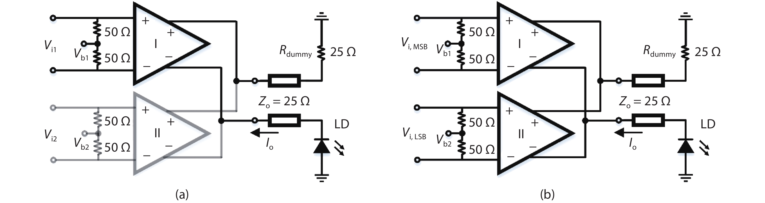


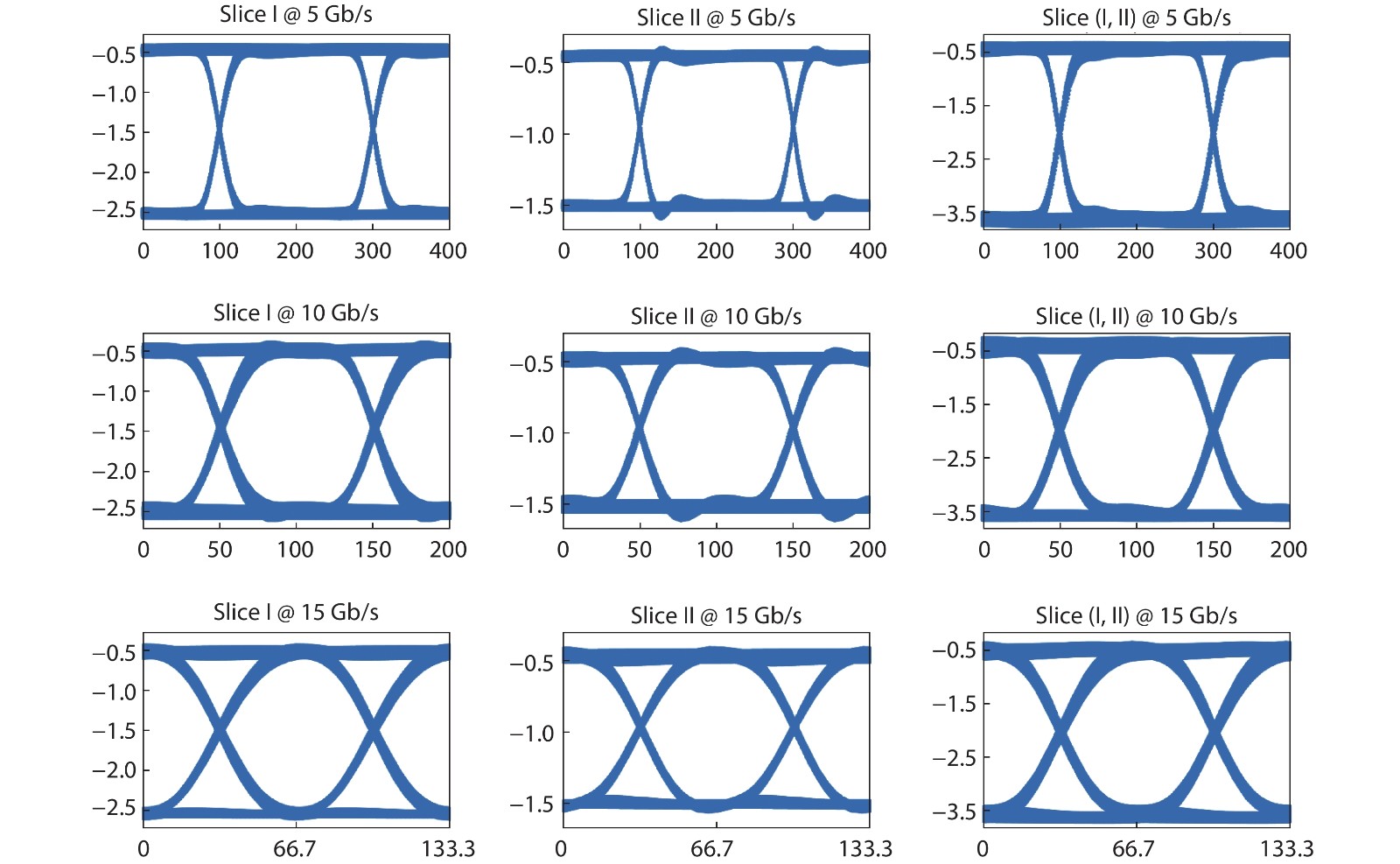
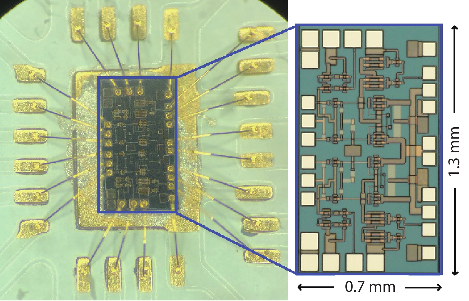
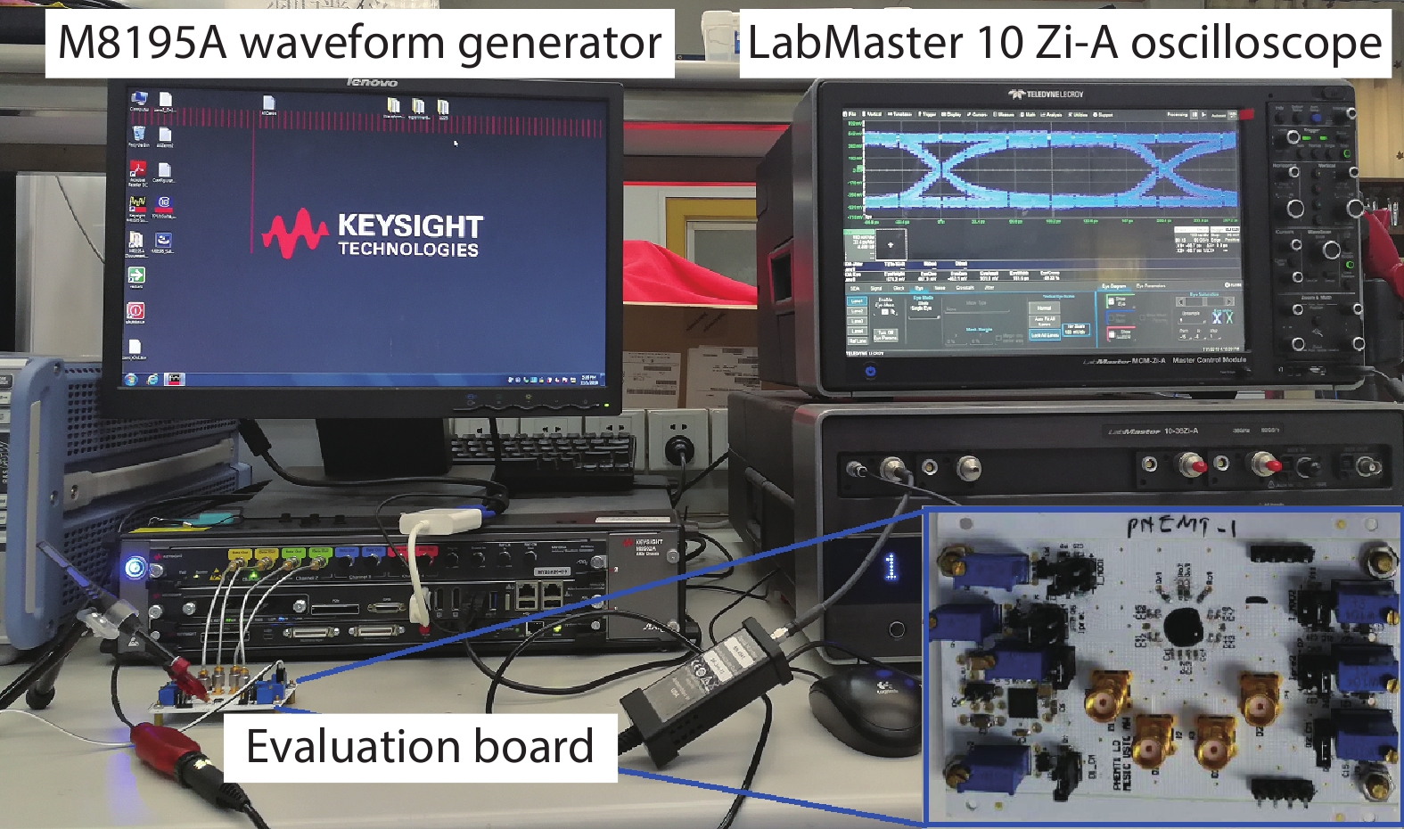
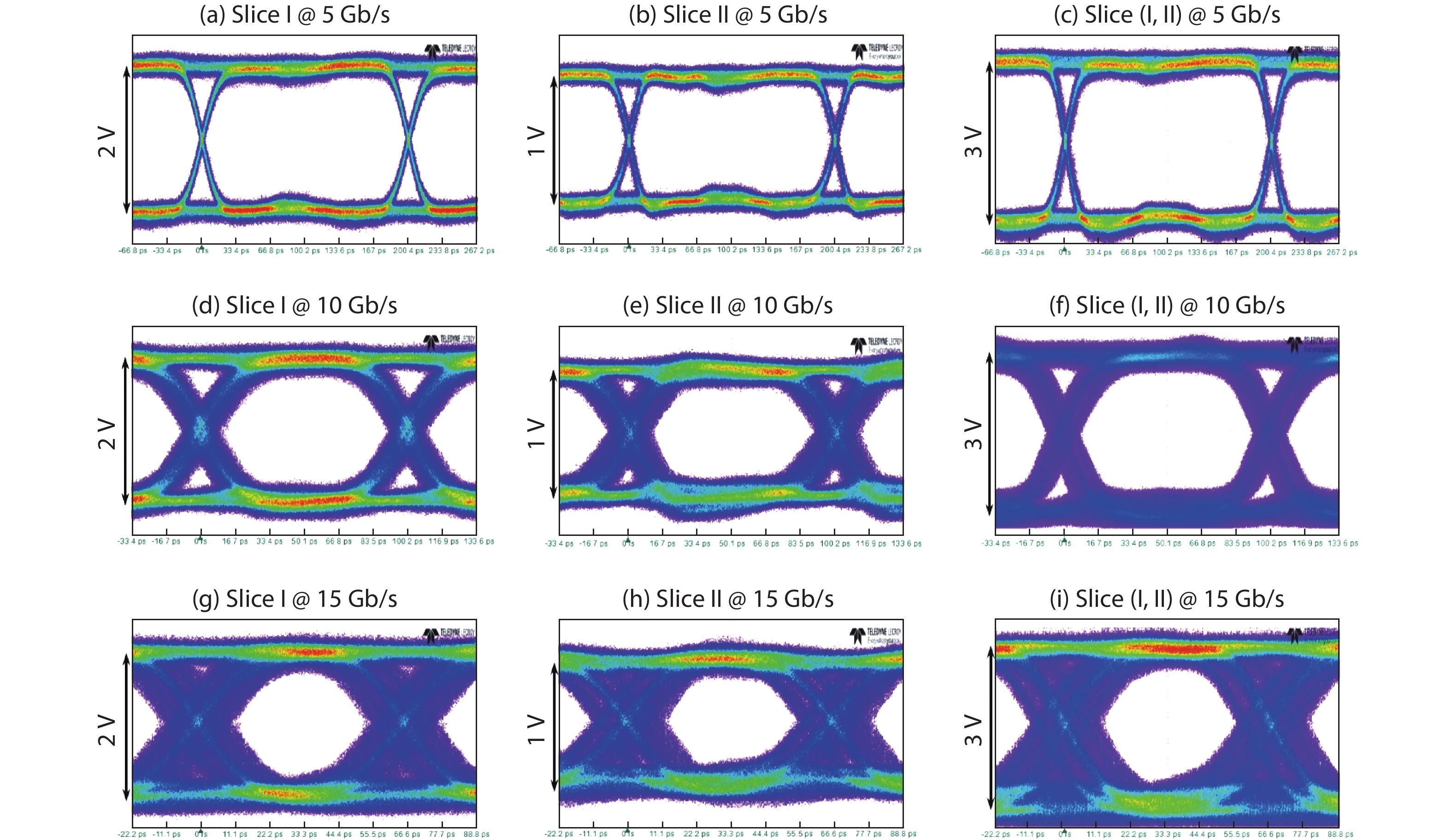
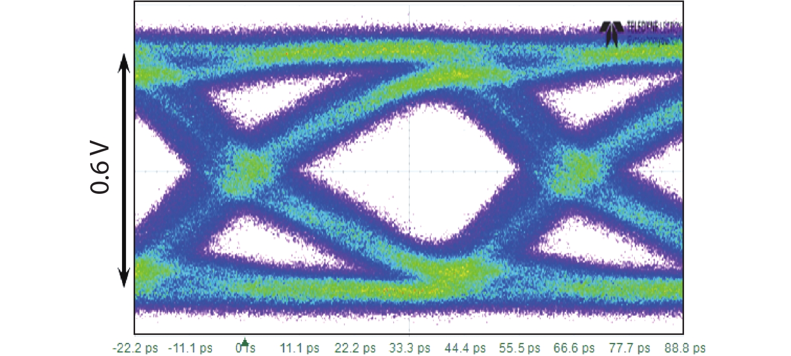
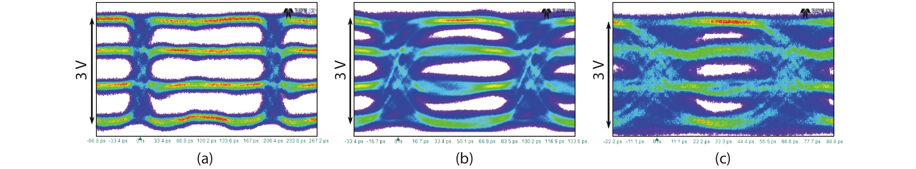
Table 1. Proposed driver performance at 15 Gbps when operated at different PVT corners.
| Parameter | Slice I | Slice II |
| Eye height (V) | 1.49–1.85 | 0.75–0.91 |
| Eye width (UI) | 0.82–0.9 | 0.84–0.91 |
| Rise time (ps) | 21.4–31 | 16.8–29.7 |
| Fall time (ps) | 19.7–30.5 | 16–29.1 |
| Total jitter (UI pk-pk) | 0.12–0.225 | 0.1–0.21 |
 DownLoad: CSV
Table 2. Performance summary and comparison to prior work.
| Parameter | This work | Ref. [9] | Ref. [4] | Ref. [7] | Ref. [2] | Ref. [10] | Ref. [21] | Ref. [11] | Ref. [30] | ||
| Modulation format | NRZ | PAM4 | NRZ | NRZ | NRZ | NRZ | NRZ | PAM4 | NRZ | PAM4 | NRZ |
| Data rate (Gbps) | 15 | 30 | 10 | 10 | 24 | 10.7 | 4.25 | 56 | 32 | 30 | 42 |
| Termination | Passive | Active | Passive | passive | Active | Active | Passive | Active | Passive | ||
| Output coupling | DC | DC | AC | DC | AC | DC | DC | DC | DC | ||
| Input swing (Vpp) (single-ended) | 0.3 | 0.4 | 0.4 | 0.5 | N/A | 0.2 | 0.15 | 0.15 | N/A | ||
| Modulation current (mA) | 120 | 100 | 100 | 56b | 80 | 80 | 6.4b | 44d | 32d | 6.6e | |
| Supply voltage (V) | –5.2 | –5.2 | 1.8/2 | –4.5 | 3.3 | 3.3 | 2.3/3 | 1.2/1.5 /3.3 | N/A | ||
| Power (W) | 1.228 | 1.3 | 0.675 | 1.8 | 0.67 | 0.343c | 0.115 | 0.55 | 0.0815 | ||
| Output return loss (dB) | < 10 dB up to13.2 GHza | < 10 dB up to12 GHz | N/A | N/A | < 10 dB up to10 GHz | N/A | < 8 dB up to30 GHz | N/A | N/A | ||
| FOM1 (A·Gbps/W) | 1.47 | 2.93 | 0.77 | 1.48 | 0.75 | 1.28 | 0.74 | 3.1 | 2.56 | 1.75 | 3.4 |
| FOM2 | 14.7% | 11.4% | 9.6% | 18.5% | 4.4% | 11.9% | 13.1% | 0.7% | 1.76% | 0.73% | 2.7% |
| Die area (mm2) | 0.91 | N/A | 1.62 | 1 | 2.25 | 2.66 | 0.59 | 1.2 | 0.5 | ||
| Technology | 0.15 µm GaAs E-mode pHEMT | 0.25 µm GaAs pHEMT | 0.18 µm CMOS | 0.2 µm GaAs pHEMT | SiGe SOI Bipolar | SiGe BiCMOS | SiGe BiCMOS | 65 nm CMOS | 14 nm Bulk CMOS | ||
| FOM1 is defined as the product of the modulation current and data rate divided by the power dissipation, without DC bias current of load devices.The higher, the better. FOM2 is the output power divided by the total power dissipation, without DC bias current of load devices. The higher the better. a Based on post-layout simulation results. b The modulation current is deduced from the measured eye diagram at 50-Ω output load. c Power and FOMs are given at 60 mA modulation current. d The modulation current is deduced from the measured eye diagram at 10-Ω equivalent output load. e Modulation current at 100-Ω load. | |||||||||||
DownLoad: CSV
| [1] |
Razavi B. Design of integrated circuits for optical communications. 2nd ed. Hoboken, New Jersey: WILEY, 2012
|
| [2] |
Morley S. A 3 V 10.7 Gb/s differential laser diode driver with active back-termination output stage. 2005 IEEE International Solid-State Circuits Conference, 2005, 220
|
| [3] |
Tsai C M, Chiu M C. A 10Gb/s laser-diode driver with active back-termination in 0.18 μm CMOS. 2008 IEEE International Solid-State Circuits Conference - Digest of Technical Papers, 2008, 222
|
| [4] |
Galal S, Razavi B. 10-Gb/s limiting amplifier and laser/modulator driver in 0.18-μm CMOS technology. IEEE J Solid-State Circuits, 2003, 38, 2138 doi: 10.1109/JSSC.2003.818567
|
| [5] |
Chiang P C, Jiang J Y, Hung H W, et al. 4 × 25 Gb/s transceiver with optical front-end for 100 GbE system in 65 nm CMOS technology. IEEE J Solid-State Circuits, 2015, 50, 573 doi: 10.1109/JSSC.2014.2365700
|
| [6] |
Takemoto T, Matsuoka Y, Sugiyama Y, et al. A 50-Gb/s NRZ-modulated optical transmitter based on a DFB-LD and a 0.18-μm SiGe BiCMOS LD driver. Optical Fiber Communication Conference, 2015, 1
|
| [7] |
Huang T, Wang Z G, Zhu E, et al. 24 Gb/s laser/modulator driver IC using 0.2 μm gate length PHEMTs. ESSCIRC 2004 - 29th European Solid-State Circuits Conference, 2003, 277
|
| [8] |
Takemoto T, Yamashita H, Yuki F, et al. A 25-Gb/s 2.2-W 65-nm CMOS optical transceiver using a power-supply-variation-tolerant analog front end and data-format conversion. IEEE J Solid-State Circuits, 2014, 49, 471 doi: 10.1109/JSSC.2013.2291099
|
| [9] |
Ransijn H, Salvador G, Daugherty D D, et al. A 10-Gb/s laser/modulator driver IC with a dual-mode actively matched output buffer. IEEE J Solid-State Circuits, 2001, 36, 1314 doi: 10.1109/4.944657
|
| [10] |
Fattaruso J W, Sheahan B. A 3-V 4.25-Gb/s laser driver with 0.4-V output voltage compliance. IEEE J Solid-State Circuits, 2006, 41, 1930 doi: 10.1109/JSSC.2006.875288
|
| [11] |
Yin B Z, Qi N, Shi J B, et al. A 32Gb/s-NRZ, 15GBaud/s-PAM4 DFB laser driver with active back-termination in 65 nm CMOS. 2017 IEEE Radio Frequency Integrated Circuits Symposium (RFIC), 2017, 264
|
| [12] |
Shi J B, Yin B Z, Qi N, et al. Design techniques for signal reflection suppression in high-speed 25-Gb/s laser drivers in CMOS. IEEE Photonics Technol Lett, 2018, 30, 39 doi: 10.1109/LPT.2017.2773525
|
| [13] |
Miyashita M, Yoshida N, Kojima Y, et al. An AlGaAs/InGaAs pseudomorphic HEMT modulator driver IC with low power dissipation for 10-Gb/s optical transmission systems. IEEE Trans Microw Theory Tech, 1997, 45, 1058 doi: 10.1109/22.598441
|
| [14] |
Bauwelinck J, Chen W, Verhulst D, et al. A high-resolution burst-mode laser transmitter with fast and accurate level monitoring for 1.25 Gb/s upstream GPONs. IEEE J Solid-State Circuits, 2005, 40, 1322 doi: 10.1109/JSSC.2005.848024
|
| [15] |
Umeda Y, Kanda A, Sano K, et al. 10 Gbit/s series-connected voltage-balancing pulse driver with high-speed input buffer. Electron Lett, 2004, 40, 934 doi: 10.1049/el:20045223
|
| [16] |
Chujo N, Takai T, Sugawara T, et al. A 25 Gb/s 65-nm CMOS low-power laser diode driver with mutually coupled peaking inductors for optical interconnects. IEEE Trans Circuits Syst I, 2011, 58, 2061 doi: 10.1109/TCSI.2011.2163982
|
| [17] |
Schow C L, Doany F E, Chen C, et al. Low-power 16 × 10 Gb/s Bi-directional single chip CMOS optical transceivers operating at < < 5 mW/Gb/s/link. IEEE J Solid-State Circuits, 2009, 44, 301 doi: 10.1109/JSSC.2008.2007439
|
| [18] |
Kromer C, Sialm G, Berger C, et al. A 100-mW 4 × 10 Gb/s transceiver in 80-nm CMOS for high-density optical interconnects. IEEE J Solid-State Circuits, 2005, 40, 2667 doi: 10.1109/JSSC.2005.856575
|
| [19] |
Wahba A, Li X, Xi N, et al. A 10 gb/s, 150 mA laser diode driver with active back-termination in 0.13-µm SOI CMOS technology. 2019 IEEE International Conference on Integrated Circuits, Technologies and Applications, 2019, 91
|
| [20] |
Belfiore G, Henker R, Ellinger F. 90 Gbit/s 4-level pulse-amplitude-modulation vertical-cavity surface-emitting laser driver integrated circuit in 130 nm SiGe technology. 2016 IEEE MTT-S Latin America Microwave Conference (LAMC), 2016, 1
|
| [21] |
Belfiore G, Szilagyi L, Henker R, et al. Design of a 56 Gbit/s 4-level pulse-amplitude-modulation inductor-less vertical-cavity surface-emitting laser driver integrated circuit in 130 nm BiCMOS technology. IET Circuits Devices Syst, 2015, 9, 213 doi: 10.1049/iet-cds.2014.0240
|
| [22] |
Belfiore G, Szilagyi L, Henker R, et al. Common cathode VCSEL driver in 90 nm CMOS enabling 25 Gbit/s optical connection using 14 Gbit/s 850 nm VCSEL. Electron Lett, 2015, 51, 349 doi: 10.1049/el.2014.4217
|
| [23] |
Gray P R, Hurst P J, Lewis S H, et al. Analysis and design of analog integrated circuits. John Wiley & Sons, 2009
|
| [24] |
Säckinger E. Broadband circuits for optical fiber communication. Hoboken, NJ, USA: John Wiley & Sons, Inc., 2005
|
| [25] |
Heydari P, Mohanavelu R. Design of ultrahigh-speed low-voltage CMOS CML buffers and latches. IEEE Trans Very Large Scale Integr VLSI Syst, 2004, 12, 1081 doi: 10.1109/TVLSI.2004.833663
|
| [26] |
Lao Z, Thiede A, Nowotny U, et al. High power modulator driver ICs up to 30 Gb/s with AlGaAs/GaAs HEMTs. IEEE Gallium Arsenide Integrated Circuit Symposium, 1997, 223
|
| [27] |
Zhu N H, Chen C, Pun E Y B, et al. Extraction of intrinsic response from S-parameters of laser diodes. IEEE Photonics Technol Lett, 2005, 17, 744 doi: 10.1109/LPT.2004.842794
|
| [28] |
Chen C, Zhu N, Zhang S, et al. Characterization of parasitics in TO-packaged high-speed laser modules. IEEE Trans Adv Packag, 2007, 30, 97 doi: 10.1109/TADVP.2006.884779
|
| [29] |
Gao J J. Optoelectronic integrated circuit design and device modeling. Chichester, UK: John Wiley & Sons, Ltd, 2010
|
| [30] |
Khafaji M, Pliva J, Henker R, et al. A 42-Gb/s VCSEL driver suitable for burst mode operation in 14-nm bulk CMOS. IEEE Photonics Technol Lett, 2018, 30, 23 doi: 10.1109/LPT.2017.2771952
|


Article views: 3683 Times PDF downloads: 191 Times Cited by: 0 Times
Received: 13 December 2020 Revised: 11 February 2021 Online: Accepted Manuscript: 08 April 2021Uncorrected proof: 08 April 2021Published: 05 July 2021
| Citation: |
Ahmed Wahba, Lin Cheng, Fujiang Lin. A 15 Gbps-NRZ, 30 Gbps-PAM4, 120 mA laser diode driver implemented in 0.15-µm GaAs E-mode pHEMT technology[J]. Journal of Semiconductors, 2021, 42(7): 072401. doi: 10.1088/1674-4926/42/7/072401
A Wahba, L Cheng, F Lin, A 15 Gbps-NRZ, 30 Gbps-PAM4, 120 mA laser diode driver implemented in 0.15-µm GaAs E-mode pHEMT technology[J]. J. Semicond., 2021, 42(7): 072401. doi: 10.1088/1674-4926/42/7/072401.
Export: BibTex EndNote

|
| [1] |
Razavi B. Design of integrated circuits for optical communications. 2nd ed. Hoboken, New Jersey: WILEY, 2012
|
| [2] |
Morley S. A 3 V 10.7 Gb/s differential laser diode driver with active back-termination output stage. 2005 IEEE International Solid-State Circuits Conference, 2005, 220
|
| [3] |
Tsai C M, Chiu M C. A 10Gb/s laser-diode driver with active back-termination in 0.18 μm CMOS. 2008 IEEE International Solid-State Circuits Conference - Digest of Technical Papers, 2008, 222
|
| [4] |
Galal S, Razavi B. 10-Gb/s limiting amplifier and laser/modulator driver in 0.18-μm CMOS technology. IEEE J Solid-State Circuits, 2003, 38, 2138 doi: 10.1109/JSSC.2003.818567
|
| [5] |
Chiang P C, Jiang J Y, Hung H W, et al. 4 × 25 Gb/s transceiver with optical front-end for 100 GbE system in 65 nm CMOS technology. IEEE J Solid-State Circuits, 2015, 50, 573 doi: 10.1109/JSSC.2014.2365700
|
| [6] |
Takemoto T, Matsuoka Y, Sugiyama Y, et al. A 50-Gb/s NRZ-modulated optical transmitter based on a DFB-LD and a 0.18-μm SiGe BiCMOS LD driver. Optical Fiber Communication Conference, 2015, 1
|
| [7] |
Huang T, Wang Z G, Zhu E, et al. 24 Gb/s laser/modulator driver IC using 0.2 μm gate length PHEMTs. ESSCIRC 2004 - 29th European Solid-State Circuits Conference, 2003, 277
|
| [8] |
Takemoto T, Yamashita H, Yuki F, et al. A 25-Gb/s 2.2-W 65-nm CMOS optical transceiver using a power-supply-variation-tolerant analog front end and data-format conversion. IEEE J Solid-State Circuits, 2014, 49, 471 doi: 10.1109/JSSC.2013.2291099
|
| [9] |
Ransijn H, Salvador G, Daugherty D D, et al. A 10-Gb/s laser/modulator driver IC with a dual-mode actively matched output buffer. IEEE J Solid-State Circuits, 2001, 36, 1314 doi: 10.1109/4.944657
|
| [10] |
Fattaruso J W, Sheahan B. A 3-V 4.25-Gb/s laser driver with 0.4-V output voltage compliance. IEEE J Solid-State Circuits, 2006, 41, 1930 doi: 10.1109/JSSC.2006.875288
|
| [11] |
Yin B Z, Qi N, Shi J B, et al. A 32Gb/s-NRZ, 15GBaud/s-PAM4 DFB laser driver with active back-termination in 65 nm CMOS. 2017 IEEE Radio Frequency Integrated Circuits Symposium (RFIC), 2017, 264
|
| [12] |
Shi J B, Yin B Z, Qi N, et al. Design techniques for signal reflection suppression in high-speed 25-Gb/s laser drivers in CMOS. IEEE Photonics Technol Lett, 2018, 30, 39 doi: 10.1109/LPT.2017.2773525
|
| [13] |
Miyashita M, Yoshida N, Kojima Y, et al. An AlGaAs/InGaAs pseudomorphic HEMT modulator driver IC with low power dissipation for 10-Gb/s optical transmission systems. IEEE Trans Microw Theory Tech, 1997, 45, 1058 doi: 10.1109/22.598441
|
| [14] |
Bauwelinck J, Chen W, Verhulst D, et al. A high-resolution burst-mode laser transmitter with fast and accurate level monitoring for 1.25 Gb/s upstream GPONs. IEEE J Solid-State Circuits, 2005, 40, 1322 doi: 10.1109/JSSC.2005.848024
|
| [15] |
Umeda Y, Kanda A, Sano K, et al. 10 Gbit/s series-connected voltage-balancing pulse driver with high-speed input buffer. Electron Lett, 2004, 40, 934 doi: 10.1049/el:20045223
|
| [16] |
Chujo N, Takai T, Sugawara T, et al. A 25 Gb/s 65-nm CMOS low-power laser diode driver with mutually coupled peaking inductors for optical interconnects. IEEE Trans Circuits Syst I, 2011, 58, 2061 doi: 10.1109/TCSI.2011.2163982
|
| [17] |
Schow C L, Doany F E, Chen C, et al. Low-power 16 × 10 Gb/s Bi-directional single chip CMOS optical transceivers operating at < < 5 mW/Gb/s/link. IEEE J Solid-State Circuits, 2009, 44, 301 doi: 10.1109/JSSC.2008.2007439
|
| [18] |
Kromer C, Sialm G, Berger C, et al. A 100-mW 4 × 10 Gb/s transceiver in 80-nm CMOS for high-density optical interconnects. IEEE J Solid-State Circuits, 2005, 40, 2667 doi: 10.1109/JSSC.2005.856575
|
| [19] |
Wahba A, Li X, Xi N, et al. A 10 gb/s, 150 mA laser diode driver with active back-termination in 0.13-µm SOI CMOS technology. 2019 IEEE International Conference on Integrated Circuits, Technologies and Applications, 2019, 91
|
| [20] |
Belfiore G, Henker R, Ellinger F. 90 Gbit/s 4-level pulse-amplitude-modulation vertical-cavity surface-emitting laser driver integrated circuit in 130 nm SiGe technology. 2016 IEEE MTT-S Latin America Microwave Conference (LAMC), 2016, 1
|
| [21] |
Belfiore G, Szilagyi L, Henker R, et al. Design of a 56 Gbit/s 4-level pulse-amplitude-modulation inductor-less vertical-cavity surface-emitting laser driver integrated circuit in 130 nm BiCMOS technology. IET Circuits Devices Syst, 2015, 9, 213 doi: 10.1049/iet-cds.2014.0240
|
| [22] |
Belfiore G, Szilagyi L, Henker R, et al. Common cathode VCSEL driver in 90 nm CMOS enabling 25 Gbit/s optical connection using 14 Gbit/s 850 nm VCSEL. Electron Lett, 2015, 51, 349 doi: 10.1049/el.2014.4217
|
| [23] |
Gray P R, Hurst P J, Lewis S H, et al. Analysis and design of analog integrated circuits. John Wiley & Sons, 2009
|
| [24] |
Säckinger E. Broadband circuits for optical fiber communication. Hoboken, NJ, USA: John Wiley & Sons, Inc., 2005
|
| [25] |
Heydari P, Mohanavelu R. Design of ultrahigh-speed low-voltage CMOS CML buffers and latches. IEEE Trans Very Large Scale Integr VLSI Syst, 2004, 12, 1081 doi: 10.1109/TVLSI.2004.833663
|
| [26] |
Lao Z, Thiede A, Nowotny U, et al. High power modulator driver ICs up to 30 Gb/s with AlGaAs/GaAs HEMTs. IEEE Gallium Arsenide Integrated Circuit Symposium, 1997, 223
|
| [27] |
Zhu N H, Chen C, Pun E Y B, et al. Extraction of intrinsic response from S-parameters of laser diodes. IEEE Photonics Technol Lett, 2005, 17, 744 doi: 10.1109/LPT.2004.842794
|
| [28] |
Chen C, Zhu N, Zhang S, et al. Characterization of parasitics in TO-packaged high-speed laser modules. IEEE Trans Adv Packag, 2007, 30, 97 doi: 10.1109/TADVP.2006.884779
|
| [29] |
Gao J J. Optoelectronic integrated circuit design and device modeling. Chichester, UK: John Wiley & Sons, Ltd, 2010
|
| [30] |
Khafaji M, Pliva J, Henker R, et al. A 42-Gb/s VCSEL driver suitable for burst mode operation in 14-nm bulk CMOS. IEEE Photonics Technol Lett, 2018, 30, 23 doi: 10.1109/LPT.2017.2771952
|

 WeChat ID
Journal of Semiconductors © 2017 All Rights Reserved 京ICP备05085259号-2