


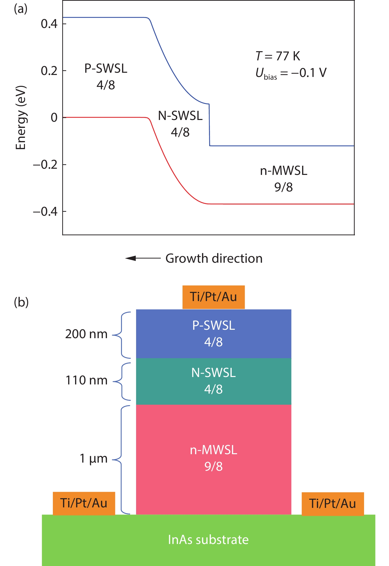
Fig. 1.
(Color online) (a) Energy-band diagram of the PNn device at 77 K. (b) Cross-section of the PNn detector, where 4/8 and 9/8 stand for 4 monolayer InAs/8 monolayer GaSb and 9 monolayer InAs/8 monolayer GaSb, respectively.
ARTICLES
Xiujun Hao1, 2, Yan Teng1, He Zhu1, Jiafeng Liu1, Hong Zhu1, Yunlong Huai1, Meng Li1, 2, Baile Chen3, Yong Huang1, and Hui Yang1, 2
Corresponding author: Yong Huang, yhuang2014@sinano.ac.cn
Abstract: We demonstrate a high-operating-temperature (HOT) mid-wavelength InAs/GaSb superlattice heterojunction infrared photodetector grown by metal–organic chemical vapor deposition. High crystalline quality and the near-zero lattice mismatch of a InAs/GaSb superlattice on an InAs substrate were evidenced by high-resolution X-ray diffraction. At a bias voltage of –0.1 V and an operating temperature of 200 K, the device exhibited a 50% cutoff wavelength of ~ 4.9 μm, a dark current density of 0.012 A/cm2, and a peak specific detectivity of 2.3 × 109 cm·Hz1/2 /W.
Key words: HOT, MWIR, InAs/GaSb superlattice, aluminum-free, MOCVD
| [1] |
Martyniuk P, Rogalski A. HOT infrared photodetectors. Opto Electron Rev, 2013, 21, 239 doi: 10.2478/s11772−013−0090−x
|
| [2] |
Markovitz T, Pivnik I, Calahorra Z, et al. Digital 640x512/15μm InSb detector for high frame rate, high sensitivity, and low power applications. Infrared Technology and Applications XXXVII, 2011, 8012, 80122Y doi: 10.1117/12.883345
|
| [3] |
Klipstein P, Aronov D, Ezra M B, et al. Recent progress in InSb based quantum detectors in Israel. Infrared Phys Technol, 2013, 59, 172 doi: 10.1016/j.infrared.2012.12.035
|
| [4] |
Jóźwikowski K, Kopytko M, Piotrowski J, et al. Near-room temperature MWIR HgCdTe photodiodes limited by vacancies and dislocations related to Shockley-Read-Hall centres. Solid State Electron, 2011, 63, 8 doi: 10.1016/j.sse.2011.05.030
|
| [5] |
Smith D L, Mailhiot C. Proposal for strained type II superlattice infrared detectors. J Appl Phys, 1987, 62, 2545 doi: 10.1063/1.339468
|
| [6] |
Grein C H, Young P M, Flatté M E, et al. Long wavelength InAs/InGaSb infrared detectors: Optimization of carrier lifetimes. J Appl Phys, 1995, 78, 7143 doi: 10.1063/1.360422
|
| [7] |
Nguyen B M, Chen G X, Hoang M A, et al. Growth and characterization of long-wavelength infrared type-II superlattice photodiodes on a 3-in GaSb wafer. IEEE J Quantum Electron, 2011, 47, 686 doi: 10.1109/JQE.2010.2103049
|
| [8] |
Razeghi M, Abdollahi Pour S, Huang E K, et al. Type-II InAs/GaSb photodiodes and focal plane arrays aimed at high operating temperatures. Opto Electron Rev, 2011, 19, 261 doi: 10.2478/s11772-011-0028-0
|
| [9] |
Höglund L, Asplund C, Marcks von Würtemberg R, et al. Manufacturability of type-II InAs/GaSb superlattice detectors for infrared imaging. Infrared Phys Technol, 2017, 84, 28 doi: 10.1016/j.infrared.2017.03.002
|
| [10] |
Sun Y Y, Wang G W, Han X, et al. 320 × 256 high operating temperature mid-infrared focal plane arrays based on type-II InAs/GaSb superlattice. Superlattices Microstruct, 2017, 111, 783 doi: 10.1016/j.spmi.2017.07.037
|
| [11] |
Gautam N, Myers S, Barve A V, et al. Band engineered HOT midwave infrared detectors based on type-II InAs/GaSb strained layer superlattices. Infrared Phys Technol, 2013, 59, 72 doi: 10.1016/j.infrared.2012.12.017
|
| [12] |
Teng Y, Zhao Y, Wu Q H, et al. High-performance long-wavelength InAs/GaSb superlattice detectors grown by MOCVD. IEEE Photonics Technol Lett, 2019, 31, 185 doi: 10.1109/LPT.2018.2889575
|
| [13] |
Zhao Y, Teng Y, Hao X J, et al. Optimization of long-wavelength InAs/GaSb superlattice photodiodes with Al-free barriers. IEEE Photonics Technol Lett, 2020, 32, 19 doi: 10.1109/LPT.2019.2955562
|
| [14] |
Ting D Z Y, Soibel A, Höglund L, et al. Type-II superlattice infrared detectors. In: Advances in Infrared Photodetectors. Amsterdam: Elsevier, 2011
|
| [15] |
Li X, Zhao Y, Wu Q H, et al. Exploring the optimum growth conditions for InAs/GaSb and GaAs/GaSb superlattices on InAs substrates by metalorganic chemical vapor deposition. J Cryst Growth, 2018, 502, 71 doi: 10.1016/j.jcrysgro.2018.09.003
|
| [16] |
Soibel A, Keo S A, Fisher A, et al. High operating temperature nBn detector with monolithically integrated microlens. Appl Phys Lett, 2018, 112, 041105 doi: 10.1063/1.5011348
|
| [17] |
Ting D Z Y, Hill C J, Soibel A, et al. A high-performance long wavelength superlattice complementary barrier infrared detector. Appl Phys Lett, 2009, 95, 023508 doi: 10.1063/1.3177333
|
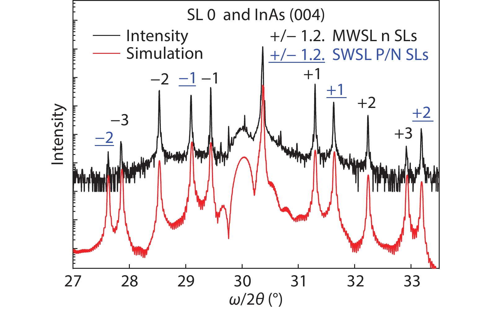
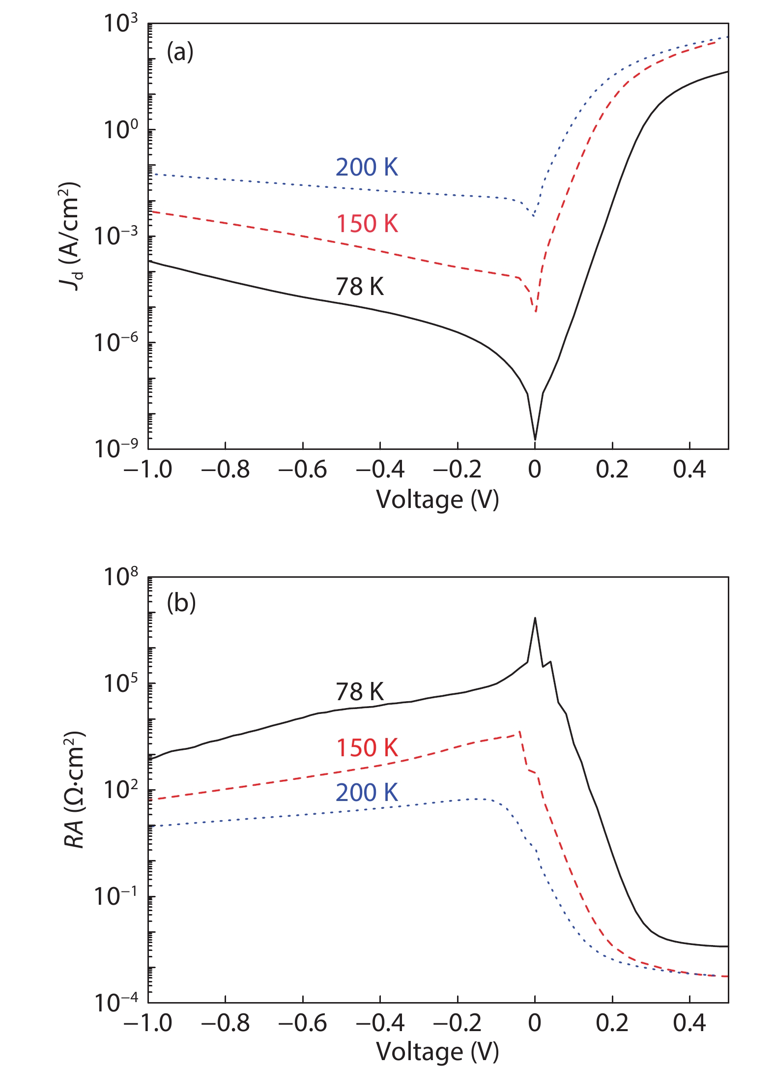
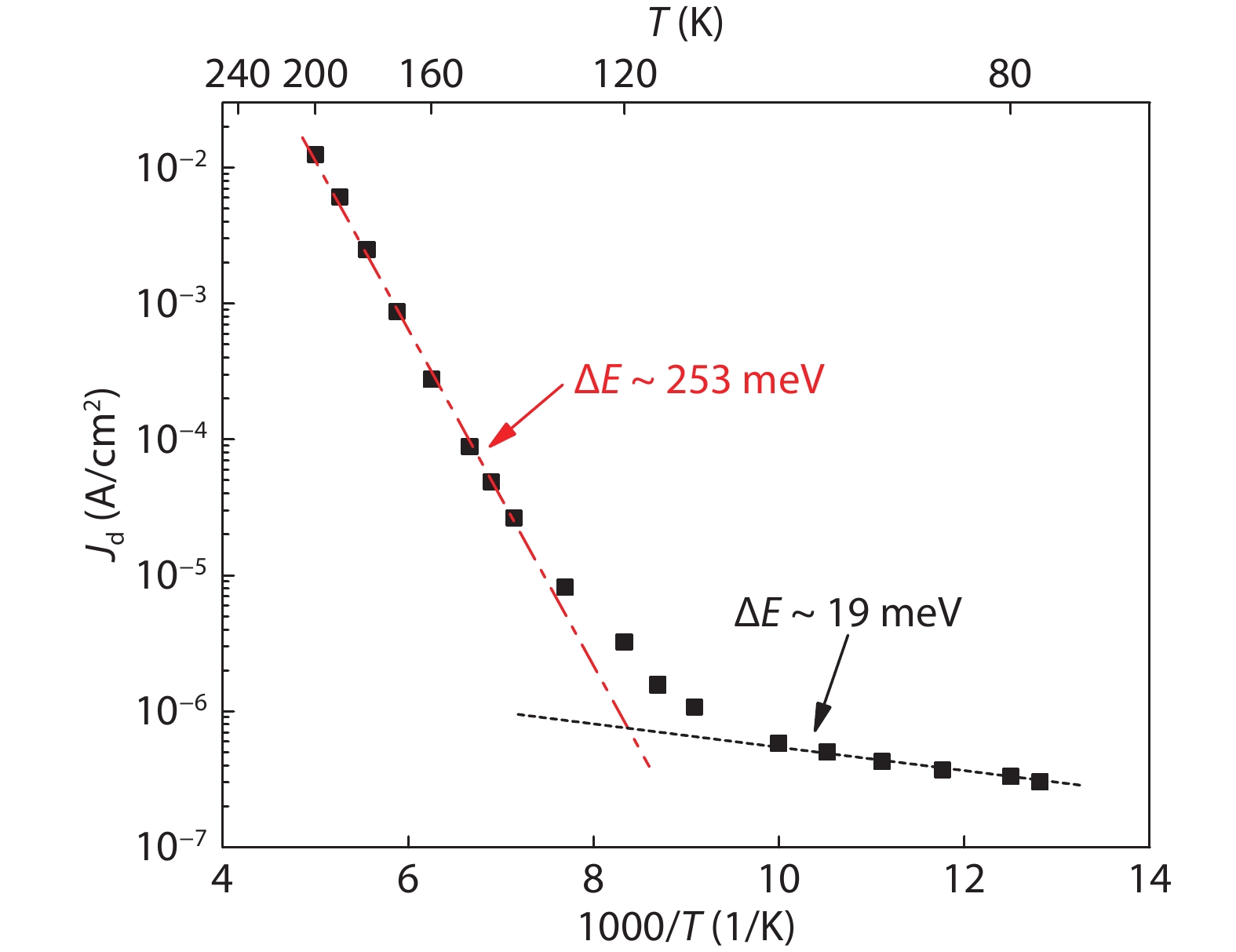

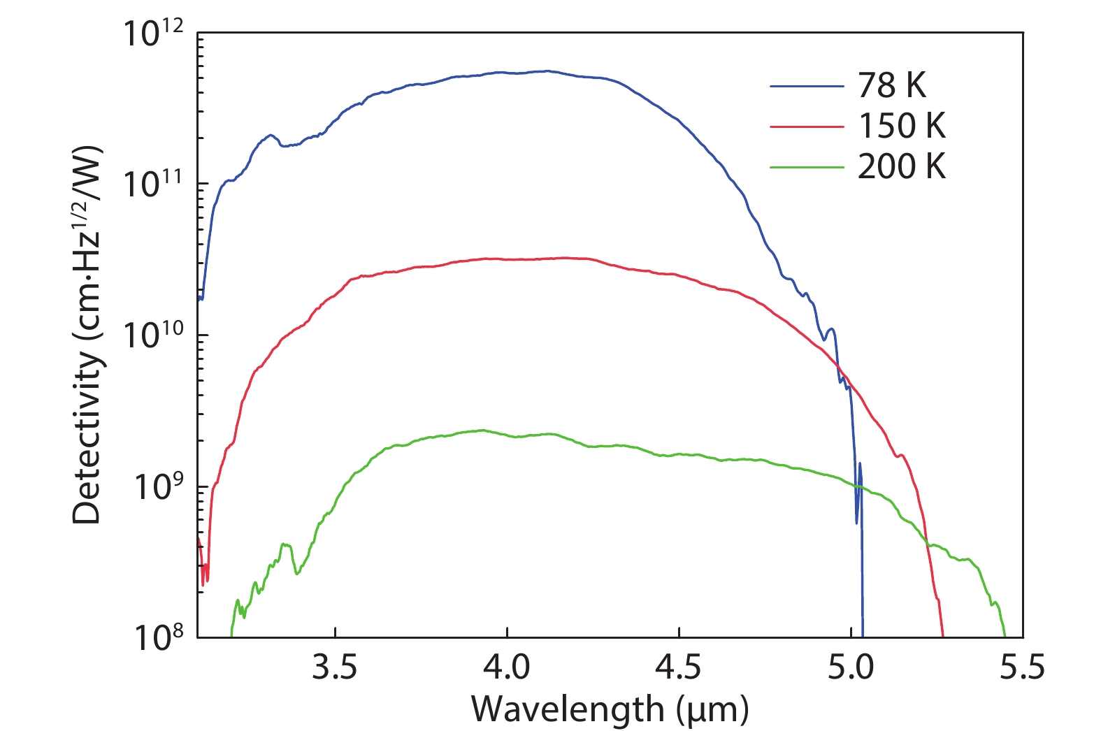
Table 1. 50% cutoff wavelengths at 78, 150, and 200 K.
| Temperature (K) | 78 | 150 | 200 |
| λ50% cutoff (μm) | 4.5 | 4.7 | 4.9 |
 DownLoad: CSV
| [1] |
Martyniuk P, Rogalski A. HOT infrared photodetectors. Opto Electron Rev, 2013, 21, 239 doi: 10.2478/s11772−013−0090−x
|
| [2] |
Markovitz T, Pivnik I, Calahorra Z, et al. Digital 640x512/15μm InSb detector for high frame rate, high sensitivity, and low power applications. Infrared Technology and Applications XXXVII, 2011, 8012, 80122Y doi: 10.1117/12.883345
|
| [3] |
Klipstein P, Aronov D, Ezra M B, et al. Recent progress in InSb based quantum detectors in Israel. Infrared Phys Technol, 2013, 59, 172 doi: 10.1016/j.infrared.2012.12.035
|
| [4] |
Jóźwikowski K, Kopytko M, Piotrowski J, et al. Near-room temperature MWIR HgCdTe photodiodes limited by vacancies and dislocations related to Shockley-Read-Hall centres. Solid State Electron, 2011, 63, 8 doi: 10.1016/j.sse.2011.05.030
|
| [5] |
Smith D L, Mailhiot C. Proposal for strained type II superlattice infrared detectors. J Appl Phys, 1987, 62, 2545 doi: 10.1063/1.339468
|
| [6] |
Grein C H, Young P M, Flatté M E, et al. Long wavelength InAs/InGaSb infrared detectors: Optimization of carrier lifetimes. J Appl Phys, 1995, 78, 7143 doi: 10.1063/1.360422
|
| [7] |
Nguyen B M, Chen G X, Hoang M A, et al. Growth and characterization of long-wavelength infrared type-II superlattice photodiodes on a 3-in GaSb wafer. IEEE J Quantum Electron, 2011, 47, 686 doi: 10.1109/JQE.2010.2103049
|
| [8] |
Razeghi M, Abdollahi Pour S, Huang E K, et al. Type-II InAs/GaSb photodiodes and focal plane arrays aimed at high operating temperatures. Opto Electron Rev, 2011, 19, 261 doi: 10.2478/s11772-011-0028-0
|
| [9] |
Höglund L, Asplund C, Marcks von Würtemberg R, et al. Manufacturability of type-II InAs/GaSb superlattice detectors for infrared imaging. Infrared Phys Technol, 2017, 84, 28 doi: 10.1016/j.infrared.2017.03.002
|
| [10] |
Sun Y Y, Wang G W, Han X, et al. 320 × 256 high operating temperature mid-infrared focal plane arrays based on type-II InAs/GaSb superlattice. Superlattices Microstruct, 2017, 111, 783 doi: 10.1016/j.spmi.2017.07.037
|
| [11] |
Gautam N, Myers S, Barve A V, et al. Band engineered HOT midwave infrared detectors based on type-II InAs/GaSb strained layer superlattices. Infrared Phys Technol, 2013, 59, 72 doi: 10.1016/j.infrared.2012.12.017
|
| [12] |
Teng Y, Zhao Y, Wu Q H, et al. High-performance long-wavelength InAs/GaSb superlattice detectors grown by MOCVD. IEEE Photonics Technol Lett, 2019, 31, 185 doi: 10.1109/LPT.2018.2889575
|
| [13] |
Zhao Y, Teng Y, Hao X J, et al. Optimization of long-wavelength InAs/GaSb superlattice photodiodes with Al-free barriers. IEEE Photonics Technol Lett, 2020, 32, 19 doi: 10.1109/LPT.2019.2955562
|
| [14] |
Ting D Z Y, Soibel A, Höglund L, et al. Type-II superlattice infrared detectors. In: Advances in Infrared Photodetectors. Amsterdam: Elsevier, 2011
|
| [15] |
Li X, Zhao Y, Wu Q H, et al. Exploring the optimum growth conditions for InAs/GaSb and GaAs/GaSb superlattices on InAs substrates by metalorganic chemical vapor deposition. J Cryst Growth, 2018, 502, 71 doi: 10.1016/j.jcrysgro.2018.09.003
|
| [16] |
Soibel A, Keo S A, Fisher A, et al. High operating temperature nBn detector with monolithically integrated microlens. Appl Phys Lett, 2018, 112, 041105 doi: 10.1063/1.5011348
|
| [17] |
Ting D Z Y, Hill C J, Soibel A, et al. A high-performance long wavelength superlattice complementary barrier infrared detector. Appl Phys Lett, 2009, 95, 023508 doi: 10.1063/1.3177333
|


Article views: 2046 Times PDF downloads: 89 Times Cited by: 0 Times
Received: 31 May 2021 Revised: 19 June 2021 Online: Accepted Manuscript: 04 August 2021Uncorrected proof: 16 August 2021Published: 04 January 2022
| Citation: |
Xiujun Hao, Yan Teng, He Zhu, Jiafeng Liu, Hong Zhu, Yunlong Huai, Meng Li, Baile Chen, Yong Huang, Hui Yang. High-operating-temperature MWIR photodetector based on a InAs/GaSb superlattice grown by MOCVD[J]. Journal of Semiconductors, 2022, 43(1): 012303. doi: 10.1088/1674-4926/43/1/012303
X J Hao, Y Teng, H Zhu, J F Liu, H Zhu, Y L Huai, M Li, B L Chen, Y Huang, H Yang, High-operating-temperature MWIR photodetector based on a InAs/GaSb superlattice grown by MOCVD[J]. J. Semicond., 2022, 43(1): 012303. doi: 10.1088/1674-4926/43/1/012303.
Export: BibTex EndNote

|
| [1] |
Martyniuk P, Rogalski A. HOT infrared photodetectors. Opto Electron Rev, 2013, 21, 239 doi: 10.2478/s11772−013−0090−x
|
| [2] |
Markovitz T, Pivnik I, Calahorra Z, et al. Digital 640x512/15μm InSb detector for high frame rate, high sensitivity, and low power applications. Infrared Technology and Applications XXXVII, 2011, 8012, 80122Y doi: 10.1117/12.883345
|
| [3] |
Klipstein P, Aronov D, Ezra M B, et al. Recent progress in InSb based quantum detectors in Israel. Infrared Phys Technol, 2013, 59, 172 doi: 10.1016/j.infrared.2012.12.035
|
| [4] |
Jóźwikowski K, Kopytko M, Piotrowski J, et al. Near-room temperature MWIR HgCdTe photodiodes limited by vacancies and dislocations related to Shockley-Read-Hall centres. Solid State Electron, 2011, 63, 8 doi: 10.1016/j.sse.2011.05.030
|
| [5] |
Smith D L, Mailhiot C. Proposal for strained type II superlattice infrared detectors. J Appl Phys, 1987, 62, 2545 doi: 10.1063/1.339468
|
| [6] |
Grein C H, Young P M, Flatté M E, et al. Long wavelength InAs/InGaSb infrared detectors: Optimization of carrier lifetimes. J Appl Phys, 1995, 78, 7143 doi: 10.1063/1.360422
|
| [7] |
Nguyen B M, Chen G X, Hoang M A, et al. Growth and characterization of long-wavelength infrared type-II superlattice photodiodes on a 3-in GaSb wafer. IEEE J Quantum Electron, 2011, 47, 686 doi: 10.1109/JQE.2010.2103049
|
| [8] |
Razeghi M, Abdollahi Pour S, Huang E K, et al. Type-II InAs/GaSb photodiodes and focal plane arrays aimed at high operating temperatures. Opto Electron Rev, 2011, 19, 261 doi: 10.2478/s11772-011-0028-0
|
| [9] |
Höglund L, Asplund C, Marcks von Würtemberg R, et al. Manufacturability of type-II InAs/GaSb superlattice detectors for infrared imaging. Infrared Phys Technol, 2017, 84, 28 doi: 10.1016/j.infrared.2017.03.002
|
| [10] |
Sun Y Y, Wang G W, Han X, et al. 320 × 256 high operating temperature mid-infrared focal plane arrays based on type-II InAs/GaSb superlattice. Superlattices Microstruct, 2017, 111, 783 doi: 10.1016/j.spmi.2017.07.037
|
| [11] |
Gautam N, Myers S, Barve A V, et al. Band engineered HOT midwave infrared detectors based on type-II InAs/GaSb strained layer superlattices. Infrared Phys Technol, 2013, 59, 72 doi: 10.1016/j.infrared.2012.12.017
|
| [12] |
Teng Y, Zhao Y, Wu Q H, et al. High-performance long-wavelength InAs/GaSb superlattice detectors grown by MOCVD. IEEE Photonics Technol Lett, 2019, 31, 185 doi: 10.1109/LPT.2018.2889575
|
| [13] |
Zhao Y, Teng Y, Hao X J, et al. Optimization of long-wavelength InAs/GaSb superlattice photodiodes with Al-free barriers. IEEE Photonics Technol Lett, 2020, 32, 19 doi: 10.1109/LPT.2019.2955562
|
| [14] |
Ting D Z Y, Soibel A, Höglund L, et al. Type-II superlattice infrared detectors. In: Advances in Infrared Photodetectors. Amsterdam: Elsevier, 2011
|
| [15] |
Li X, Zhao Y, Wu Q H, et al. Exploring the optimum growth conditions for InAs/GaSb and GaAs/GaSb superlattices on InAs substrates by metalorganic chemical vapor deposition. J Cryst Growth, 2018, 502, 71 doi: 10.1016/j.jcrysgro.2018.09.003
|
| [16] |
Soibel A, Keo S A, Fisher A, et al. High operating temperature nBn detector with monolithically integrated microlens. Appl Phys Lett, 2018, 112, 041105 doi: 10.1063/1.5011348
|
| [17] |
Ting D Z Y, Hill C J, Soibel A, et al. A high-performance long wavelength superlattice complementary barrier infrared detector. Appl Phys Lett, 2009, 95, 023508 doi: 10.1063/1.3177333
|

 WeChat ID
Journal of Semiconductors © 2017 All Rights Reserved 京ICP备05085259号-2


