


Fig. 1.
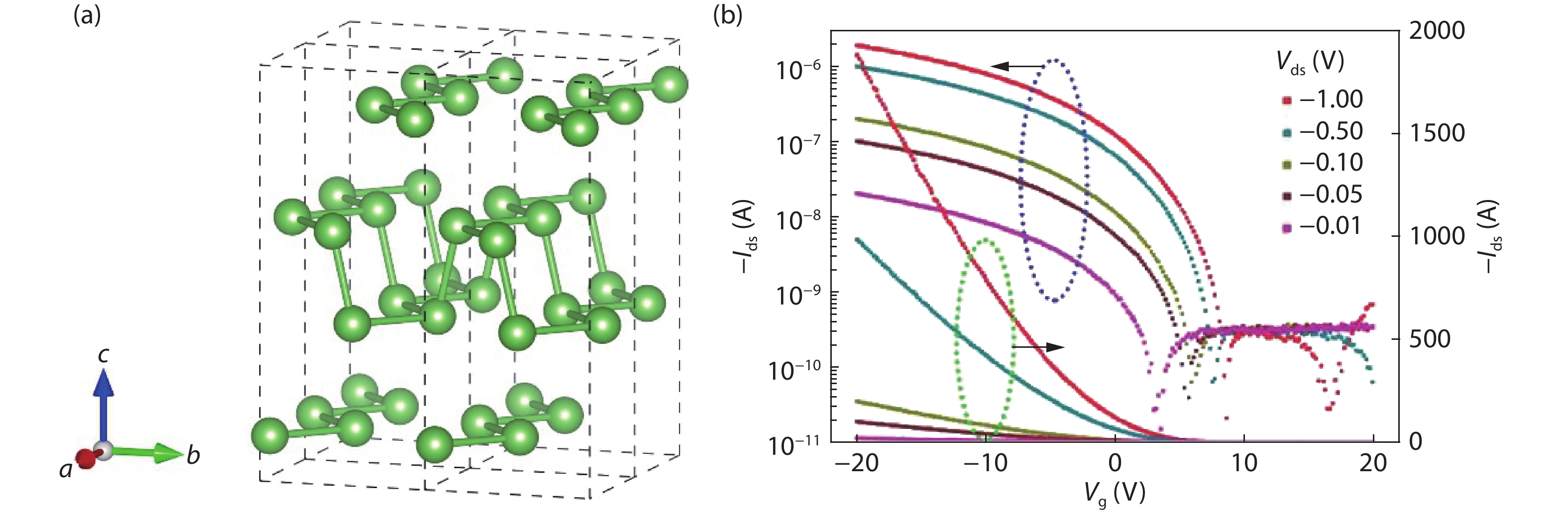
(Color online) (a) 3D crystal structures of b-As. (b) Transfer characteristics (Ids–Vg) of the monolayer b-As FET[5]. Copyright 2018 John Wiley and Sons.
NEWS AND VIEWS
Mianzeng Zhong and Jun He
Corresponding author: Jun He, E-mail: junhe@csu.edu.cn
| [1] |
Schwierz F. Graphene transistors. Nat Nanotechnol, 2010, 5, 487 doi: 10.1038/nnano.2010.89
|
| [2] |
Li L, Yu Y, Ye G J, et al. Black phosphorus field-effect transistors. Nat Nanotechnol, 2014, 9, 372 doi: 10.1038/nnano.2014.35
|
| [3] |
Island J O, Steele G A, van der Zant H S, et al. Environmental instability of few-layer black phosphorus. 2D Mater, 2015, 2, 011002 doi: 10.1088/2053-1583/2/1/011002
|
| [4] |
Chen Y, Chen C, Kealhofer R, et al. Black arsenic: a layered semiconductor with extreme in-plane anisotropy. Adv Mater, 2018, 30, 1800754 doi: 10.1002/adma.201800754
|
| [5] |
Zhong M, Xia Q, Pan L, et al. Thickness-dependent carrier transport characteristics of a new 2D elemental semiconductor: black arsenic. Adv Funct Mater, 2018, 28, 1802581 doi: 10.1002/adfm.201802581
|
| [6] |
Zhang S, Yan Z, Li Y, et al. Atomically thin arsenene and antimonene: semimetal–semiconductor and indirect–direct band-gap transitions. Angew Chem Int Ed, 2015, 54, 3112 doi: 10.1002/anie.201411246
|
| [7] |
Kou L, Ma Y, Tan X, et al. Structural and electronic properties of layered arsenic and antimony arsenide. J Phys Chem C, 2015, 119, 6918 doi: 10.1021/acs.jpcc.5b02096
|
| [8] |
Kamal C, Ezawa M. Arsenene: Two-dimensional buckled and puckered honeycomb arsenic systems. Phys Rev B, 2015, 91, 085423 doi: 10.1103/PhysRevB.91.085423
|
| [9] |
Luo K, Chen S, Duan C. Indirect-direct band gap transition of two-dimensional arsenic layered semiconductors — cousins of black phosphorus. Sci China Phys, Mechan Astron, 2015, 58, 1 doi: 10.1007/s11433-015-5665-8
|
| [10] |
Wang C, Xia Q, Nie Y, et al. Strain engineering band gap, effective mass and anisotropic Dirac-like cone in monolayer arsenene. AIP Adv, 2016, 6, 035204 doi: 10.1063/1.4943548
|
| [11] |
Zhang Z, Xie J, Yang D, et al. Manifestation of unexpected semiconducting properties in few-layer orthorhombic arsenene. Appl Phys Express, 2015, 8, 055201 doi: 10.7567/APEX.8.055201
|
| [12] |
Tsai H S, Wang S W, Hsiao C H, et al. Direct synthesis and practical bandgap estimation of multilayer arsenene nanoribbons. Chem Mater, 2016, 28, 425 doi: 10.1021/acs.chemmater.5b04949
|


Article views: 2896 Times PDF downloads: 88 Times Cited by: 0 Times
Received: Revised: Online: Accepted Manuscript: 02 June 2020Uncorrected proof: 04 June 2020Published: 04 August 2020
| Citation: |
Mianzeng Zhong, Jun He. A new single-element layered two-dimensional semiconductor: black arsenic[J]. Journal of Semiconductors, 2020, 41(8): 080402. doi: 10.1088/1674-4926/41/8/080402
M Z Zhong, J He, A new single-element layered two-dimensional semiconductor: black arsenic[J]. J. Semicond., 2020, 41(8): 080402. doi: 10.1088/1674-4926/41/8/080402.
Export: BibTex EndNote

|
| [1] |
Schwierz F. Graphene transistors. Nat Nanotechnol, 2010, 5, 487 doi: 10.1038/nnano.2010.89
|
| [2] |
Li L, Yu Y, Ye G J, et al. Black phosphorus field-effect transistors. Nat Nanotechnol, 2014, 9, 372 doi: 10.1038/nnano.2014.35
|
| [3] |
Island J O, Steele G A, van der Zant H S, et al. Environmental instability of few-layer black phosphorus. 2D Mater, 2015, 2, 011002 doi: 10.1088/2053-1583/2/1/011002
|
| [4] |
Chen Y, Chen C, Kealhofer R, et al. Black arsenic: a layered semiconductor with extreme in-plane anisotropy. Adv Mater, 2018, 30, 1800754 doi: 10.1002/adma.201800754
|
| [5] |
Zhong M, Xia Q, Pan L, et al. Thickness-dependent carrier transport characteristics of a new 2D elemental semiconductor: black arsenic. Adv Funct Mater, 2018, 28, 1802581 doi: 10.1002/adfm.201802581
|
| [6] |
Zhang S, Yan Z, Li Y, et al. Atomically thin arsenene and antimonene: semimetal–semiconductor and indirect–direct band-gap transitions. Angew Chem Int Ed, 2015, 54, 3112 doi: 10.1002/anie.201411246
|
| [7] |
Kou L, Ma Y, Tan X, et al. Structural and electronic properties of layered arsenic and antimony arsenide. J Phys Chem C, 2015, 119, 6918 doi: 10.1021/acs.jpcc.5b02096
|
| [8] |
Kamal C, Ezawa M. Arsenene: Two-dimensional buckled and puckered honeycomb arsenic systems. Phys Rev B, 2015, 91, 085423 doi: 10.1103/PhysRevB.91.085423
|
| [9] |
Luo K, Chen S, Duan C. Indirect-direct band gap transition of two-dimensional arsenic layered semiconductors — cousins of black phosphorus. Sci China Phys, Mechan Astron, 2015, 58, 1 doi: 10.1007/s11433-015-5665-8
|
| [10] |
Wang C, Xia Q, Nie Y, et al. Strain engineering band gap, effective mass and anisotropic Dirac-like cone in monolayer arsenene. AIP Adv, 2016, 6, 035204 doi: 10.1063/1.4943548
|
| [11] |
Zhang Z, Xie J, Yang D, et al. Manifestation of unexpected semiconducting properties in few-layer orthorhombic arsenene. Appl Phys Express, 2015, 8, 055201 doi: 10.7567/APEX.8.055201
|
| [12] |
Tsai H S, Wang S W, Hsiao C H, et al. Direct synthesis and practical bandgap estimation of multilayer arsenene nanoribbons. Chem Mater, 2016, 28, 425 doi: 10.1021/acs.chemmater.5b04949
|

 WeChat ID
Journal of Semiconductors © 2017 All Rights Reserved 京ICP备05085259号-2

 DownLoad:

