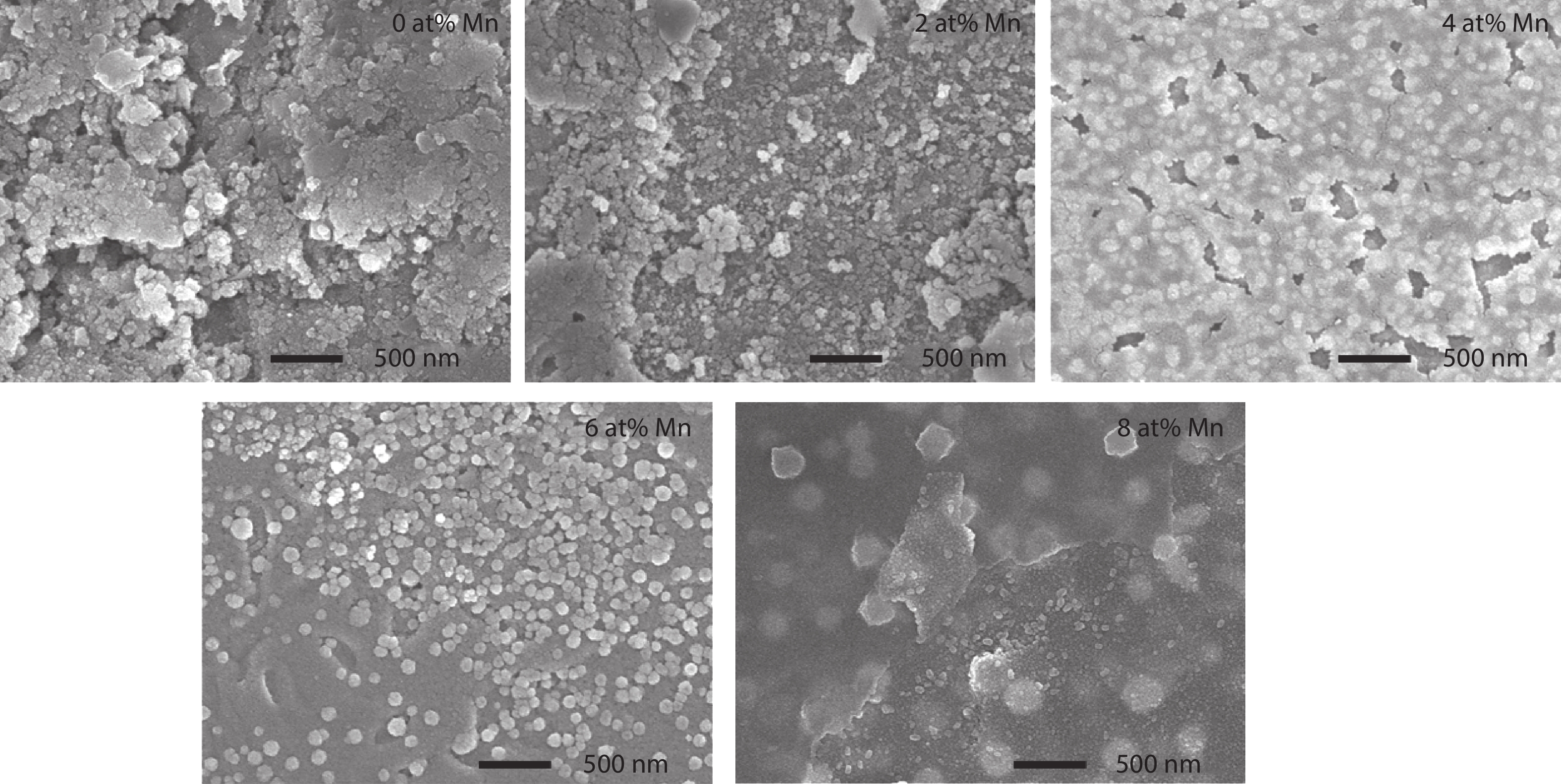
Fig. 1.
FESEM images of Mn:CuO thin films.
ARTICLES
R. Rahaman, M. Sharmin and J. Podder
Corresponding author: J. Podder, jpodder59@gmail.com
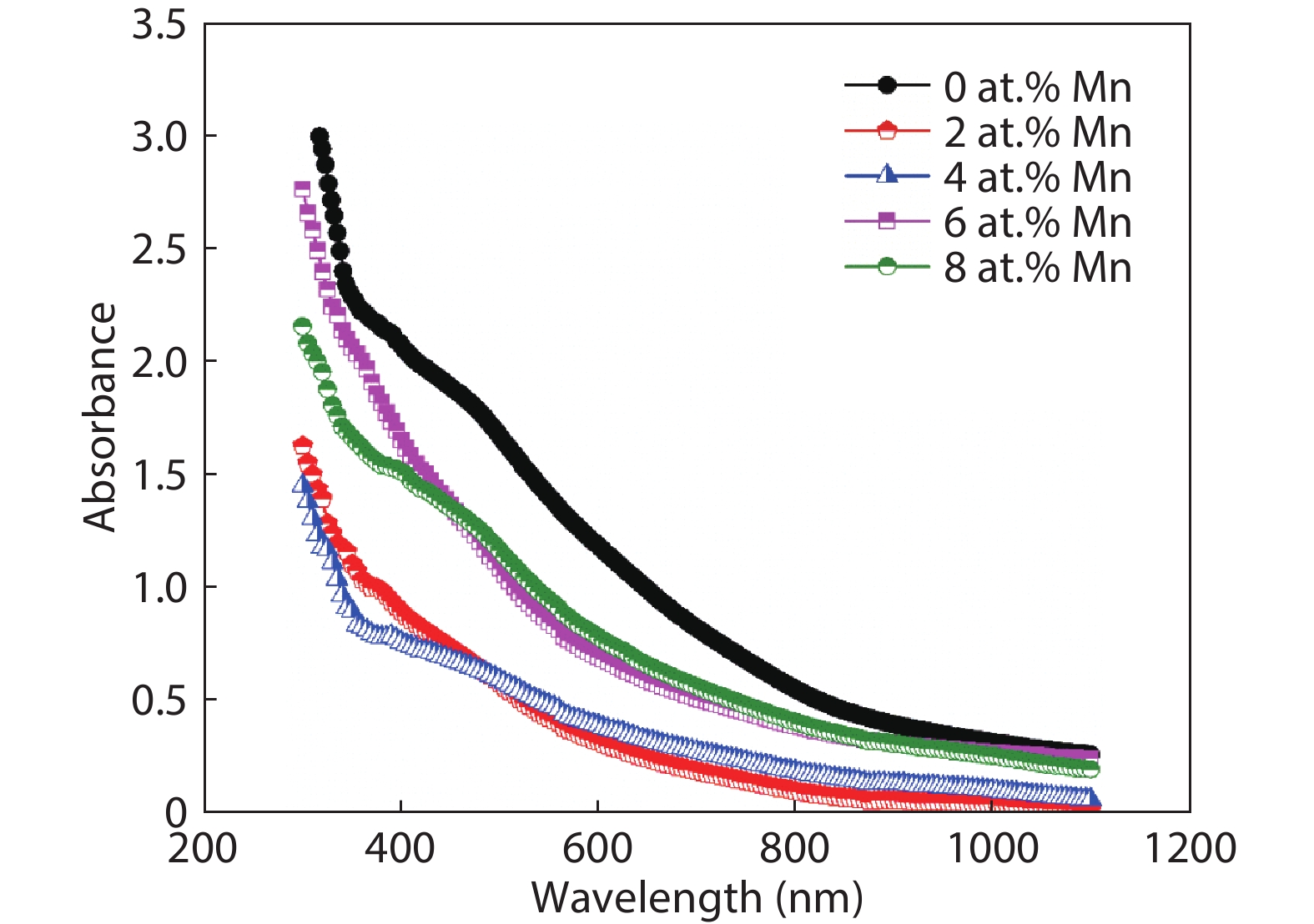
Abstract: Here we discuss the synthesis of copper (II) oxide (CuO) and manganese (Mn)-doped CuO thin films varying with 0 to 8 at% Mn using the spray pyrolysis technique. As-deposited film surfaces comprised of agglomerated spherical nanoparticles and a semi-spongy porous structure for 4 at% Mn doping. Energy dispersive analysis of X-rays confirmed the chemical composition of the films. X-ray diffraction spectra showed a polycrystalline monoclinic structure with the predominance of the (
Key words: Mn:CuO, spray pyrolysis, FESEM, XRD, band gap, Hall effect
| [1] |
Yoon K H, Choi W J, Kang D H. Photoelectrochemical properties of copper oxide thin films coated on an n-Si substrate. Thin Solid Films, 2000, 372, 250 doi: 10.1016/S0040-6090(00)01058-0
|
| [2] |
de Los Santos Valladares L, Salinas D H, Dominguez A B, et al. Crystallization and electrical resistivity of Cu2O and CuO obtained by thermal oxidation of Cu thin films on SiO2/Si substrates. Thin Solid Films, 2012, 520, 6368 doi: 10.1016/j.tsf.2012.06.043
|
| [3] |
Chang S S, Lee H J, Park H J. Photoluminescence properties of spark-processed CuO. Ceram Int, 2005, 31, 411 doi: 10.1016/j.ceramint.2004.05.027
|
| [4] |
Han K, Tao M. Electrochemically deposited p-n homojunction cuprous oxide solar cells. Sol Energy Mater Sol Cells, 2009, 93, 153 doi: 10.1016/j.solmat.2008.09.023
|
| [5] |
Steinhauer S, Brunet E, Maier T, et al. Gas sensing properties of novel CuO nanowire devices. Sens Actuators B, 2013, 187, 50 doi: 10.1016/j.snb.2012.09.034
|
| [6] |
Ren G G, Hu D W, Cheng E W C, et al. Characterisation of copper oxide nanoparticles for antimicrobial applications. Int J Antimicrob Agents, 2009, 33, 587 doi: 10.1016/j.ijantimicag.2008.12.004
|
| [7] |
Erdoğan İ Y, Güllü Ö. Optical and structural properties of CuO nanofilm: Its diode application. J Alloys Compd, 2010, 492, 378 doi: 10.1016/j.jallcom.2009.11.109
|
| [8] |
Al-Kuhaili M F. Characterization of copper oxide thin films deposited by the thermal evaporation of cuprous oxide (Cu2O). Vacuum, 2008, 82, 623 doi: 10.1016/j.vacuum.2007.10.004
|
| [9] |
Kikuchi N, Tonooka K. Electrical and structural properties of Ni-doped Cu2O films prepared by pulsed laser deposition. Thin Solid Films, 2005, 486, 33 doi: 10.1016/j.tsf.2004.12.044
|
| [10] |
Eisermann S, Kronenberger A, Laufer A, et al. Copper oxide thin films by chemical vapor deposition: Synthesis, characterization and electrical properties. Phys Status Solidi A, 2012, 209, 531 doi: 10.1002/pssa.201127493
|
| [11] |
Brazdeikis A, Karlsson U O, Flodström A S. An atomic force microscopy study of thin copper oxide films grown by molecular beam epitaxy on MgO(100). Thin Solid Films, 1996, 281/282, 57 doi: 10.1016/0040-6090(96)08574-4
|
| [12] |
Perednis D, Gauckler L J. Thin film deposition using spray pyrolysis. J Electroceramics, 2005, 14, 103 doi: 10.1007/s10832-005-0870-x
|
| [13] |
Nesa M, Sharmin M, Hossain K S, et al. Structural, morphological, optical and electrical properties of spray deposited zinc doped copper oxide thin films. J Mater Sci: Mater Electron, 2017, 28, 12523 doi: 10.1007/s10854-017-7075-3
|
| [14] |
Gülen Y, Bayansal F, Şahin B, et al. Fabrication and characterization of Mn-doped CuO thin films by the SILAR method. Ceram Int, 2013, 39, 6475 doi: 10.1016/j.ceramint.2013.01.077
|
| [15] |
Bayansal F, Taşköprü T, Şahin B, et al. Effect of cobalt doping on nanostructured CuO thin films. Metall And Mat Trans A, 2014, 45, 3670 doi: 10.1007/s11661-014-2306-1
|
| [16] |
Shannon R D. Revised effective ionic radii and systematic studies of interatomic distances in halides and chalcogenides. Acta Crystallogr Sect A, 1976, 32, 751 doi: 10.1107/S0567739476001551
|
| [17] |
Zhao F, Qiu H M, Pan L Q, et al. Ferromagnetism analysis of Mn-doped CuO thin films. J Phys: Condens Matter, 2008, 20, 425208 doi: 10.1088/0953-8984/20/42/425208
|
| [18] |
Li L, Lv B, Wang S, et al. Magnetic study of heavily Mn-doped CuO thin films. J Korean Phys Soc, 2013, 62, 1530 doi: 10.3938/jkps.62.1530
|
| [19] |
Ganesan K P, Anandhan N, Gopu G, et al. An enhancement of ferromagnetic, structural, morphological, and optical properties of Mn-doped Cu2O thin films by an electrodeposition technique. J Mater Sci: Mater Electron, 2019, 30, 19524 doi: 10.1007/s10854-019-02318-5
|
| [20] |
Durai G, Kuppusami P, Viswanathan K. Investigation on microstructure and improved supercapacitive performance of Mn doped CuO thin films prepared by reactive radio frequency magnetron sputtering. J Mater Sci: Mater Electron, 2018, 29, 2051 doi: 10.1007/s10854-017-8118-5
|
| [21] |
Mishjil K A, Qader K, Jabbar W A. Study the effect of Mn:CuO thin film on its optical properties. Mater Sci, 2015, 13, 388
|
| [22] |
Albert manoharan A, Chandramohan R, David prabu R, et al. Facile synthesis and characterization of undoped, Mn doped and Nd co-doped CuO nanoparticles for optoelectronic and magnetic applications. J Mol Struct, 2018, 1171, 388 doi: 10.1016/j.molstruc.2018.06.018
|
| [23] |
Tolansky S. Multiple beam interferometry of surfaces and films. London: Oxford Clarendon Press, 1948
|
| [24] |
Iqbal M, Thebo A A, Shah A H, et al. Influence of Mn-doping on the photocatalytic and solar cell efficiency of CuO nanowires. Inorg Chem Commun, 2017, 76, 71 doi: 10.1016/j.inoche.2016.11.023
|
| [25] |
Babu M H, Podder J, Dev B C, et al. P to n-type transition with wide blue shift optical band gap of spray synthesized Cd doped CuO thin films for optoelectronic device applications. Surf Interfaces, 2020, 19, 100459 doi: 10.1016/j.surfin.2020.100459
|
| [26] |
Chtouki T, Taboukhat S, Kavak H, et al. Characterization and third harmonic generation calculations of undoped and doped spin-coated multilayered CuO thin films. J Phys Chem Solids, 2019, 124, 60 doi: 10.1016/j.jpcs.2018.08.035
|
| [27] |
Lupan O, Cretu V, Postica V, et al. Enhanced ethanol vapour sensing performances of copper oxide nanocrystals with mixed phases. Sens Actuators B., 2016, 224, 434 doi: 10.1016/j.snb.2015.10.042
|
| [28] |
Scherrer P. Bestimmung der inneren Struktur und der Größe von Kolloidteilchen mittels Röntgenstrahlen. Kolloidchemie Ein Lehrbuch. Berlin, Heidelberg: Springer, 1912, 387 doi: 10.1007/978-3-662-33915-2_7
|
| [29] |
Zhao Y S, Zhang J Z. Microstrain and grain-size analysis from diffraction peak width and graphical derivation of high-pressure thermomechanics. J Appl Cryst, 2008, 41, 1095 doi: 10.1107/S0021889808031762
|
| [30] |
Smallman R E, Westmacott K H. Stacking faults in face-centred cubic metals and alloys. Philos Mag A, 1957, 2, 669 doi: 10.1080/14786435708242709
|
| [31] |
Williamson G K, Smallman R E. III. Dislocation densities in some annealed and cold-worked metals from measurements on the X-ray Debye-scherrer spectrum. Philos Mag A, 1956, 1, 34 doi: 10.1080/14786435608238074
|
| [32] |
Tauc J. Optical properties of amorphous semiconductors. Amorphous and Liquid Semiconductors. Boston, MA: Springer, 1974, 159 doi: 10.1007/978-1-4615-8705-7_4
|
| [33] |
Zheng W F, Chen Y, Peng X H, et al. The phase evolution and physical properties of binary copper oxide thin films prepared by reactive magnetron sputtering. Materials, 2018, 11, 1253 doi: 10.3390/ma11071253
|
| [34] |
Alajlani Y, Placido F, Barlow A, et al. Characterisation of Cu2O, Cu4O3, and CuO mixed phase thin films produced by microwave-activated reactive sputtering. Vacuum, 2017, 144, 217 doi: 10.1016/j.vacuum.2017.08.005
|
| [35] |
Moss T S. Photoconductivity in the elements. New York: Academic Press Inc, 1952 doi: 10.1088/0370-1298/64/6/113
|
| [36] |
Hervé P, Vandamme L K J. General relation between refractive index and energy gap in semiconductors. Infrared Phys Technol, 1994, 35, 609 doi: 10.1016/1350-4495(94)90026-4
|
| [37] |
Ravindra N M, Ganapathy P, Choi J. Energy gap-refractive index relations in semiconductors - An overview. Infrared Phys Technol, 2007, 50, 21 doi: 10.1016/j.infrared.2006.04.001
|
| [38] |
Moumen A, Hartiti B, Thevenin P, et al. Synthesis and characterization of CuO thin films grown by chemical spray pyrolysis. Opt Quantum Electron, 2017, 49, 1 doi: 10.1007/s11082-016-0848-8
|
| [39] |
Dhanasekaran V, Mahalingam T. Electrochemical and physical properties of electroplated CuO thin films. J Nanosci Nanotechnol, 2013, 13, 250 doi: 10.1166/jnn.2013.6709
|
| [40] |
Hummel R E. Hummel R E. Electronic properties of materials. New York, NY: Springer, 2011 doi: 10.1007/978-1-4419-8164-6
|
| [41] |
Adachi S. Properties of group-IV, III-V and II-VI semiconductors. Chichester, UK: John Wiley & Sons, Ltd, 2005 doi: 10.1002/0470090340
|
| [42] |
Akaltun Y. Effect of thickness on the structural and optical properties of CuO thin films grown by successive ionic layer adsorption and reaction. Thin Solid Films, 2015, 594, 30 doi: 10.1016/j.tsf.2015.10.003
|
| [43] |
Güneri E. The role of Au doping on the structural and optical properties of Cu2O films. J Nano Res, 2019, 58, 49 doi: 10.4028/www.scientific.net/JNanoR.58.49
|
| [44] |
Baturay S, Tombak A, Kaya D, et al. Modification of electrical and optical properties of CuO thin films by Ni doping. J Sol Gel Sci Technol, 2016, 78, 422 doi: 10.1007/s10971-015-3953-4
|
| [45] |
Sanal K C, Vikas L S, Jayaraj M K. Room temperature deposited transparent p-channel CuO thin film transistors. Appl Surf Sci, 2014, 297, 153 doi: 10.1016/j.apsusc.2014.01.109
|
| [46] |
Shen Y L, Guo M L, Xia X H, et al. Role of materials chemistry on the electrical/electronic properties of CuO thin films. Acta Mater, 2015, 85, 122 doi: 10.1016/j.actamat.2014.11.018
|

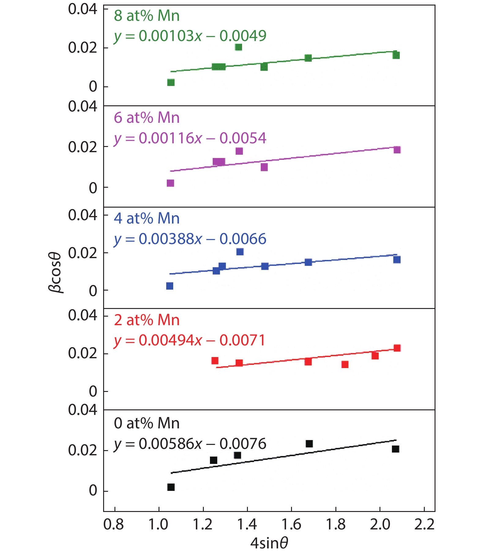


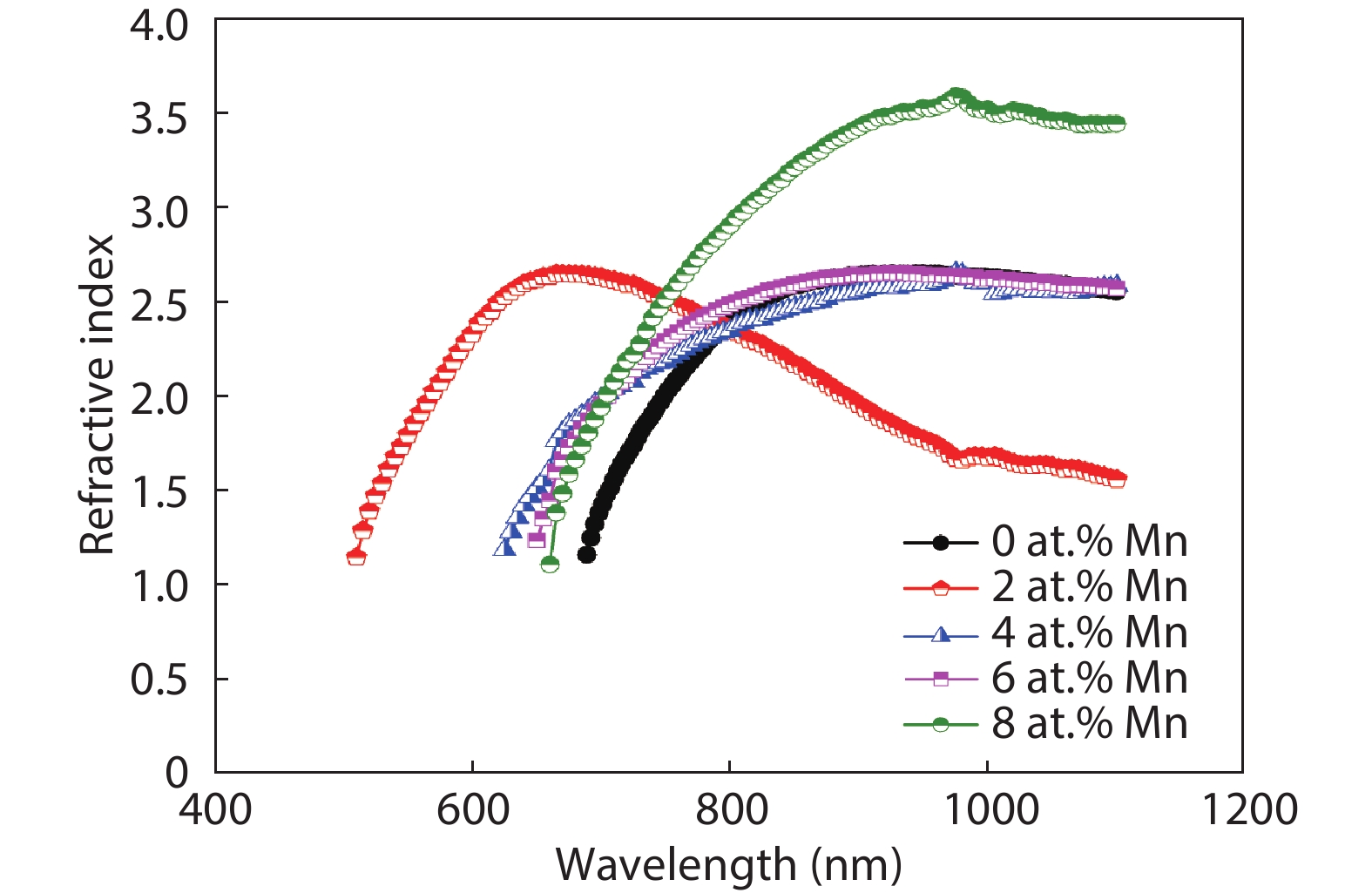
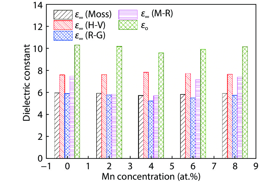
Table 1. Parameters of CuO and Mn:CuO thin film deposition.
| Parameter | Condition |
| Spray rate during deposition | 1.00 mL/min |
| Substrate temperature | 350 °C |
| Deposition time | 10 min |
| Nozzle-to-substrate distance | 25 cm |
| Carrier air pressure | 0.50 bar |
 DownLoad: CSV
Table 2. Quantitative results from EDX analysis of CuO and Mn:CuO thin films.
| Mn conc. in CuO (at%) | at.% of element in EDX report | Mn/Cu ratio | |||||
| O | σO | Cu | σCu | Mn | σMn | ||
| 0 | 40.81 | 0.18 | 58.19 | 0.48 | – | – | 0 |
| 2 | 66.36 | 0.38 | 33.42 | 0.45 | 0.21 | 0.33 | 0.006 |
| 4 | 75.68 | 0.44 | 23.20 | 0.43 | 1.12 | 0.42 | 0.048 |
| 6 | 60.82 | 0.33 | 35.55 | 0.44 | 3.63 | 0.42 | 0.102 |
| 8 | 54.58 | 0.20 | 41.26 | 0.41 | 4.17 | 0.39 | 0.101 |
DownLoad: CSV
Table 3. Structural parameters of CuO and Mn:CuO thin films.
| Mn conc. (at.%) | 2θ (deg) | (hkl) | D (nm) | Davg (nm) | ε (10–3) | δ (10–3) |
| 0 | 36.3809 | ( | 18.80 | 17.60 | 1.60 | 3.20 |
| 39.6309 | (200) | 16.30 | ||||
| 2 | 36.5833 | ( | 18.80 | 17.50 | 1.61 | 3.30 |
| 39.8928 | (200) | 16.20 | ||||
| 4 | 36.7023 | ( | 22.60 | 18.50 | 1.50 | 2.90 |
| 39.9642 | (200) | 14.30 | ||||
| 6 | 36.7024 | ( | 22.60 | 19.50 | 1.41 | 2.60 |
| 39.8333 | (200) | 16.30 | ||||
| 8 | 36.6429 | ( | 28.20 | 21.30 | 1.32 | 2.40 |
| 39.8095 | (200) | 14.30 |
DownLoad: CSV
Table 4. Optical parameters of CuO and Mn:CuO thin films.
| Mn Conc. (at%) | n (Moss) | n (H-V) | n (R-G) | ε∞ (Moss) | ε∞ (H-V) | ε∞ (R-G) | ε∞ (M-R) | εo | |
| 0 | 2.44 | 2.75 | 2.43 | 5.96 | 7.59 | 5.90 | 7.47 | 10.30 | 0.18 |
| 2 | 2.43 | 2.76 | 2.40 | 5.92 | 7.62 | 5.78 | 5.84 | 10.17 | 0.17 |
| 4 | 2.39 | 2.80 | 2.29 | 5.72 | 7.82 | 5.22 | 5.69 | 9.59 | 0.04 |
| 6 | 2.41 | 2.78 | 2.35 | 5.82 | 7.71 | 5.51 | 7.16 | 9.90 | 0.12 |
| 8 | 2.43 | 2.76 | 2.39 | 5.91 | 7.64 | 5.75 | 7.40 | 10.14 | 0.16 |
DownLoad: CSV
| [1] |
Yoon K H, Choi W J, Kang D H. Photoelectrochemical properties of copper oxide thin films coated on an n-Si substrate. Thin Solid Films, 2000, 372, 250 doi: 10.1016/S0040-6090(00)01058-0
|
| [2] |
de Los Santos Valladares L, Salinas D H, Dominguez A B, et al. Crystallization and electrical resistivity of Cu2O and CuO obtained by thermal oxidation of Cu thin films on SiO2/Si substrates. Thin Solid Films, 2012, 520, 6368 doi: 10.1016/j.tsf.2012.06.043
|
| [3] |
Chang S S, Lee H J, Park H J. Photoluminescence properties of spark-processed CuO. Ceram Int, 2005, 31, 411 doi: 10.1016/j.ceramint.2004.05.027
|
| [4] |
Han K, Tao M. Electrochemically deposited p-n homojunction cuprous oxide solar cells. Sol Energy Mater Sol Cells, 2009, 93, 153 doi: 10.1016/j.solmat.2008.09.023
|
| [5] |
Steinhauer S, Brunet E, Maier T, et al. Gas sensing properties of novel CuO nanowire devices. Sens Actuators B, 2013, 187, 50 doi: 10.1016/j.snb.2012.09.034
|
| [6] |
Ren G G, Hu D W, Cheng E W C, et al. Characterisation of copper oxide nanoparticles for antimicrobial applications. Int J Antimicrob Agents, 2009, 33, 587 doi: 10.1016/j.ijantimicag.2008.12.004
|
| [7] |
Erdoğan İ Y, Güllü Ö. Optical and structural properties of CuO nanofilm: Its diode application. J Alloys Compd, 2010, 492, 378 doi: 10.1016/j.jallcom.2009.11.109
|
| [8] |
Al-Kuhaili M F. Characterization of copper oxide thin films deposited by the thermal evaporation of cuprous oxide (Cu2O). Vacuum, 2008, 82, 623 doi: 10.1016/j.vacuum.2007.10.004
|
| [9] |
Kikuchi N, Tonooka K. Electrical and structural properties of Ni-doped Cu2O films prepared by pulsed laser deposition. Thin Solid Films, 2005, 486, 33 doi: 10.1016/j.tsf.2004.12.044
|
| [10] |
Eisermann S, Kronenberger A, Laufer A, et al. Copper oxide thin films by chemical vapor deposition: Synthesis, characterization and electrical properties. Phys Status Solidi A, 2012, 209, 531 doi: 10.1002/pssa.201127493
|
| [11] |
Brazdeikis A, Karlsson U O, Flodström A S. An atomic force microscopy study of thin copper oxide films grown by molecular beam epitaxy on MgO(100). Thin Solid Films, 1996, 281/282, 57 doi: 10.1016/0040-6090(96)08574-4
|
| [12] |
Perednis D, Gauckler L J. Thin film deposition using spray pyrolysis. J Electroceramics, 2005, 14, 103 doi: 10.1007/s10832-005-0870-x
|
| [13] |
Nesa M, Sharmin M, Hossain K S, et al. Structural, morphological, optical and electrical properties of spray deposited zinc doped copper oxide thin films. J Mater Sci: Mater Electron, 2017, 28, 12523 doi: 10.1007/s10854-017-7075-3
|
| [14] |
Gülen Y, Bayansal F, Şahin B, et al. Fabrication and characterization of Mn-doped CuO thin films by the SILAR method. Ceram Int, 2013, 39, 6475 doi: 10.1016/j.ceramint.2013.01.077
|
| [15] |
Bayansal F, Taşköprü T, Şahin B, et al. Effect of cobalt doping on nanostructured CuO thin films. Metall And Mat Trans A, 2014, 45, 3670 doi: 10.1007/s11661-014-2306-1
|
| [16] |
Shannon R D. Revised effective ionic radii and systematic studies of interatomic distances in halides and chalcogenides. Acta Crystallogr Sect A, 1976, 32, 751 doi: 10.1107/S0567739476001551
|
| [17] |
Zhao F, Qiu H M, Pan L Q, et al. Ferromagnetism analysis of Mn-doped CuO thin films. J Phys: Condens Matter, 2008, 20, 425208 doi: 10.1088/0953-8984/20/42/425208
|
| [18] |
Li L, Lv B, Wang S, et al. Magnetic study of heavily Mn-doped CuO thin films. J Korean Phys Soc, 2013, 62, 1530 doi: 10.3938/jkps.62.1530
|
| [19] |
Ganesan K P, Anandhan N, Gopu G, et al. An enhancement of ferromagnetic, structural, morphological, and optical properties of Mn-doped Cu2O thin films by an electrodeposition technique. J Mater Sci: Mater Electron, 2019, 30, 19524 doi: 10.1007/s10854-019-02318-5
|
| [20] |
Durai G, Kuppusami P, Viswanathan K. Investigation on microstructure and improved supercapacitive performance of Mn doped CuO thin films prepared by reactive radio frequency magnetron sputtering. J Mater Sci: Mater Electron, 2018, 29, 2051 doi: 10.1007/s10854-017-8118-5
|
| [21] |
Mishjil K A, Qader K, Jabbar W A. Study the effect of Mn:CuO thin film on its optical properties. Mater Sci, 2015, 13, 388
|
| [22] |
Albert manoharan A, Chandramohan R, David prabu R, et al. Facile synthesis and characterization of undoped, Mn doped and Nd co-doped CuO nanoparticles for optoelectronic and magnetic applications. J Mol Struct, 2018, 1171, 388 doi: 10.1016/j.molstruc.2018.06.018
|
| [23] |
Tolansky S. Multiple beam interferometry of surfaces and films. London: Oxford Clarendon Press, 1948
|
| [24] |
Iqbal M, Thebo A A, Shah A H, et al. Influence of Mn-doping on the photocatalytic and solar cell efficiency of CuO nanowires. Inorg Chem Commun, 2017, 76, 71 doi: 10.1016/j.inoche.2016.11.023
|
| [25] |
Babu M H, Podder J, Dev B C, et al. P to n-type transition with wide blue shift optical band gap of spray synthesized Cd doped CuO thin films for optoelectronic device applications. Surf Interfaces, 2020, 19, 100459 doi: 10.1016/j.surfin.2020.100459
|
| [26] |
Chtouki T, Taboukhat S, Kavak H, et al. Characterization and third harmonic generation calculations of undoped and doped spin-coated multilayered CuO thin films. J Phys Chem Solids, 2019, 124, 60 doi: 10.1016/j.jpcs.2018.08.035
|
| [27] |
Lupan O, Cretu V, Postica V, et al. Enhanced ethanol vapour sensing performances of copper oxide nanocrystals with mixed phases. Sens Actuators B., 2016, 224, 434 doi: 10.1016/j.snb.2015.10.042
|
| [28] |
Scherrer P. Bestimmung der inneren Struktur und der Größe von Kolloidteilchen mittels Röntgenstrahlen. Kolloidchemie Ein Lehrbuch. Berlin, Heidelberg: Springer, 1912, 387 doi: 10.1007/978-3-662-33915-2_7
|
| [29] |
Zhao Y S, Zhang J Z. Microstrain and grain-size analysis from diffraction peak width and graphical derivation of high-pressure thermomechanics. J Appl Cryst, 2008, 41, 1095 doi: 10.1107/S0021889808031762
|
| [30] |
Smallman R E, Westmacott K H. Stacking faults in face-centred cubic metals and alloys. Philos Mag A, 1957, 2, 669 doi: 10.1080/14786435708242709
|
| [31] |
Williamson G K, Smallman R E. III. Dislocation densities in some annealed and cold-worked metals from measurements on the X-ray Debye-scherrer spectrum. Philos Mag A, 1956, 1, 34 doi: 10.1080/14786435608238074
|
| [32] |
Tauc J. Optical properties of amorphous semiconductors. Amorphous and Liquid Semiconductors. Boston, MA: Springer, 1974, 159 doi: 10.1007/978-1-4615-8705-7_4
|
| [33] |
Zheng W F, Chen Y, Peng X H, et al. The phase evolution and physical properties of binary copper oxide thin films prepared by reactive magnetron sputtering. Materials, 2018, 11, 1253 doi: 10.3390/ma11071253
|
| [34] |
Alajlani Y, Placido F, Barlow A, et al. Characterisation of Cu2O, Cu4O3, and CuO mixed phase thin films produced by microwave-activated reactive sputtering. Vacuum, 2017, 144, 217 doi: 10.1016/j.vacuum.2017.08.005
|
| [35] |
Moss T S. Photoconductivity in the elements. New York: Academic Press Inc, 1952 doi: 10.1088/0370-1298/64/6/113
|
| [36] |
Hervé P, Vandamme L K J. General relation between refractive index and energy gap in semiconductors. Infrared Phys Technol, 1994, 35, 609 doi: 10.1016/1350-4495(94)90026-4
|
| [37] |
Ravindra N M, Ganapathy P, Choi J. Energy gap-refractive index relations in semiconductors - An overview. Infrared Phys Technol, 2007, 50, 21 doi: 10.1016/j.infrared.2006.04.001
|
| [38] |
Moumen A, Hartiti B, Thevenin P, et al. Synthesis and characterization of CuO thin films grown by chemical spray pyrolysis. Opt Quantum Electron, 2017, 49, 1 doi: 10.1007/s11082-016-0848-8
|
| [39] |
Dhanasekaran V, Mahalingam T. Electrochemical and physical properties of electroplated CuO thin films. J Nanosci Nanotechnol, 2013, 13, 250 doi: 10.1166/jnn.2013.6709
|
| [40] |
Hummel R E. Hummel R E. Electronic properties of materials. New York, NY: Springer, 2011 doi: 10.1007/978-1-4419-8164-6
|
| [41] |
Adachi S. Properties of group-IV, III-V and II-VI semiconductors. Chichester, UK: John Wiley & Sons, Ltd, 2005 doi: 10.1002/0470090340
|
| [42] |
Akaltun Y. Effect of thickness on the structural and optical properties of CuO thin films grown by successive ionic layer adsorption and reaction. Thin Solid Films, 2015, 594, 30 doi: 10.1016/j.tsf.2015.10.003
|
| [43] |
Güneri E. The role of Au doping on the structural and optical properties of Cu2O films. J Nano Res, 2019, 58, 49 doi: 10.4028/www.scientific.net/JNanoR.58.49
|
| [44] |
Baturay S, Tombak A, Kaya D, et al. Modification of electrical and optical properties of CuO thin films by Ni doping. J Sol Gel Sci Technol, 2016, 78, 422 doi: 10.1007/s10971-015-3953-4
|
| [45] |
Sanal K C, Vikas L S, Jayaraj M K. Room temperature deposited transparent p-channel CuO thin film transistors. Appl Surf Sci, 2014, 297, 153 doi: 10.1016/j.apsusc.2014.01.109
|
| [46] |
Shen Y L, Guo M L, Xia X H, et al. Role of materials chemistry on the electrical/electronic properties of CuO thin films. Acta Mater, 2015, 85, 122 doi: 10.1016/j.actamat.2014.11.018
|


Article views: 2198 Times PDF downloads: 107 Times Cited by: 0 Times
Received: 07 May 2021 Revised: 21 August 2021 Online: Accepted Manuscript: 04 November 2021Uncorrected proof: 09 November 2021Published: 04 January 2022
| Citation: |
R. Rahaman, M. Sharmin, J. Podder. Band gap tuning and p to n-type transition in Mn-doped CuO nanostructured thin films[J]. Journal of Semiconductors, 2022, 43(1): 012801. doi: 10.1088/1674-4926/43/1/012801
R Rahaman, M Sharmin, J Podder, Band gap tuning and p to n-type transition in Mn-doped CuO nanostructured thin films[J]. J. Semicond., 2022, 43(1): 012801. doi: 10.1088/1674-4926/43/1/012801.
Export: BibTex EndNote

|
| [1] |
Yoon K H, Choi W J, Kang D H. Photoelectrochemical properties of copper oxide thin films coated on an n-Si substrate. Thin Solid Films, 2000, 372, 250 doi: 10.1016/S0040-6090(00)01058-0
|
| [2] |
de Los Santos Valladares L, Salinas D H, Dominguez A B, et al. Crystallization and electrical resistivity of Cu2O and CuO obtained by thermal oxidation of Cu thin films on SiO2/Si substrates. Thin Solid Films, 2012, 520, 6368 doi: 10.1016/j.tsf.2012.06.043
|
| [3] |
Chang S S, Lee H J, Park H J. Photoluminescence properties of spark-processed CuO. Ceram Int, 2005, 31, 411 doi: 10.1016/j.ceramint.2004.05.027
|
| [4] |
Han K, Tao M. Electrochemically deposited p-n homojunction cuprous oxide solar cells. Sol Energy Mater Sol Cells, 2009, 93, 153 doi: 10.1016/j.solmat.2008.09.023
|
| [5] |
Steinhauer S, Brunet E, Maier T, et al. Gas sensing properties of novel CuO nanowire devices. Sens Actuators B, 2013, 187, 50 doi: 10.1016/j.snb.2012.09.034
|
| [6] |
Ren G G, Hu D W, Cheng E W C, et al. Characterisation of copper oxide nanoparticles for antimicrobial applications. Int J Antimicrob Agents, 2009, 33, 587 doi: 10.1016/j.ijantimicag.2008.12.004
|
| [7] |
Erdoğan İ Y, Güllü Ö. Optical and structural properties of CuO nanofilm: Its diode application. J Alloys Compd, 2010, 492, 378 doi: 10.1016/j.jallcom.2009.11.109
|
| [8] |
Al-Kuhaili M F. Characterization of copper oxide thin films deposited by the thermal evaporation of cuprous oxide (Cu2O). Vacuum, 2008, 82, 623 doi: 10.1016/j.vacuum.2007.10.004
|
| [9] |
Kikuchi N, Tonooka K. Electrical and structural properties of Ni-doped Cu2O films prepared by pulsed laser deposition. Thin Solid Films, 2005, 486, 33 doi: 10.1016/j.tsf.2004.12.044
|
| [10] |
Eisermann S, Kronenberger A, Laufer A, et al. Copper oxide thin films by chemical vapor deposition: Synthesis, characterization and electrical properties. Phys Status Solidi A, 2012, 209, 531 doi: 10.1002/pssa.201127493
|
| [11] |
Brazdeikis A, Karlsson U O, Flodström A S. An atomic force microscopy study of thin copper oxide films grown by molecular beam epitaxy on MgO(100). Thin Solid Films, 1996, 281/282, 57 doi: 10.1016/0040-6090(96)08574-4
|
| [12] |
Perednis D, Gauckler L J. Thin film deposition using spray pyrolysis. J Electroceramics, 2005, 14, 103 doi: 10.1007/s10832-005-0870-x
|
| [13] |
Nesa M, Sharmin M, Hossain K S, et al. Structural, morphological, optical and electrical properties of spray deposited zinc doped copper oxide thin films. J Mater Sci: Mater Electron, 2017, 28, 12523 doi: 10.1007/s10854-017-7075-3
|
| [14] |
Gülen Y, Bayansal F, Şahin B, et al. Fabrication and characterization of Mn-doped CuO thin films by the SILAR method. Ceram Int, 2013, 39, 6475 doi: 10.1016/j.ceramint.2013.01.077
|
| [15] |
Bayansal F, Taşköprü T, Şahin B, et al. Effect of cobalt doping on nanostructured CuO thin films. Metall And Mat Trans A, 2014, 45, 3670 doi: 10.1007/s11661-014-2306-1
|
| [16] |
Shannon R D. Revised effective ionic radii and systematic studies of interatomic distances in halides and chalcogenides. Acta Crystallogr Sect A, 1976, 32, 751 doi: 10.1107/S0567739476001551
|
| [17] |
Zhao F, Qiu H M, Pan L Q, et al. Ferromagnetism analysis of Mn-doped CuO thin films. J Phys: Condens Matter, 2008, 20, 425208 doi: 10.1088/0953-8984/20/42/425208
|
| [18] |
Li L, Lv B, Wang S, et al. Magnetic study of heavily Mn-doped CuO thin films. J Korean Phys Soc, 2013, 62, 1530 doi: 10.3938/jkps.62.1530
|
| [19] |
Ganesan K P, Anandhan N, Gopu G, et al. An enhancement of ferromagnetic, structural, morphological, and optical properties of Mn-doped Cu2O thin films by an electrodeposition technique. J Mater Sci: Mater Electron, 2019, 30, 19524 doi: 10.1007/s10854-019-02318-5
|
| [20] |
Durai G, Kuppusami P, Viswanathan K. Investigation on microstructure and improved supercapacitive performance of Mn doped CuO thin films prepared by reactive radio frequency magnetron sputtering. J Mater Sci: Mater Electron, 2018, 29, 2051 doi: 10.1007/s10854-017-8118-5
|
| [21] |
Mishjil K A, Qader K, Jabbar W A. Study the effect of Mn:CuO thin film on its optical properties. Mater Sci, 2015, 13, 388
|
| [22] |
Albert manoharan A, Chandramohan R, David prabu R, et al. Facile synthesis and characterization of undoped, Mn doped and Nd co-doped CuO nanoparticles for optoelectronic and magnetic applications. J Mol Struct, 2018, 1171, 388 doi: 10.1016/j.molstruc.2018.06.018
|
| [23] |
Tolansky S. Multiple beam interferometry of surfaces and films. London: Oxford Clarendon Press, 1948
|
| [24] |
Iqbal M, Thebo A A, Shah A H, et al. Influence of Mn-doping on the photocatalytic and solar cell efficiency of CuO nanowires. Inorg Chem Commun, 2017, 76, 71 doi: 10.1016/j.inoche.2016.11.023
|
| [25] |
Babu M H, Podder J, Dev B C, et al. P to n-type transition with wide blue shift optical band gap of spray synthesized Cd doped CuO thin films for optoelectronic device applications. Surf Interfaces, 2020, 19, 100459 doi: 10.1016/j.surfin.2020.100459
|
| [26] |
Chtouki T, Taboukhat S, Kavak H, et al. Characterization and third harmonic generation calculations of undoped and doped spin-coated multilayered CuO thin films. J Phys Chem Solids, 2019, 124, 60 doi: 10.1016/j.jpcs.2018.08.035
|
| [27] |
Lupan O, Cretu V, Postica V, et al. Enhanced ethanol vapour sensing performances of copper oxide nanocrystals with mixed phases. Sens Actuators B., 2016, 224, 434 doi: 10.1016/j.snb.2015.10.042
|
| [28] |
Scherrer P. Bestimmung der inneren Struktur und der Größe von Kolloidteilchen mittels Röntgenstrahlen. Kolloidchemie Ein Lehrbuch. Berlin, Heidelberg: Springer, 1912, 387 doi: 10.1007/978-3-662-33915-2_7
|
| [29] |
Zhao Y S, Zhang J Z. Microstrain and grain-size analysis from diffraction peak width and graphical derivation of high-pressure thermomechanics. J Appl Cryst, 2008, 41, 1095 doi: 10.1107/S0021889808031762
|
| [30] |
Smallman R E, Westmacott K H. Stacking faults in face-centred cubic metals and alloys. Philos Mag A, 1957, 2, 669 doi: 10.1080/14786435708242709
|
| [31] |
Williamson G K, Smallman R E. III. Dislocation densities in some annealed and cold-worked metals from measurements on the X-ray Debye-scherrer spectrum. Philos Mag A, 1956, 1, 34 doi: 10.1080/14786435608238074
|
| [32] |
Tauc J. Optical properties of amorphous semiconductors. Amorphous and Liquid Semiconductors. Boston, MA: Springer, 1974, 159 doi: 10.1007/978-1-4615-8705-7_4
|
| [33] |
Zheng W F, Chen Y, Peng X H, et al. The phase evolution and physical properties of binary copper oxide thin films prepared by reactive magnetron sputtering. Materials, 2018, 11, 1253 doi: 10.3390/ma11071253
|
| [34] |
Alajlani Y, Placido F, Barlow A, et al. Characterisation of Cu2O, Cu4O3, and CuO mixed phase thin films produced by microwave-activated reactive sputtering. Vacuum, 2017, 144, 217 doi: 10.1016/j.vacuum.2017.08.005
|
| [35] |
Moss T S. Photoconductivity in the elements. New York: Academic Press Inc, 1952 doi: 10.1088/0370-1298/64/6/113
|
| [36] |
Hervé P, Vandamme L K J. General relation between refractive index and energy gap in semiconductors. Infrared Phys Technol, 1994, 35, 609 doi: 10.1016/1350-4495(94)90026-4
|
| [37] |
Ravindra N M, Ganapathy P, Choi J. Energy gap-refractive index relations in semiconductors - An overview. Infrared Phys Technol, 2007, 50, 21 doi: 10.1016/j.infrared.2006.04.001
|
| [38] |
Moumen A, Hartiti B, Thevenin P, et al. Synthesis and characterization of CuO thin films grown by chemical spray pyrolysis. Opt Quantum Electron, 2017, 49, 1 doi: 10.1007/s11082-016-0848-8
|
| [39] |
Dhanasekaran V, Mahalingam T. Electrochemical and physical properties of electroplated CuO thin films. J Nanosci Nanotechnol, 2013, 13, 250 doi: 10.1166/jnn.2013.6709
|
| [40] |
Hummel R E. Hummel R E. Electronic properties of materials. New York, NY: Springer, 2011 doi: 10.1007/978-1-4419-8164-6
|
| [41] |
Adachi S. Properties of group-IV, III-V and II-VI semiconductors. Chichester, UK: John Wiley & Sons, Ltd, 2005 doi: 10.1002/0470090340
|
| [42] |
Akaltun Y. Effect of thickness on the structural and optical properties of CuO thin films grown by successive ionic layer adsorption and reaction. Thin Solid Films, 2015, 594, 30 doi: 10.1016/j.tsf.2015.10.003
|
| [43] |
Güneri E. The role of Au doping on the structural and optical properties of Cu2O films. J Nano Res, 2019, 58, 49 doi: 10.4028/www.scientific.net/JNanoR.58.49
|
| [44] |
Baturay S, Tombak A, Kaya D, et al. Modification of electrical and optical properties of CuO thin films by Ni doping. J Sol Gel Sci Technol, 2016, 78, 422 doi: 10.1007/s10971-015-3953-4
|
| [45] |
Sanal K C, Vikas L S, Jayaraj M K. Room temperature deposited transparent p-channel CuO thin film transistors. Appl Surf Sci, 2014, 297, 153 doi: 10.1016/j.apsusc.2014.01.109
|
| [46] |
Shen Y L, Guo M L, Xia X H, et al. Role of materials chemistry on the electrical/electronic properties of CuO thin films. Acta Mater, 2015, 85, 122 doi: 10.1016/j.actamat.2014.11.018
|

 WeChat ID
Journal of Semiconductors © 2017 All Rights Reserved 京ICP备05085259号-2