


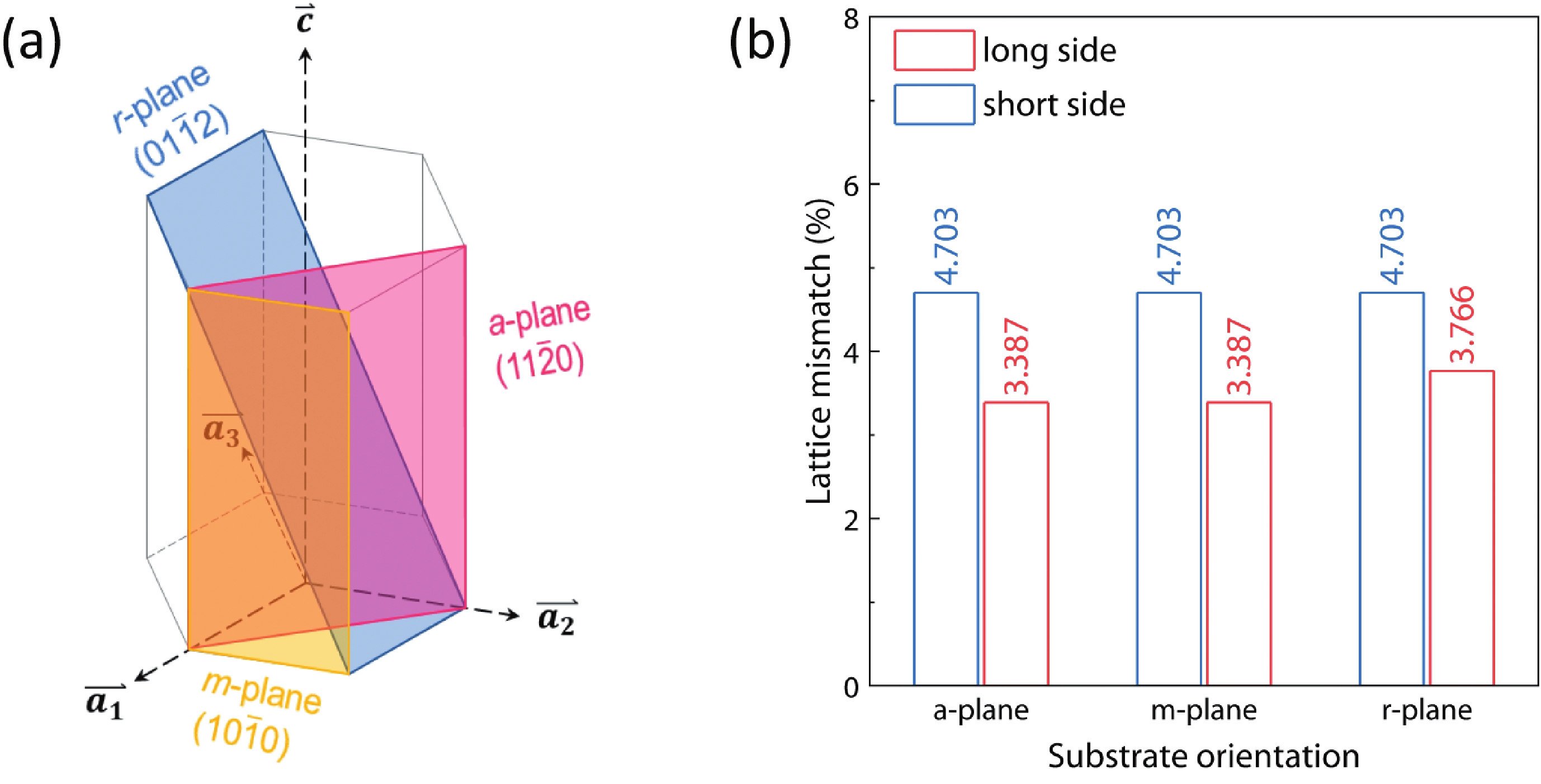
Fig. 1.
(Color online) (a) Schematic diagram of various crystal planes in the corundom structure. (b) The lattice mismatch between different crystal planes α-Ga2O3 films and corresponding sapphire substrates.
ARTICLES
Wei Wang1, 2, Shudong Hu1, Zilong Wang1, Kaisen Liu1, Jinfu Zhang1, Simiao Wu1, Yuxia Yang1, Ning Xia3, Wenrui Zhang1, 4, and Jichun Ye1, 4,
Corresponding author: Wenrui Zhang, zhangwenrui@nimte.ac.cn; Jichun Ye, jichun.ye@nimte.ac.cn
Abstract: This study explores the epitaxial relationship and electrical properties of α-Ga2O3 thin films deposited on a-plane, m-plane, and r-plane sapphire substrates. We characterize the thin films by X-ray diffraction and Raman spectroscopy, and elucidate thin film epitaxial relationships with the underlying sapphire substrates. The oxygen vacancy concentration of α-Ga2O3 thin films on m-plane and r-plane sapphire substrates are higher than α-Ga2O3 thin film on a-plane sapphire substrates. All three thin films have a high transmission of over 80% in the visible and near-ultraviolet regions, and their optical bandgaps stay around 5.02–5.16 eV. Hall measurements show that the α-Ga2O3 thin film grown on r-plane sapphire has the highest conductivity of 2.71 S/cm, which is at least 90 times higher than the film on a-plane sapphire. A similar orientation-dependence is seen in their activation energy as revealed by temperature-dependent conductivity measurements, with 0.266, 0.079, and 0.075 eV for the film on a-, m-, r-plane, respectively. The origin of the distinct transport behavior of films on differently oriented substrates is suggested to relate with the distinct evolution of oxygen vacancies at differently oriented substrates. This study provides insights for the substrate selection when growing α-Ga2O3 films with tunable transport properties.
Key words: gallium oxide, thin film epitaxy, orientation, oxygen vacancy, electrical properties
| [1] |
Konishi K, Goto K, Murakami H, et al. 1-kV vertical Ga2O3 field-plated Schottky barrier diodes. Appl Phys Lett, 2017, 110, 103506 doi: 10.1063/1.4977857
|
| [2] |
Hu Z Z, Zhou H, Feng Q, et al. Field-plated lateral β-Ga2O3 Schottky barrier diode with high reverse blocking voltage of more than 3 kV and high DC power figure-of-merit of 500 MW/cm2. IEEE Electron Device Lett, 2018, 39, 1564 doi: 10.1109/LED.2018.2868444
|
| [3] |
Hao W B, He Q M, Zhou X Z, et al. 2.6 kV NiO/Ga2O3 heterojunction diode with superior high-temperature voltage blocking capability. 2022 IEEE 34th International Symposium on Power Semiconductor Devices and ICs (ISPSD), 2022, 105 doi: 10.1109/ISPSD49238.2022.9813680
|
| [4] |
Gong H H, Chen X H, Xu Y, et al. A 1.86-kV double-layered NiO/β-Ga2O3 vertical p–n heterojunction diode. Appl Phys Lett, 2020, 117, 022104 doi: 10.1063/5.0010052
|
| [5] |
Zhou X Z, Ma Y J, Xu G W, et al. Enhancement-mode β-Ga2O3 U-shaped gate trench vertical MOSFET realized by oxygen annealing. Appl Phys Lett, 2022, 121, 223501 doi: 10.1063/5.0130292
|
| [6] |
Moser N, McCandless J, Crespo A, et al. Ge-doped β-Ga2O3 MOSFETs. IEEE Electron Device Lett, 2017, 38, 775 doi: 10.1109/LED.2017.2697359
|
| [7] |
Jinno R, Chang C S, Onuma T, et al. Crystal orientation dictated epitaxy of ultrawide-bandgap 5.4- to 8.6-eV α-(AlGa)2O3 on m-plane sapphire. Sci Adv, 2021, 7, eabd5891 doi: 10.1126/sciadv.abd5891
|
| [8] |
Kracht M, Karg A, Feneberg M, et al. Anisotropic optical properties of metastable (011-2) α–Ga2O3 grown by plasma-assisted molecular beam epitaxy. Phys Rev Applied, 2018, 10, 024047 doi: 10.1103/PhysRevApplied.10.024047
|
| [9] |
Wu Z Y, Jiang Z X, Song P Y, et al. Nanowire-seeded growth of single-crystalline (010) β-Ga2 O3 nanosheets with high field-effect electron mobility and on/off current ratio. Small, 2019, 15, e1900580 doi: 10.1002/smll.201900580
|
| [10] |
Zhang W R, Zhang J G, Chen L, et al. Non-equilibrium epitaxy of metastable polymorphs of ultrawide-bandgap gallium oxide. Appl Phys Lett, 2022, 120, 072101 doi: 10.1063/5.0078752
|
| [11] |
Zhang J G, Wang W, Wu S M, et al. Exploratory phase stabilization in heteroepitaxial gallium oxide films by pulsed laser deposition. J Alloys Compd, 2023, 935, 168123 doi: 10.1016/j.jallcom.2022.168123
|
| [12] |
Wu C, Guo D Y, Zhang L Y, et al. Systematic investigation of the growth kinetics of β-Ga2O3 epilayer by plasma enhanced chemical vapor deposition. Appl Phys Lett, 2020, 116, 072102 doi: 10.1063/1.5142196
|
| [13] |
Wang W, Yuan Q L, Han D Y, et al. High-temperature deep ultraviolet photodetector based on a crystalline Ga2O3-diamond heterostructure. IEEE Electron Device Lett, 2022, 43, 2121 doi: 10.1109/LED.2022.3214981
|
| [14] |
Zhang Y B, Zheng J, Ma P P, et al. Growth and characterization of β-Ga2O3 thin films grown on off-angled Al2O3 substrates by metal-organic chemical vapor deposition. J Semicond, 2022, 43, 092801 doi: 10.1088/1674-4926/43/9/092801
|
| [15] |
Sun H D, Li K H, Torres Castanedo C G, et al. HCl flow-induced phase change of α-, β-, and ε-Ga2O3 films grown by MOCVD. Cryst Growth Des, 2018, 18, 2370 doi: 10.1021/acs.cgd.7b01791
|
| [16] |
Hou X H, Sun H D, Long S B, et al. Ultrahigh-performance solar-blind photodetector based on α-phase-dominated Ga2O3 film with record low dark current of 81 fA. IEEE Electron Device Lett, 2019, 40, 1483 doi: 10.1109/LED.2019.2932140
|
| [17] |
Nakagomi S, Kokubun Y. Crystal orientation of β-Ga2O3 thin films formed on c-plane and a-plane sapphire substrate. J Cryst Growth, 2012, 349, 12 doi: 10.1016/j.jcrysgro.2012.04.006
|
| [18] |
Chen X H, Ren F F, Gu S L, et al. Review of gallium-oxide-based solar-blind ultraviolet photodetectors. Photon Res, 2019, 7, 381 doi: 10.1364/PRJ.7.000381
|
| [19] |
Marezio M, Remeika J P. Bond lengths in the α-Ga2O3 structure and the high-pressure phase of Ga2− xFe xO3. J Chem Phys, 1967, 46, 1862 doi: 10.1063/1.1840945
|
| [20] |
Nakagomi S, Kaneko S, Kokubun Y. Crystal orientations of β-Ga2O3 thin films formed on m-plane and r-plane sapphire substrates. Phys Status Solidi B, 2015, 252, 612 doi: 10.1002/pssb.201451456
|
| [21] |
Cheng Y L, Xu Y, Li Z, et al. Heteroepitaxial growth of α-Ga2O3 thin films on a-, c- and r-plane sapphire substrates by low-cost mist-CVD method. J Alloys Compd, 2020, 831, 154776 doi: 10.1016/j.jallcom.2020.154776
|
| [22] |
Hu H Z, Wu C, Zhao N, et al. Epitaxial growth and solar-blind photoelectric characteristic of Ga2O3 film on various oriented sapphire substrates by plasma-enhanced chemical vapor deposition. Phys Status Solidi A, 2021, 218, 2100076 doi: 10.1002/pssa.202100076
|
| [23] |
Chikoidze E, Rogers D J, Teherani F H, et al. Puzzling robust 2D metallic conductivity in undoped β-Ga2O3 thin films. Mater Today Phys, 2019, 8, 10 doi: 10.1016/j.mtphys.2018.11.006
|
| [24] |
Ghosh K, Singisetti U. Electron mobility in monoclinic β-Ga2O3—Effect of plasmon-phonon coupling, anisotropy, and confinement. J Mater Res, 2017, 32, 4142 doi: 10.1557/jmr.2017.398
|
| [25] |
Hou X, Zhao X, Zhang Y, et al. High-performance harsh-environment-resistant GaOX solar-blind photodetectors via defect and doping engineering. Adv Mater, 2022, 34, e2106923 doi: 10.1002/adma.202106923
|
| [26] |
Zhang T, Guan D G, Liu N T, et al. Room temperature fabrication and post-annealing treatment of amorphous Ga2O3 photodetectors for deep-ultraviolet light detection. Appl Phys Express, 2022, 15, 022007 doi: 10.35848/1882-0786/ac48d9
|
| [27] |
Xiang X Q, Li L H, Chen C, et al. Unintentional doping effect in Si-doped MOCVD β-Ga2O3 films: Shallow donor states. Sci China Mater, 2023, 66, 748 doi: 10.1007/s40843-022-2167-x
|
| [28] |
Qin Y, Li L H, Zhao X L, et al. Metal–semiconductor–metal ε-Ga2O3 solar-blind photodetectors with a record-high responsivity rejection ratio and their gain mechanism. ACS Photonics, 2020, 7, 812 doi: 10.1021/acsphotonics.9b01727
|
| [29] |
Waseem A, Ren Z J, Huang H C, et al. A review of recent progress in β-Ga2O3 epitaxial growth: Effect of substrate orientation and precursors in metal–organic chemical vapor deposition. Phys Status Solidi A, 2022, 2200616 doi: 10.1002/pssa.202200616
|
| [30] |
Liu N T, Zhang T, Chen L, et al. Fast-response amorphous Ga2O3 solar-blind ultraviolet photodetectors tuned by a polar AlN template. IEEE Electron Device Lett, 2022, 43, 68 doi: 10.1109/LED.2021.3132497
|
| [31] |
Cuscó R, Domènech-Amador N, Hatakeyama T, et al. Lattice dynamics of a mist-chemical vapor deposition-grown corundum-like Ga2O3 single crystal. J Appl Phys, 2015, 117, 185706 doi: 10.1063/1.4921060
|
| [32] |
Ma T C, Chen X H, Ren F F, et al. Heteroepitaxial growth of thick α-Ga2O3 film on sapphire (0001) by MIST-CVD technique. J Semicond, 2019, 40, 012804 doi: 10.1088/1674-4926/40/1/012804
|
| [33] |
Mazzolini P, Falkenstein A, Wouters C, et al. Substrate-orientation dependence of β-Ga2O3 (100), (010), (001), and (-201) homoepitaxy by indium-mediated metal-exchange catalyzed molecular beam epitaxy (MEXCAT-MBE). APL Mater, 2020, 8, 011107 doi: 10.1063/1.5135772
|
| [34] |
Yen C C, Huang T M, Chen P W, et al. Role of interfacial oxide in the preferred orientation of Ga2O3 on Si for deep ultraviolet photodetectors. ACS Omega, 2021, 6, 29149 doi: 10.1021/acsomega.1c04380
|
| [35] |
Tak B R, Dewan S, Goyal A, et al. Point defects induced work function modulation of β-Ga2O3. Appl Surf Sci, 2019, 465, 973 doi: 10.1016/j.apsusc.2018.09.236
|
| [36] |
Miller A, Abrahams E. Impurity conduction at low concentrations. Phys Rev, 1960, 120, 745 doi: 10.1103/PhysRev.120.745
|
| [37] |
Hajnal Z, Miró J, Kiss G, et al. Role of oxygen vacancy defect states in the n-type conduction of β-Ga2O3. J Appl Phys, 1999, 86, 3792 doi: 10.1063/1.371289
|
| [38] |
Zhang J Y, Shi J L, Qi D C, et al. Recent progress on the electronic structure, defect, and doping properties of Ga2O3. APL Mater, 2020, 8, 020906 doi: 10.1063/1.5142999
|

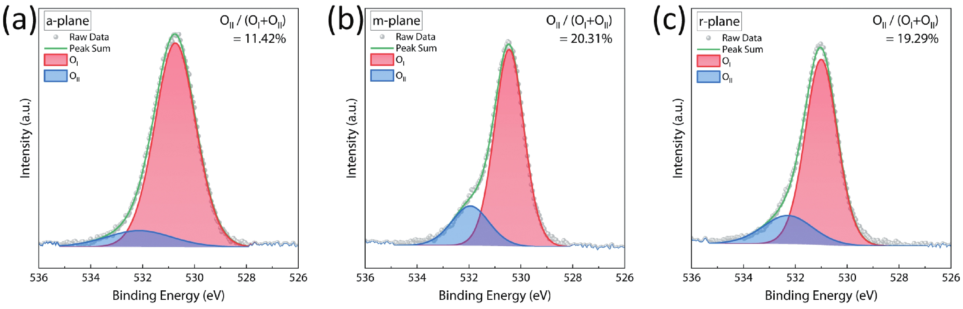
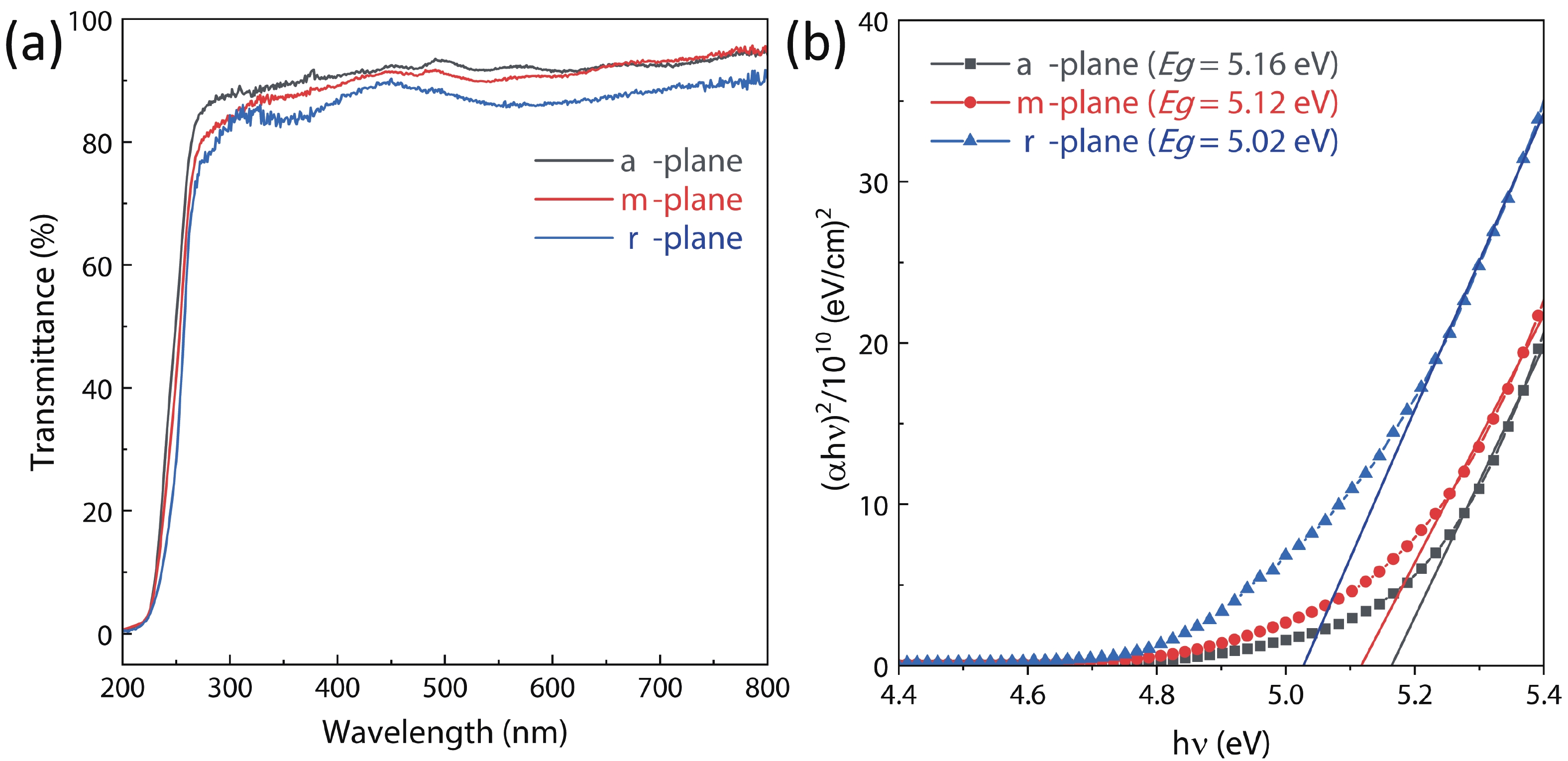
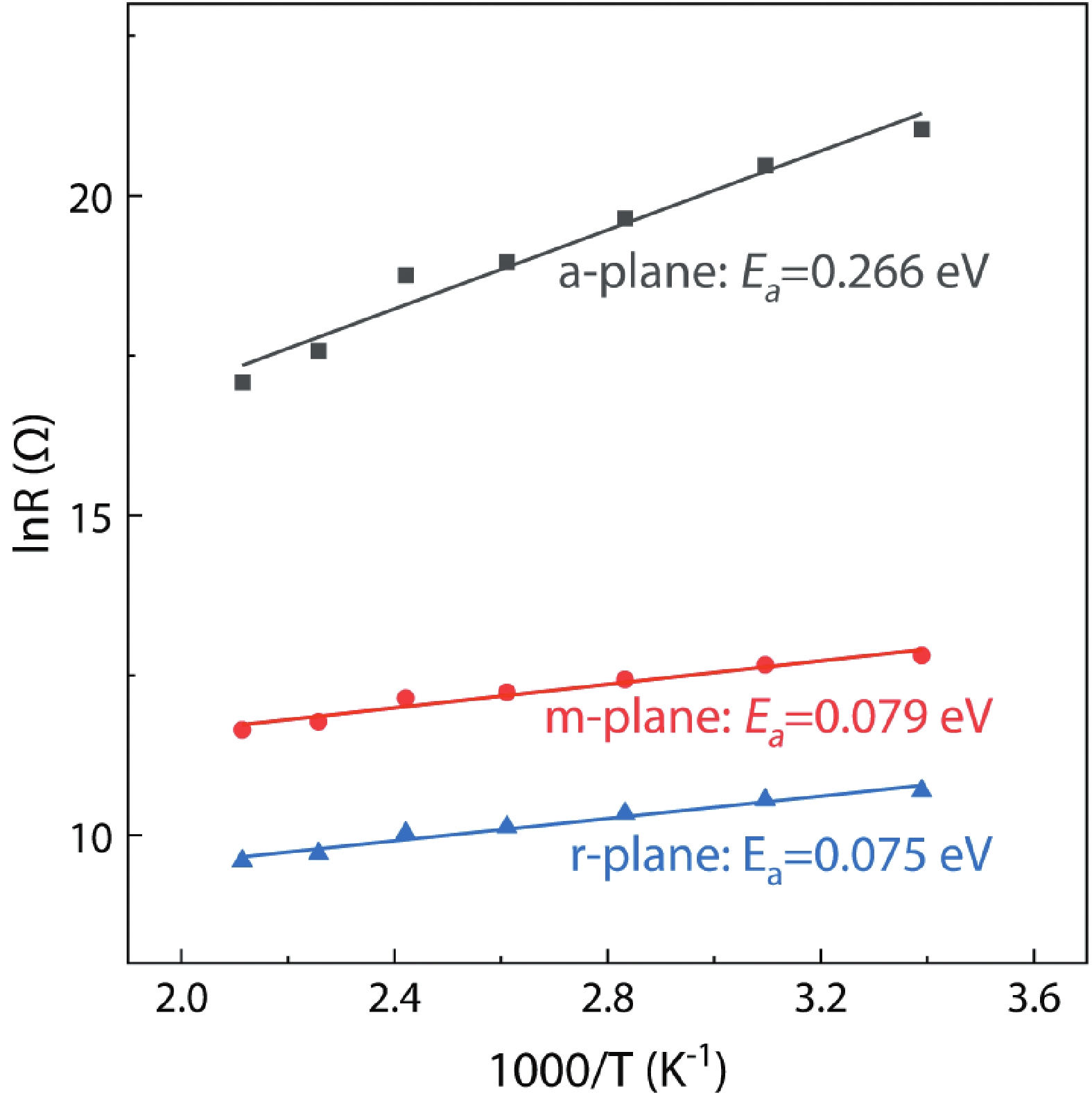
Table 1. Film thicknesses, conductivities, mobilities, and carrier concentrations for α-Ga2O3 thin films grown on a-, c- and r-plane sapphire substrates.
| Substrate | Thickness (nm) | σ (S/cm) | μ (cm2/(V·s)) | n (1017 cm−3) |
| a-sapphire | 302 | Exceed test limit (<0.03) | – | – |
| m-sapphire | 280 | 0.29 | 12.2 | 1.45 |
| r-sapphire | 273 | 2.71 | 1.35 | 125 |
 DownLoad: CSV
| [1] |
Konishi K, Goto K, Murakami H, et al. 1-kV vertical Ga2O3 field-plated Schottky barrier diodes. Appl Phys Lett, 2017, 110, 103506 doi: 10.1063/1.4977857
|
| [2] |
Hu Z Z, Zhou H, Feng Q, et al. Field-plated lateral β-Ga2O3 Schottky barrier diode with high reverse blocking voltage of more than 3 kV and high DC power figure-of-merit of 500 MW/cm2. IEEE Electron Device Lett, 2018, 39, 1564 doi: 10.1109/LED.2018.2868444
|
| [3] |
Hao W B, He Q M, Zhou X Z, et al. 2.6 kV NiO/Ga2O3 heterojunction diode with superior high-temperature voltage blocking capability. 2022 IEEE 34th International Symposium on Power Semiconductor Devices and ICs (ISPSD), 2022, 105 doi: 10.1109/ISPSD49238.2022.9813680
|
| [4] |
Gong H H, Chen X H, Xu Y, et al. A 1.86-kV double-layered NiO/β-Ga2O3 vertical p–n heterojunction diode. Appl Phys Lett, 2020, 117, 022104 doi: 10.1063/5.0010052
|
| [5] |
Zhou X Z, Ma Y J, Xu G W, et al. Enhancement-mode β-Ga2O3 U-shaped gate trench vertical MOSFET realized by oxygen annealing. Appl Phys Lett, 2022, 121, 223501 doi: 10.1063/5.0130292
|
| [6] |
Moser N, McCandless J, Crespo A, et al. Ge-doped β-Ga2O3 MOSFETs. IEEE Electron Device Lett, 2017, 38, 775 doi: 10.1109/LED.2017.2697359
|
| [7] |
Jinno R, Chang C S, Onuma T, et al. Crystal orientation dictated epitaxy of ultrawide-bandgap 5.4- to 8.6-eV α-(AlGa)2O3 on m-plane sapphire. Sci Adv, 2021, 7, eabd5891 doi: 10.1126/sciadv.abd5891
|
| [8] |
Kracht M, Karg A, Feneberg M, et al. Anisotropic optical properties of metastable (011-2) α–Ga2O3 grown by plasma-assisted molecular beam epitaxy. Phys Rev Applied, 2018, 10, 024047 doi: 10.1103/PhysRevApplied.10.024047
|
| [9] |
Wu Z Y, Jiang Z X, Song P Y, et al. Nanowire-seeded growth of single-crystalline (010) β-Ga2 O3 nanosheets with high field-effect electron mobility and on/off current ratio. Small, 2019, 15, e1900580 doi: 10.1002/smll.201900580
|
| [10] |
Zhang W R, Zhang J G, Chen L, et al. Non-equilibrium epitaxy of metastable polymorphs of ultrawide-bandgap gallium oxide. Appl Phys Lett, 2022, 120, 072101 doi: 10.1063/5.0078752
|
| [11] |
Zhang J G, Wang W, Wu S M, et al. Exploratory phase stabilization in heteroepitaxial gallium oxide films by pulsed laser deposition. J Alloys Compd, 2023, 935, 168123 doi: 10.1016/j.jallcom.2022.168123
|
| [12] |
Wu C, Guo D Y, Zhang L Y, et al. Systematic investigation of the growth kinetics of β-Ga2O3 epilayer by plasma enhanced chemical vapor deposition. Appl Phys Lett, 2020, 116, 072102 doi: 10.1063/1.5142196
|
| [13] |
Wang W, Yuan Q L, Han D Y, et al. High-temperature deep ultraviolet photodetector based on a crystalline Ga2O3-diamond heterostructure. IEEE Electron Device Lett, 2022, 43, 2121 doi: 10.1109/LED.2022.3214981
|
| [14] |
Zhang Y B, Zheng J, Ma P P, et al. Growth and characterization of β-Ga2O3 thin films grown on off-angled Al2O3 substrates by metal-organic chemical vapor deposition. J Semicond, 2022, 43, 092801 doi: 10.1088/1674-4926/43/9/092801
|
| [15] |
Sun H D, Li K H, Torres Castanedo C G, et al. HCl flow-induced phase change of α-, β-, and ε-Ga2O3 films grown by MOCVD. Cryst Growth Des, 2018, 18, 2370 doi: 10.1021/acs.cgd.7b01791
|
| [16] |
Hou X H, Sun H D, Long S B, et al. Ultrahigh-performance solar-blind photodetector based on α-phase-dominated Ga2O3 film with record low dark current of 81 fA. IEEE Electron Device Lett, 2019, 40, 1483 doi: 10.1109/LED.2019.2932140
|
| [17] |
Nakagomi S, Kokubun Y. Crystal orientation of β-Ga2O3 thin films formed on c-plane and a-plane sapphire substrate. J Cryst Growth, 2012, 349, 12 doi: 10.1016/j.jcrysgro.2012.04.006
|
| [18] |
Chen X H, Ren F F, Gu S L, et al. Review of gallium-oxide-based solar-blind ultraviolet photodetectors. Photon Res, 2019, 7, 381 doi: 10.1364/PRJ.7.000381
|
| [19] |
Marezio M, Remeika J P. Bond lengths in the α-Ga2O3 structure and the high-pressure phase of Ga2− xFe xO3. J Chem Phys, 1967, 46, 1862 doi: 10.1063/1.1840945
|
| [20] |
Nakagomi S, Kaneko S, Kokubun Y. Crystal orientations of β-Ga2O3 thin films formed on m-plane and r-plane sapphire substrates. Phys Status Solidi B, 2015, 252, 612 doi: 10.1002/pssb.201451456
|
| [21] |
Cheng Y L, Xu Y, Li Z, et al. Heteroepitaxial growth of α-Ga2O3 thin films on a-, c- and r-plane sapphire substrates by low-cost mist-CVD method. J Alloys Compd, 2020, 831, 154776 doi: 10.1016/j.jallcom.2020.154776
|
| [22] |
Hu H Z, Wu C, Zhao N, et al. Epitaxial growth and solar-blind photoelectric characteristic of Ga2O3 film on various oriented sapphire substrates by plasma-enhanced chemical vapor deposition. Phys Status Solidi A, 2021, 218, 2100076 doi: 10.1002/pssa.202100076
|
| [23] |
Chikoidze E, Rogers D J, Teherani F H, et al. Puzzling robust 2D metallic conductivity in undoped β-Ga2O3 thin films. Mater Today Phys, 2019, 8, 10 doi: 10.1016/j.mtphys.2018.11.006
|
| [24] |
Ghosh K, Singisetti U. Electron mobility in monoclinic β-Ga2O3—Effect of plasmon-phonon coupling, anisotropy, and confinement. J Mater Res, 2017, 32, 4142 doi: 10.1557/jmr.2017.398
|
| [25] |
Hou X, Zhao X, Zhang Y, et al. High-performance harsh-environment-resistant GaOX solar-blind photodetectors via defect and doping engineering. Adv Mater, 2022, 34, e2106923 doi: 10.1002/adma.202106923
|
| [26] |
Zhang T, Guan D G, Liu N T, et al. Room temperature fabrication and post-annealing treatment of amorphous Ga2O3 photodetectors for deep-ultraviolet light detection. Appl Phys Express, 2022, 15, 022007 doi: 10.35848/1882-0786/ac48d9
|
| [27] |
Xiang X Q, Li L H, Chen C, et al. Unintentional doping effect in Si-doped MOCVD β-Ga2O3 films: Shallow donor states. Sci China Mater, 2023, 66, 748 doi: 10.1007/s40843-022-2167-x
|
| [28] |
Qin Y, Li L H, Zhao X L, et al. Metal–semiconductor–metal ε-Ga2O3 solar-blind photodetectors with a record-high responsivity rejection ratio and their gain mechanism. ACS Photonics, 2020, 7, 812 doi: 10.1021/acsphotonics.9b01727
|
| [29] |
Waseem A, Ren Z J, Huang H C, et al. A review of recent progress in β-Ga2O3 epitaxial growth: Effect of substrate orientation and precursors in metal–organic chemical vapor deposition. Phys Status Solidi A, 2022, 2200616 doi: 10.1002/pssa.202200616
|
| [30] |
Liu N T, Zhang T, Chen L, et al. Fast-response amorphous Ga2O3 solar-blind ultraviolet photodetectors tuned by a polar AlN template. IEEE Electron Device Lett, 2022, 43, 68 doi: 10.1109/LED.2021.3132497
|
| [31] |
Cuscó R, Domènech-Amador N, Hatakeyama T, et al. Lattice dynamics of a mist-chemical vapor deposition-grown corundum-like Ga2O3 single crystal. J Appl Phys, 2015, 117, 185706 doi: 10.1063/1.4921060
|
| [32] |
Ma T C, Chen X H, Ren F F, et al. Heteroepitaxial growth of thick α-Ga2O3 film on sapphire (0001) by MIST-CVD technique. J Semicond, 2019, 40, 012804 doi: 10.1088/1674-4926/40/1/012804
|
| [33] |
Mazzolini P, Falkenstein A, Wouters C, et al. Substrate-orientation dependence of β-Ga2O3 (100), (010), (001), and (-201) homoepitaxy by indium-mediated metal-exchange catalyzed molecular beam epitaxy (MEXCAT-MBE). APL Mater, 2020, 8, 011107 doi: 10.1063/1.5135772
|
| [34] |
Yen C C, Huang T M, Chen P W, et al. Role of interfacial oxide in the preferred orientation of Ga2O3 on Si for deep ultraviolet photodetectors. ACS Omega, 2021, 6, 29149 doi: 10.1021/acsomega.1c04380
|
| [35] |
Tak B R, Dewan S, Goyal A, et al. Point defects induced work function modulation of β-Ga2O3. Appl Surf Sci, 2019, 465, 973 doi: 10.1016/j.apsusc.2018.09.236
|
| [36] |
Miller A, Abrahams E. Impurity conduction at low concentrations. Phys Rev, 1960, 120, 745 doi: 10.1103/PhysRev.120.745
|
| [37] |
Hajnal Z, Miró J, Kiss G, et al. Role of oxygen vacancy defect states in the n-type conduction of β-Ga2O3. J Appl Phys, 1999, 86, 3792 doi: 10.1063/1.371289
|
| [38] |
Zhang J Y, Shi J L, Qi D C, et al. Recent progress on the electronic structure, defect, and doping properties of Ga2O3. APL Mater, 2020, 8, 020906 doi: 10.1063/1.5142999
|


Article views: 1281 Times PDF downloads: 195 Times Cited by: 0 Times
Received: 28 December 2022 Revised: 03 February 2023 Online: Accepted Manuscript: 10 March 2023Uncorrected proof: 12 April 2023Corrected proof: 22 May 2023Published: 08 June 2023
| Citation: |
Wei Wang, Shudong Hu, Zilong Wang, Kaisen Liu, Jinfu Zhang, Simiao Wu, Yuxia Yang, Ning Xia, Wenrui Zhang, Jichun Ye. Exploring heteroepitaxial growth and electrical properties of α-Ga2O3 films on differently oriented sapphire substrates[J]. Journal of Semiconductors, 2023, 44(6): 062802. doi: 10.1088/1674-4926/44/6/062802
W Wang, S D Hu, Z L Wang, K S Liu, J F Zhang, S M Wu, Y X Yang, N Xia, W R Zhang, J C Ye. Exploring heteroepitaxial growth and electrical properties of α-Ga2O3 films on differently oriented sapphire substrates[J]. J. Semicond, 2023, 44(6): 062802. doi: 10.1088/1674-4926/44/6/062802
Export: BibTex EndNote

|
| [1] |
Konishi K, Goto K, Murakami H, et al. 1-kV vertical Ga2O3 field-plated Schottky barrier diodes. Appl Phys Lett, 2017, 110, 103506 doi: 10.1063/1.4977857
|
| [2] |
Hu Z Z, Zhou H, Feng Q, et al. Field-plated lateral β-Ga2O3 Schottky barrier diode with high reverse blocking voltage of more than 3 kV and high DC power figure-of-merit of 500 MW/cm2. IEEE Electron Device Lett, 2018, 39, 1564 doi: 10.1109/LED.2018.2868444
|
| [3] |
Hao W B, He Q M, Zhou X Z, et al. 2.6 kV NiO/Ga2O3 heterojunction diode with superior high-temperature voltage blocking capability. 2022 IEEE 34th International Symposium on Power Semiconductor Devices and ICs (ISPSD), 2022, 105 doi: 10.1109/ISPSD49238.2022.9813680
|
| [4] |
Gong H H, Chen X H, Xu Y, et al. A 1.86-kV double-layered NiO/β-Ga2O3 vertical p–n heterojunction diode. Appl Phys Lett, 2020, 117, 022104 doi: 10.1063/5.0010052
|
| [5] |
Zhou X Z, Ma Y J, Xu G W, et al. Enhancement-mode β-Ga2O3 U-shaped gate trench vertical MOSFET realized by oxygen annealing. Appl Phys Lett, 2022, 121, 223501 doi: 10.1063/5.0130292
|
| [6] |
Moser N, McCandless J, Crespo A, et al. Ge-doped β-Ga2O3 MOSFETs. IEEE Electron Device Lett, 2017, 38, 775 doi: 10.1109/LED.2017.2697359
|
| [7] |
Jinno R, Chang C S, Onuma T, et al. Crystal orientation dictated epitaxy of ultrawide-bandgap 5.4- to 8.6-eV α-(AlGa)2O3 on m-plane sapphire. Sci Adv, 2021, 7, eabd5891 doi: 10.1126/sciadv.abd5891
|
| [8] |
Kracht M, Karg A, Feneberg M, et al. Anisotropic optical properties of metastable (011-2) α–Ga2O3 grown by plasma-assisted molecular beam epitaxy. Phys Rev Applied, 2018, 10, 024047 doi: 10.1103/PhysRevApplied.10.024047
|
| [9] |
Wu Z Y, Jiang Z X, Song P Y, et al. Nanowire-seeded growth of single-crystalline (010) β-Ga2 O3 nanosheets with high field-effect electron mobility and on/off current ratio. Small, 2019, 15, e1900580 doi: 10.1002/smll.201900580
|
| [10] |
Zhang W R, Zhang J G, Chen L, et al. Non-equilibrium epitaxy of metastable polymorphs of ultrawide-bandgap gallium oxide. Appl Phys Lett, 2022, 120, 072101 doi: 10.1063/5.0078752
|
| [11] |
Zhang J G, Wang W, Wu S M, et al. Exploratory phase stabilization in heteroepitaxial gallium oxide films by pulsed laser deposition. J Alloys Compd, 2023, 935, 168123 doi: 10.1016/j.jallcom.2022.168123
|
| [12] |
Wu C, Guo D Y, Zhang L Y, et al. Systematic investigation of the growth kinetics of β-Ga2O3 epilayer by plasma enhanced chemical vapor deposition. Appl Phys Lett, 2020, 116, 072102 doi: 10.1063/1.5142196
|
| [13] |
Wang W, Yuan Q L, Han D Y, et al. High-temperature deep ultraviolet photodetector based on a crystalline Ga2O3-diamond heterostructure. IEEE Electron Device Lett, 2022, 43, 2121 doi: 10.1109/LED.2022.3214981
|
| [14] |
Zhang Y B, Zheng J, Ma P P, et al. Growth and characterization of β-Ga2O3 thin films grown on off-angled Al2O3 substrates by metal-organic chemical vapor deposition. J Semicond, 2022, 43, 092801 doi: 10.1088/1674-4926/43/9/092801
|
| [15] |
Sun H D, Li K H, Torres Castanedo C G, et al. HCl flow-induced phase change of α-, β-, and ε-Ga2O3 films grown by MOCVD. Cryst Growth Des, 2018, 18, 2370 doi: 10.1021/acs.cgd.7b01791
|
| [16] |
Hou X H, Sun H D, Long S B, et al. Ultrahigh-performance solar-blind photodetector based on α-phase-dominated Ga2O3 film with record low dark current of 81 fA. IEEE Electron Device Lett, 2019, 40, 1483 doi: 10.1109/LED.2019.2932140
|
| [17] |
Nakagomi S, Kokubun Y. Crystal orientation of β-Ga2O3 thin films formed on c-plane and a-plane sapphire substrate. J Cryst Growth, 2012, 349, 12 doi: 10.1016/j.jcrysgro.2012.04.006
|
| [18] |
Chen X H, Ren F F, Gu S L, et al. Review of gallium-oxide-based solar-blind ultraviolet photodetectors. Photon Res, 2019, 7, 381 doi: 10.1364/PRJ.7.000381
|
| [19] |
Marezio M, Remeika J P. Bond lengths in the α-Ga2O3 structure and the high-pressure phase of Ga2− xFe xO3. J Chem Phys, 1967, 46, 1862 doi: 10.1063/1.1840945
|
| [20] |
Nakagomi S, Kaneko S, Kokubun Y. Crystal orientations of β-Ga2O3 thin films formed on m-plane and r-plane sapphire substrates. Phys Status Solidi B, 2015, 252, 612 doi: 10.1002/pssb.201451456
|
| [21] |
Cheng Y L, Xu Y, Li Z, et al. Heteroepitaxial growth of α-Ga2O3 thin films on a-, c- and r-plane sapphire substrates by low-cost mist-CVD method. J Alloys Compd, 2020, 831, 154776 doi: 10.1016/j.jallcom.2020.154776
|
| [22] |
Hu H Z, Wu C, Zhao N, et al. Epitaxial growth and solar-blind photoelectric characteristic of Ga2O3 film on various oriented sapphire substrates by plasma-enhanced chemical vapor deposition. Phys Status Solidi A, 2021, 218, 2100076 doi: 10.1002/pssa.202100076
|
| [23] |
Chikoidze E, Rogers D J, Teherani F H, et al. Puzzling robust 2D metallic conductivity in undoped β-Ga2O3 thin films. Mater Today Phys, 2019, 8, 10 doi: 10.1016/j.mtphys.2018.11.006
|
| [24] |
Ghosh K, Singisetti U. Electron mobility in monoclinic β-Ga2O3—Effect of plasmon-phonon coupling, anisotropy, and confinement. J Mater Res, 2017, 32, 4142 doi: 10.1557/jmr.2017.398
|
| [25] |
Hou X, Zhao X, Zhang Y, et al. High-performance harsh-environment-resistant GaOX solar-blind photodetectors via defect and doping engineering. Adv Mater, 2022, 34, e2106923 doi: 10.1002/adma.202106923
|
| [26] |
Zhang T, Guan D G, Liu N T, et al. Room temperature fabrication and post-annealing treatment of amorphous Ga2O3 photodetectors for deep-ultraviolet light detection. Appl Phys Express, 2022, 15, 022007 doi: 10.35848/1882-0786/ac48d9
|
| [27] |
Xiang X Q, Li L H, Chen C, et al. Unintentional doping effect in Si-doped MOCVD β-Ga2O3 films: Shallow donor states. Sci China Mater, 2023, 66, 748 doi: 10.1007/s40843-022-2167-x
|
| [28] |
Qin Y, Li L H, Zhao X L, et al. Metal–semiconductor–metal ε-Ga2O3 solar-blind photodetectors with a record-high responsivity rejection ratio and their gain mechanism. ACS Photonics, 2020, 7, 812 doi: 10.1021/acsphotonics.9b01727
|
| [29] |
Waseem A, Ren Z J, Huang H C, et al. A review of recent progress in β-Ga2O3 epitaxial growth: Effect of substrate orientation and precursors in metal–organic chemical vapor deposition. Phys Status Solidi A, 2022, 2200616 doi: 10.1002/pssa.202200616
|
| [30] |
Liu N T, Zhang T, Chen L, et al. Fast-response amorphous Ga2O3 solar-blind ultraviolet photodetectors tuned by a polar AlN template. IEEE Electron Device Lett, 2022, 43, 68 doi: 10.1109/LED.2021.3132497
|
| [31] |
Cuscó R, Domènech-Amador N, Hatakeyama T, et al. Lattice dynamics of a mist-chemical vapor deposition-grown corundum-like Ga2O3 single crystal. J Appl Phys, 2015, 117, 185706 doi: 10.1063/1.4921060
|
| [32] |
Ma T C, Chen X H, Ren F F, et al. Heteroepitaxial growth of thick α-Ga2O3 film on sapphire (0001) by MIST-CVD technique. J Semicond, 2019, 40, 012804 doi: 10.1088/1674-4926/40/1/012804
|
| [33] |
Mazzolini P, Falkenstein A, Wouters C, et al. Substrate-orientation dependence of β-Ga2O3 (100), (010), (001), and (-201) homoepitaxy by indium-mediated metal-exchange catalyzed molecular beam epitaxy (MEXCAT-MBE). APL Mater, 2020, 8, 011107 doi: 10.1063/1.5135772
|
| [34] |
Yen C C, Huang T M, Chen P W, et al. Role of interfacial oxide in the preferred orientation of Ga2O3 on Si for deep ultraviolet photodetectors. ACS Omega, 2021, 6, 29149 doi: 10.1021/acsomega.1c04380
|
| [35] |
Tak B R, Dewan S, Goyal A, et al. Point defects induced work function modulation of β-Ga2O3. Appl Surf Sci, 2019, 465, 973 doi: 10.1016/j.apsusc.2018.09.236
|
| [36] |
Miller A, Abrahams E. Impurity conduction at low concentrations. Phys Rev, 1960, 120, 745 doi: 10.1103/PhysRev.120.745
|
| [37] |
Hajnal Z, Miró J, Kiss G, et al. Role of oxygen vacancy defect states in the n-type conduction of β-Ga2O3. J Appl Phys, 1999, 86, 3792 doi: 10.1063/1.371289
|
| [38] |
Zhang J Y, Shi J L, Qi D C, et al. Recent progress on the electronic structure, defect, and doping properties of Ga2O3. APL Mater, 2020, 8, 020906 doi: 10.1063/1.5142999
|

 WeChat ID
Journal of Semiconductors © 2017 All Rights Reserved 京ICP备05085259号-2


