


Fig. 1.
The simplified layout of the MOSFETs.
SEMICONDUCTOR DEVICES
Jianhui Bu, Shuzhen Li, Jiajun Luo and Zhengsheng Han
Corresponding author: Bu Jianhui, Email:bujianhui@ime.ac.cn
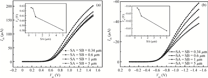
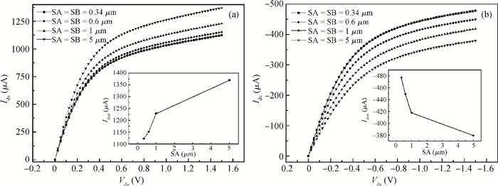
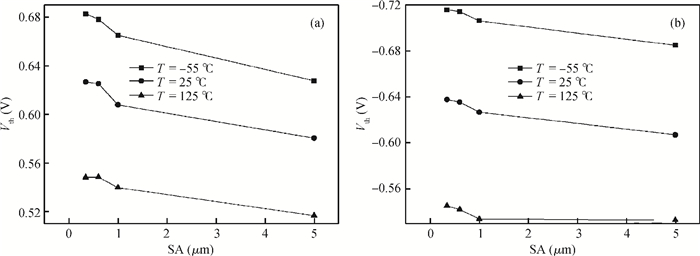
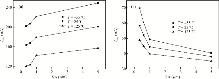
Abstract: The STI stress effect is investigated based on the 0.13 μm SOI process developed by the Institute of Microelectronics of the Chinese Academy of Sciences (IMECAS). It shows that the threshold voltage and mobility are all affected by the STI stress. The absolute value of the threshold voltage of NMOS and PMOS increased by about 10%, the saturation current of NMOS decreases by about 20%, while the saturation current of PMOS increases by about 20%. It is also found that the lower temperature enhances the STI stress and then influences the device performance further. Then a macro model for this effect is proposed and is well verified.
Key words: PDSOI, STI stress, temperature, model
| [1] |
Tan P B Y, Kordesch A V, Sidek O. Compact modeling of mechanical STI y-stress effect. IEEE International Conference on Solid-State and Integrated Circuit Technology, 2006:1450 http://ieeexplore.ieee.org/document/4098437/
|
| [2] |
Tan P B Y, Kordesch A V, Sidek O. Physical-based SPICE model of CMOS STI y-stress effect. IEEE International Conference on Semiconductor Electronics, 2006:755 http://ieeexplore.ieee.org/document/4266720/
|
| [3] |
Yeh K L, Guo J C. Layout-dependent stress effect on high-frequency characteristics and flicker noise in multifinger and donut MOSFETs. IEEE Trans Electron Devices, 2011, 58(9):3140 doi: 10.1109/TED.2011.2159223
|
| [4] |
Wu W, Du G, Liu X, et al. Physical-based threshold voltage and mobility models including shallow trench isolation stress effect on nMOSFETs. IEEE Trans Nanotechnology, 2011, 10(4):875 doi: 10.1109/TNANO.2010.2089468
|
| [5] |
Wu Wei, Du Gang, Liu Xiaoyan, et al. A physical-based pMOSFETs threshold voltage model including the STI stress effect. Journal of smiconductors, 2011, 32(5):054005 doi: 10.1088/1674-4926/32/5/054005
|
| [6] |
Jiang H, Yap H K, Pandey S M, et al. Impact of STI stress on hot carrier degradation in 5 V NMOSFET. IEEE International Integrated Reliability Workshop Final Report (IRW), 2011:94
|
| [7] |
BSIMSOIv4. 4 MOSFET MODEL Users' Manual. 2010: 54
|
| [8] |
Tan P B Y, Kordesch A V, Sidek O. Analysis of deep submicron CMOS transistor Vtlin and Idsat versus channel width. Asia-Pacific Microwave Conference (APMC), 2005:1569
|


Article views: 3818 Times PDF downloads: 35 Times Cited by: 0 Times
Received: 11 August 2013 Revised: 09 October 2013 Online: Published: 01 March 2014
| Citation: |
Jianhui Bu, Shuzhen Li, Jiajun Luo, Zhengsheng Han. The STI stress effect on deep submicron PDSOI MOSFETs[J]. Journal of Semiconductors, 2014, 35(3): 034008. doi: 10.1088/1674-4926/35/3/034008
J H Bu, S Z Li, J J Luo, Z S Han. The STI stress effect on deep submicron PDSOI MOSFETs[J]. J. Semicond., 2014, 35(3): 034008. doi: 10.1088/1674-4926/35/3/034008.
Export: BibTex EndNote

|
| [1] |
Tan P B Y, Kordesch A V, Sidek O. Compact modeling of mechanical STI y-stress effect. IEEE International Conference on Solid-State and Integrated Circuit Technology, 2006:1450 http://ieeexplore.ieee.org/document/4098437/
|
| [2] |
Tan P B Y, Kordesch A V, Sidek O. Physical-based SPICE model of CMOS STI y-stress effect. IEEE International Conference on Semiconductor Electronics, 2006:755 http://ieeexplore.ieee.org/document/4266720/
|
| [3] |
Yeh K L, Guo J C. Layout-dependent stress effect on high-frequency characteristics and flicker noise in multifinger and donut MOSFETs. IEEE Trans Electron Devices, 2011, 58(9):3140 doi: 10.1109/TED.2011.2159223
|
| [4] |
Wu W, Du G, Liu X, et al. Physical-based threshold voltage and mobility models including shallow trench isolation stress effect on nMOSFETs. IEEE Trans Nanotechnology, 2011, 10(4):875 doi: 10.1109/TNANO.2010.2089468
|
| [5] |
Wu Wei, Du Gang, Liu Xiaoyan, et al. A physical-based pMOSFETs threshold voltage model including the STI stress effect. Journal of smiconductors, 2011, 32(5):054005 doi: 10.1088/1674-4926/32/5/054005
|
| [6] |
Jiang H, Yap H K, Pandey S M, et al. Impact of STI stress on hot carrier degradation in 5 V NMOSFET. IEEE International Integrated Reliability Workshop Final Report (IRW), 2011:94
|
| [7] |
BSIMSOIv4. 4 MOSFET MODEL Users' Manual. 2010: 54
|
| [8] |
Tan P B Y, Kordesch A V, Sidek O. Analysis of deep submicron CMOS transistor Vtlin and Idsat versus channel width. Asia-Pacific Microwave Conference (APMC), 2005:1569
|

 WeChat ID
Journal of Semiconductors © 2017 All Rights Reserved 京ICP备05085259号-2

 DownLoad:

