Issue Browser
Volume 40, Issue 4,
Apr 2019

J. Semicond.
2019, 40(4): 041901 doi: 10.1088/1674-4926/40/4/041901
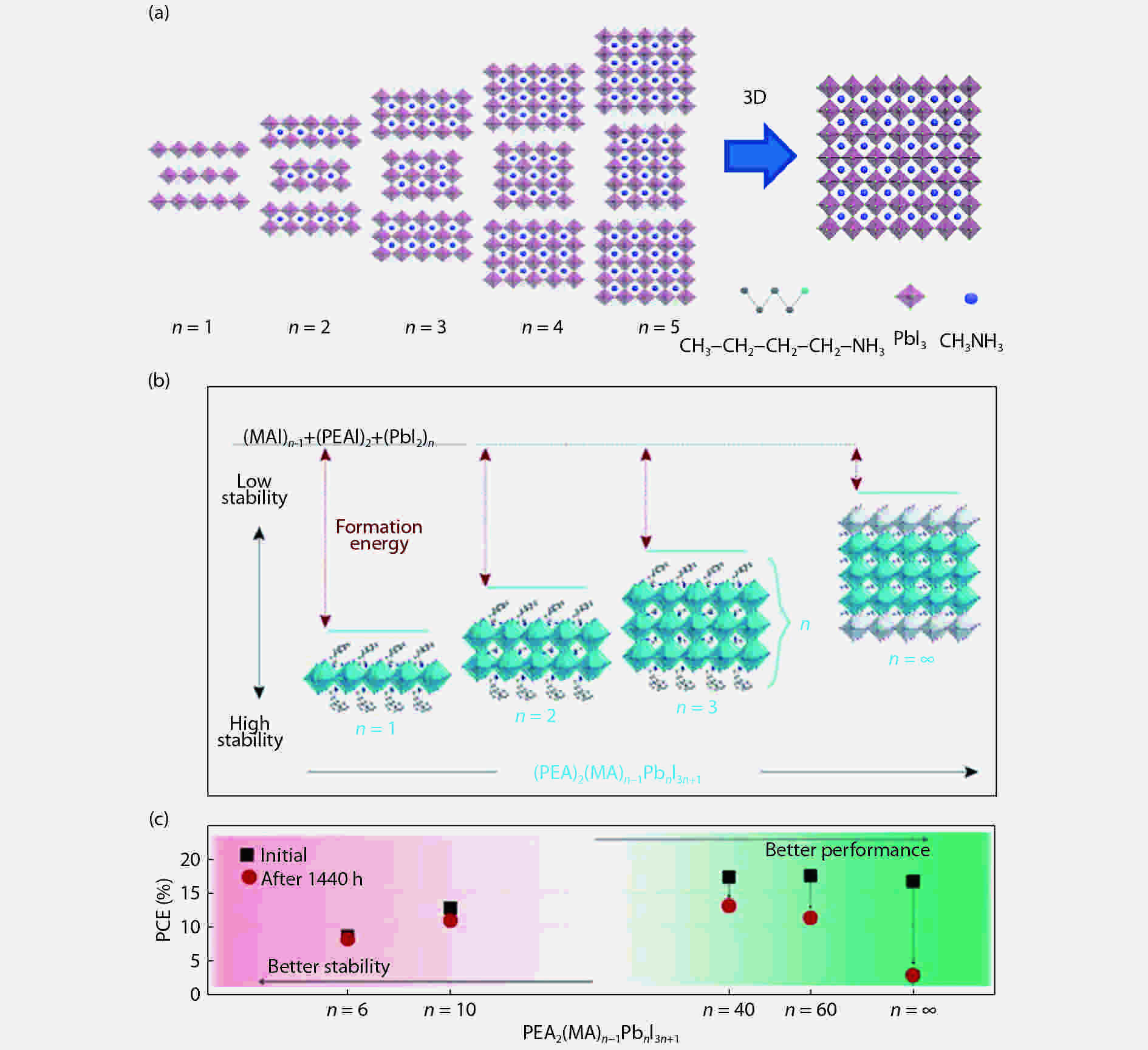
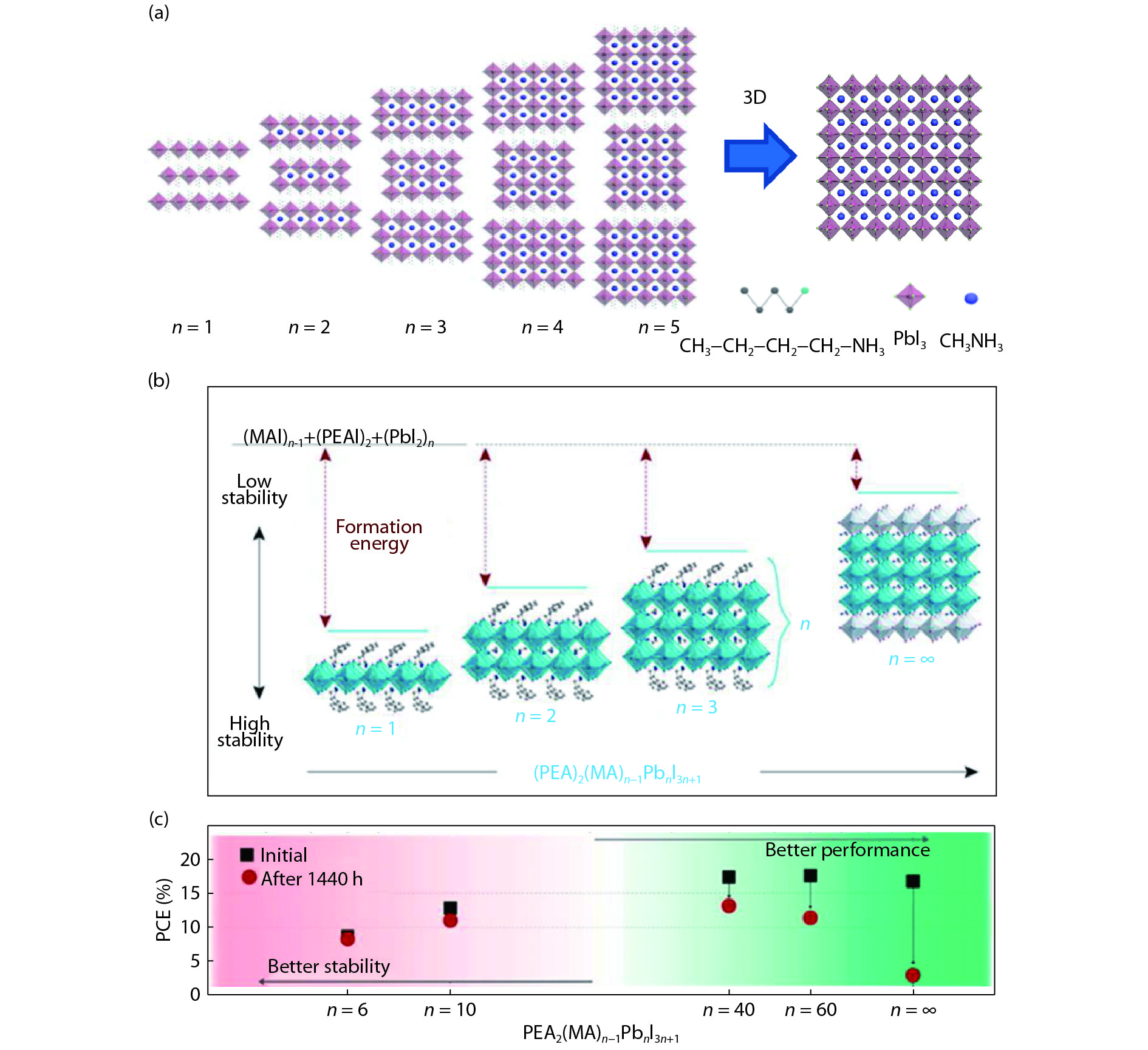
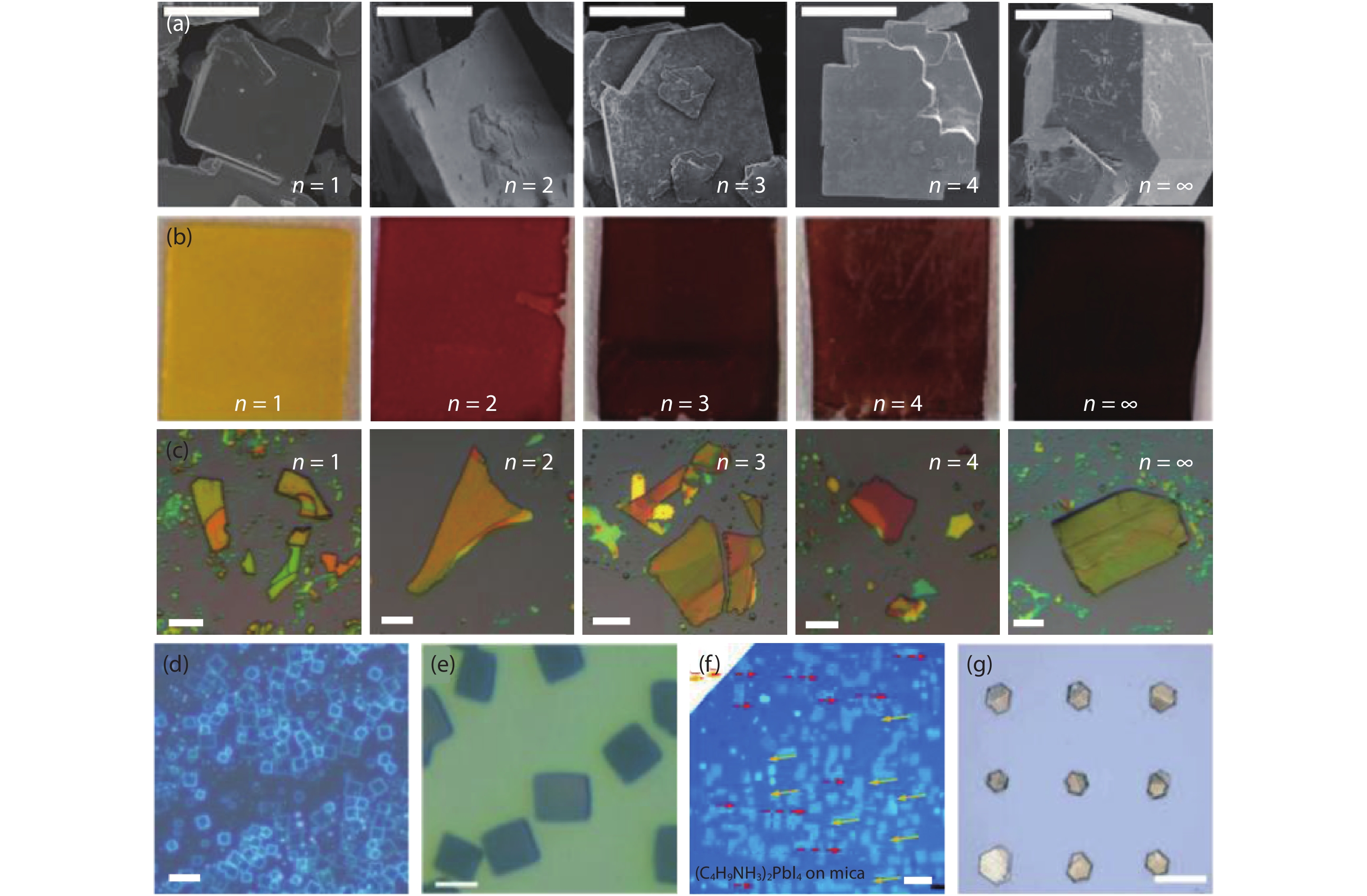
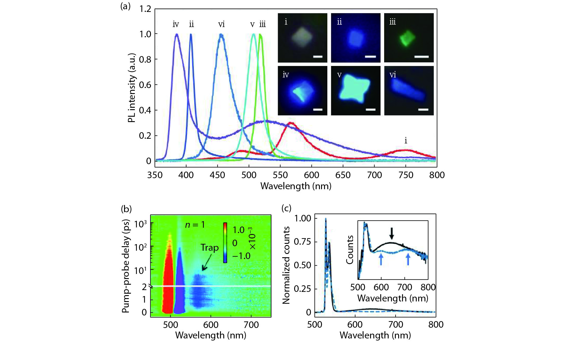
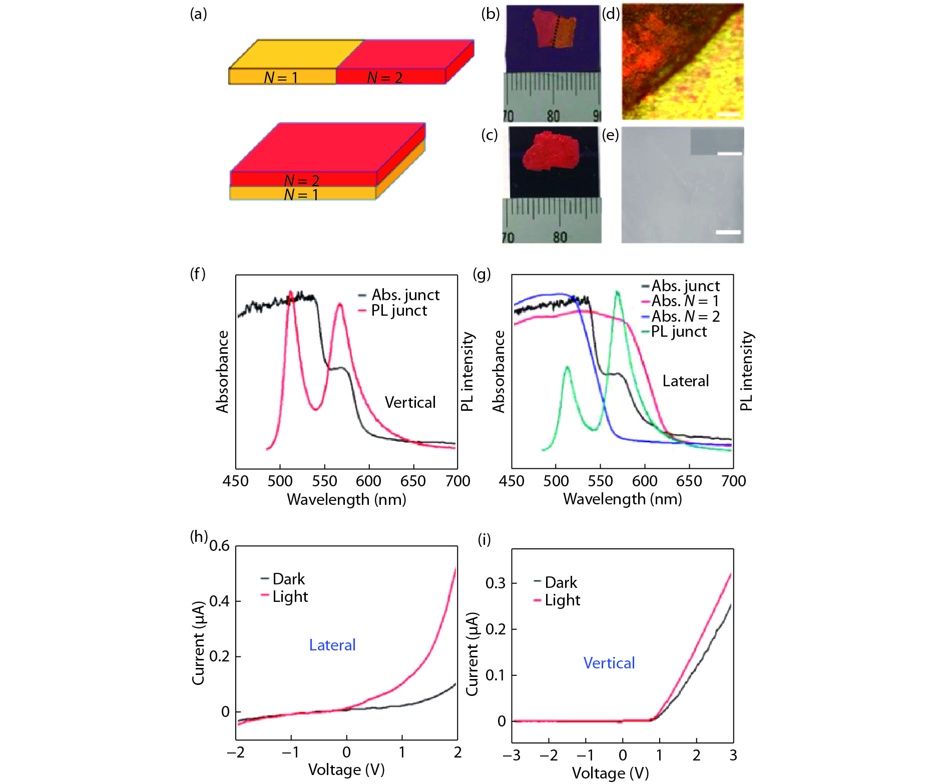
Two-dimensional (2D) hybrid organic-inorganic perovskites have recently attracted attention due to their layered nature, naturally formed quantum well structure, large exciton binding energy and especially better long-term environmental stability compared with their three-dimensional (3D) counterparts. In this report, we present a brief overview of the recent progress of the optoelectronic applications in 2D perovskites. The layer number dependent physical properties of 2D perovskites will first be introduced and then the different synthetic approaches to achieve 2D perovskites with different morphologies will be discussed. The optical, optoelectronic properties and self-trapped states in 2D perovskites will be described, which are indispensable for designing the new device structures with novel functionalities and improving the device performance. Subsequently, a brief summary of the advantages and the current research status of the 2D perovskite-based heterostructures will be illustrated. Finally, a perspective of 2D perovskite materials is given toward their material synthesis and novel device applications.
J. Semicond.
2019, 40(4): 042101 doi: 10.1088/1674-4926/40/4/042101
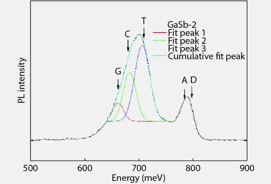
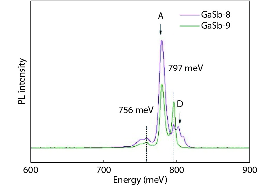
Lightly Te-doped GaSb samples grown by the liquid encapsulated Czochralski (LEC) method have been studied by Hall measurements and low-temperature PL spectroscopy. The results suggest that acceptor-related antisite is the dominant defect in n-type GaSb with low Te-doping concentration. As the Te concentration increases, gallium vacancy related defects become the main acceptor. A new band of around 665 meV is observed in the GaSb sample with the lowest Te-doping concentration. The variation of the acceptor defects and their influence on the electronic and optical property on the n-GaSb single crystal are discussed based on the results.


J. Semicond.
2019, 40(4): 042102 doi: 10.1088/1674-4926/40/4/042102

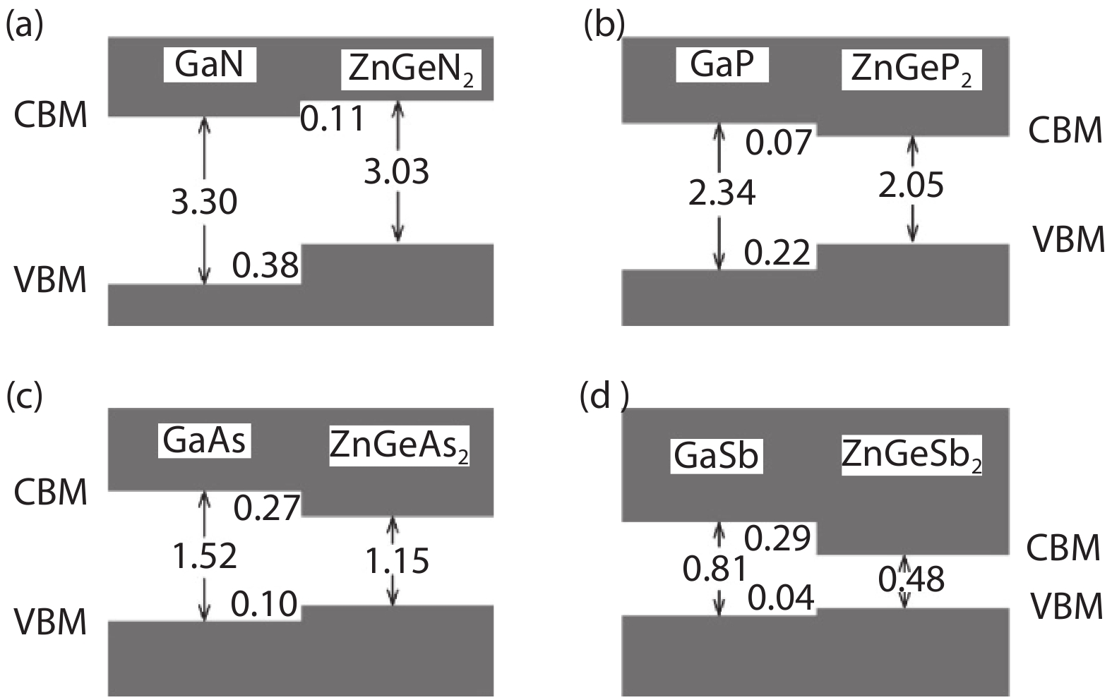
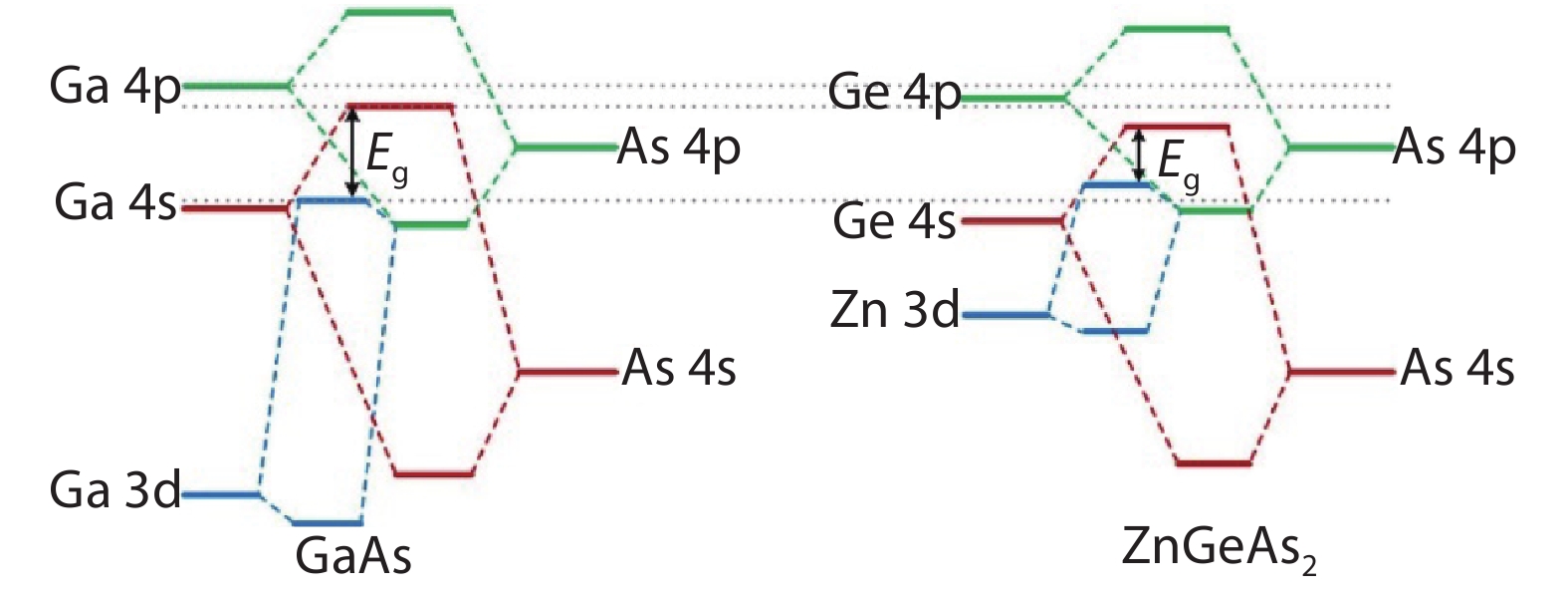
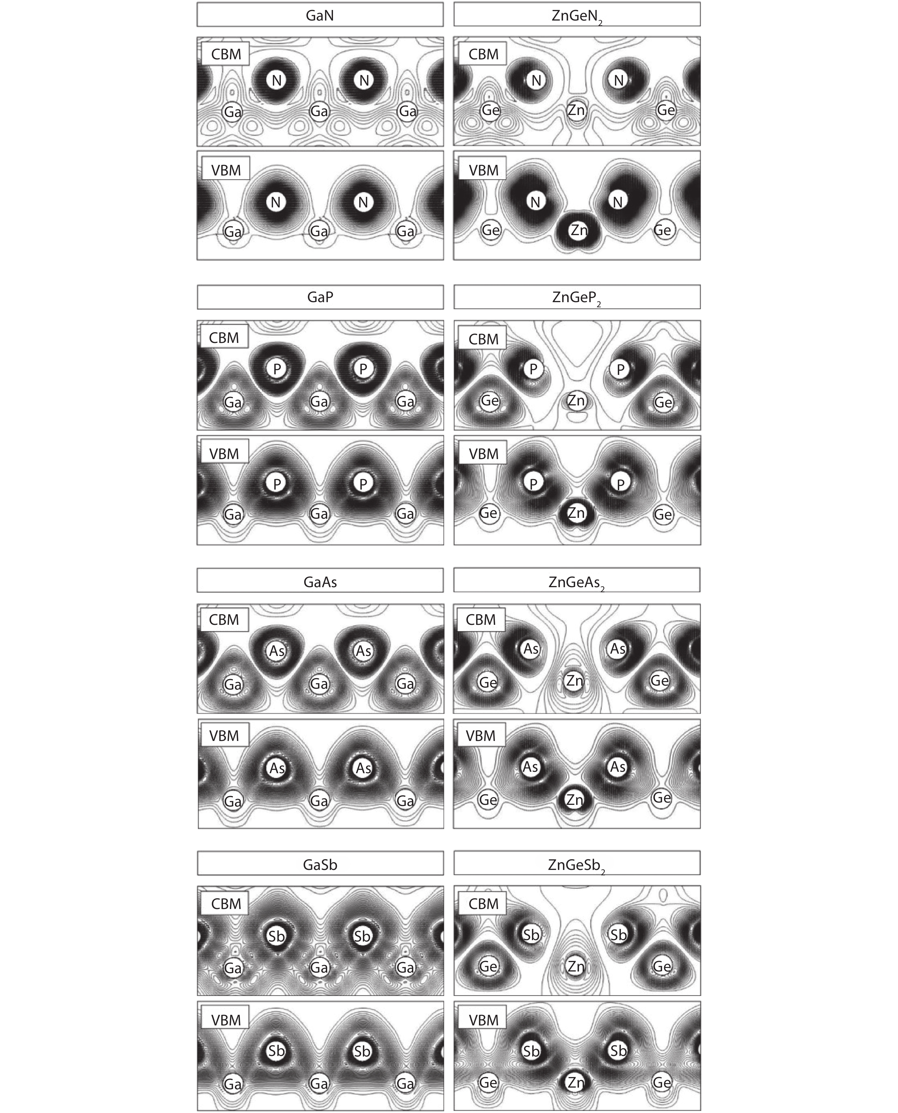
Utilizing first-principles band structure method, we studied the trends of electronic structures and band offsets of the common-anion heterojunctions GaX/ZnGeX2 (X = N, P, As, Sb). Here, ZnGeX2 can be derived by atomic transmutation of two Ga atoms in GaX into one Zn atom and one Ge atom. The calculated results show that the valence band maximums (VBMs) of GaX are always lower in energy than that of ZnGeX2, and the band offset decreases when the anion atomic number increases. The conduction band minimums (CBMs) of ZnGeX2 are lower than that of GaX for X = P, As, and Sb, as expected. However, surprisingly, for ZnGeN2, its CBM is higher than GaN. We found that the coupling between anion p and cation d states plays a decisive role in determining the position of the valence band maximum, and the increased electronegativity of Ge relative to Ga explains the lower CBMs of ZnGeX2 for X = P, As, and Sb. Meanwhile, due to the high ionicity, the strong coulomb interaction is the origin of the anomalous behavior for nitrides.

J. Semicond.
2019, 40(4): 042401 doi: 10.1088/1674-4926/40/4/042401
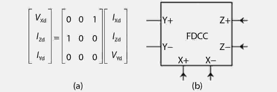
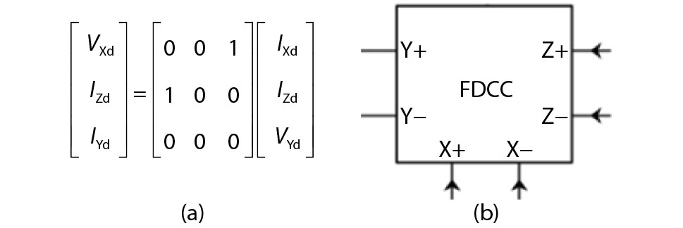
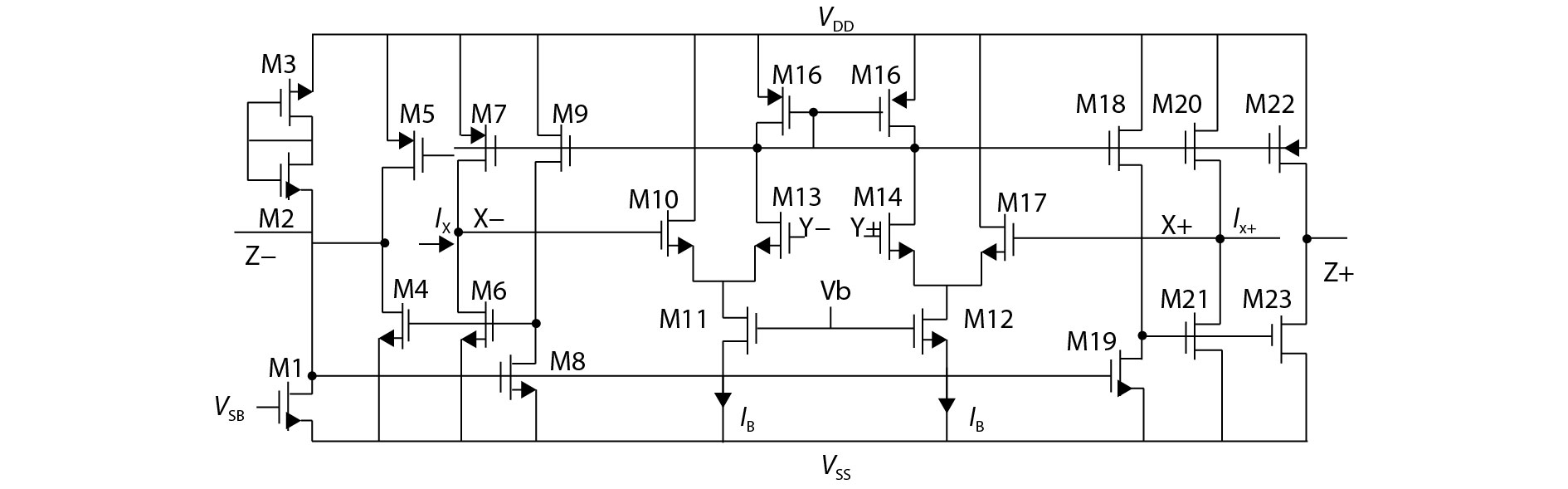
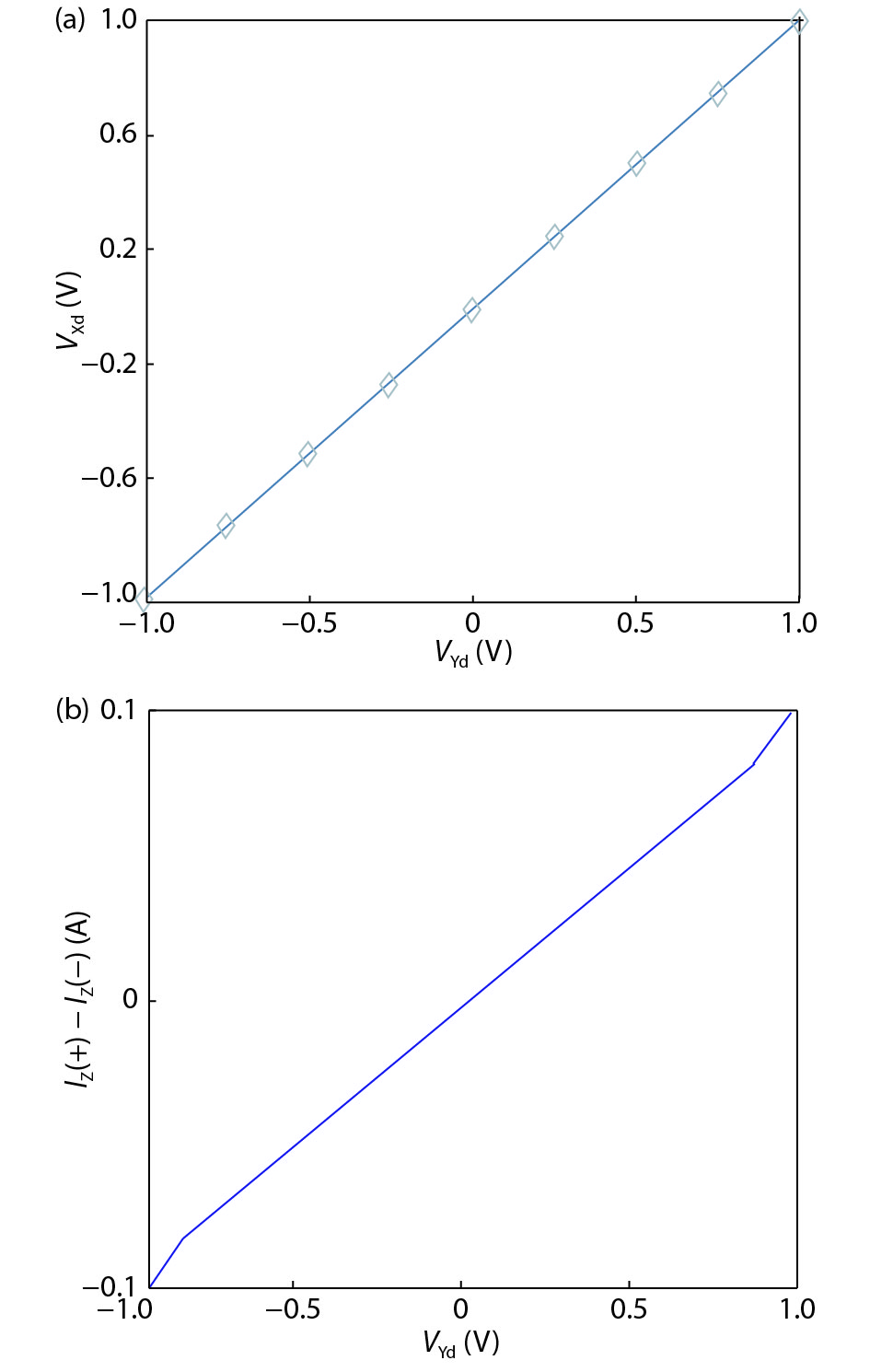
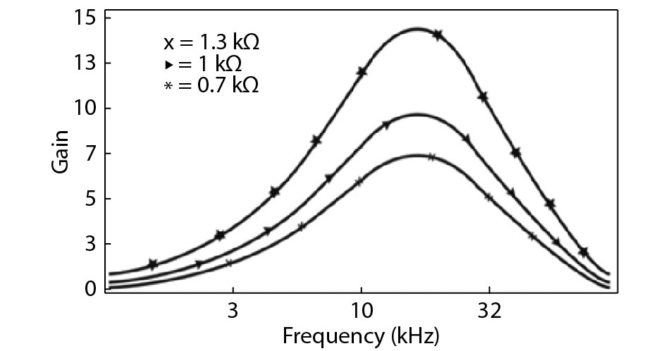
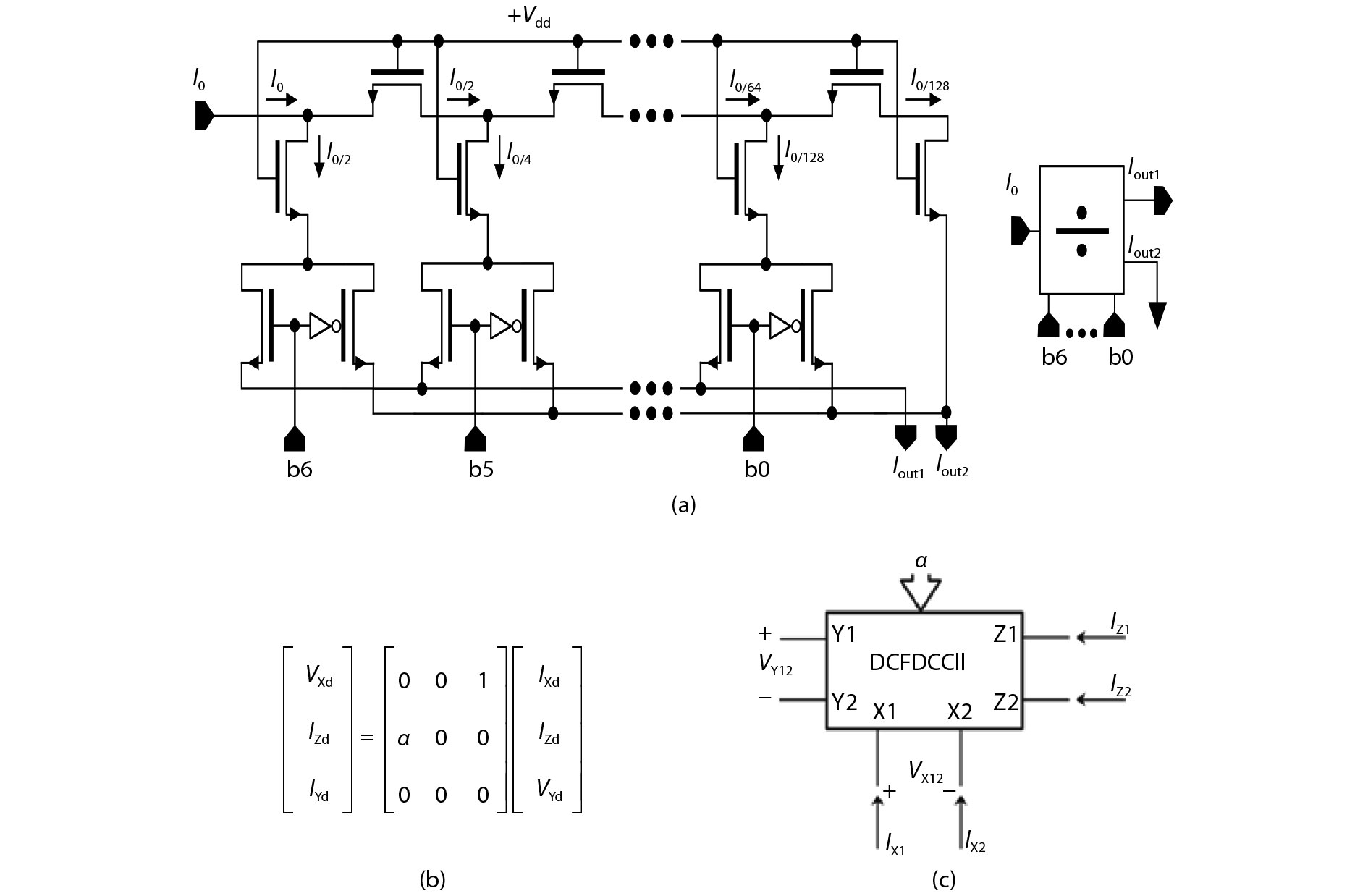
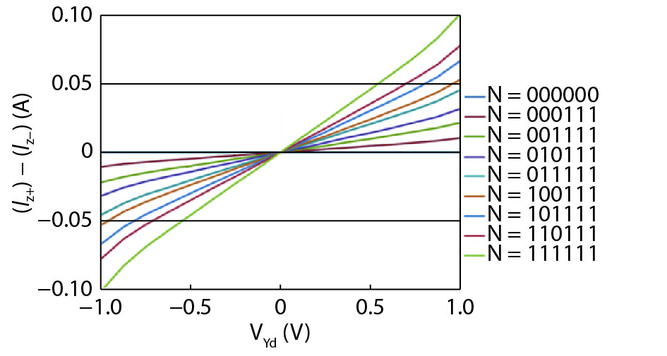
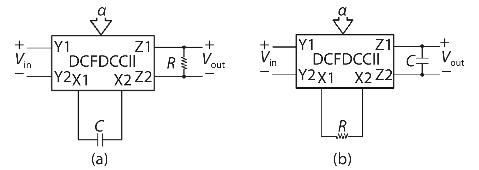
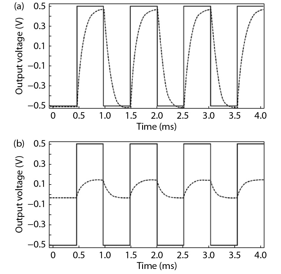
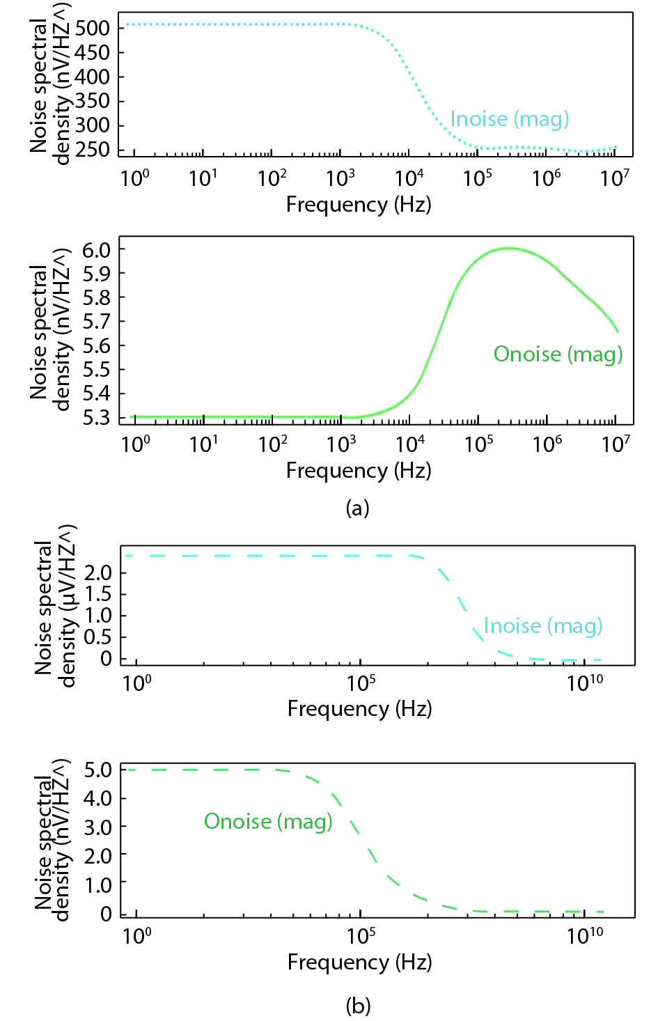
In this paper, we present a new voltage-mode biquad filter that uses a six-terminal CMOS fully differential current conveyor (FDCCII). The FDCCII with only 23 transistors in its structure and operating at ± 1.5 V, is based on a class AB fully differential buffer. The proposed filter has the facility to tune gain, ωo and Q. A circuit division circuit (CDC) is employed to digitally control the FDCCII block. This digitally controlled FDCCII is used to realize a new reconfigurable fully-differential integrator and differentiator. We performed SPICE simulations to determine the performance of all circuits using CMOS 0.25 μm technology.


J. Semicond.
2019, 40(4): 042402 doi: 10.1088/1674-4926/40/4/042402
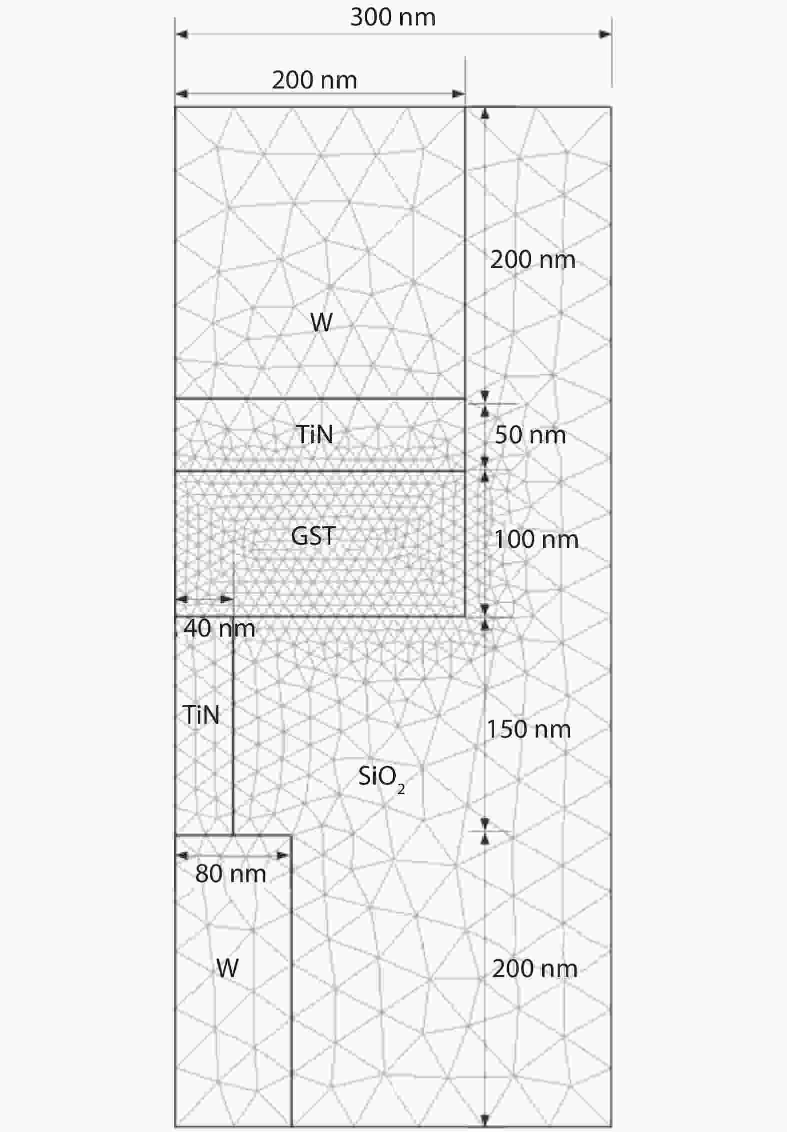
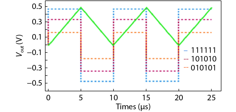
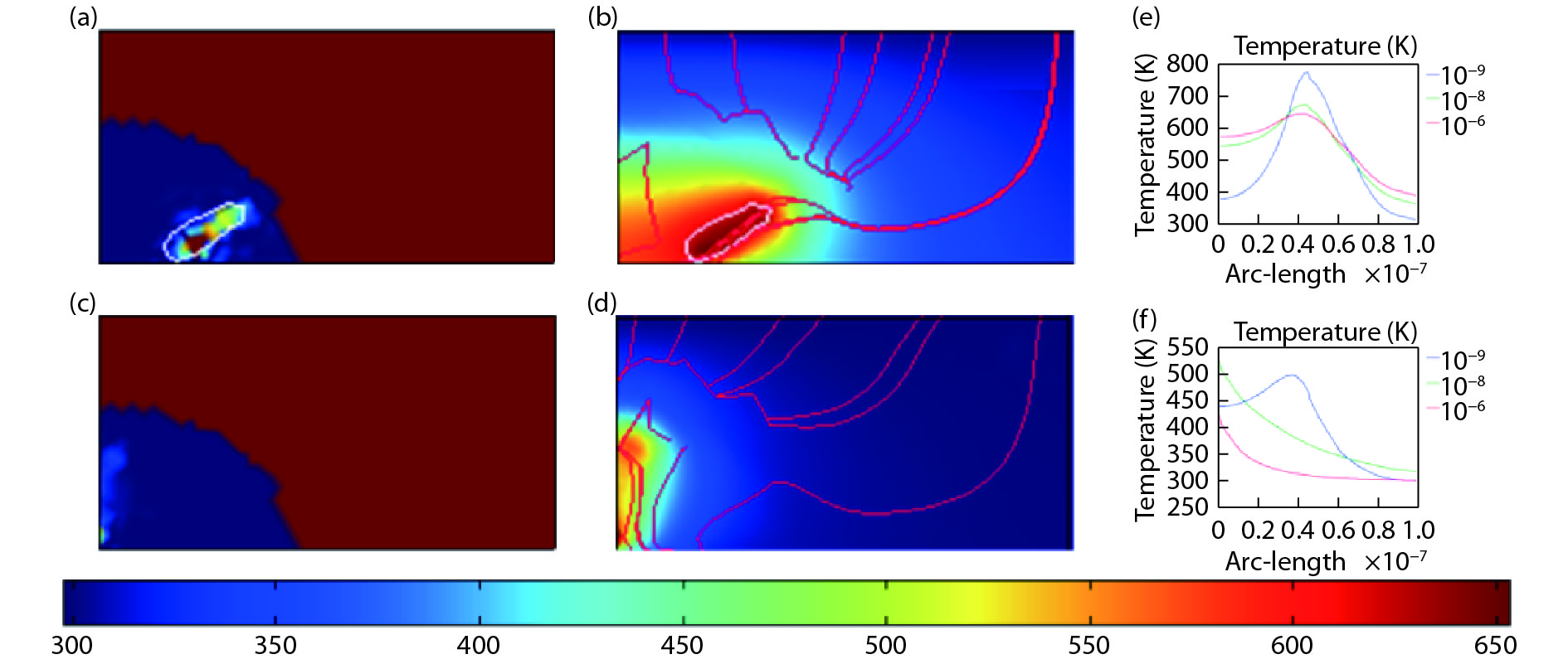
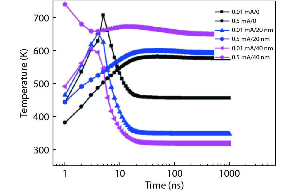
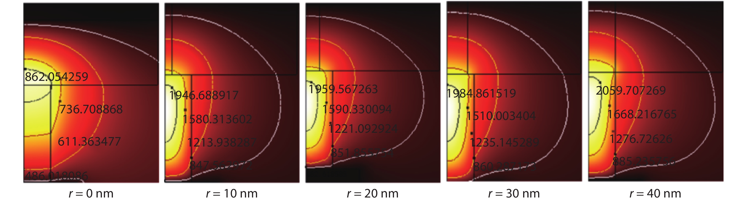
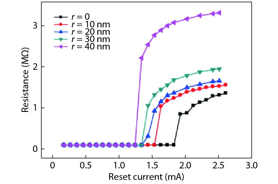
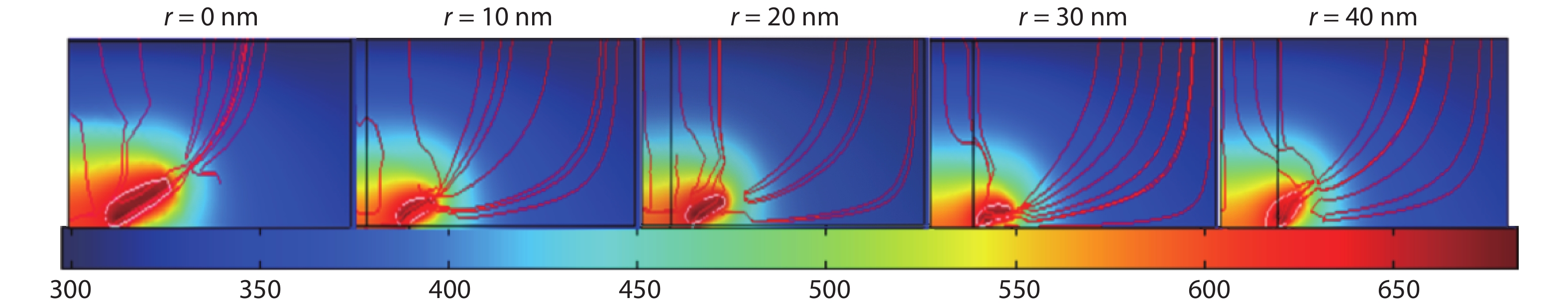
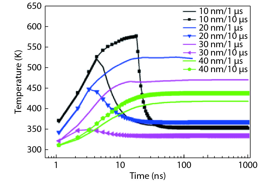
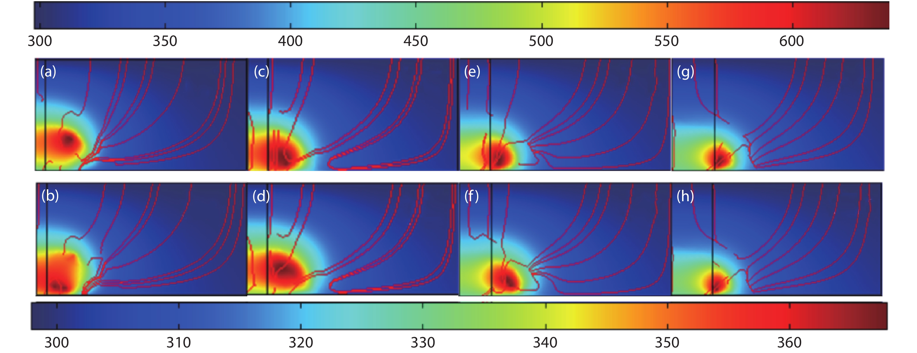
The crystallization characteristics of a ubiquitous T-shaped phase change memory (PCM) cell, under SET current pulse and very small disturb current pulse, have been investigated by finite element modelling. As analyzed in this paper, the crystallization region under SET current pulse presents first on the corner of the bottom electron contact (BEC) and then promptly forms a filament shunting down the amorphous phase to achieve the low-resistance state, whereas the tiny disturb current pulse accelerates crystallization at the axis of symmetry in the phase change material. According to the different crystallization paths, a new structure of phase change material layer is proposed to improve the data retention for PCM without impeding SET operation. This structure only requires one or two additional process steps to dope nitrogen element in the center region of phase change material layer to increase the crystallization temperature in this confined region. The electrical-thermal characteristics of PCM cells with incremental doped radius have been analyzed and the best performance is presented when the doped radius is equal to the radius of the BEC.

J. Semicond.
2019, 40(4): 042601 doi: 10.1088/1674-4926/40/4/042601

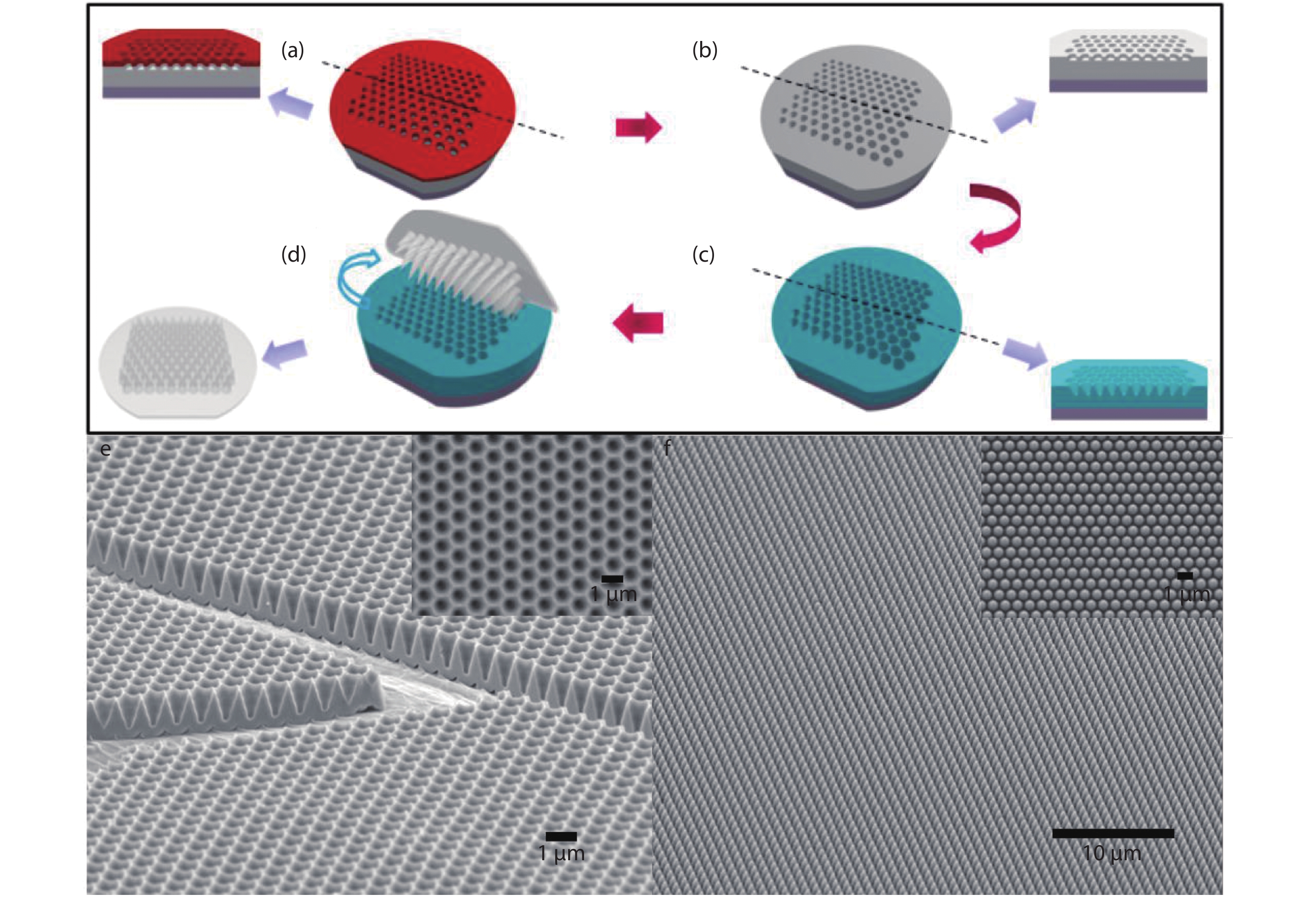
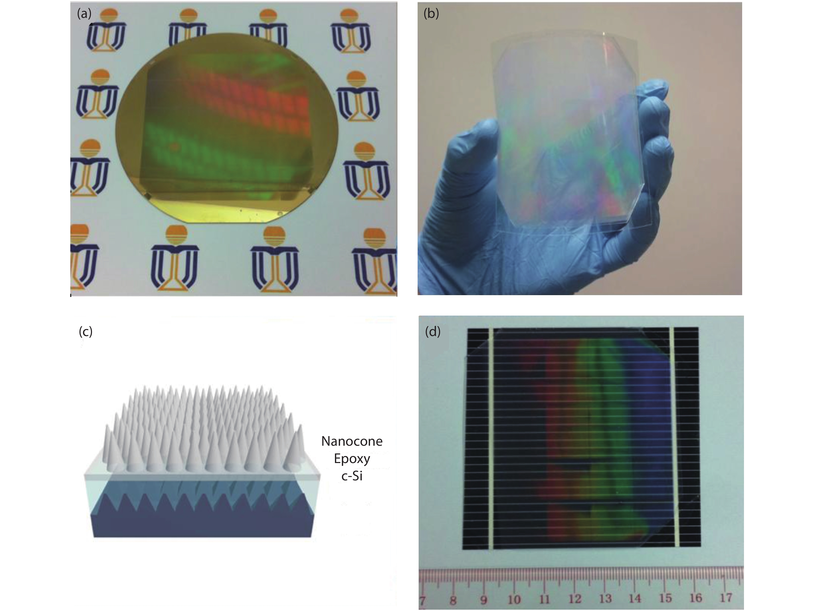
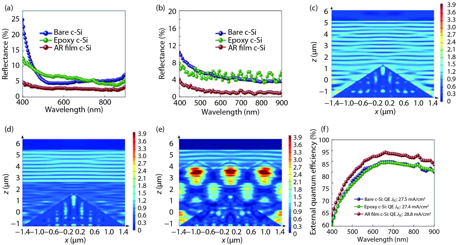
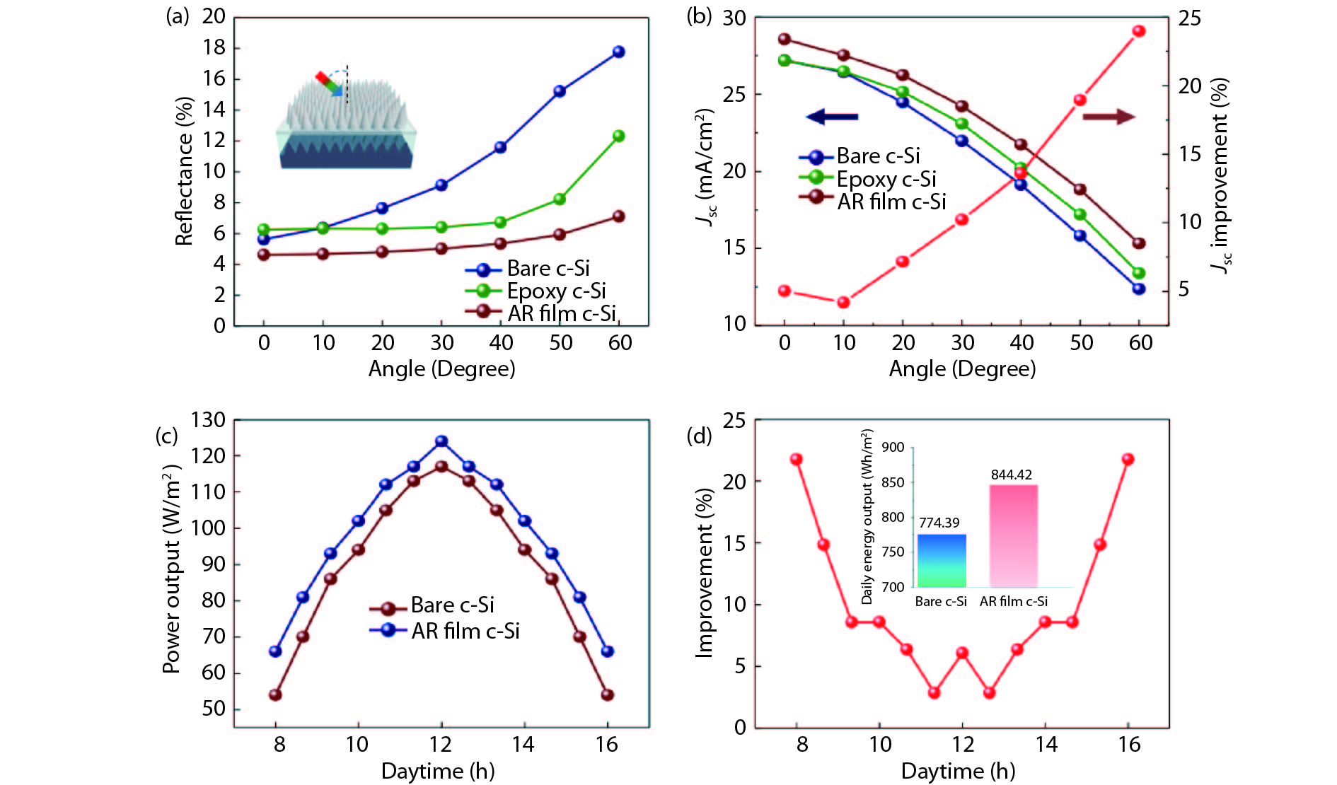
An effective and low-cost front-side anti-reflection (AR) technique has long been sought to enhance the performance of highly efficient photovoltaic devices due to its capability of maximizing the light absorption in photovoltaic devices. In order to achieve high throughput fabrication of nanostructured flexible and anti-reflection films, large-scale, nano-engineered wafer molds were fabricated in this work. Additionally, to gain in-depth understanding of the optical and electrical performance enhancement with AR films on polycrystalline Si solar cells, both theoretical and experimental studies were performed. Intriguingly, the nanocone structures demonstrated an efficient light trapping effect which reduced the surface reflection of a solar cell by 17.7% and therefore enhanced the overall electric output power of photovoltaic devices by 6% at normal light incidence. Notably, the output power improvement is even more significant at a larger light incident angle which is practically meaningful for daily operation of solar panels. The application of the developed AR films is not only limited to crystalline Si solar cells explored here, but also compatible with any types of photovoltaic technology for performance enhancement.
J. Semicond.
2019, 40(4): 042801 doi: 10.1088/1674-4926/40/4/042801
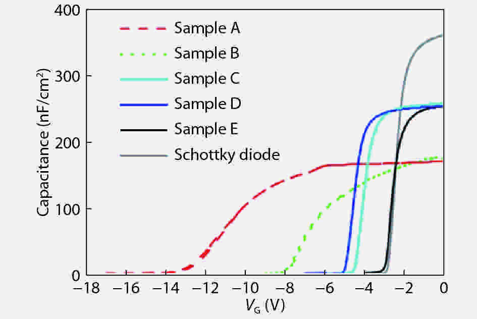
AlGaN/GaN metal–insulator–semiconductor high-electron-mobility transistors (MIS-HEMTs) on a silicon substrate were fabricated with silicon oxide as a gate dielectric by sputtering deposition and electron-beam (EB) evaporation. It was found that the oxide deposition method and conditions have great influences on the electrical properties of HEMTs. The low sputtering temperature or oxygen introduction at higher temperature results in a positive equivalent charge density at the oxide/AlGaN interface (Nequ), which induces a negative shift of threshold voltage and an increase in both sheet electron density (ns) and drain current density (ID). Contrarily, EB deposition makes a negative Nequ, resulting in reduced ns and ID. Besides, the maximum transconductance (gm-max) decreases and the off-state gate current density (IG-off) increases for oxides at lower sputtering temperature compared with that at higher temperature, possibly due to a more serious sputter-induced damage and much larger Nequ at lower sputtering temperature. At high sputtering temperature, IG-off decreases by two orders of magnitude compared to that without oxygen, which indicates that oxygen introduction and partial pressure depression of argon decreases the sputter-induced damage significantly. IG-off for EB-evaporated samples is lower by orders of magnitude than that of sputtered ones, possibly attributed to the lower damage of EB evaporation to the barrier layer surface.


J. Semicond.
2019, 40(4): 042901 doi: 10.1088/1674-4926/40/4/042901
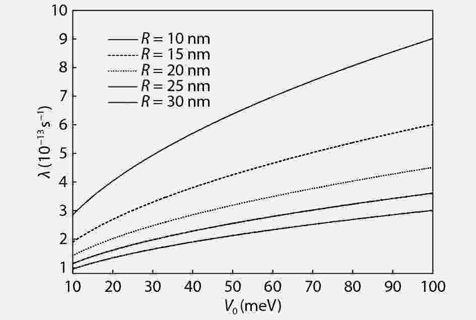
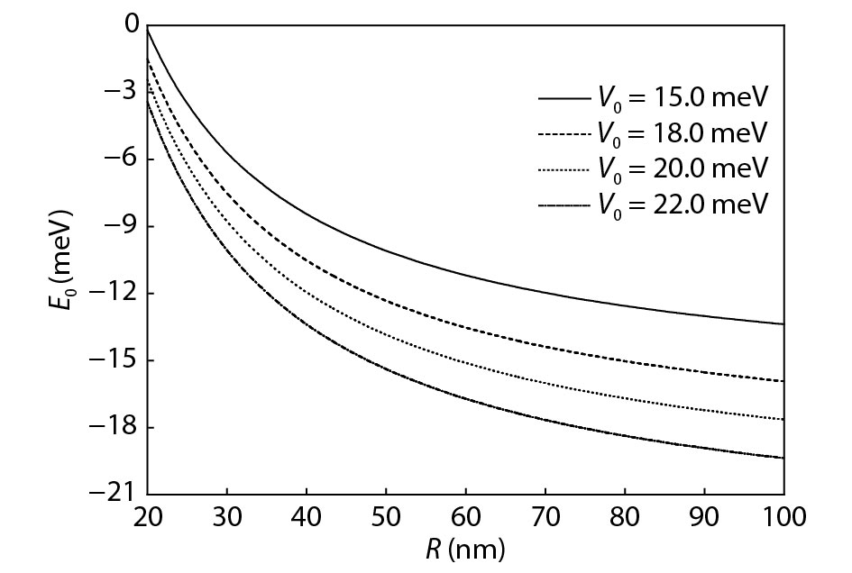
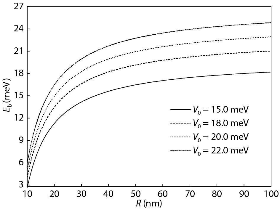
The vibrational frequency (VF), the ground state (GS) energy and the GS binding energy of the weak electron-phonon coupling polaron in a quantum well (QW) with asymmetrical Gaussian confinement potential are calculated. First we introduce the linear combination operator to express the momentum and coordinates in the Hamilton and then operate the system Hamilton using unitary transformation. The results indicate the relations of the quantities (the VF, the absolute value of GS energy and the GS binding energy) and the parameters (the QW barrier height and the range of Gaussian confinement potential in the growth direction of the QW).