Issue Browser
Volume 40, Issue 7,
Jul 2019
J. Semicond.
2019, 40(7): 070301 doi: 10.1088/1674-4926/40/7/070301
Semiconductor provides a physics-rich environment to host various quantum light sources applicable for quantum information processing. These light sources are capable of deterministic generation of non-classical photon streams that demonstrate antibunching photon statistics, strong indistinguishability, and high-fidelity entanglement. Some of them have even successfully transitioned from proof-of-concept to engineering efforts with steadily improving performance[


J. Semicond.
2019, 40(7): 071901 doi: 10.1088/1674-4926/40/7/071901
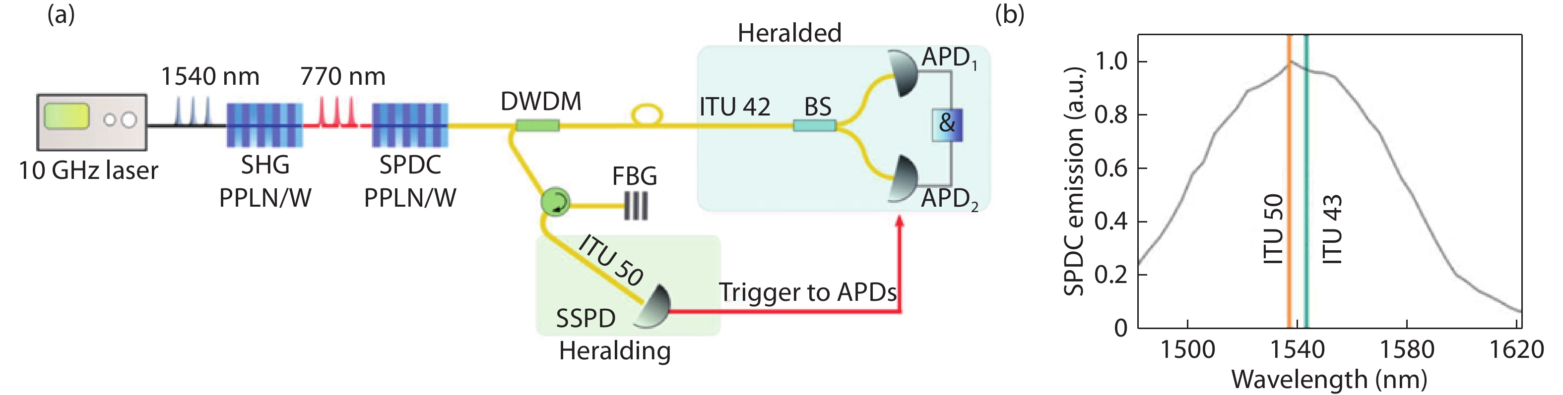
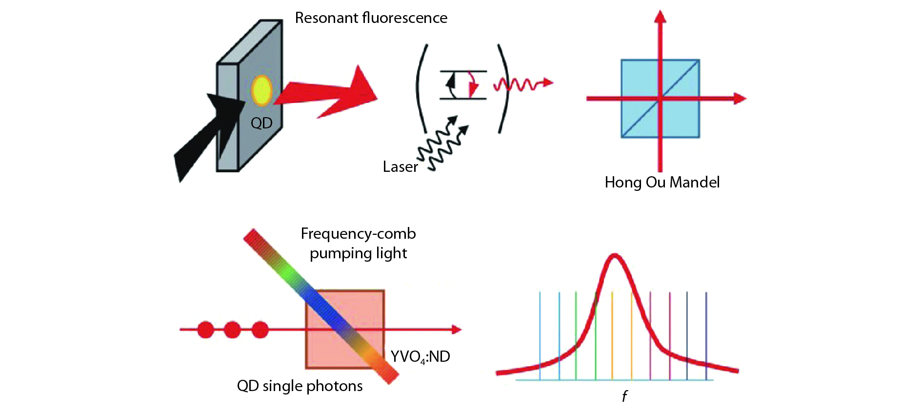
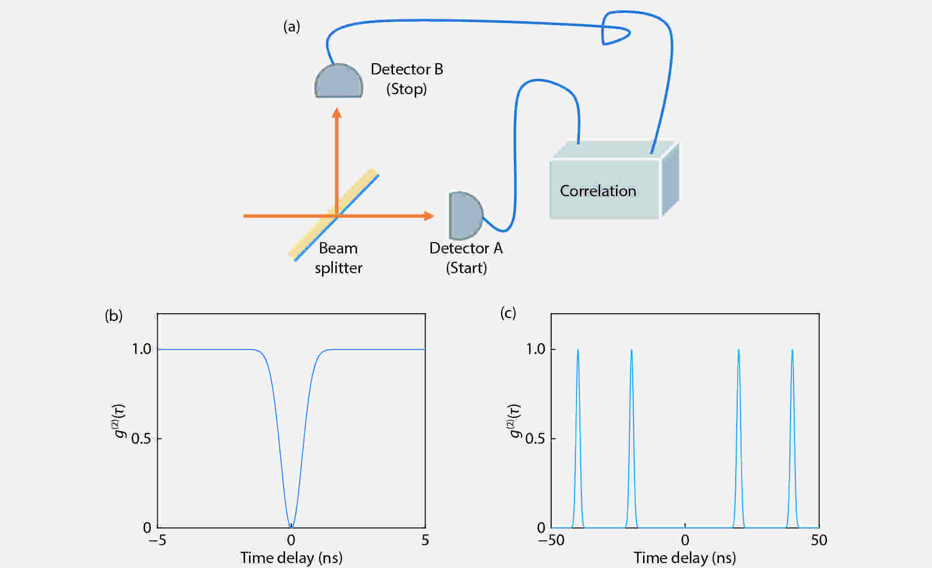
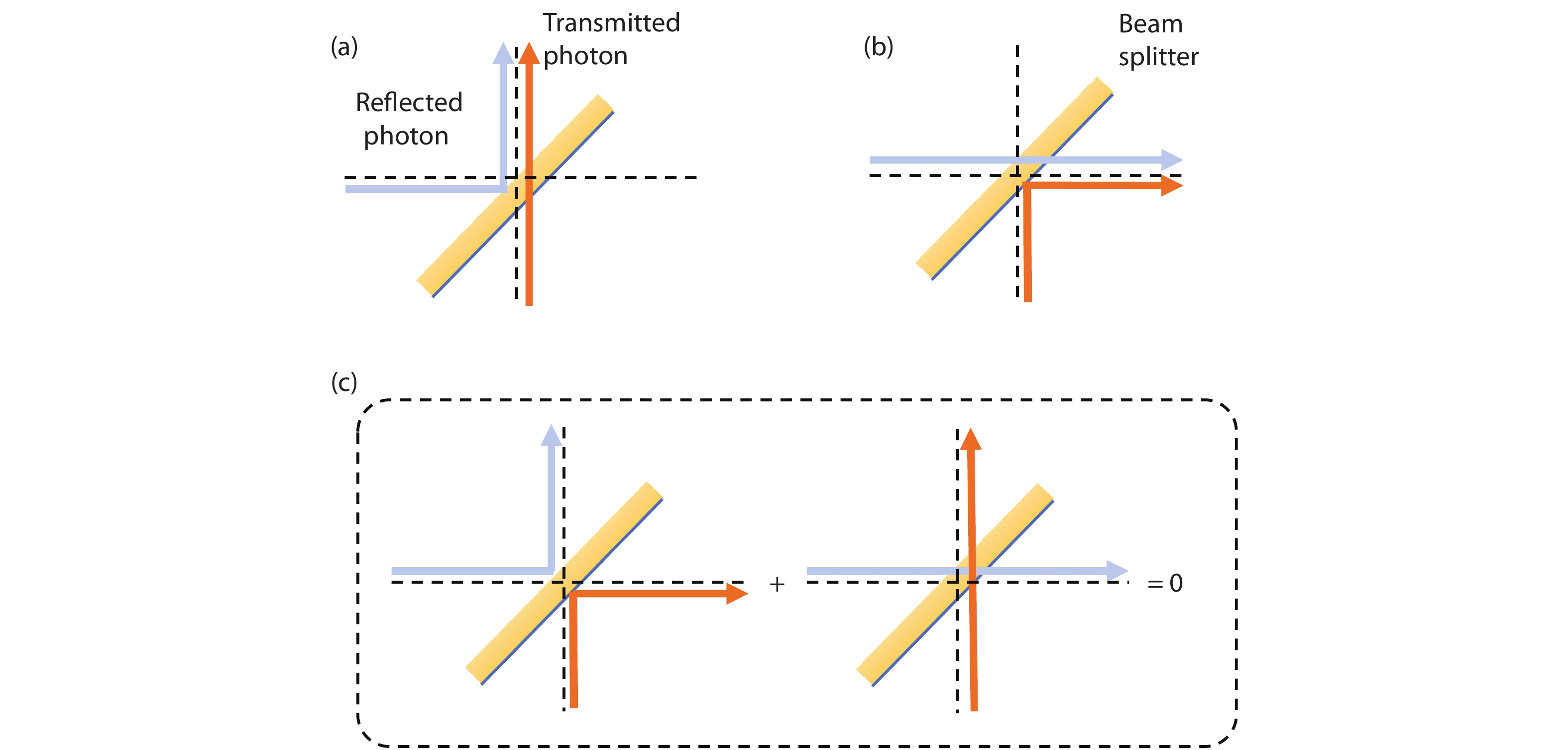
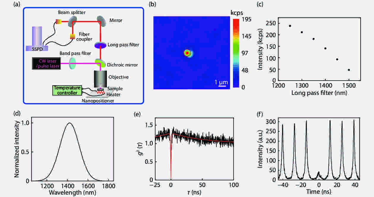
Single photon sources are key components for quantum technologies such as quantum communication, computing and metrology. A key challenge towards the realization of global quantum networks are transmission losses in optical fibers. Therefore, single photon sources are required to emit at the low-loss telecom wavelength bands. However, an ideal telecom wavelength single photon source has yet to be discovered. Here, we review the recent progress in realizing such sources. We start with single photon emission based on atomic ensembles and spontaneous parametric down conversion, and then focus on solid-state emitters including semiconductor quantum dots, defects in silicon carbide and carbon nanotubes. In conclusion, some state-of-the-art applications are highlighted.


J. Semicond.
2019, 40(7): 071902 doi: 10.1088/1674-4926/40/7/071902

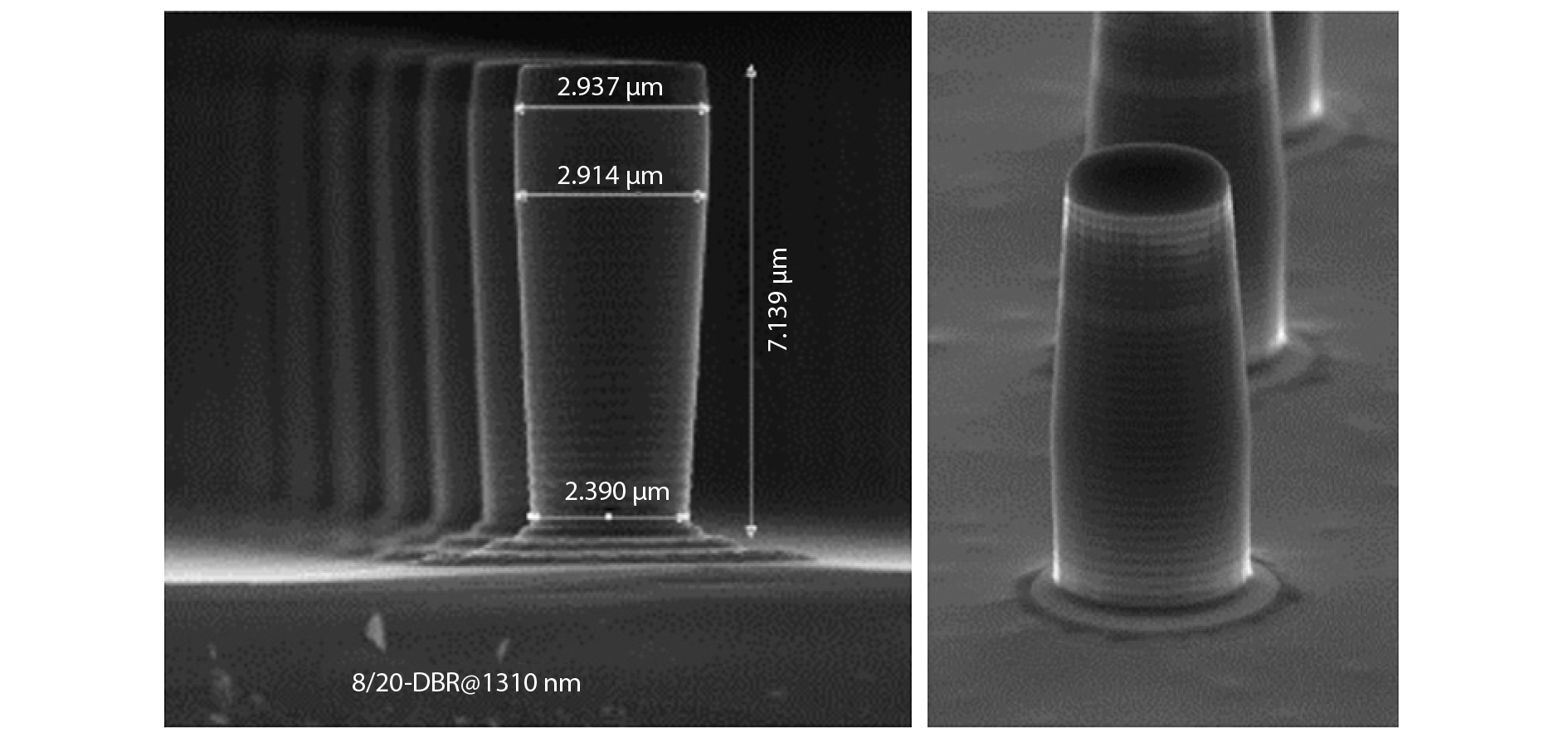
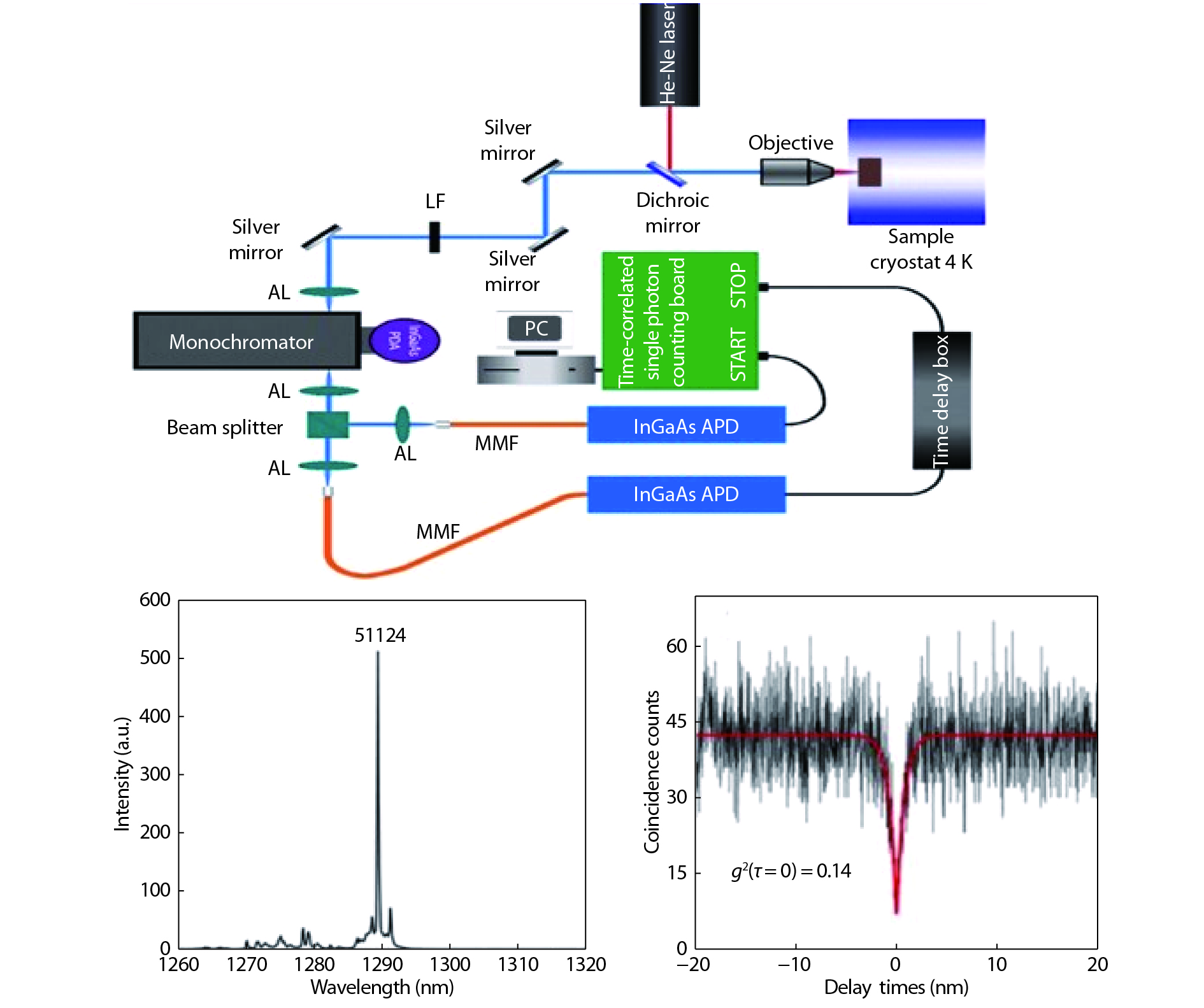
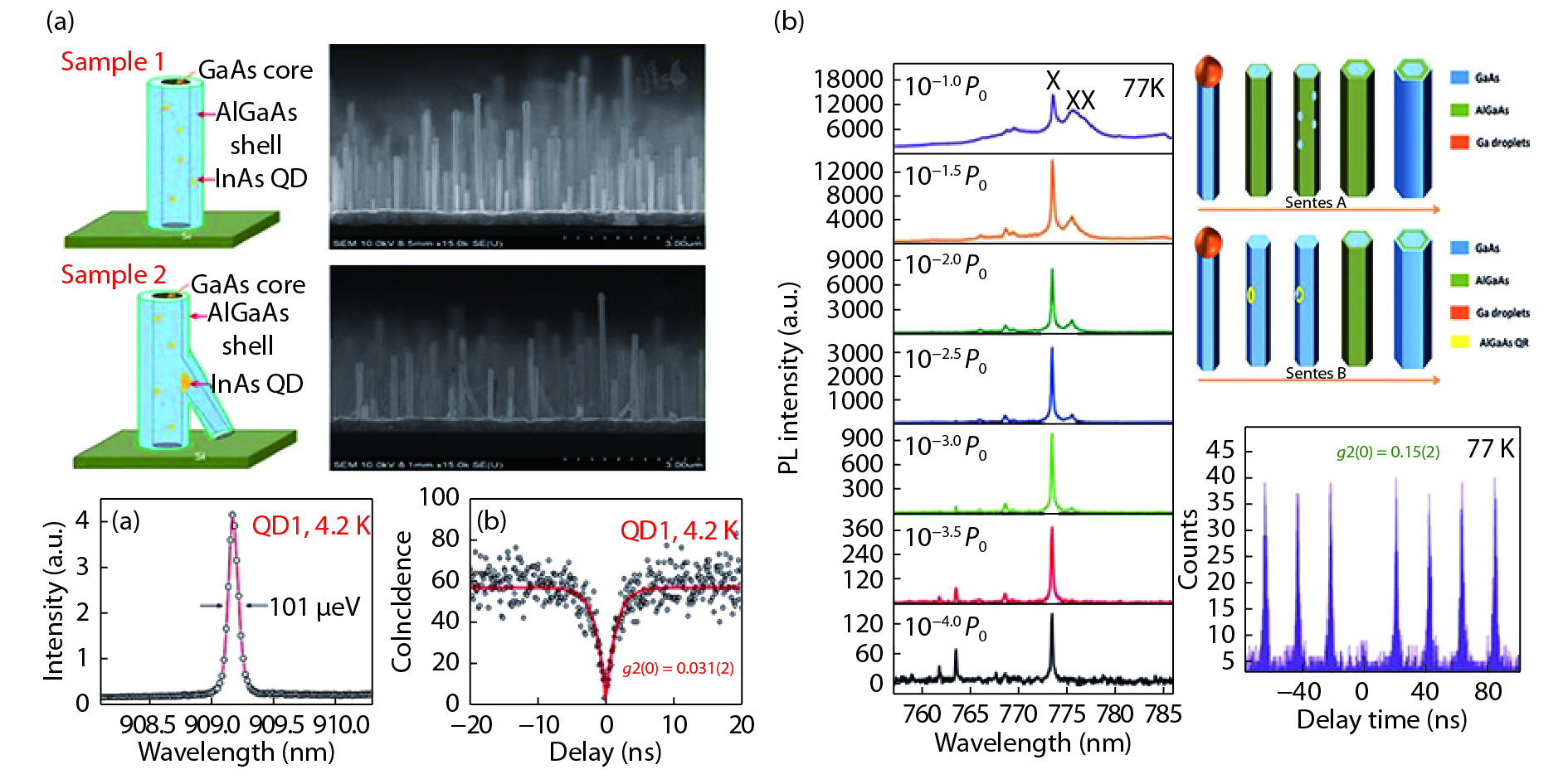
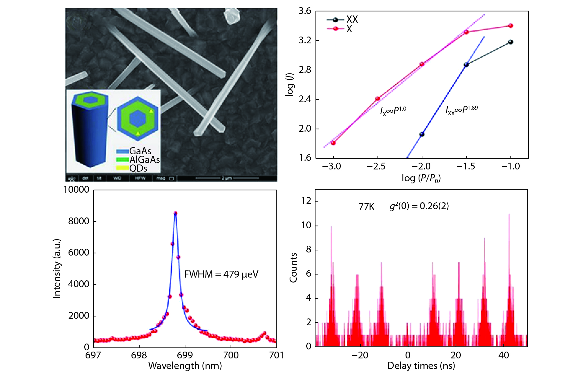
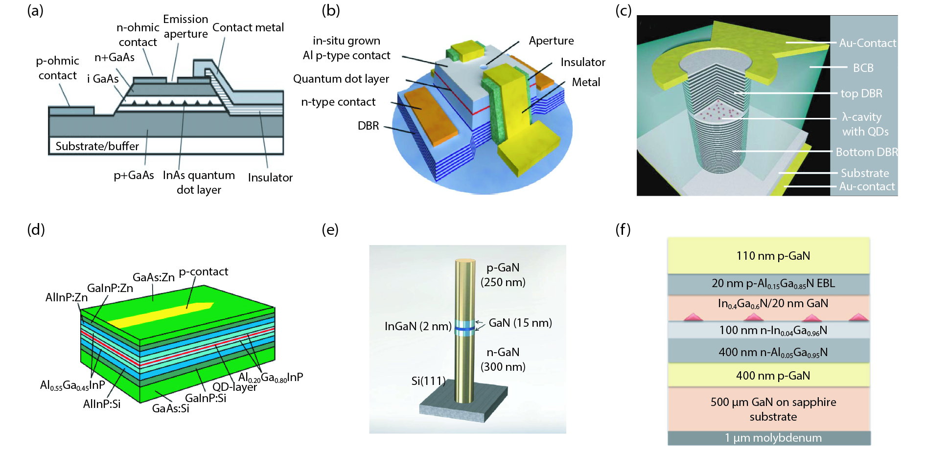
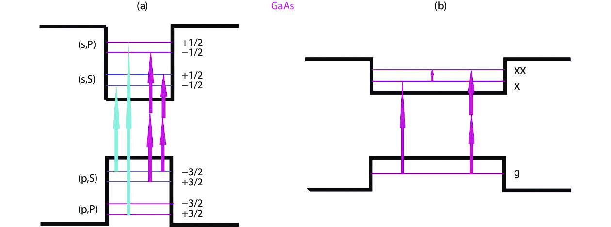
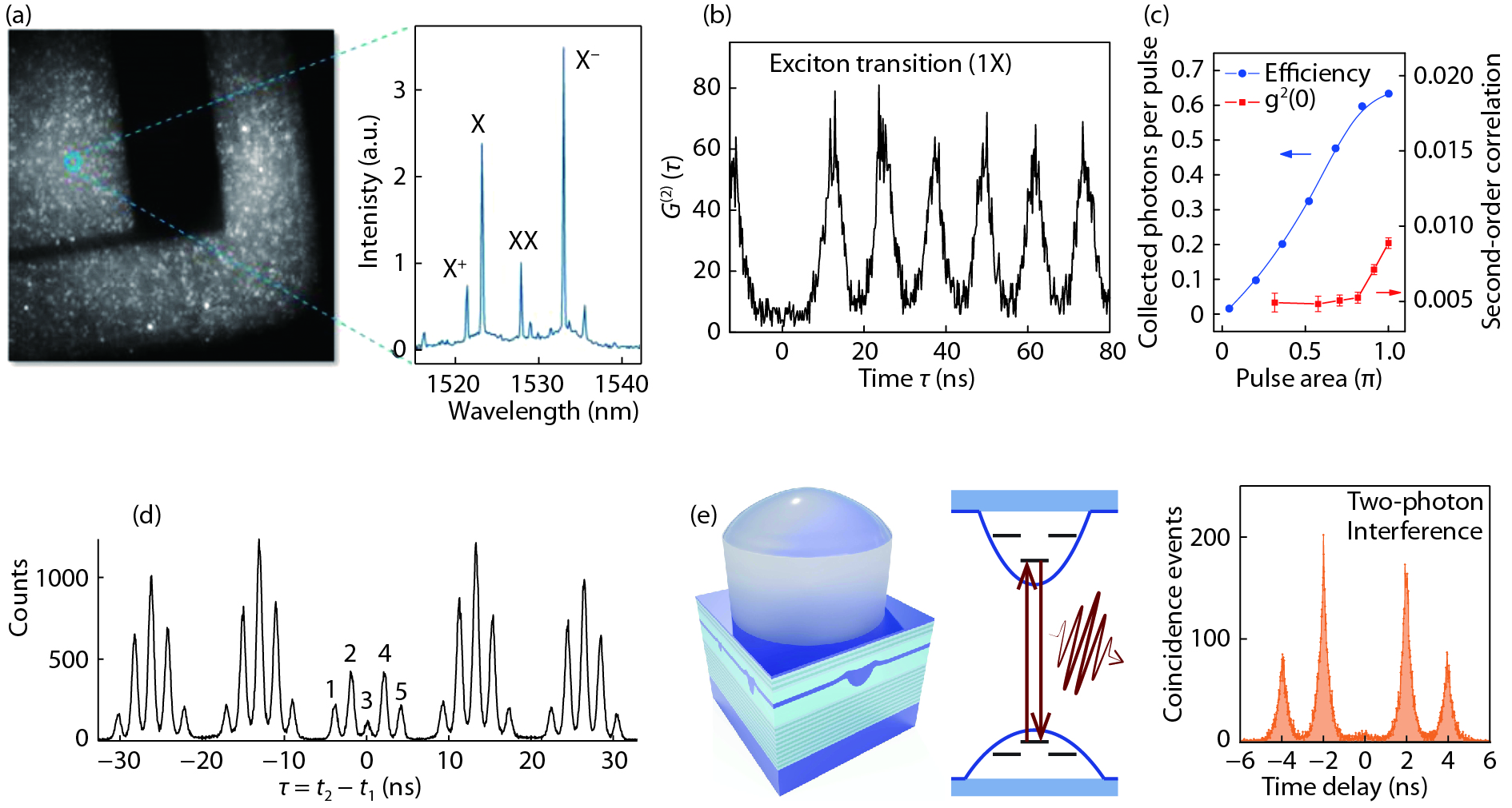
A brief introduction of semiconductor self-assembled quantum dots (QDs) applied in single-photon sources is given. Single QDs in confined quantum optical microcavity systems are reviewed along with their optical properties and coupling characteristics. Subsequently, the recent progresses in In(Ga)As QDs systems are summarized including the preparation of quantum light sources, multiple methods for embedding single QDs into different microcavities and the scalability of single-photon emitting wavelength. Particularly, several In(Ga)As QD single-photon devices are surveyed including In(Ga)As QDs coupling with nanowires, InAs QDs coupling with distributed Bragg reflection microcavity and the In(Ga)As QDs coupling with micropillar microcavities. Furthermore, applications in the field of single QDs technology are illustrated, such as the entangled photon emission by spontaneous parametric down conversion, the single-photon quantum storage, the chip preparation of single-photon sources as well as the single-photon resonance-fluorescence measurements.
J. Semicond.
2019, 40(7): 071903 doi: 10.1088/1674-4926/40/7/071903
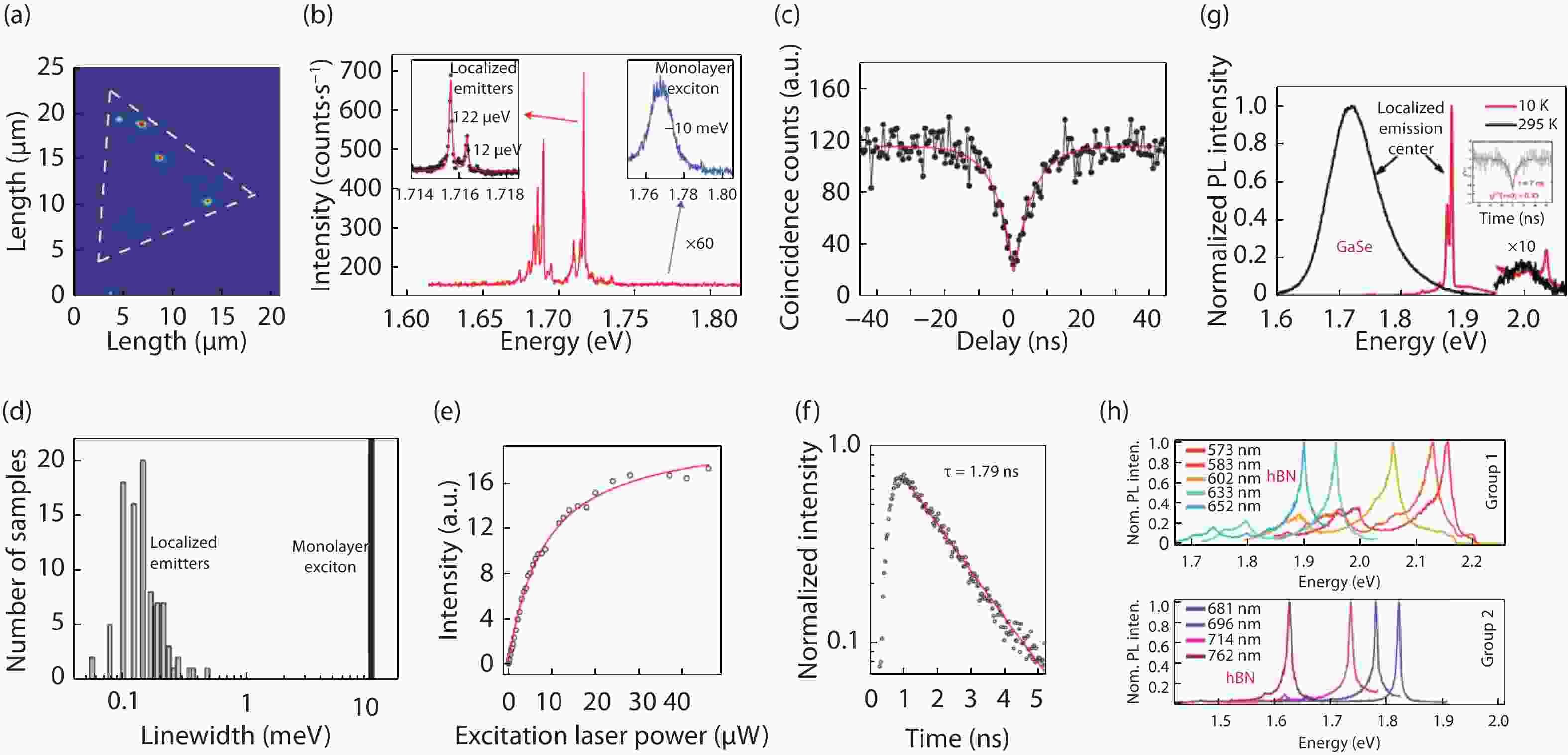
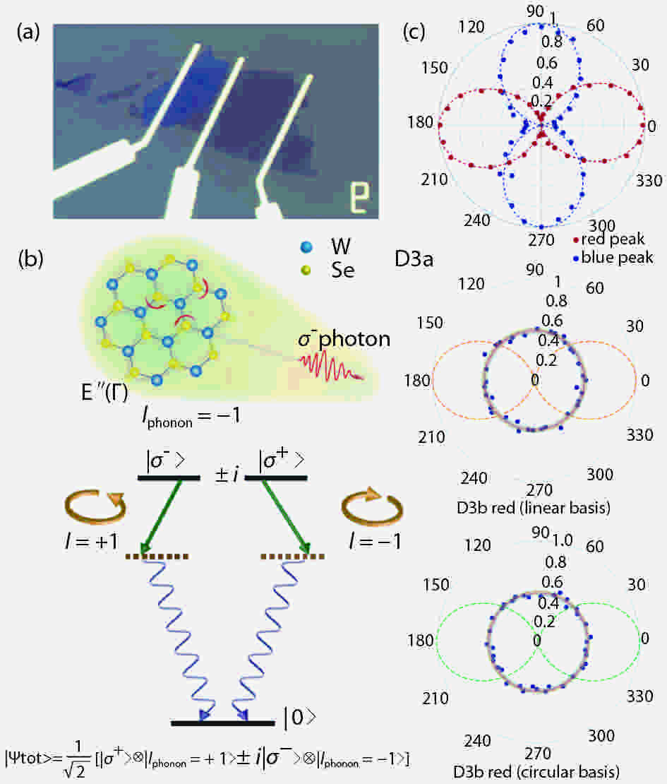
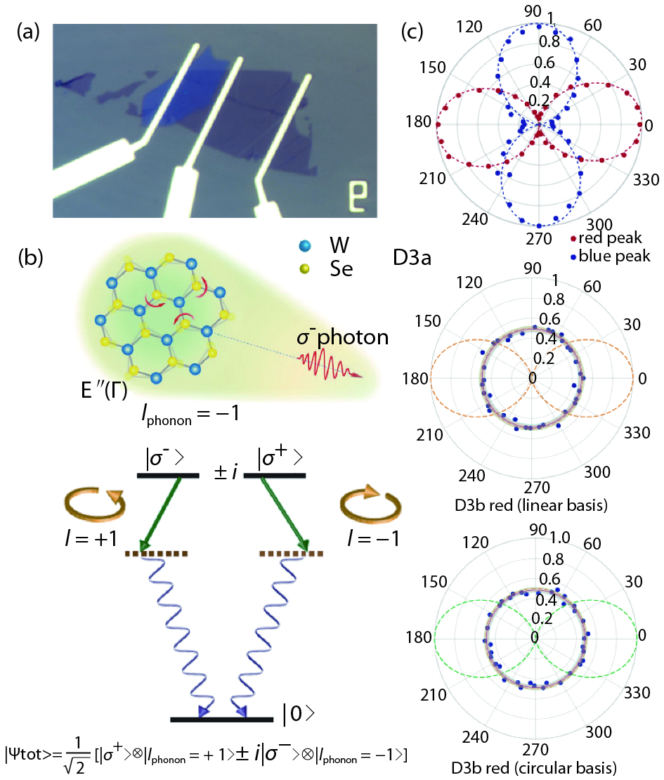
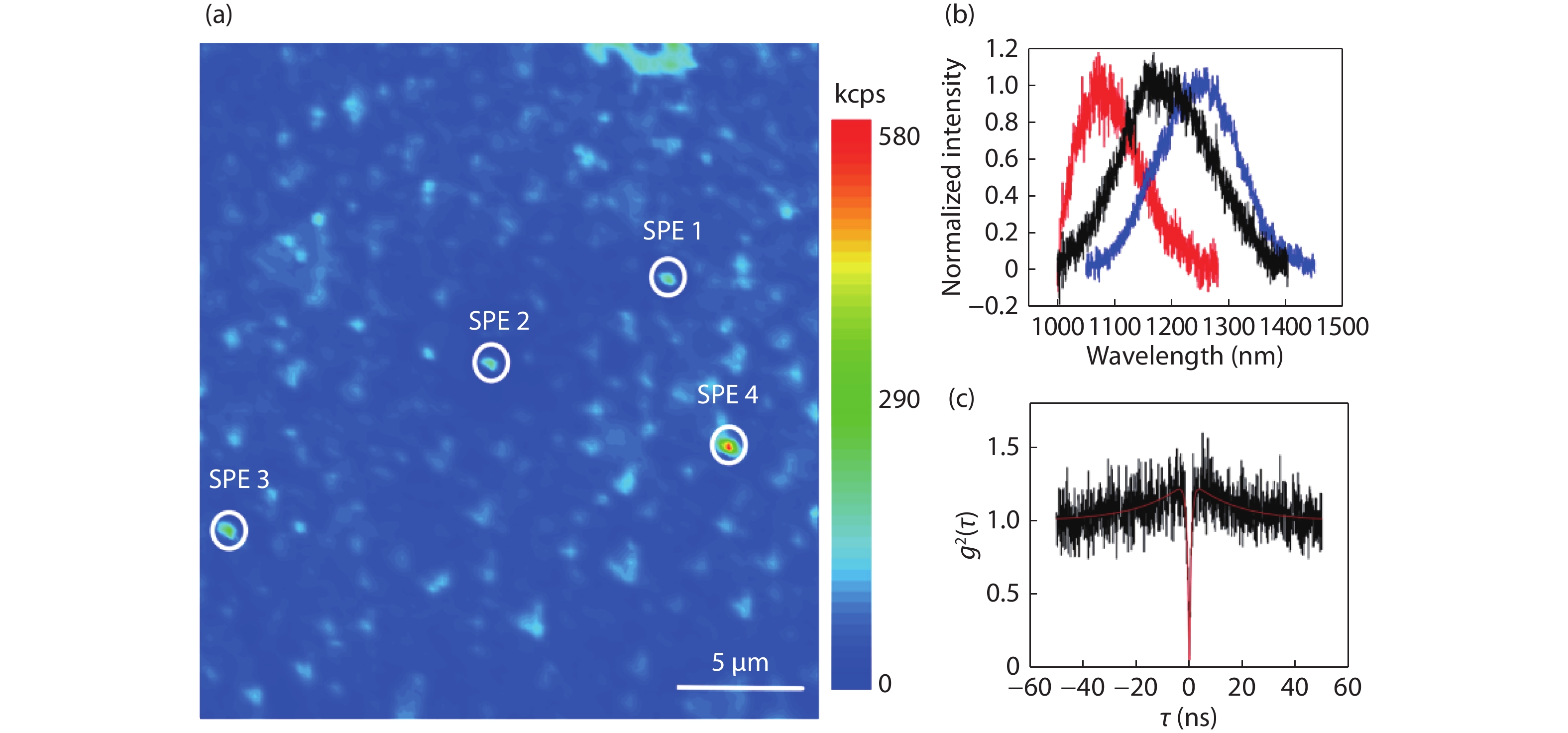
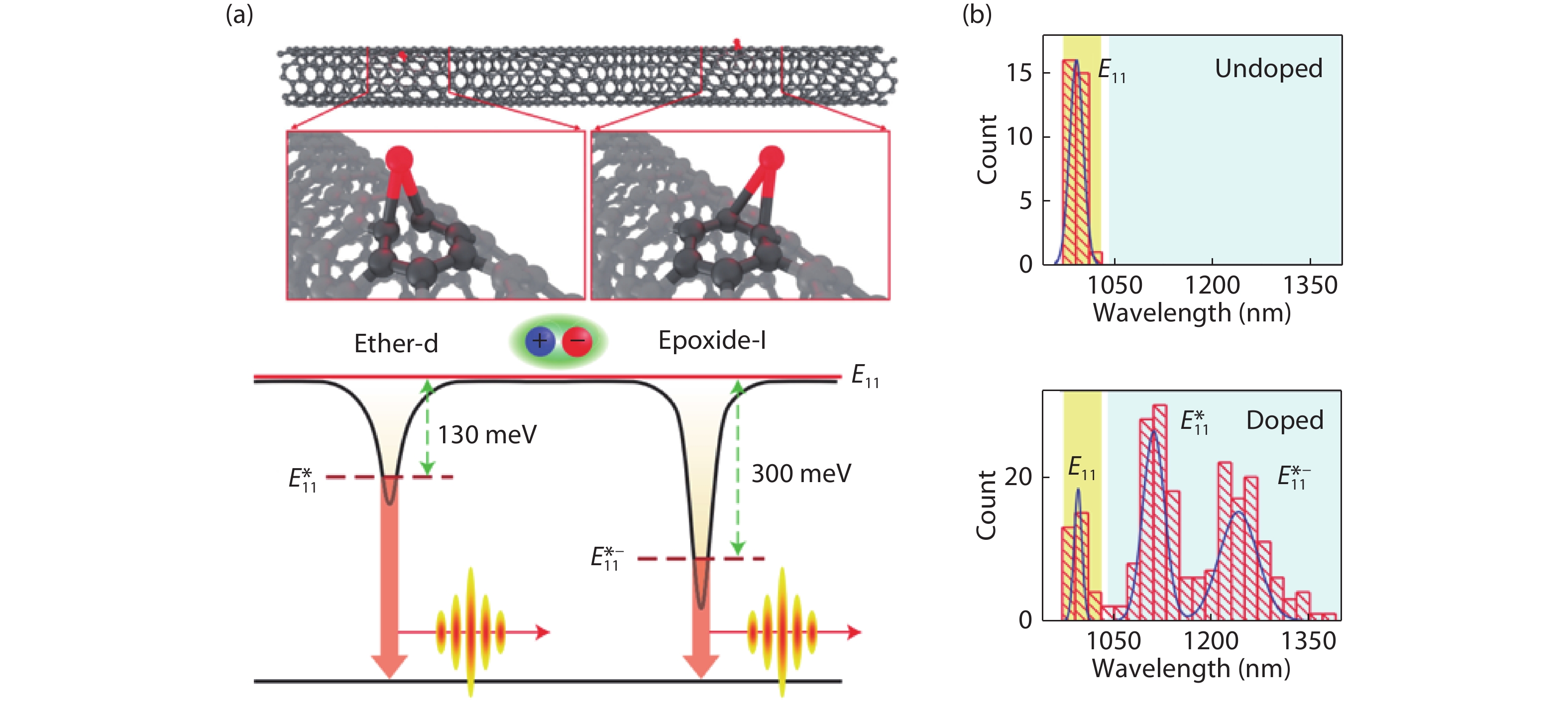
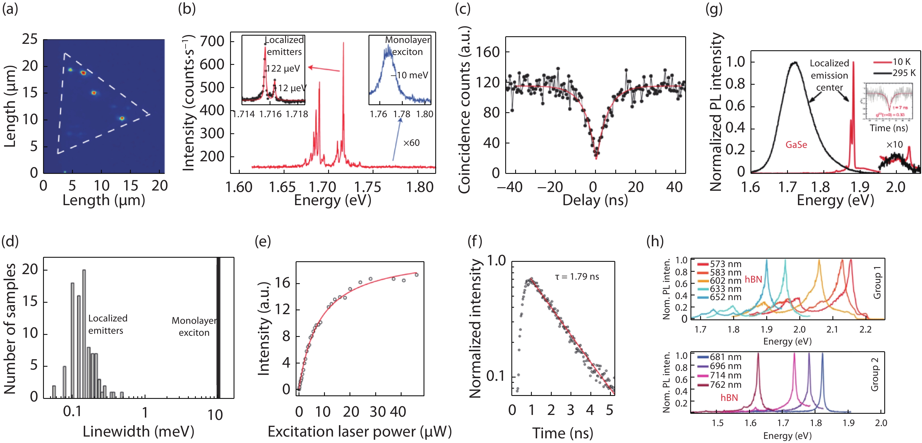
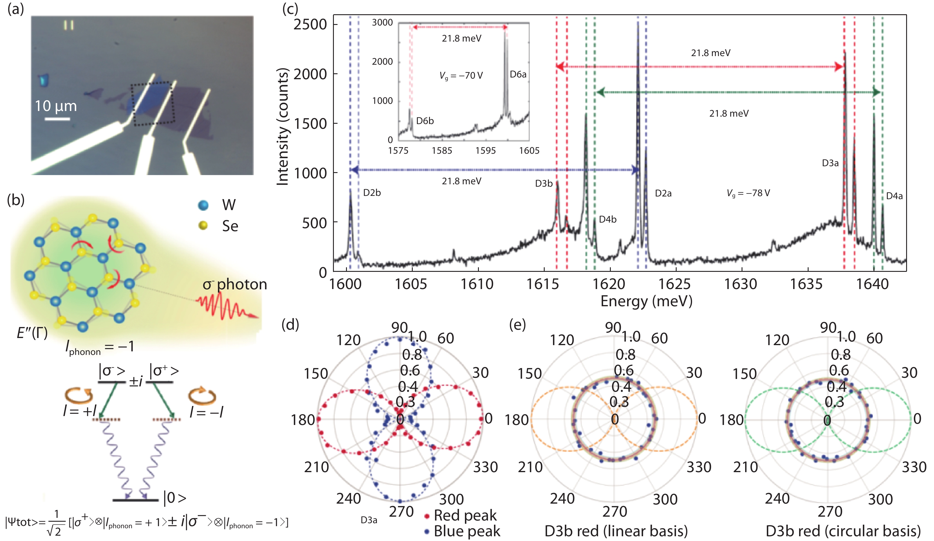
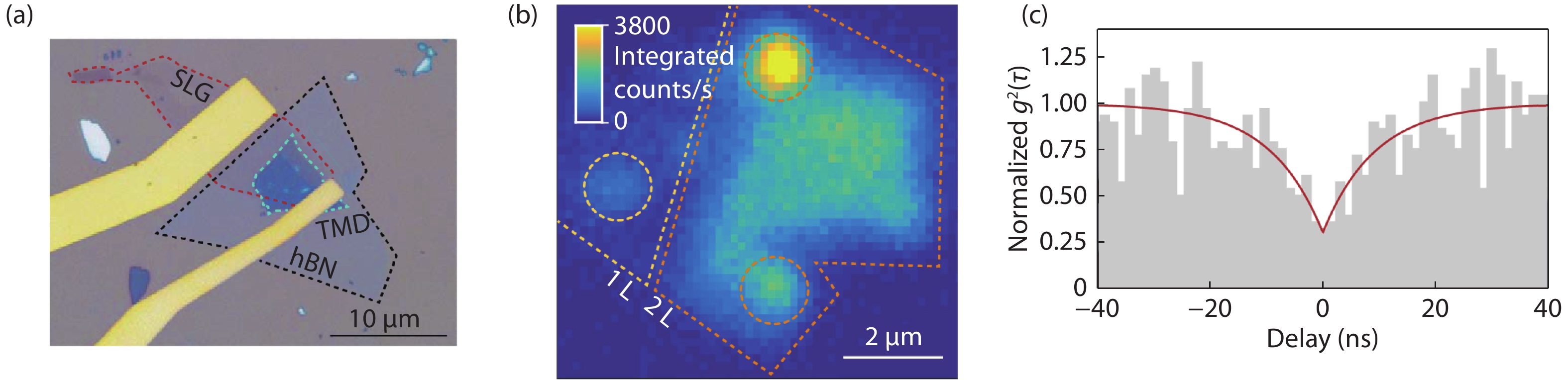
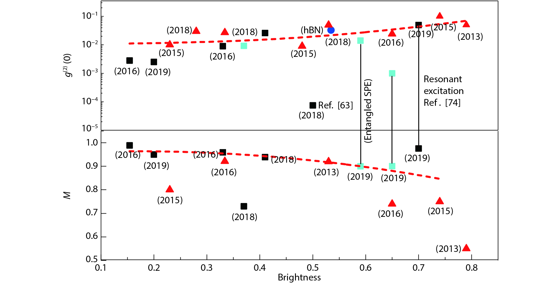
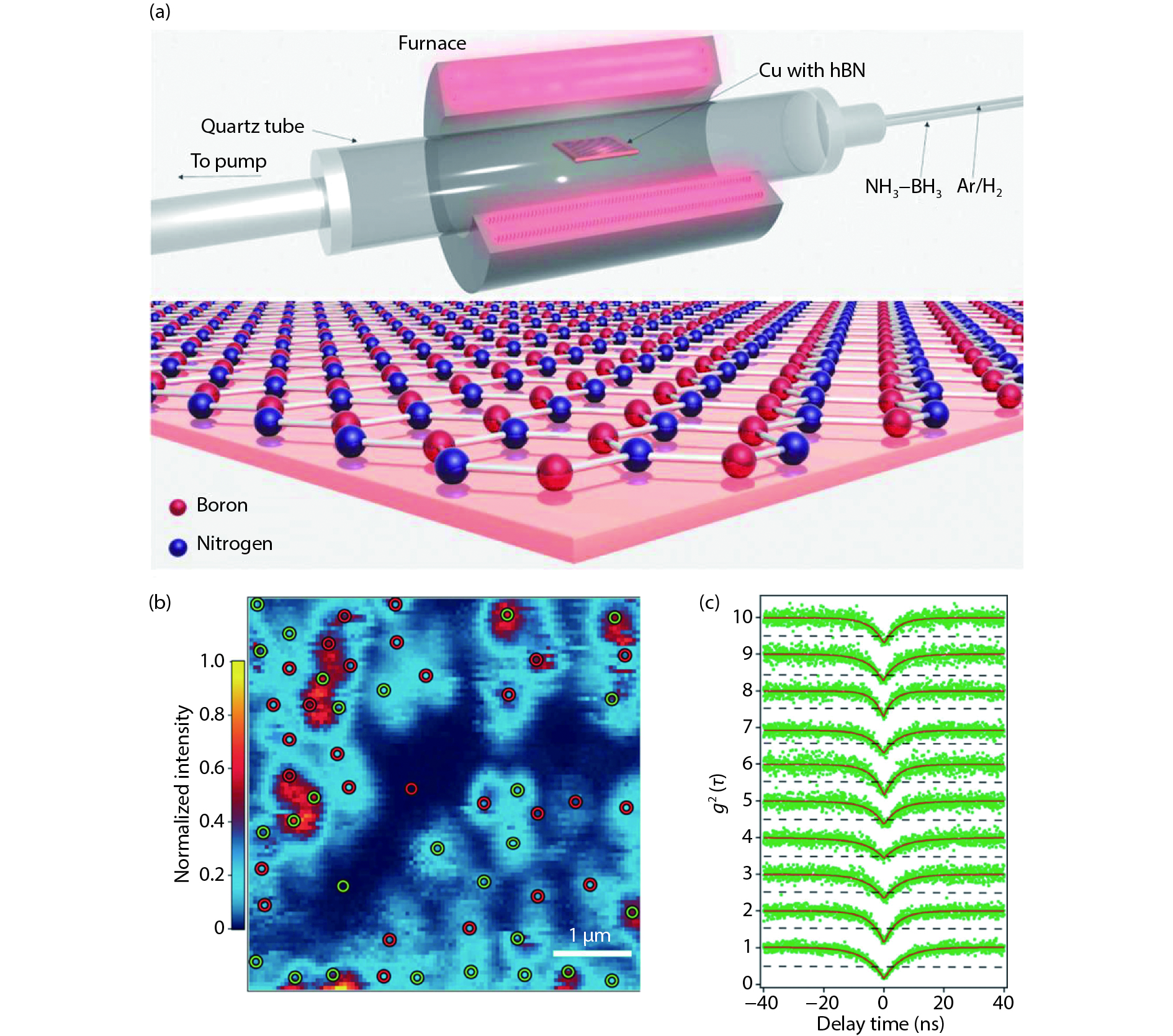
The solid state single photon source is fundamental key device for application of quantum communication, quantum computing, quantum information and quantum precious metrology. After years of searching, researchers have found the single photon emitters in zero-dimensional quantum dots (QDs), one-dimensional nanowires, three-dimensional wide bandgap materials, as well as two-dimensional (2D) materials developed recently. Here we will give a brief review on the single photon emitters in 2D van der Waals materials. We will firstly introduce the quantum emitters from various 2D materials and their characteristics. Then we will introduce the electrically driven quantum light in the transition metal dichalcogenides (TMDs)-based light emitting diode (LED). In addition, we will introduce how to tailor the quantum emitters by nanopillars and strain engineering, the entanglement between chiral phonons (CPs) and single photon in monolayer TMDs. Finally, we will give a perspective on the opportunities and challenges of 2D materials-based quantum light sources.


J. Semicond.
2019, 40(7): 071904 doi: 10.1088/1674-4926/40/7/071904
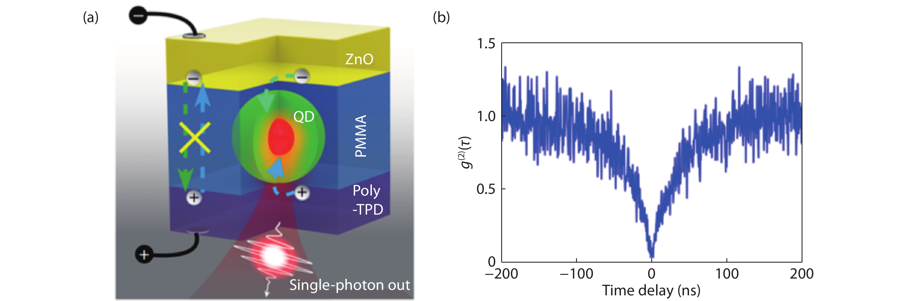
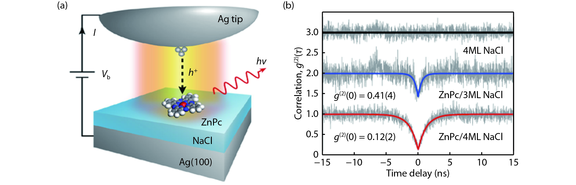
Single-photon sources are building blocks for photonic quantum information processes. Of the many single-photon generation schemes, electrically driven single-photon sources have the advantages of realizing monolithic integration of quantum light sources and detectors without optical filtering, thus greatly simplify the integrated quantum photonic circuits. Here, we review recent advances on electrically driven single-photon sources based on solid-state quantum emitters, such as semiconductor epitaxial quantum dots, colloidal quantum dots, carbon nanotubes, molecules, and defect states in diamond, SiC and layered semiconductors. In particular, the merits and drawbacks of each system are discussed. Finally, the article is concluded by discussing the challenges that remain for electrically driven single-photon sources.


J. Semicond.
2019, 40(7): 071905 doi: 10.1088/1674-4926/40/7/071905
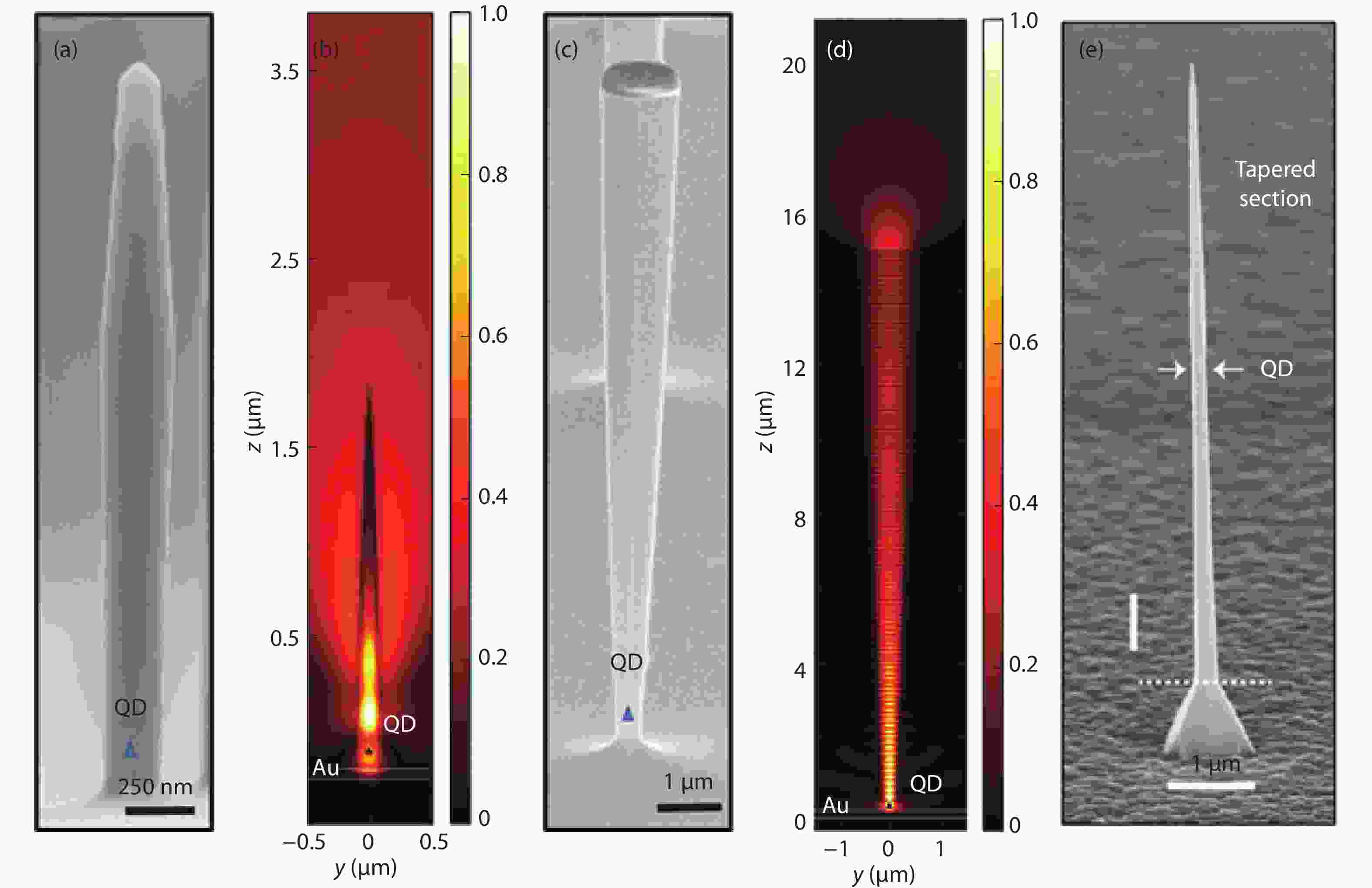
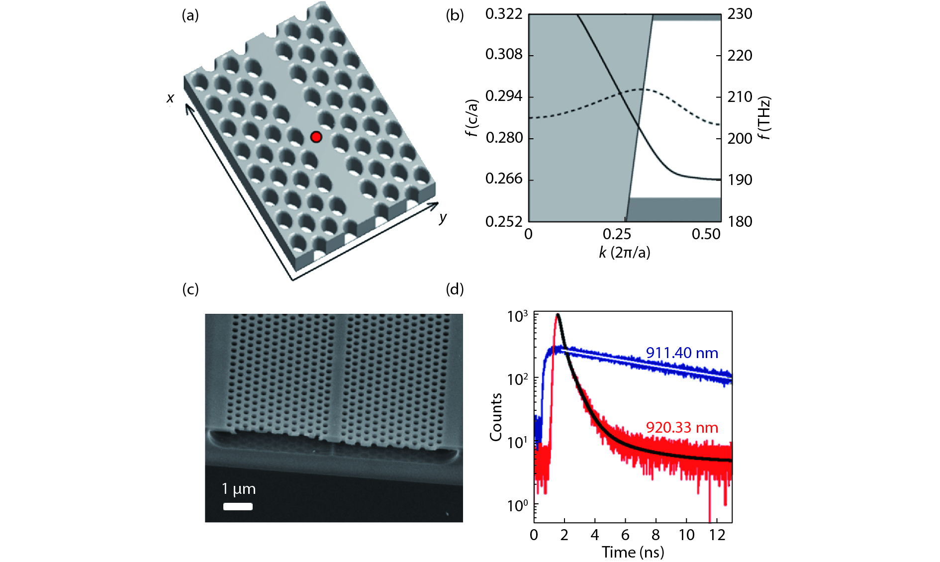
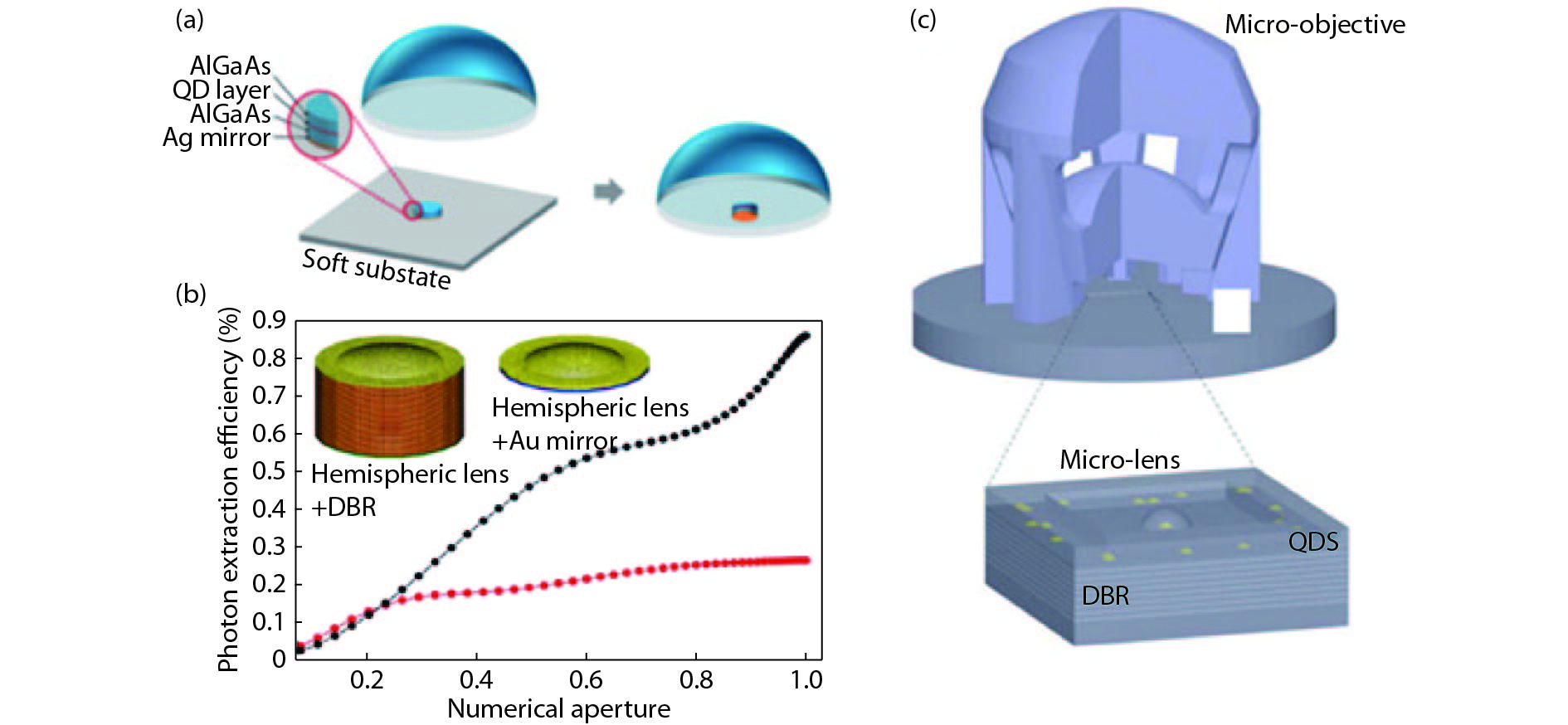
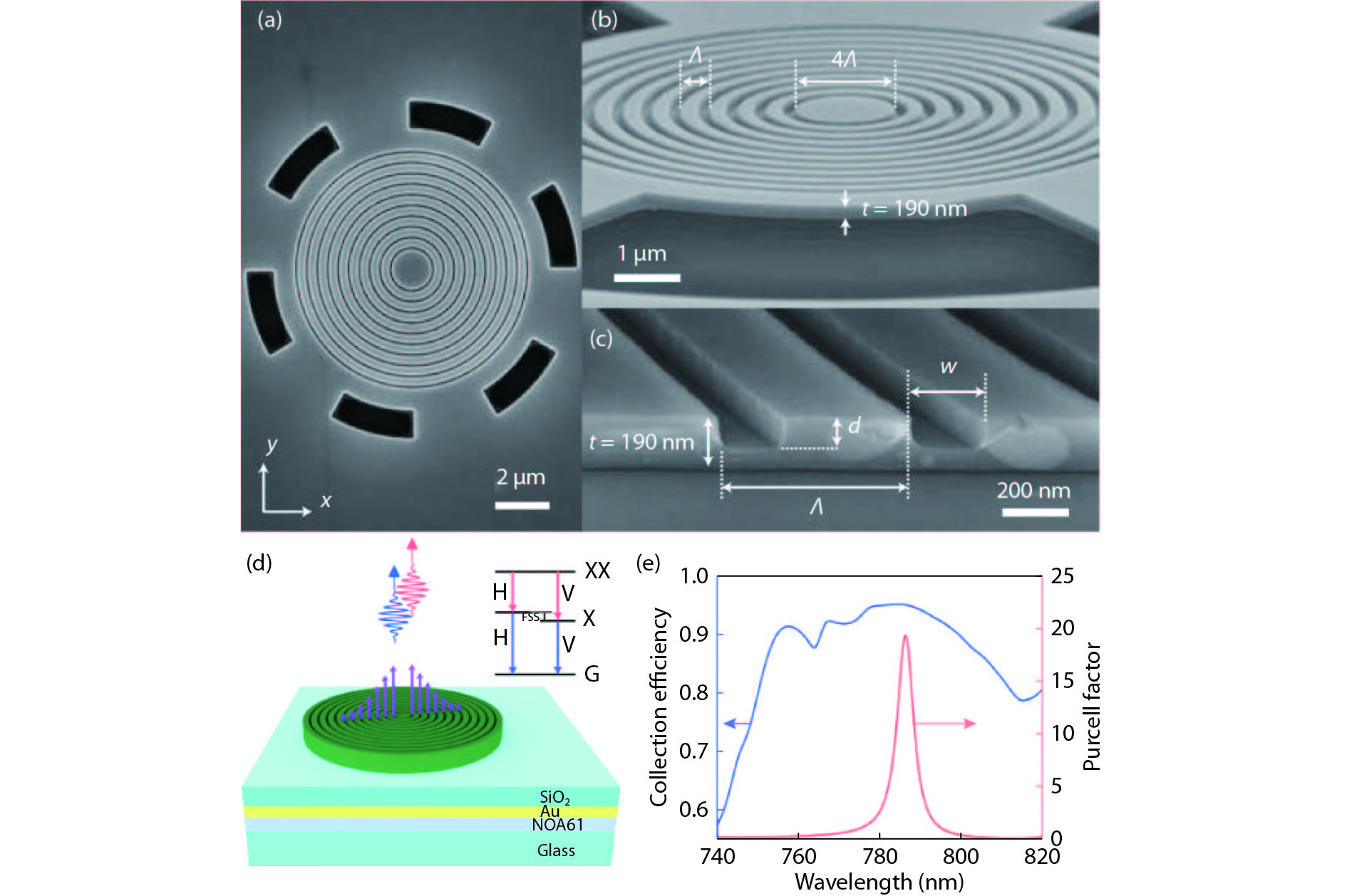
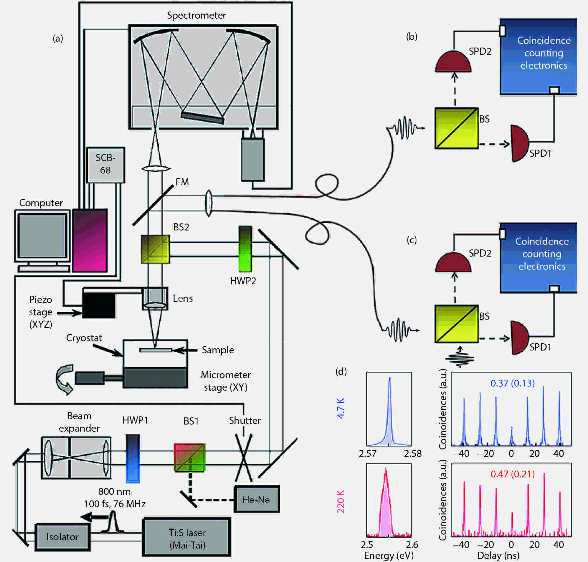
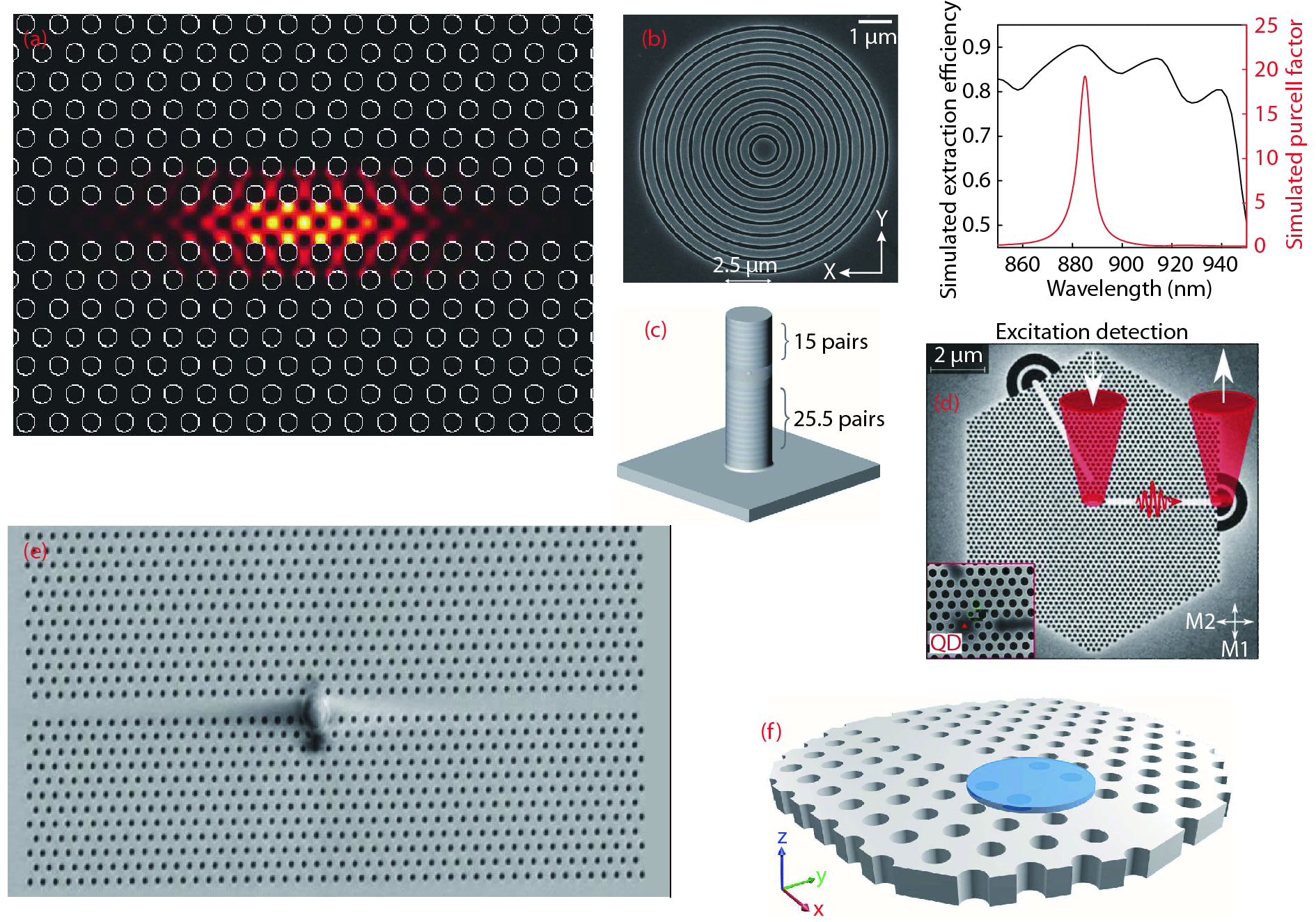
Quantum light sources serve as one of the key elements in quantum photonic technologies. Such sources made from semiconductor material, e.g., quantum dots (QDs), are particularly appealing because of their great potential of scalability enabled by the modern planar nanofabrication technologies. So far, non-classic light sources based on semiconductor QDs are currently outperforming their counterparts using nonlinear optical process, for instance, parametric down conversion and four-wave mixing. To fully exploring the potential of semiconductor QDs, it is highly desirable to integrate QDs with a variety of photonic nanostructures for better device performance due to the improved light-matter interaction. Among different designs, the photonic nanostructures exhibiting broad operation spectral range is particularly interesting to overcome the QD spectral inhomogeneity and exciton fine structure splitting for the generations of single-photon and entangled photon pair respectively. In this review, we focus on recent progress on high-performance semiconductor quantum light sources that is achieved by integrating single QDs with a variety of broadband photonic nanostructures i.e. waveguide, lens and low-Q cavity.

J. Semicond.
2019, 40(7): 071906 doi: 10.1088/1674-4926/40/7/071906
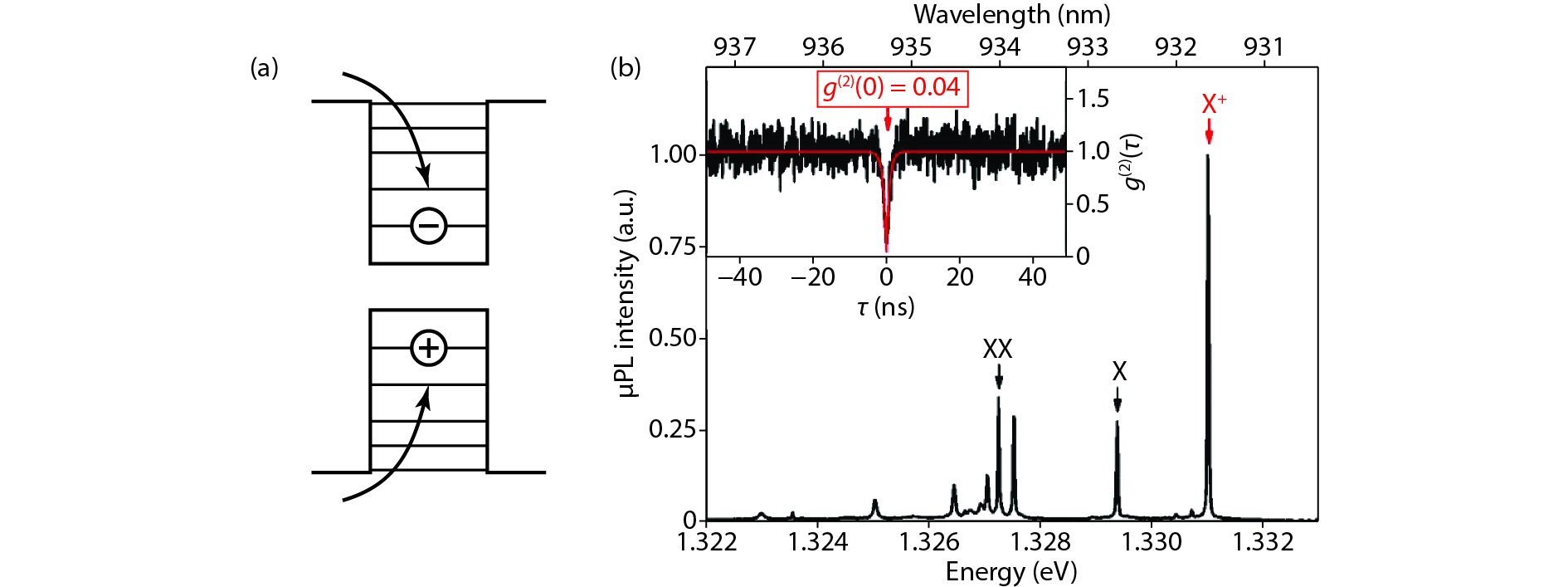
Single-photon emitters (SPEs) are one of the key components in quantum information applications. The ideal SPEs emit a single photon or a photon-pair on demand, with high purity and distinguishability. SPEs can also be integrated in photonic circuits for scalable quantum communication and quantum computer systems. Quantum dots made from III–V compounds such as InGaAs or GaN have been found to be particularly attractive SPE sources due to their well studied optical performance and state of the art industrial flexibility in fabrication and integration. Here, we review the optical and optoelectronic properties and growth methods of general SPEs. Subsequently, a brief summary of the latest advantages in III–V compound SPEs and the research progress achieved in the past few years will be discussed. We finally describe frontier challenges and conclude with the latest SPE fabrication science and technology that can open new possibilities for quantum information applications.
J. Semicond.
2019, 40(7): 072901 doi: 10.1088/1674-4926/40/7/072901
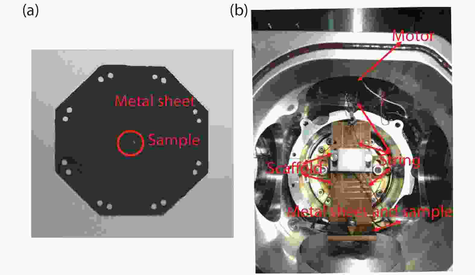
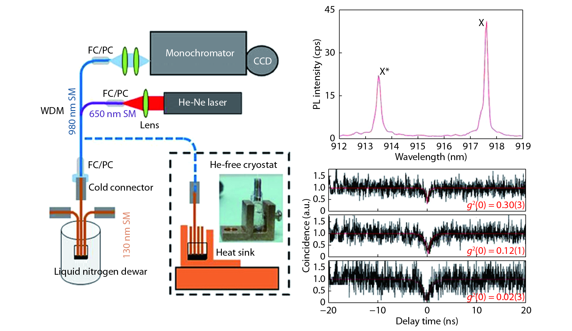
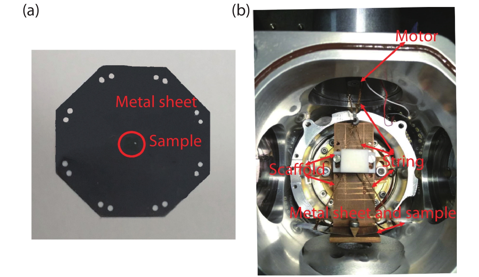
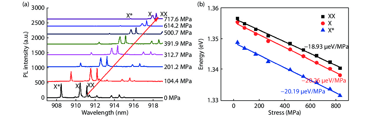
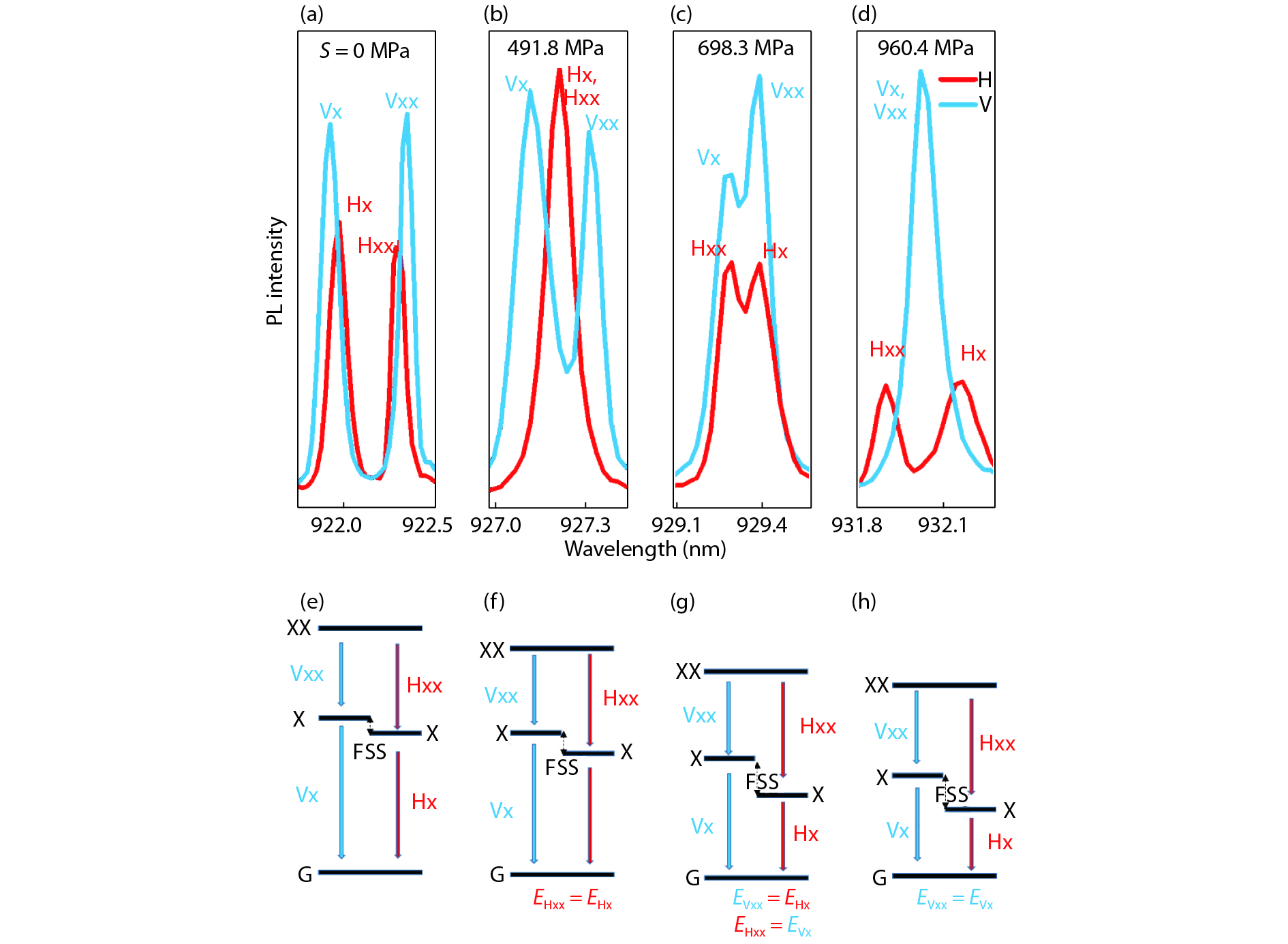
Uniaxial stress is a powerful tool for tuning exciton emitting wavelength, polarization, fine-structure splitting (FSS), and the symmetry of quantum dots (QDs). Here, we present a technique for applying uniaxial stress, which enables us in situ to tune exciton optical properties at low temperature down to 15 K with high tuning precision. The design and operation of the device are described in detail. This technique provides a simple and convenient approach to tune QD structural symmetry, exciton energy and biexciton binding energy. It can be utilized for generating entangled and indistinguishable photons. Moreover, this device can be employed for tuning optical properties of thin film materials at low temperature.


J. Semicond.
2019, 40(7): 072902 doi: 10.1088/1674-4926/40/7/072902
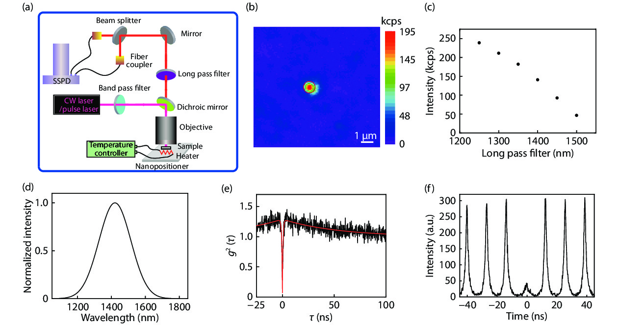
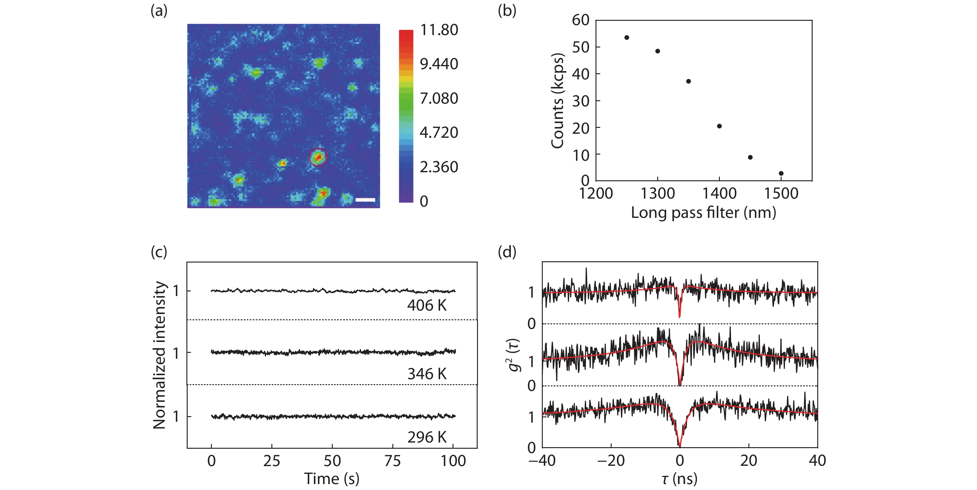
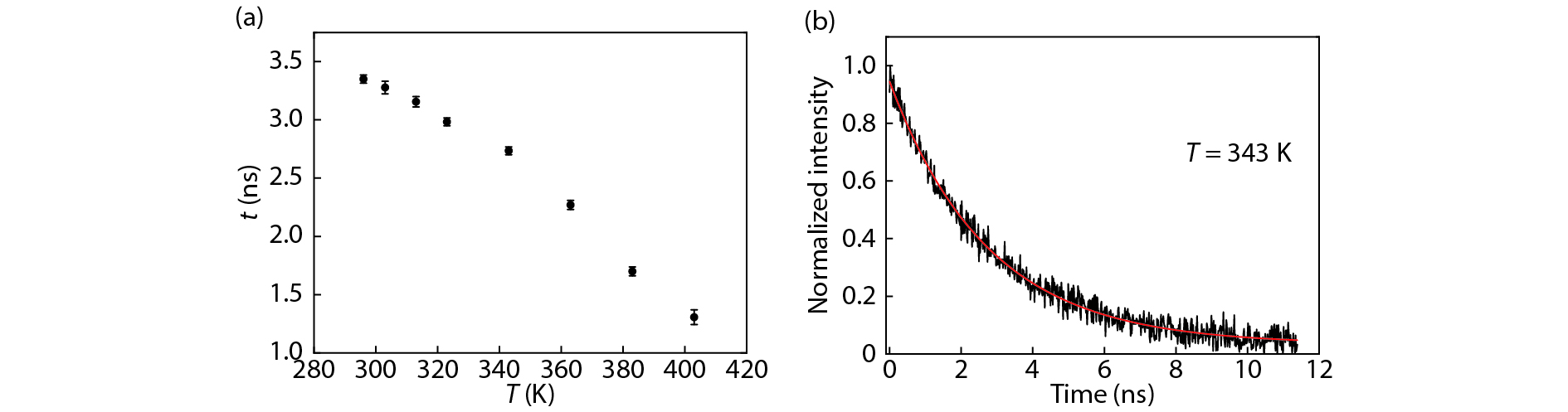
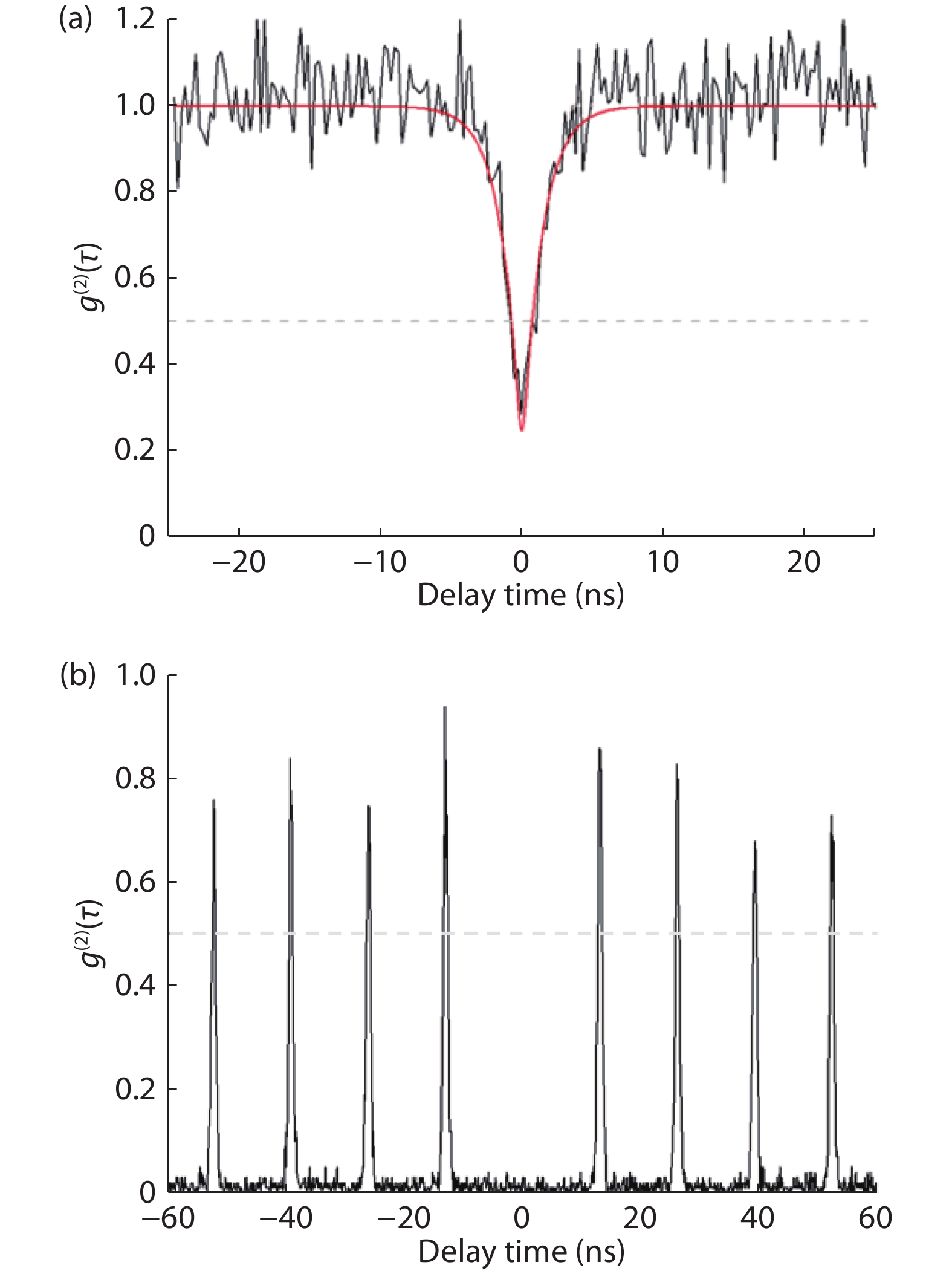
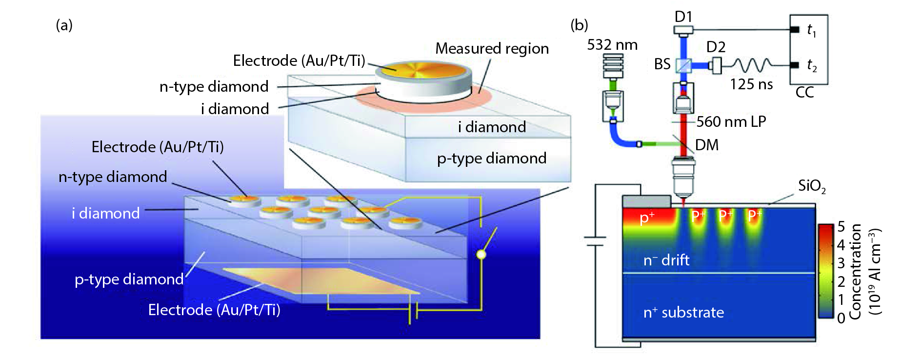
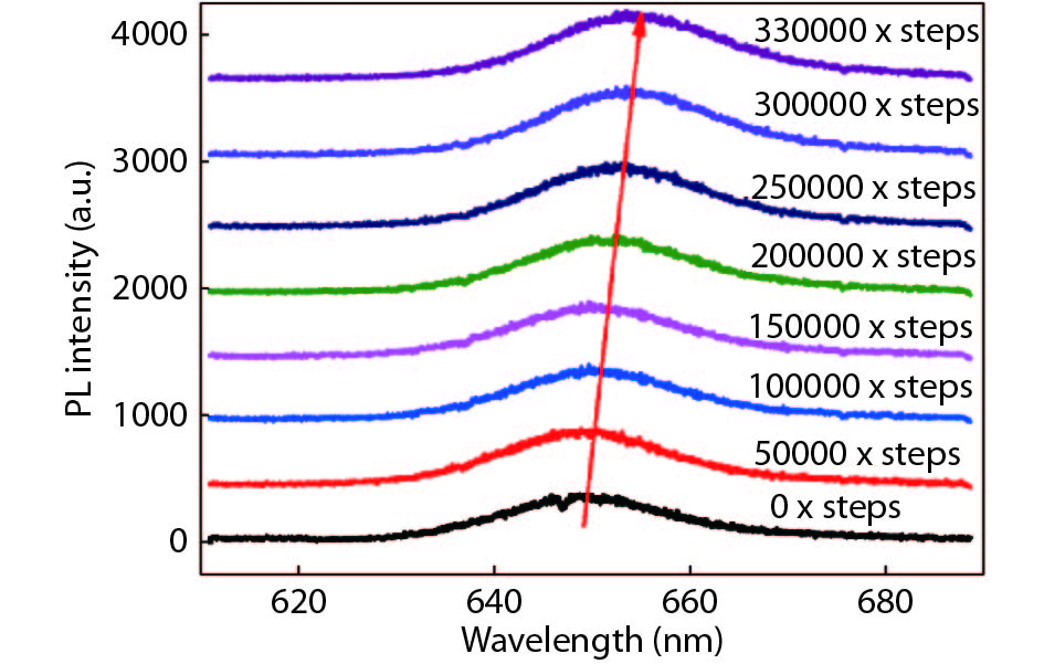
The intrinsic characteristics of single photons became critical issues since the early development of quantum mechanics. Nowadays, acting as flying qubits, single photons are shown to play important roles in the quantum key distribution and quantum networks. Many different single photon sources (SPSs) have been developed. Point defects in silicon carbide (SiC) have been shown to be promising SPS candidates in the telecom range. In this work, we demonstrate a stable SPS in an epitaxial 3C-SiC with the wavelength in the near C-band range, which is very suitable for fiber communications. The observed SPSs show high single photon purity and stable fluorescence at even above 400 K. The lifetimes of the SPSs are found to be almost linearly decreased with the increase of temperature. Since the epitaxial 3C-SiC can be conveniently nanofabricated, these stable near C-band SPSs would find important applications in the integrated photonic devices.