Issue Browser
Volume 43, Issue 7,
Jul 2022
Column
J. Semicond.
2022, 43(7): 071401 doi: 10.1088/1674-4926/43/7/071401
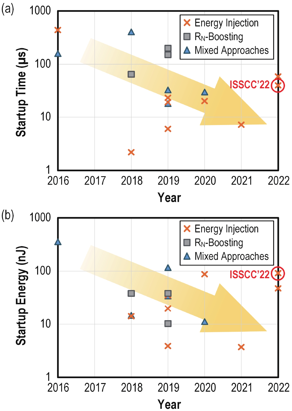
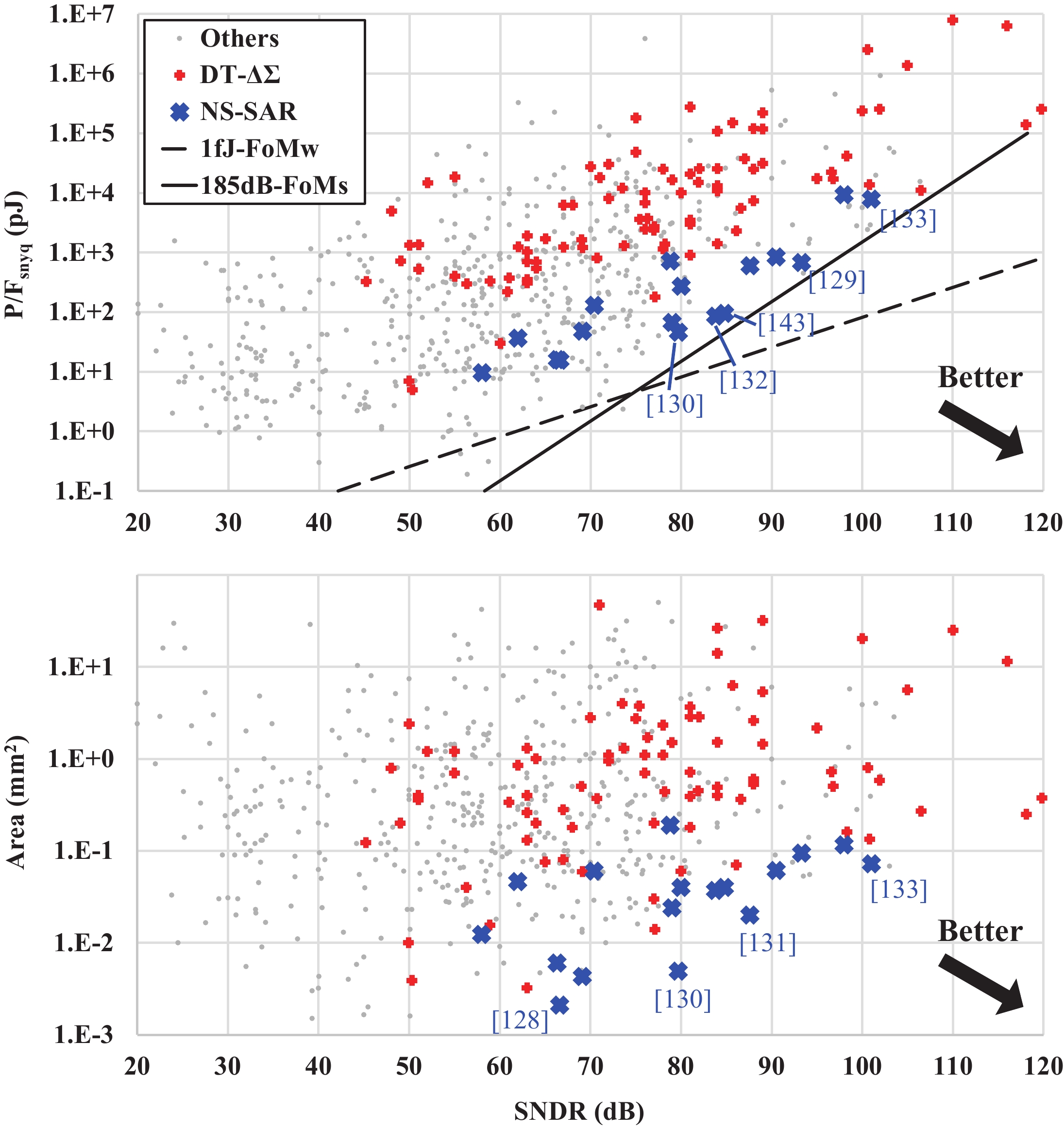
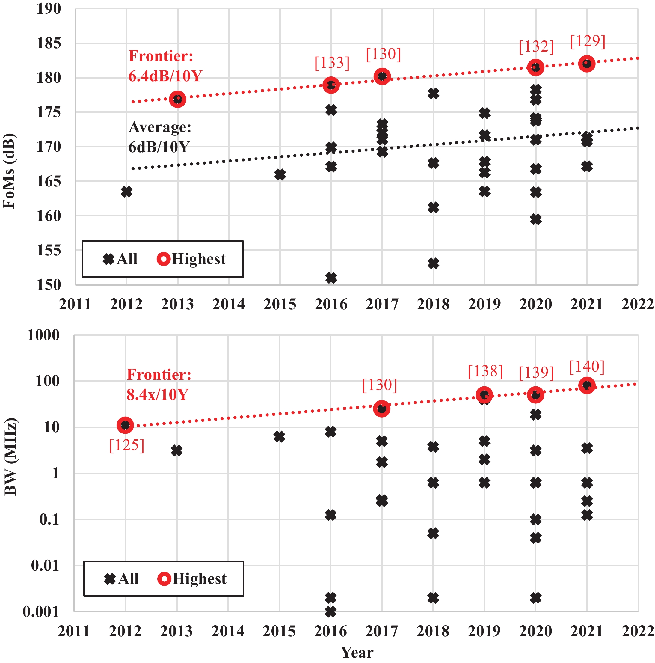
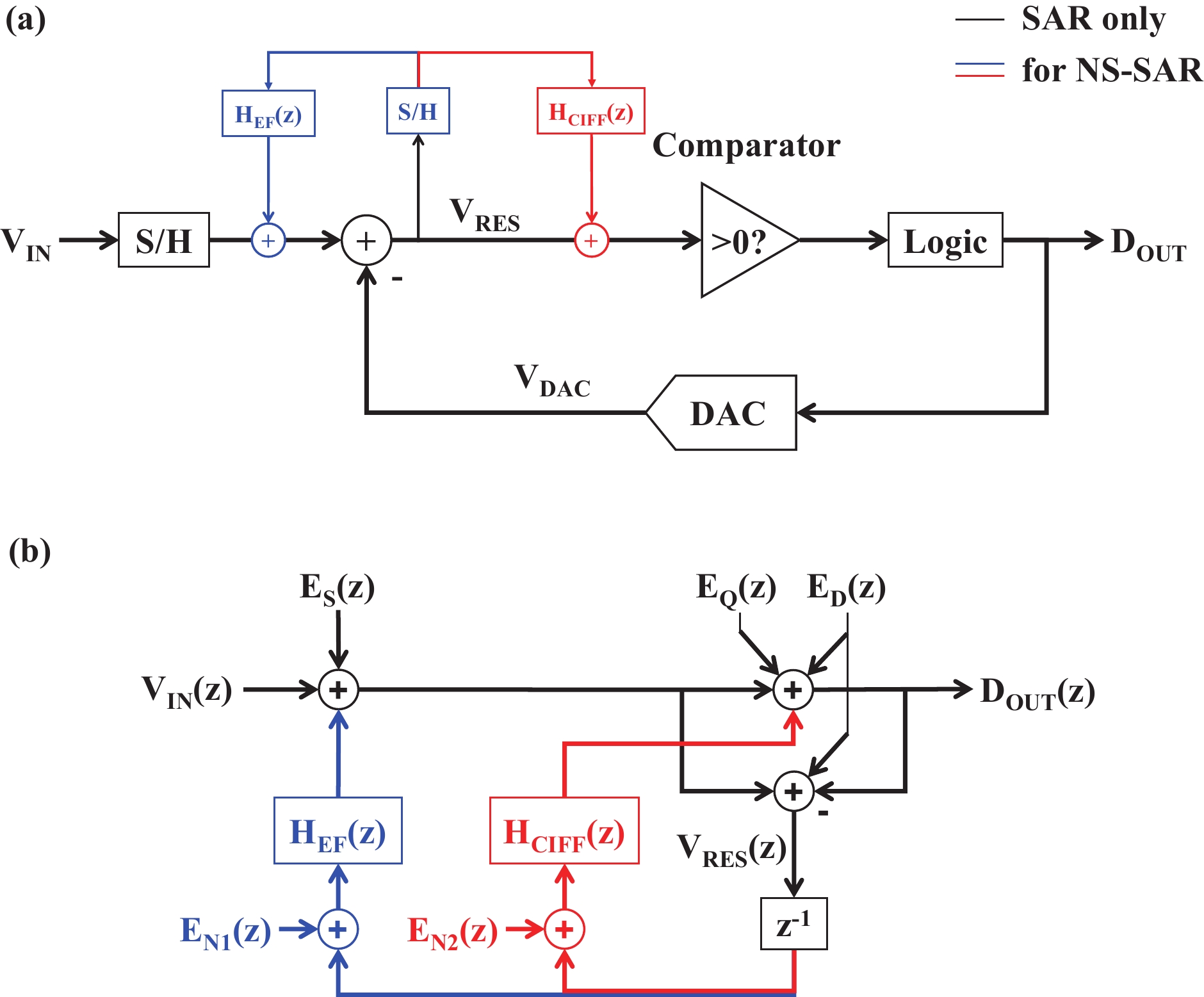
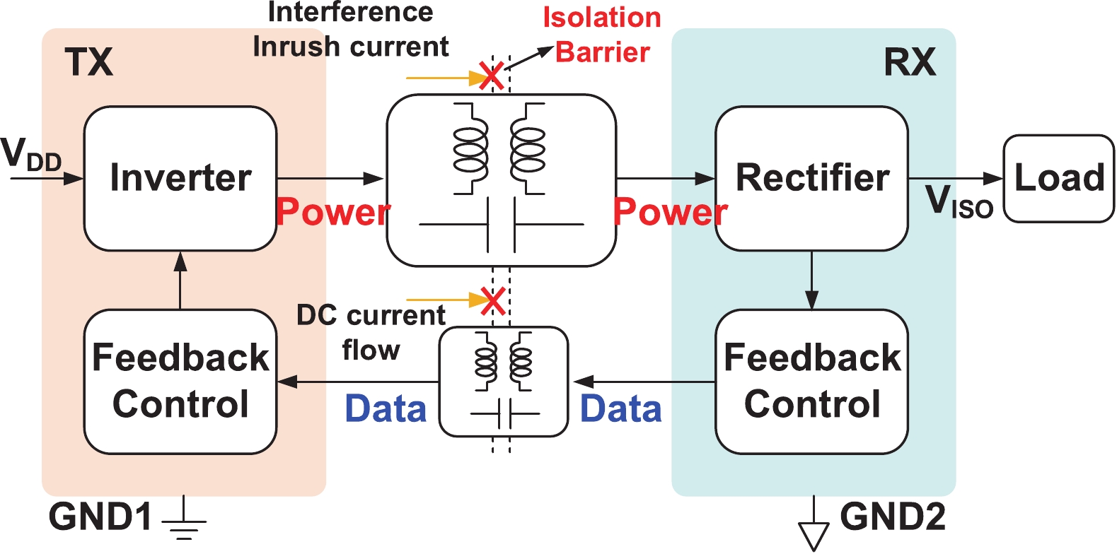
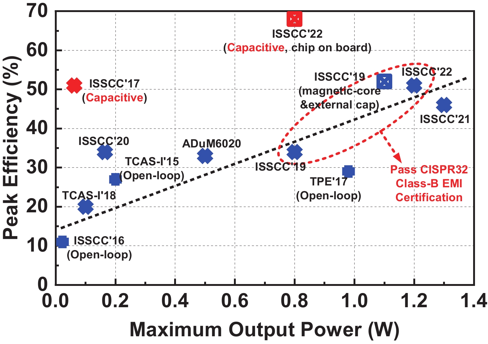
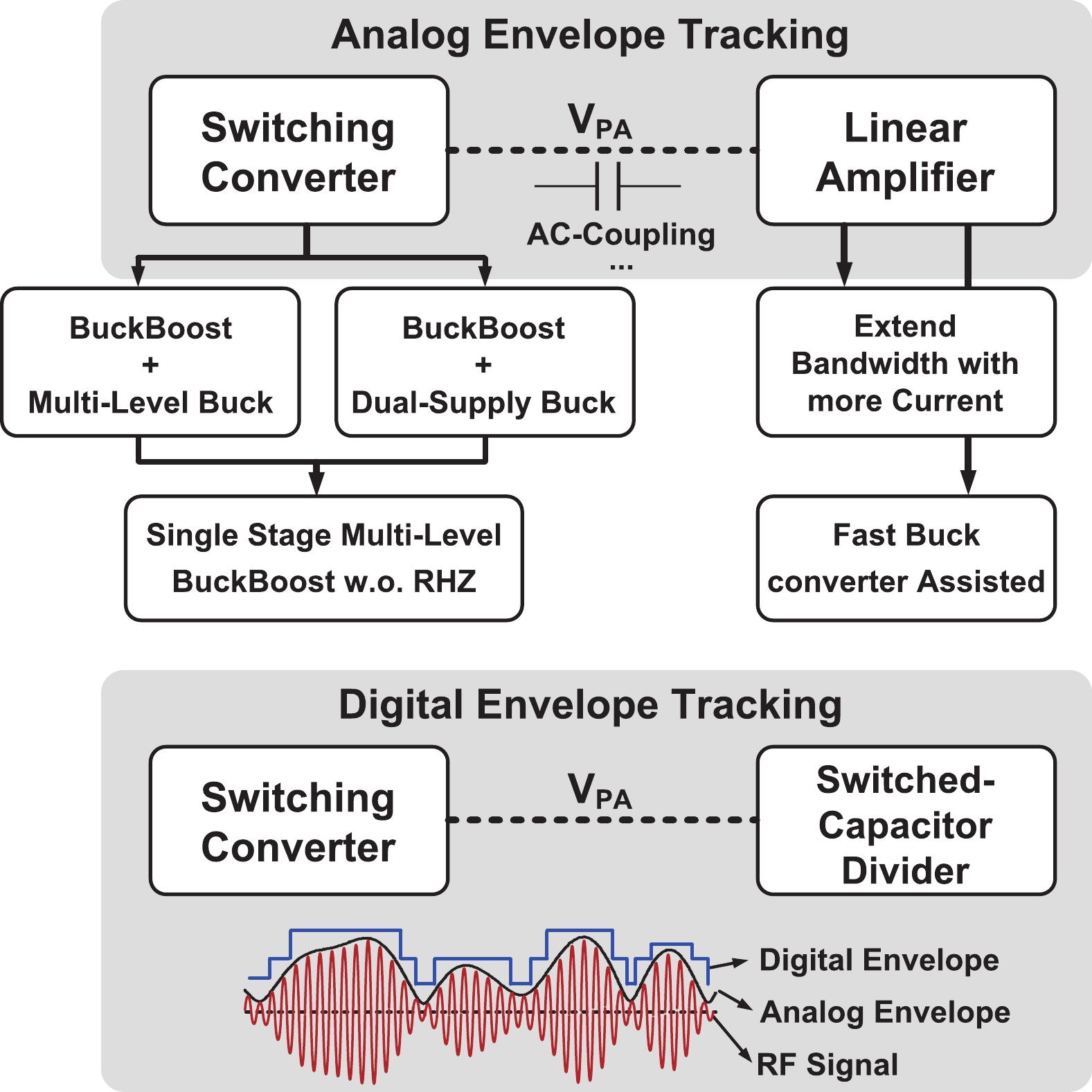
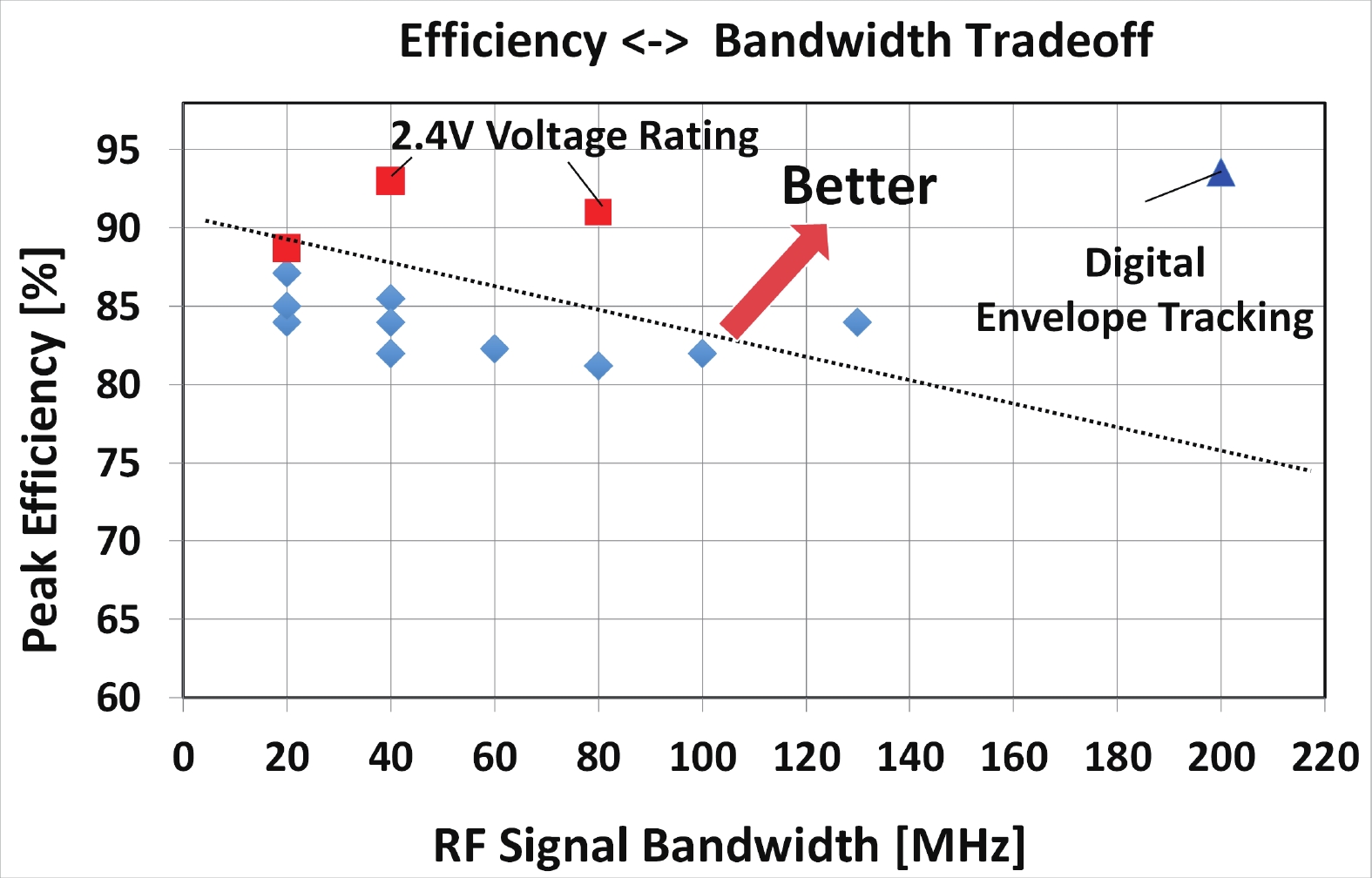
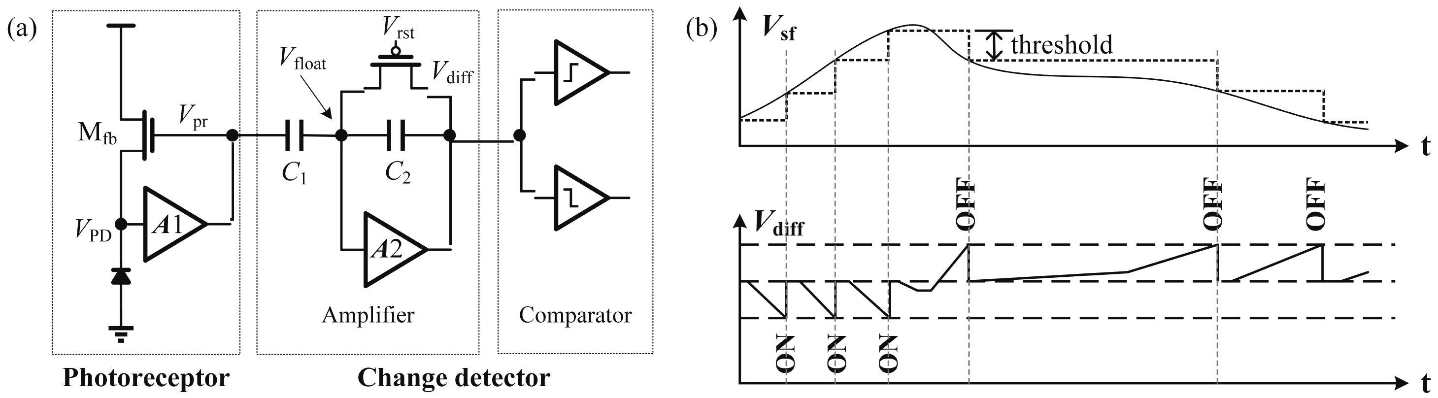
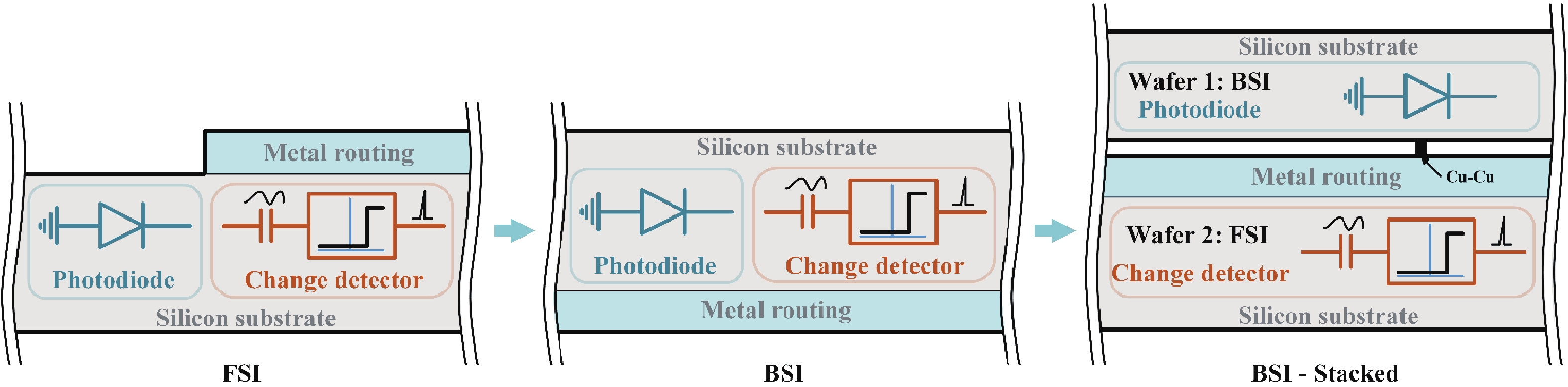
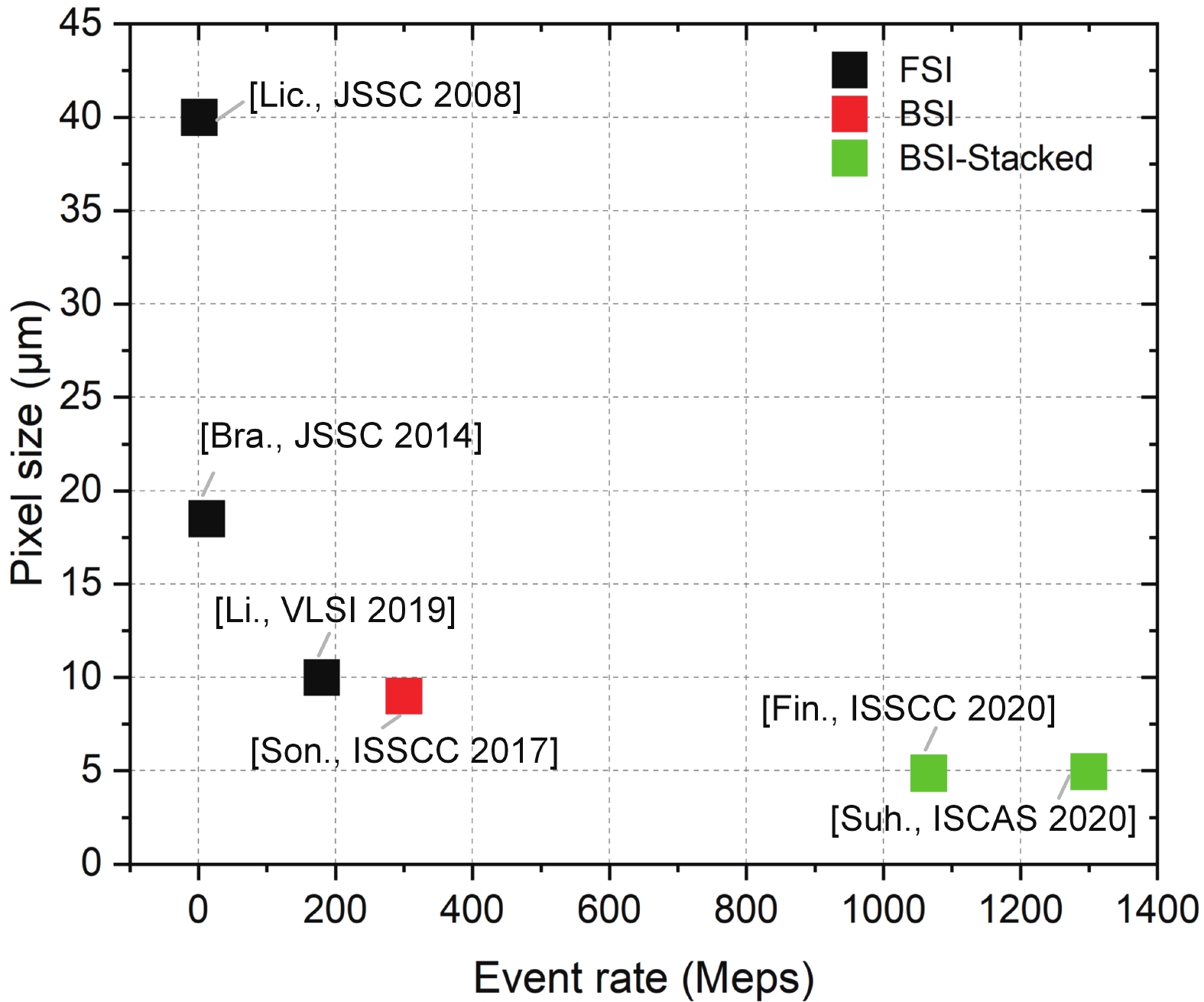
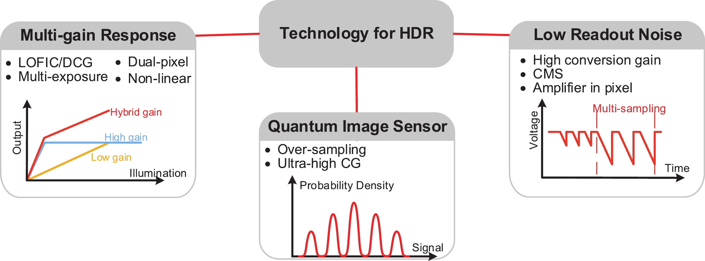
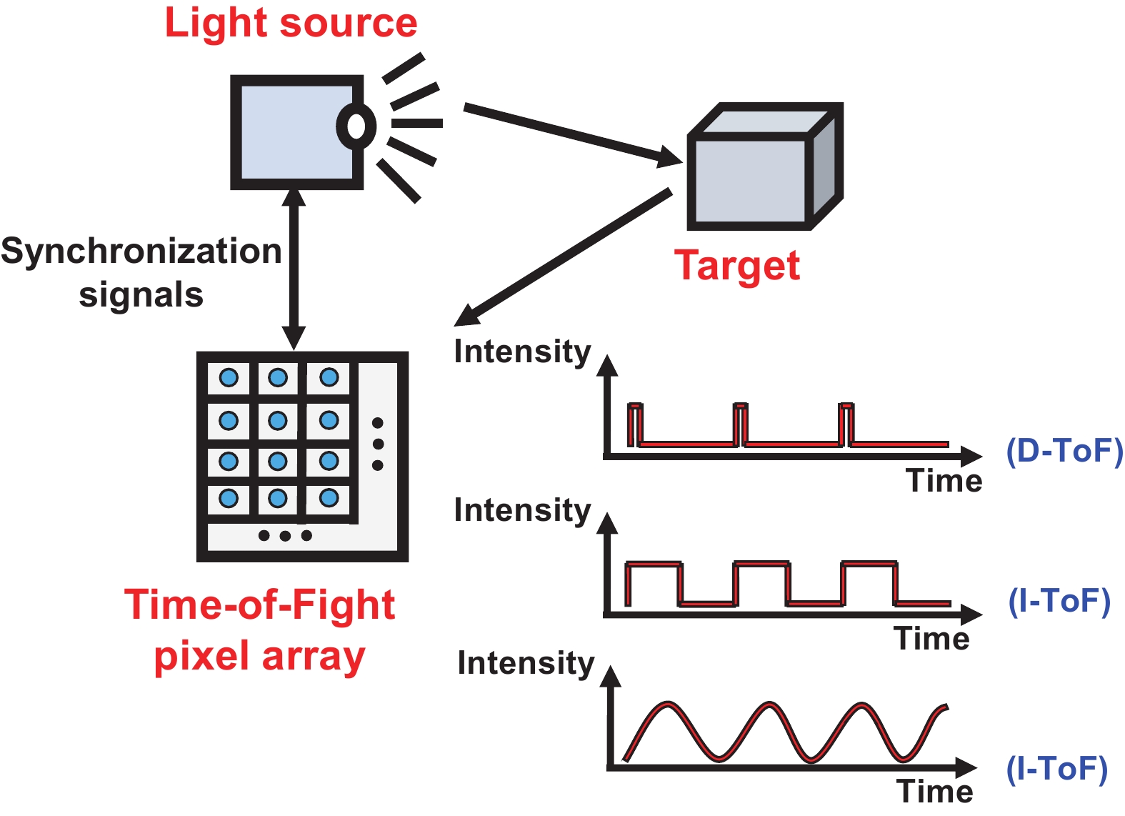
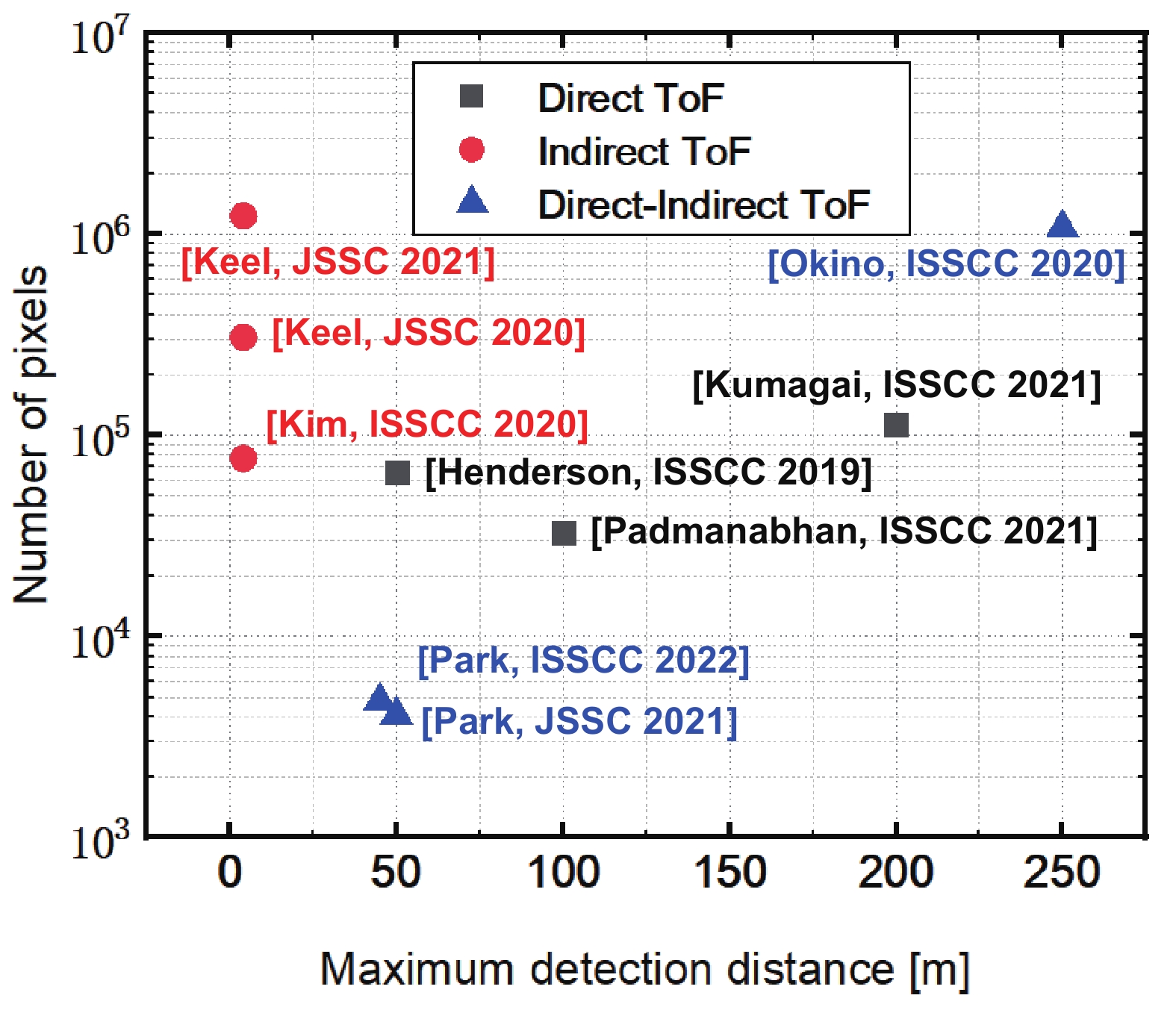
For the non-stop demands for a better and smarter society, the number of electronic devices keeps increasing exponentially; and the computation power, communication data rate, smart sensing capability and intelligence are always not enough. Hardware supports software, while the integrated circuit (IC) is the core of hardware. In this long review paper, we summarize and discuss recent trending IC design directions and challenges, and try to give the readers big/cool pictures on each selected small/hot topics. We divide the trends into the following six categories, namely, 1) machine learning and artificial intelligence (AI) chips, 2) communication ICs, 3) data converters, 4) power converters, 5) imagers and range sensors, 6) emerging directions. Hope you find this paper useful for your future research and works.


J. Semicond.
2022, 43(7): 072101 doi: 10.1088/1674-4926/43/7/072101

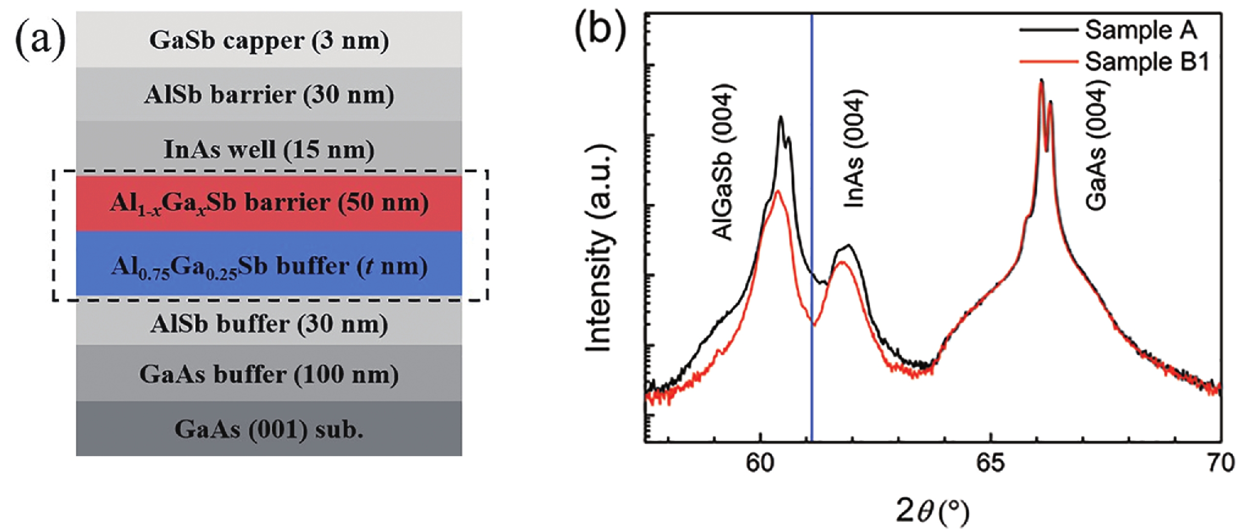
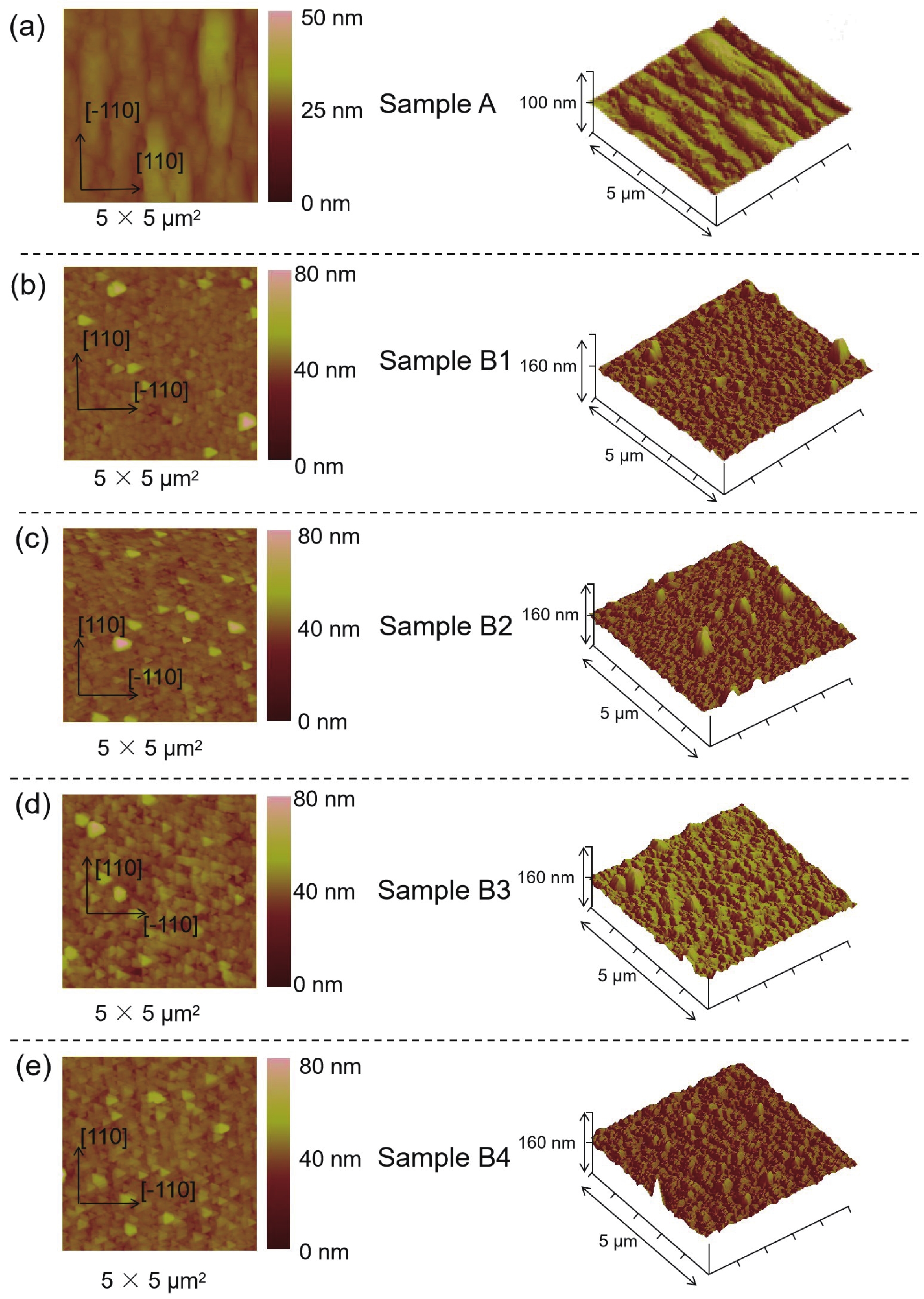
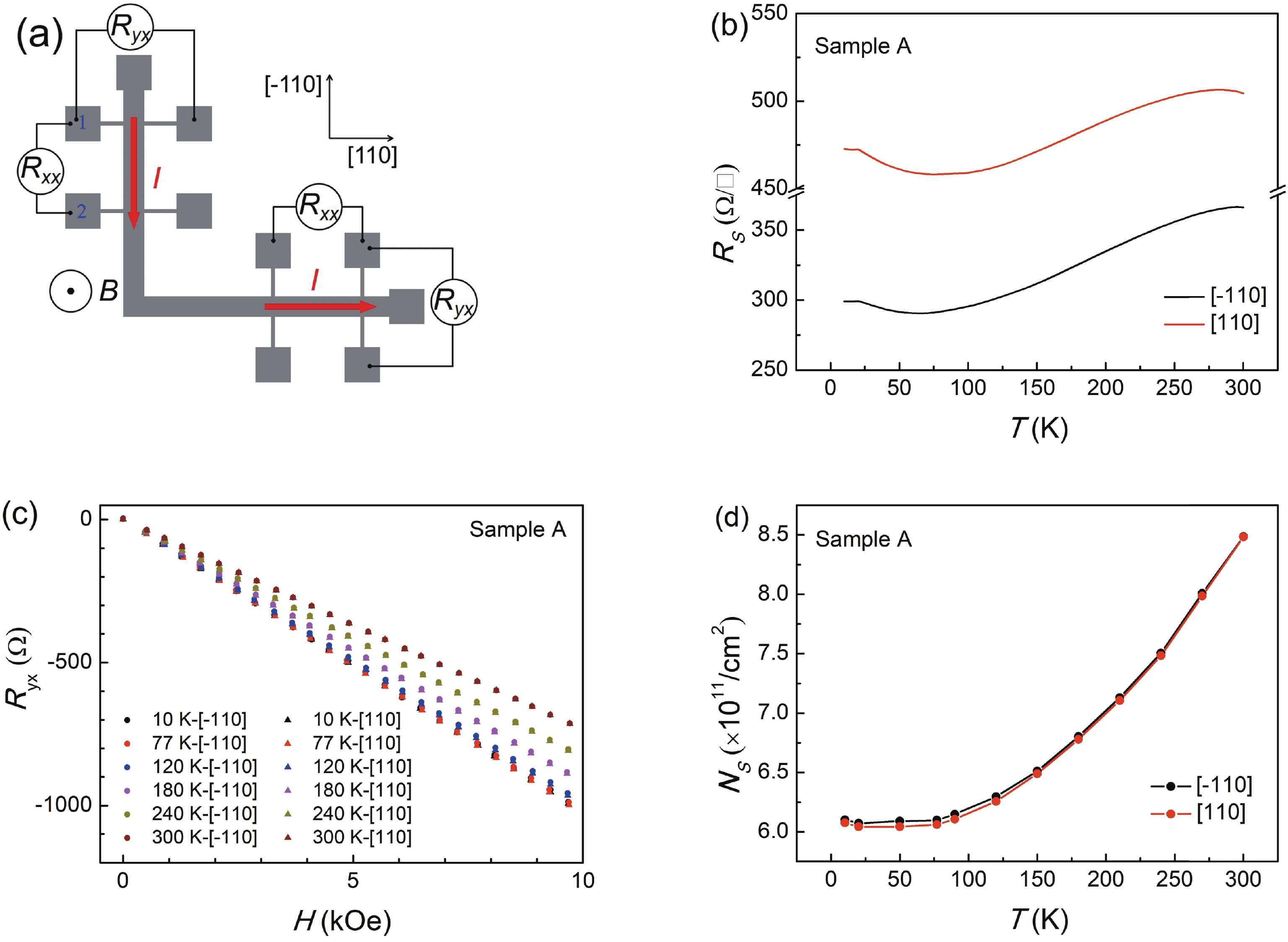
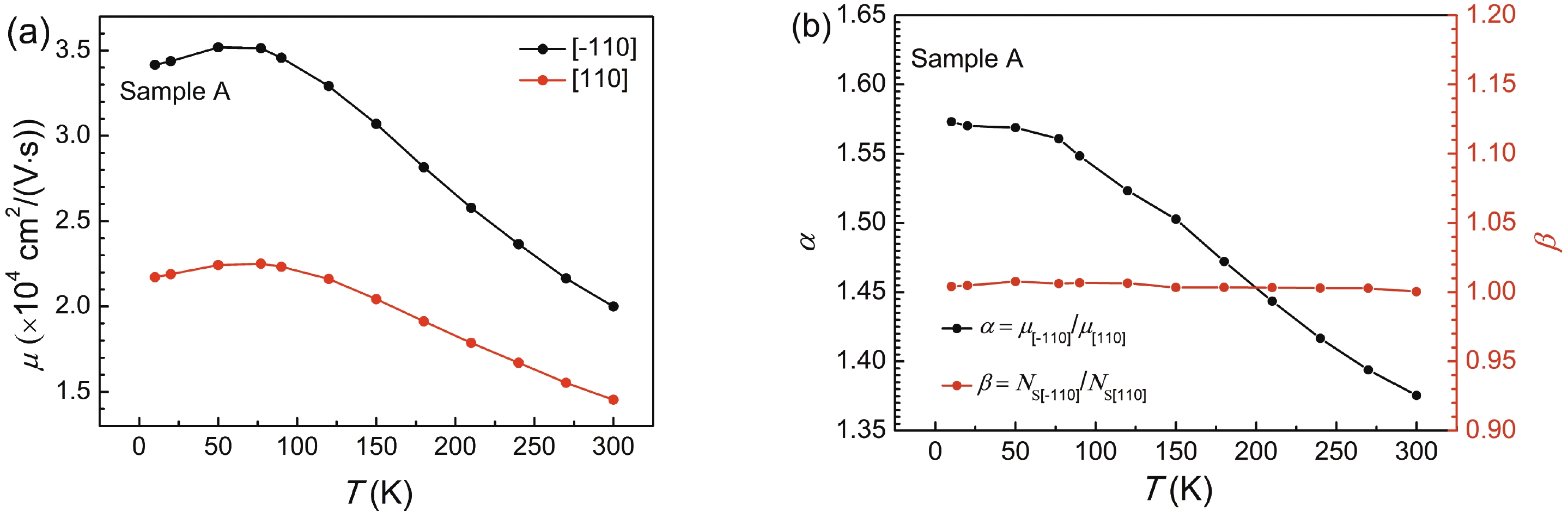
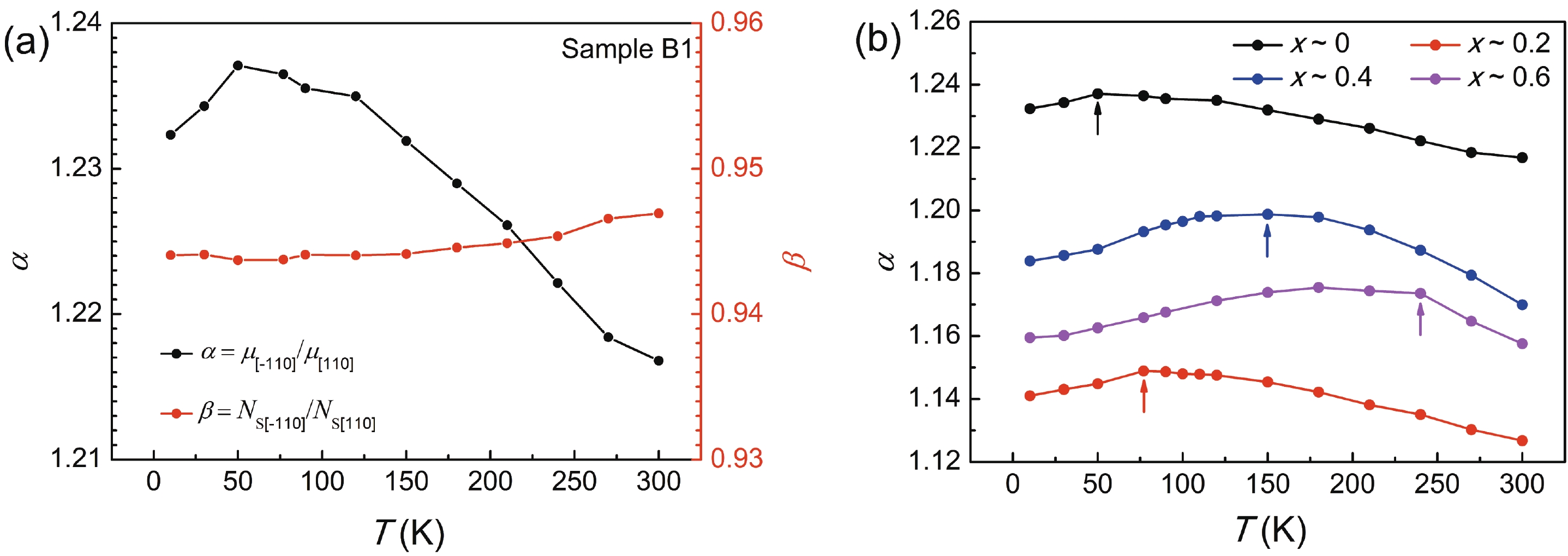
The electron mobility anisotropy in (Al,Ga)Sb/InAs two-dimensional electron gases with different surface morphology has been investigated. Large electron mobility anisotropy is found for the sample with anisotropic morphology, which is mainly induced by the threading dislocations in the InAs layer. For the samples with isotropic morphology, the electron mobility is also anisotropic and could be attributed to the piezoelectric scattering. At low temperature (below transition temperature), the piezoelectric scattering is enhanced with the increase of temperature, leading to the increase of electron mobility anisotropy. At high temperature (above transition temperature), the phonon scattering becomes dominant. Because the phonon scattering is isotropic, the electron mobility anisotropy in all the samples would be reduced. Our results provide useful information for the comprehensive understanding of electron mobility anisotropy in the (Al,Ga)Sb/InAs system.
J. Semicond.
2022, 43(7): 072301 doi: 10.1088/1674-4926/43/7/072301

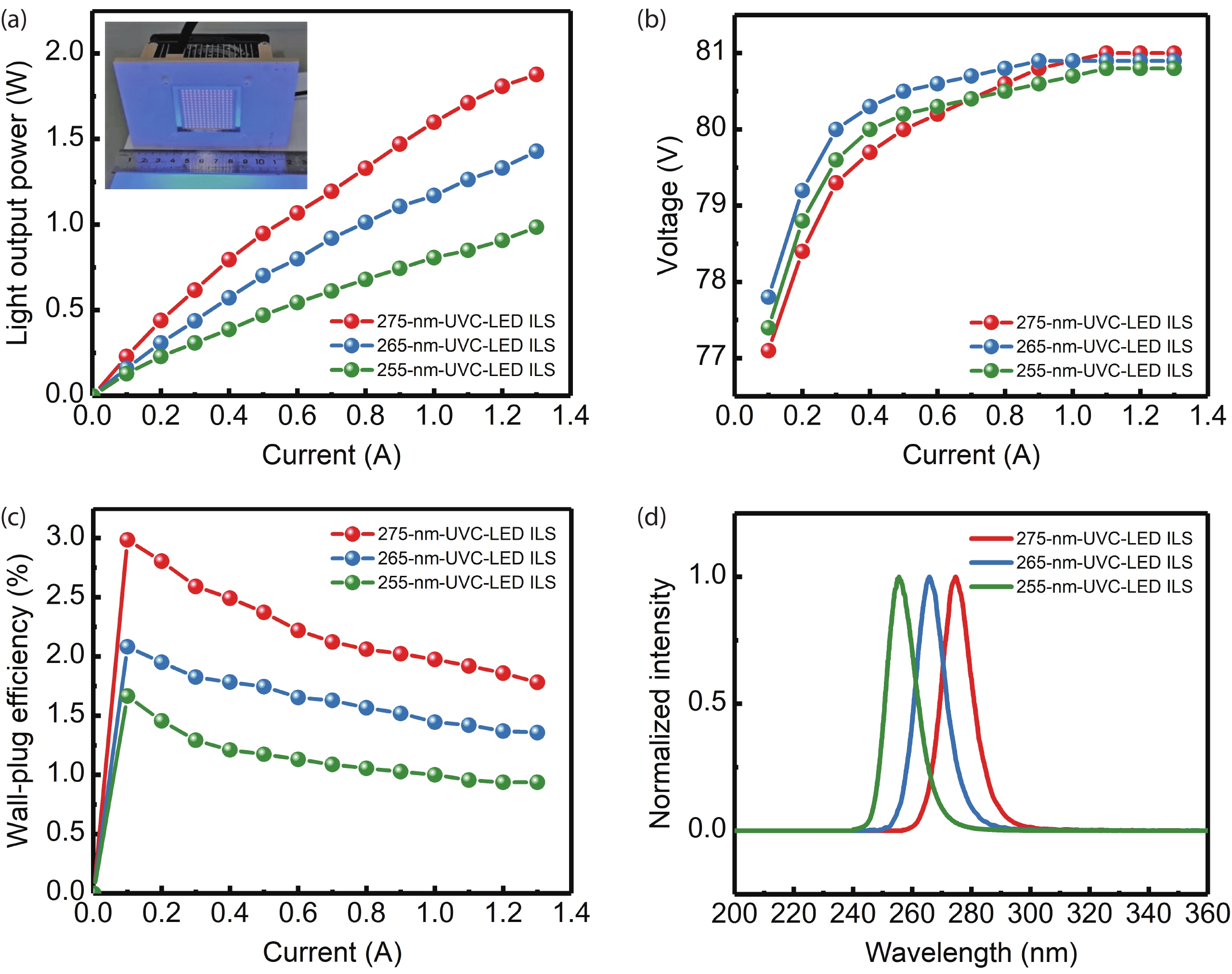
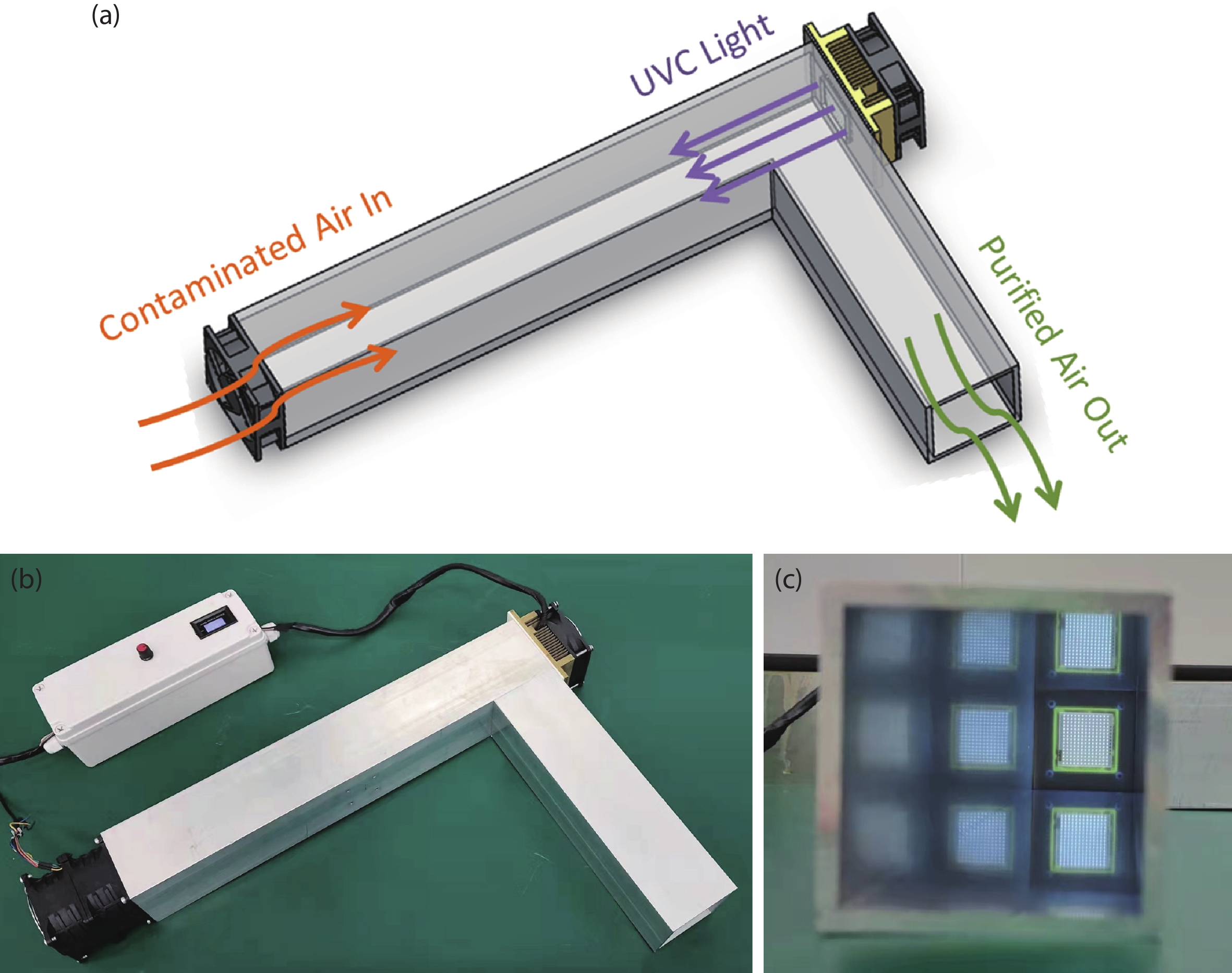
With the epidemic of the coronavirus disease (COVID-19) infection, AlGaN-based ultraviolet-C light emitting diodes (UVC-LEDs) have attracted widespread attention for their sterilization application. However, the sterilization characters of high power integrated light sources (ILSs) haven’t been widely investigated before utilizing in public sanitary security. In this work, by integrating up to 195 UVC-LED chips, high power UVC-LED ILSs with a light output power (LOP) of 1.88 W were demonstrated. The UVC-LED ILSs were verified to have efficient and rapid sterilization capability, which have achieved more than 99.9% inactivation rate of several common pathogenic microorganisms within 1 s. In addition, the corresponding air sterilization module based on them was also demonstrated to kill more than 97% of Staphylococcus albus in the air of 20 m3 confined room within 30 min. This work demonstrates excellent sterilization ability of UVC-LED ILSs with high LOP, revealing great potential of UVC-LEDs in sterilization applications in the future.


J. Semicond.
2022, 43(7): 072401 doi: 10.1088/1674-4926/43/7/072401
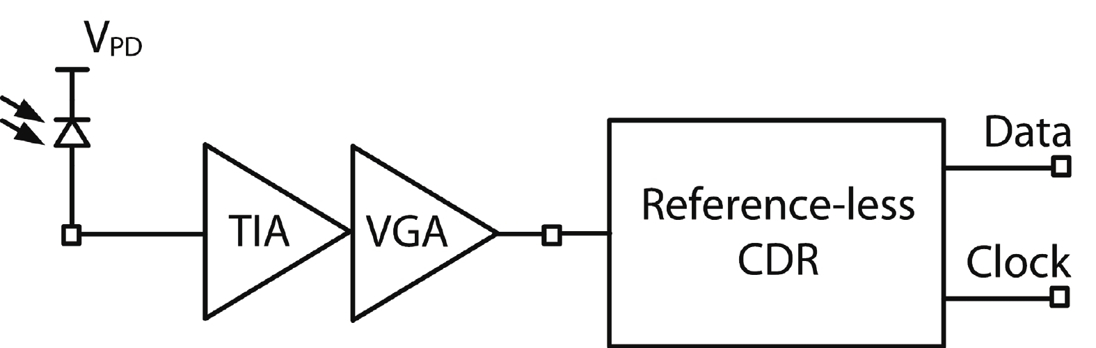
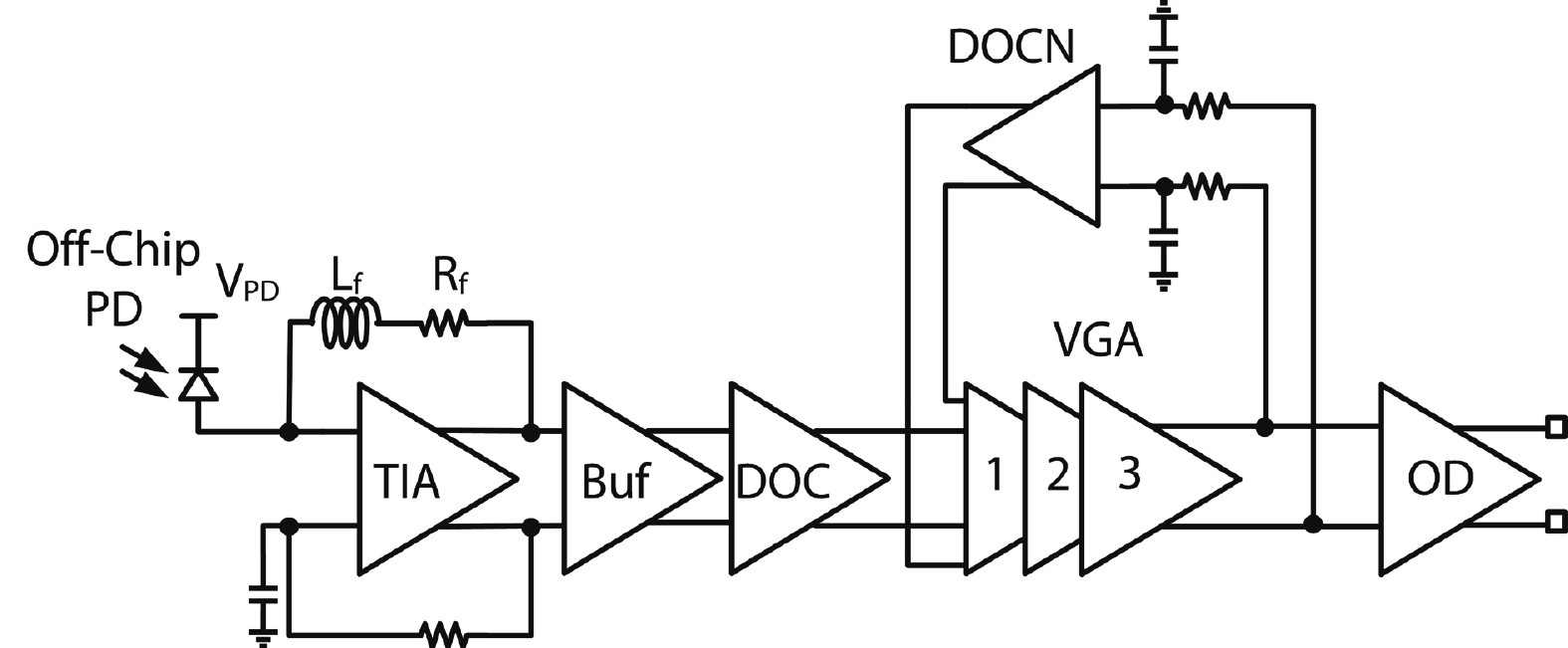
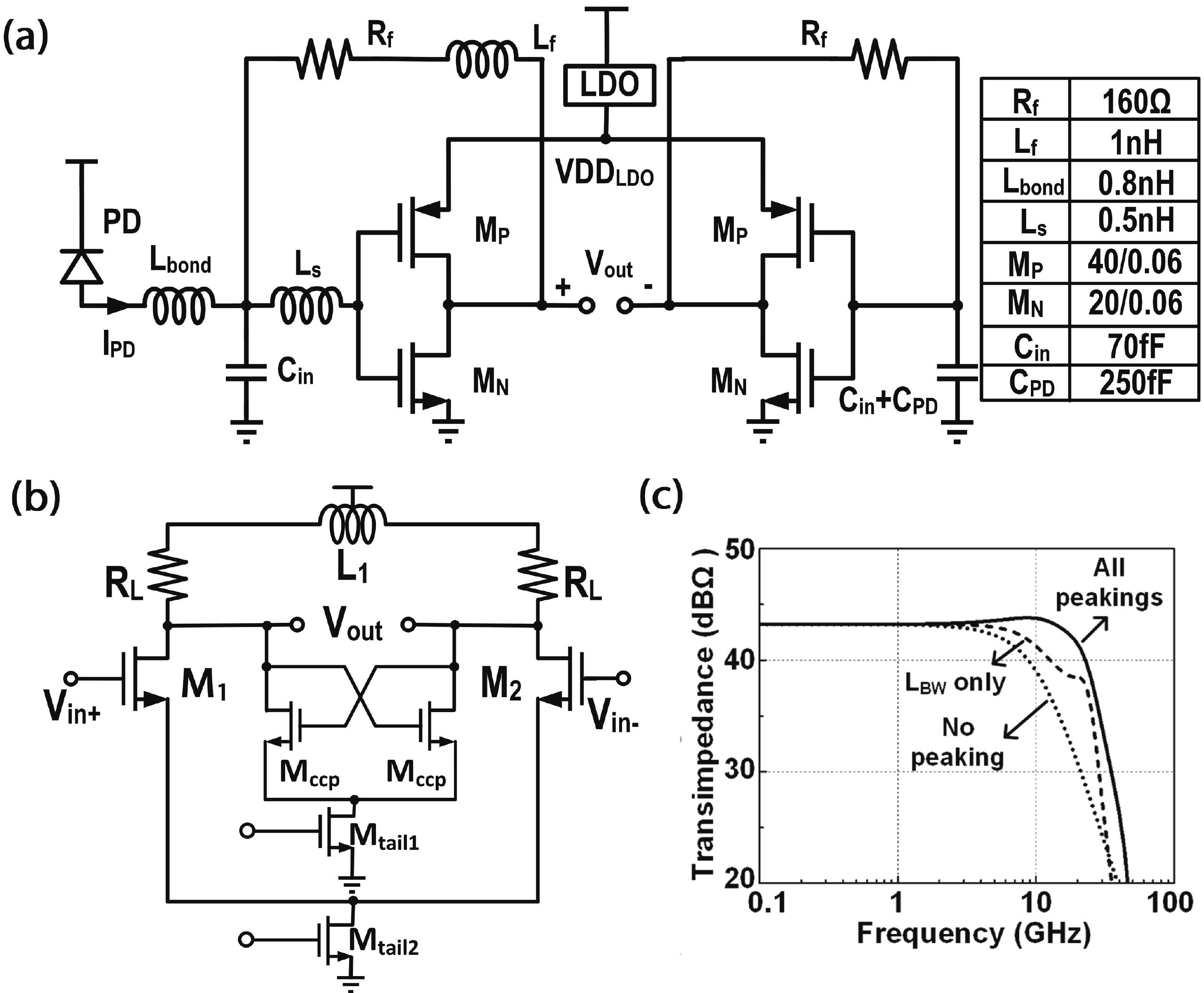
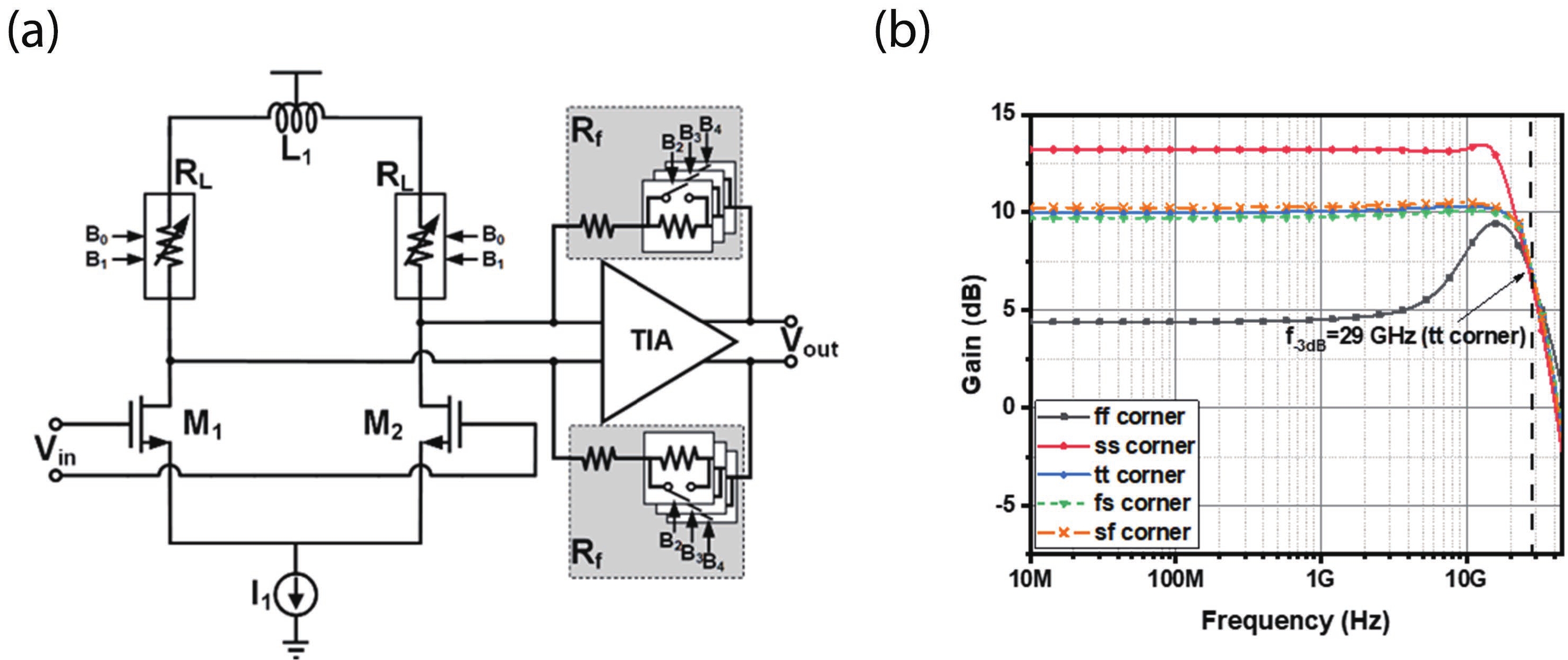
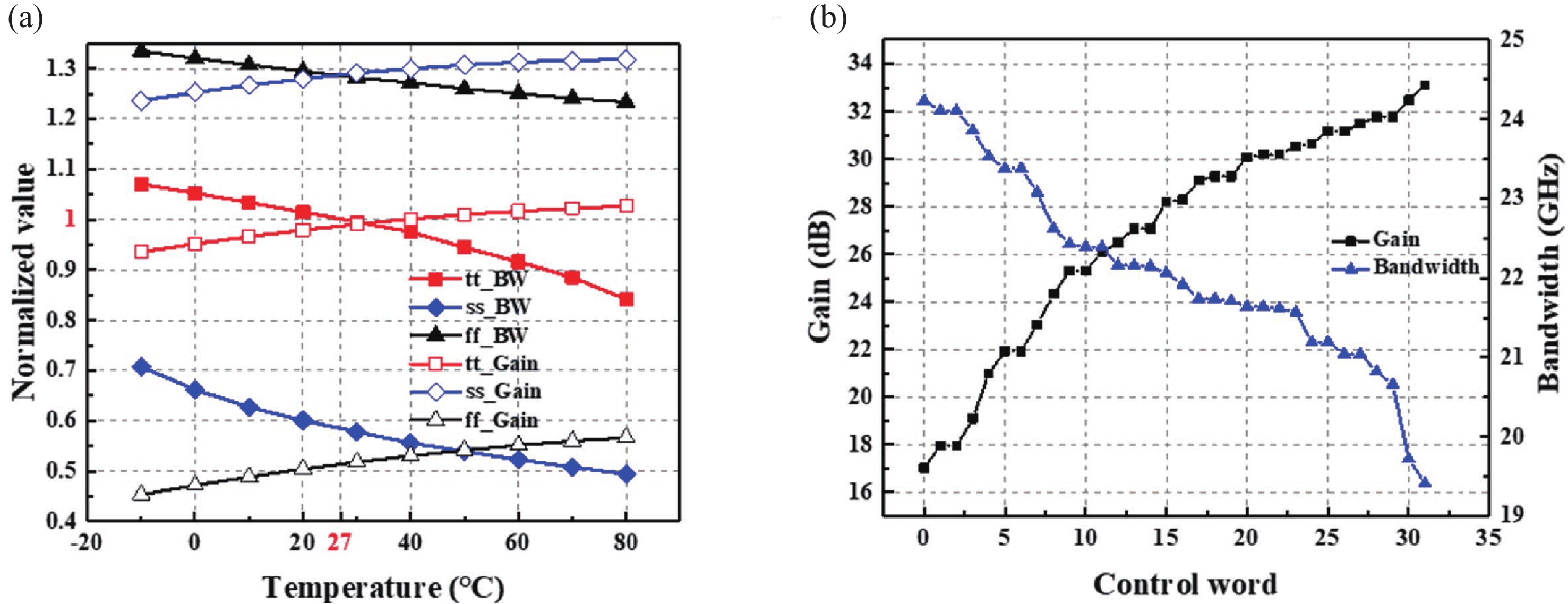
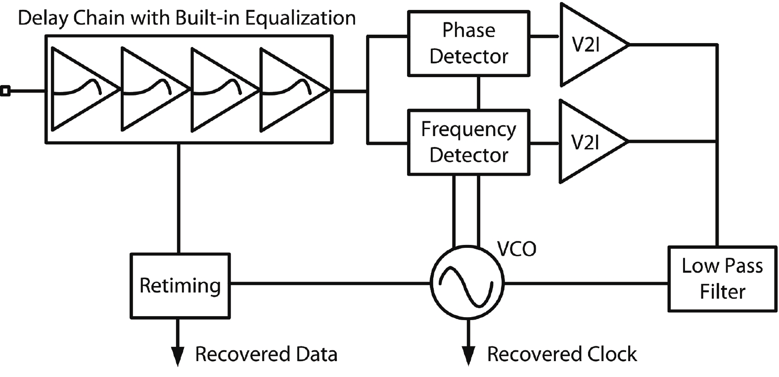
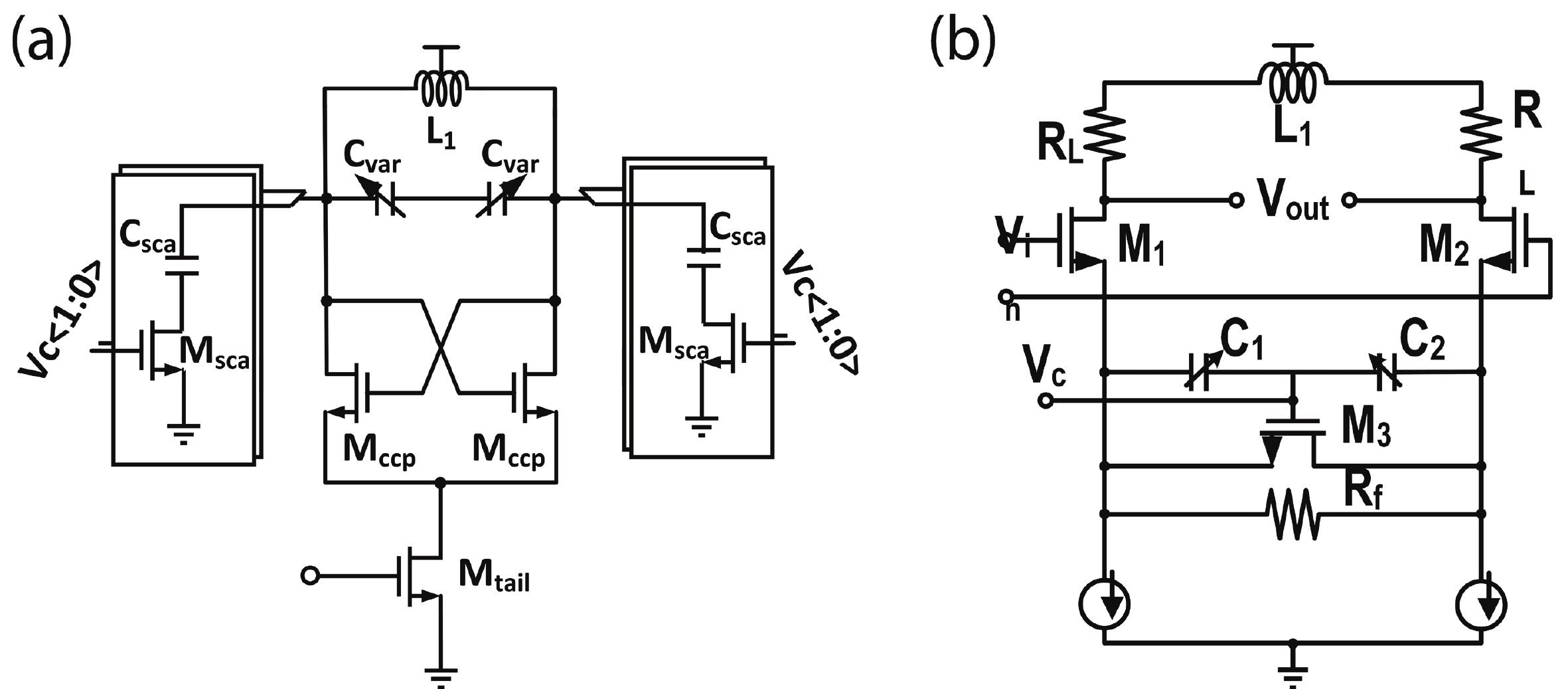
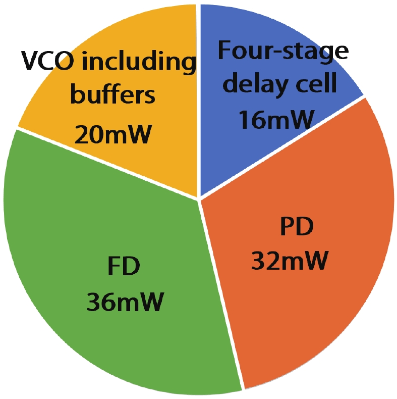
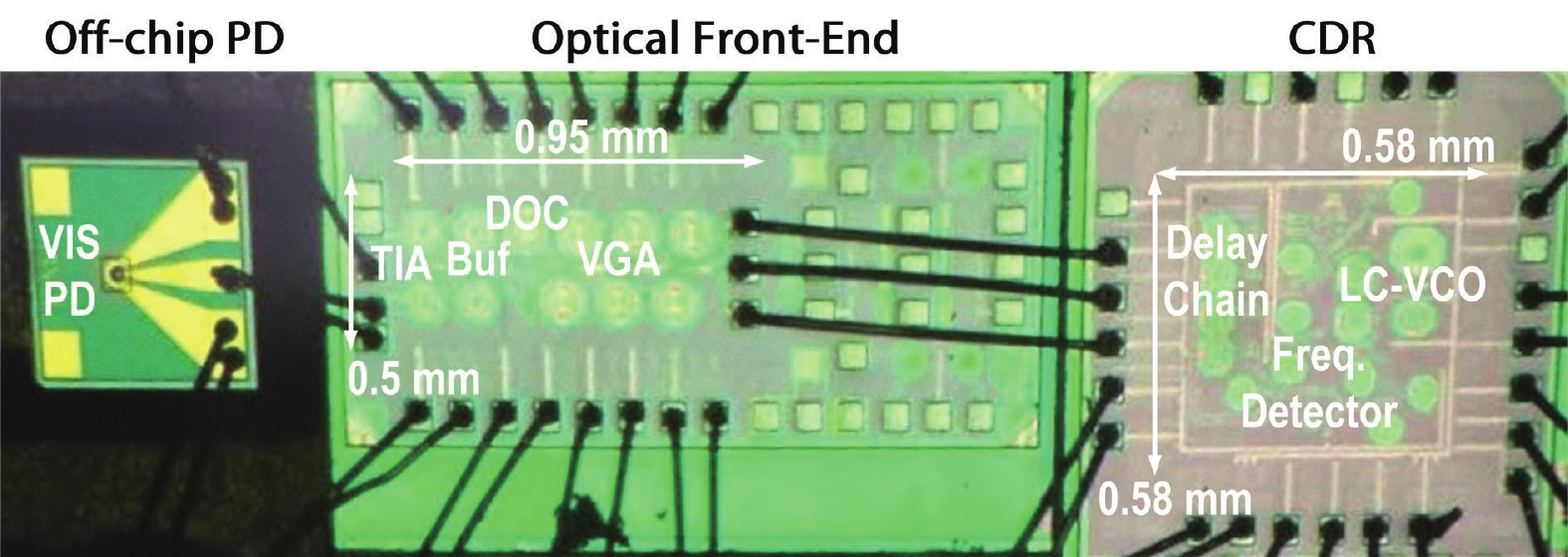
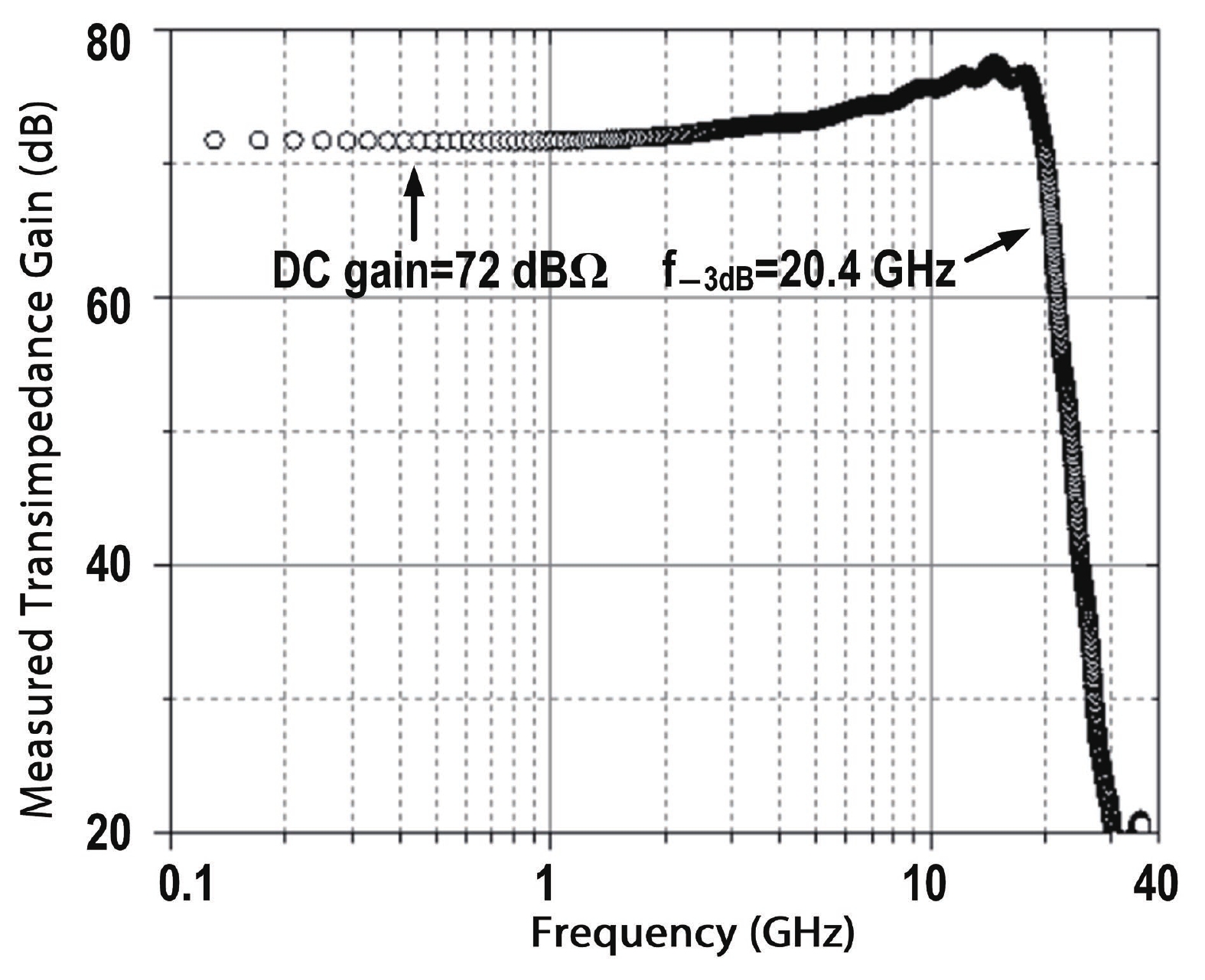
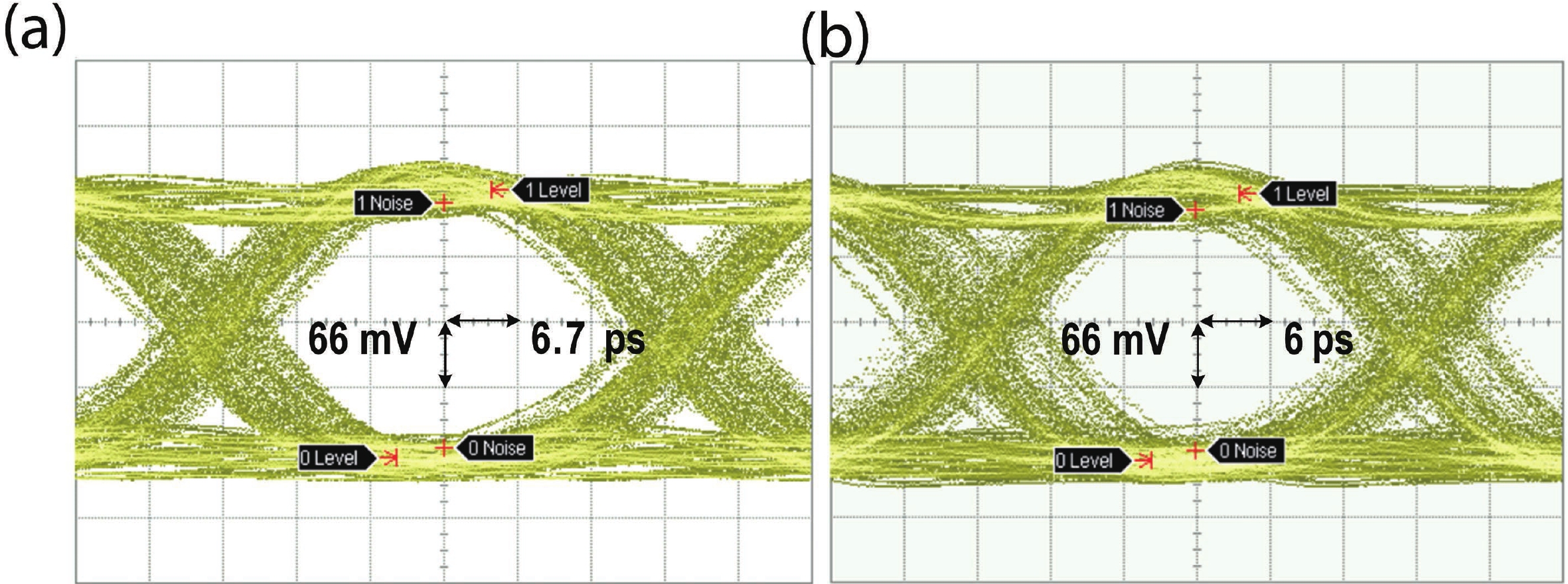
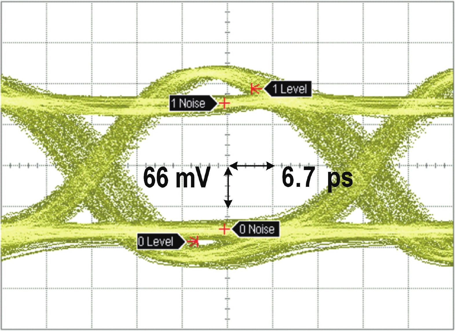
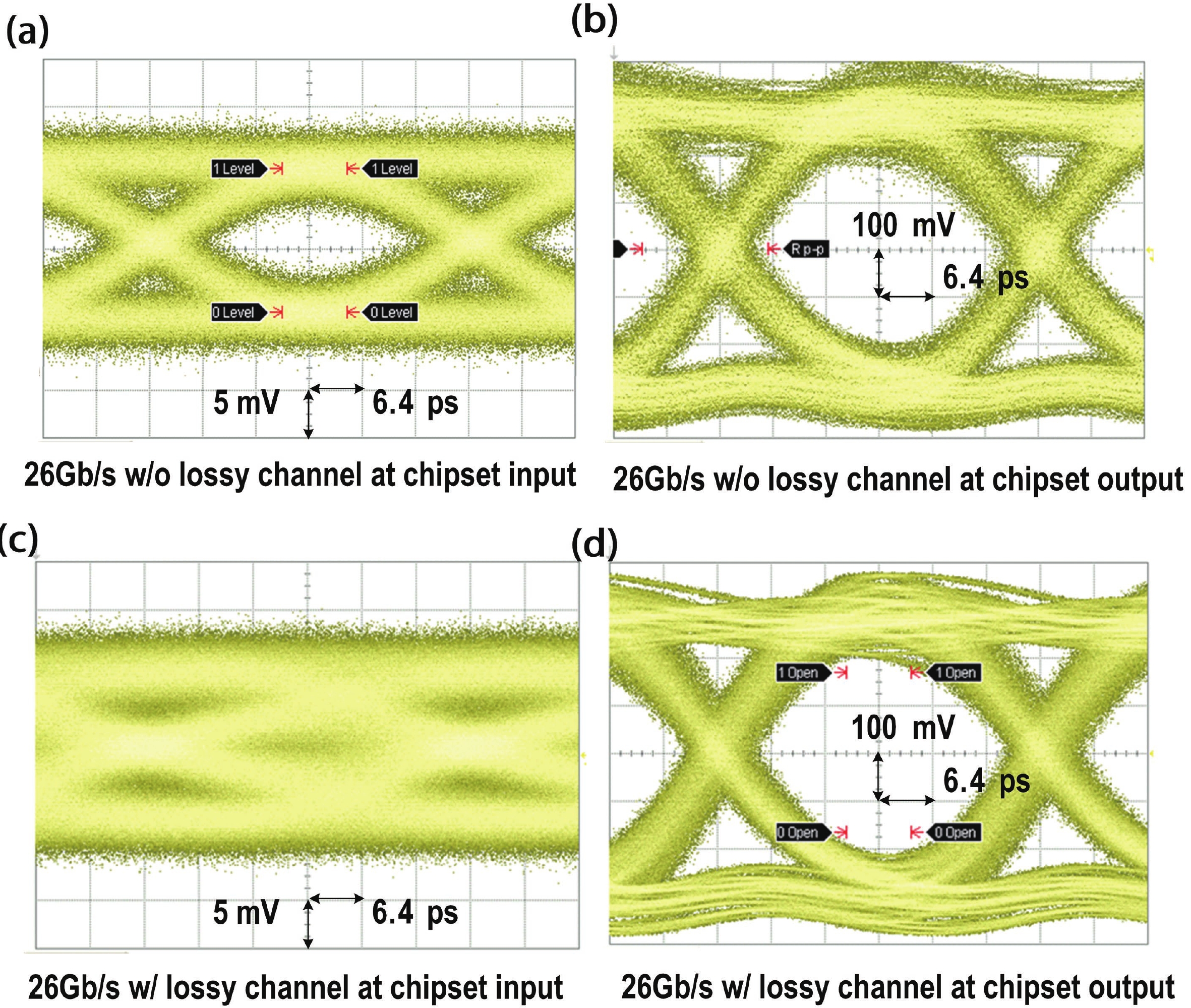
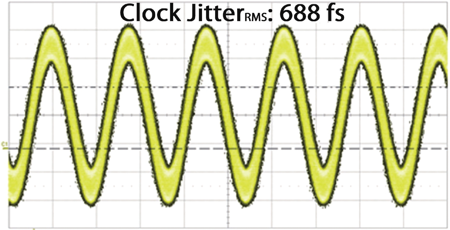
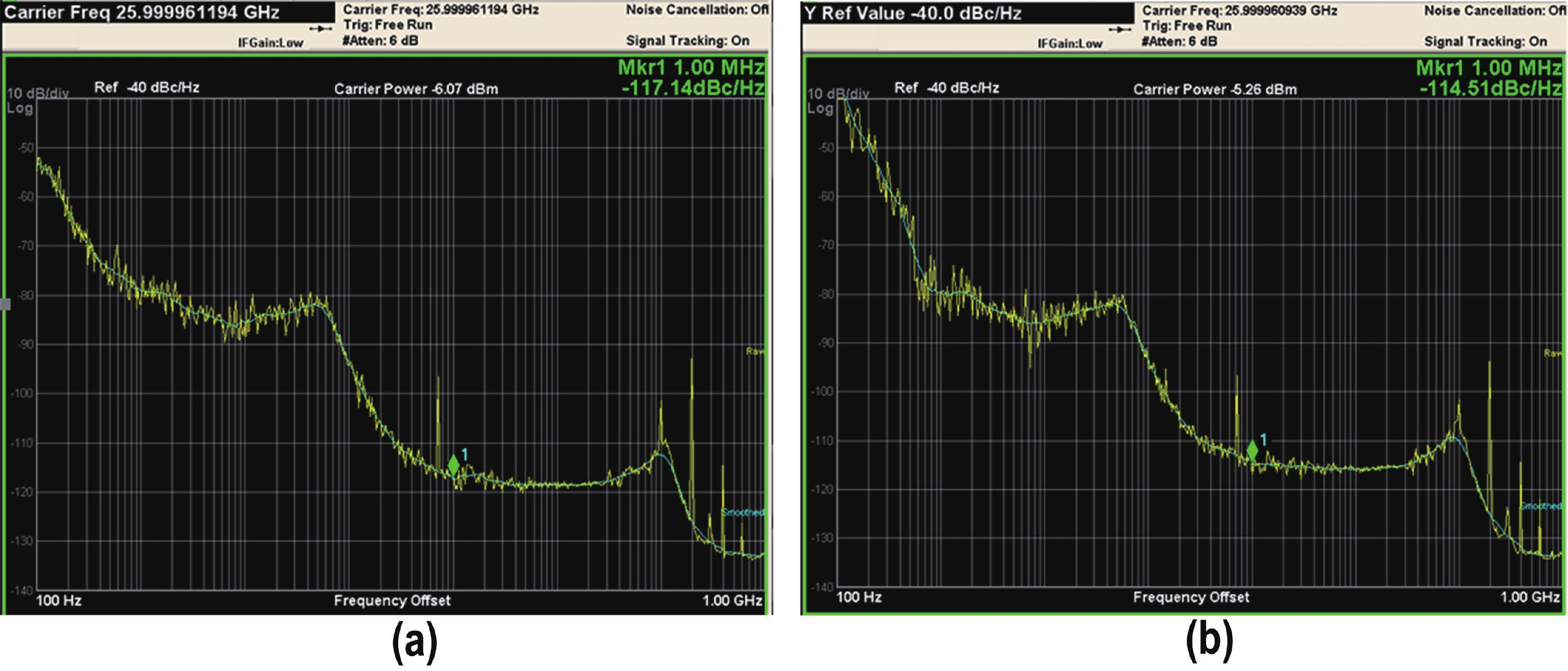
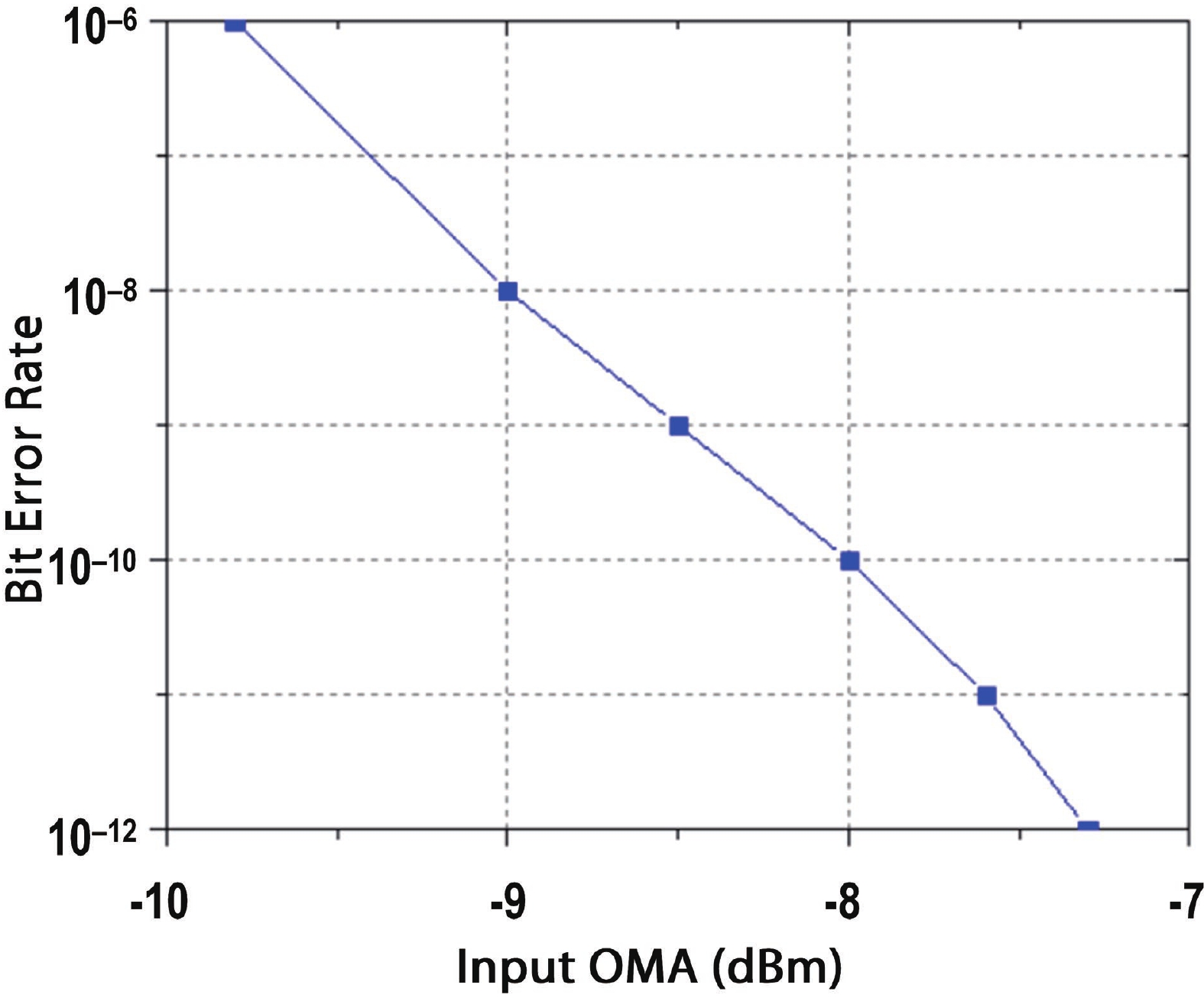
This paper presents a 26-Gb/s CMOS optical receiver that is fabricated in 65-nm technology. It consists of a triple-inductive transimpedance amplifier (TIA), direct current (DC) offset cancellation circuits, 3-stage gm-TIA variable-gain amplifiers (VGA), and a reference-less clock and data recovery (CDR) circuit with built-in equalization technique. The TIA/VGA front-end measurement results demonstrate 72-dBΩ transimpedance gain, 20.4-GHz −3-dB bandwidth, and 12-dB DC gain tuning range. The measurements of the VGA’s resistive networks also demonstrate its efficient capability of overcoming the voltage and temperature variations. The CDR adopts a full-rate topology with 12-dB imbedded equalization tuning range. Optical measurements of this chipset achieve a 10−12 BER at 26 Gb/s for a 215−1 PRBS input with a −7.3-dBm input sensitivity. The measurement results with a 10-dB @ 13 GHz attenuator also demonstrate the effectiveness of the gain tuning capability and the built-in equalization. The entire system consumes 140 mW from a 1/1.2-V supply.


J. Semicond.
2022, 43(7): 072501 doi: 10.1088/1674-4926/43/7/072501
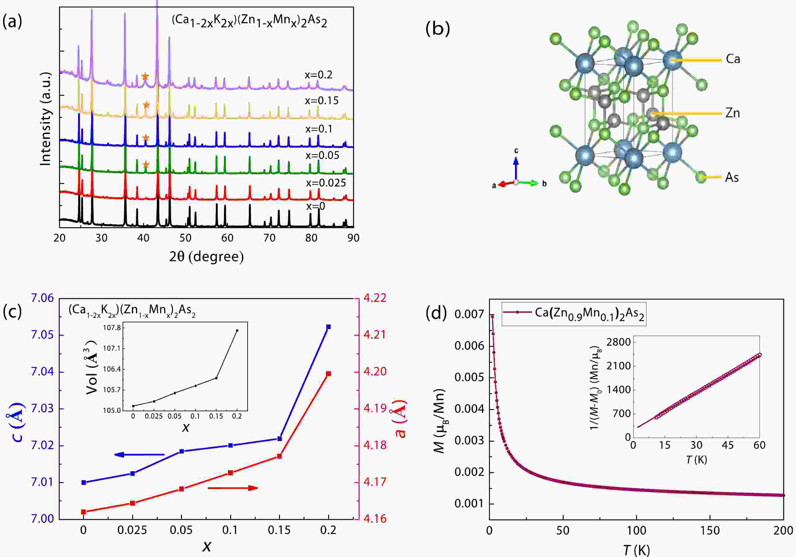
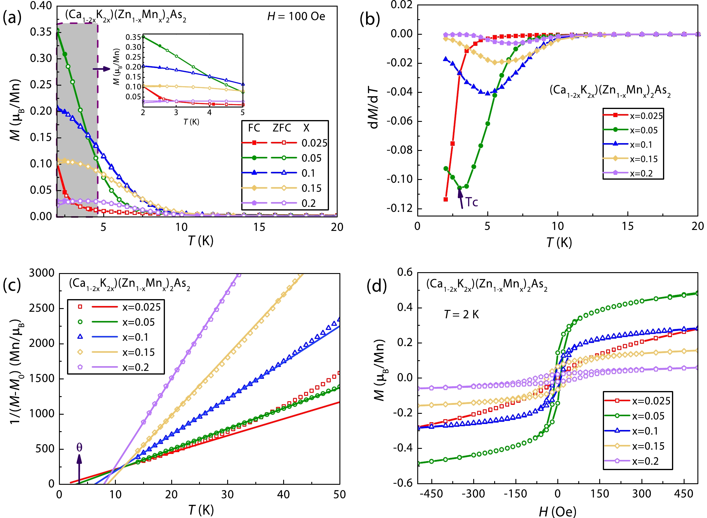
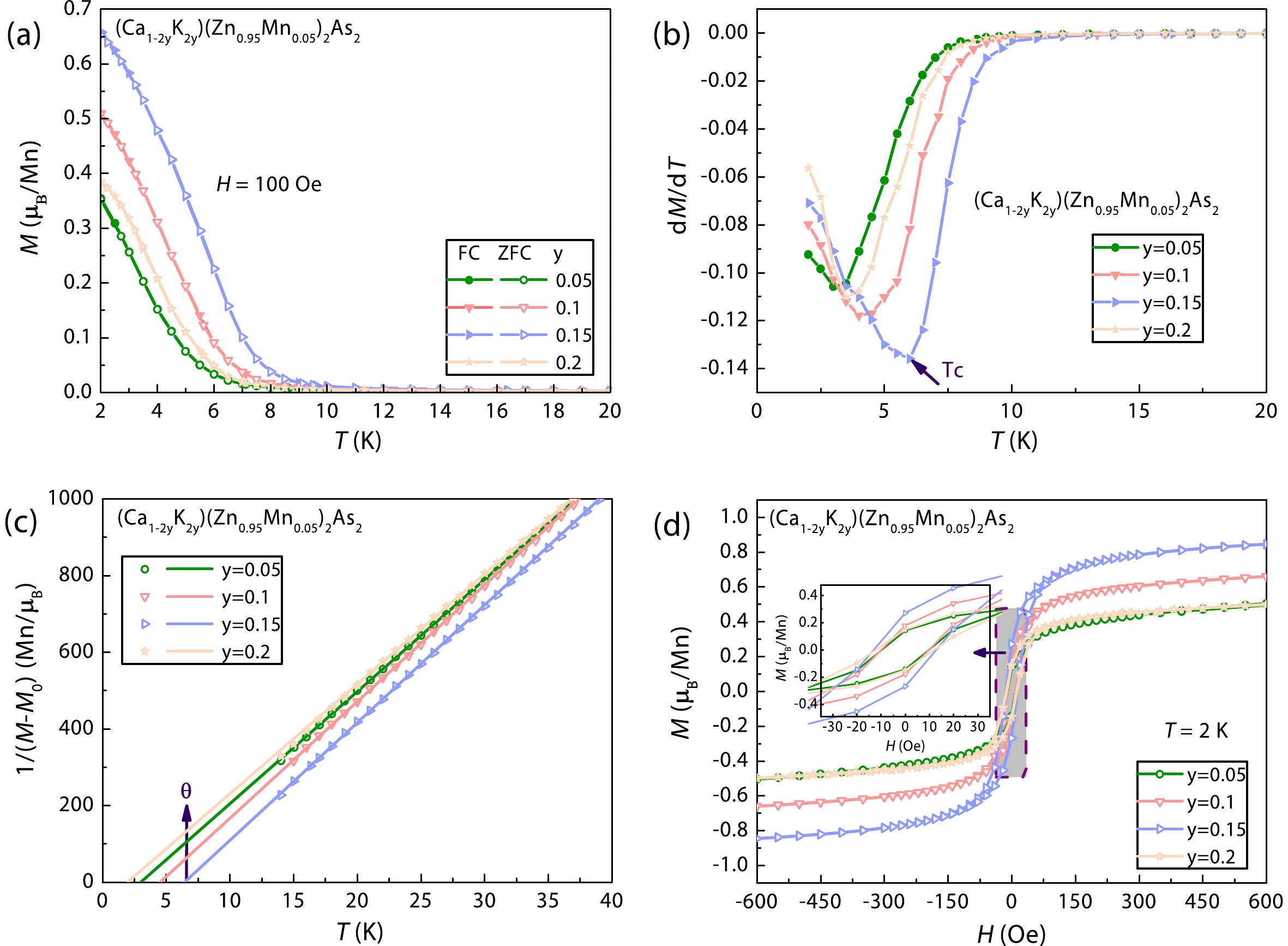
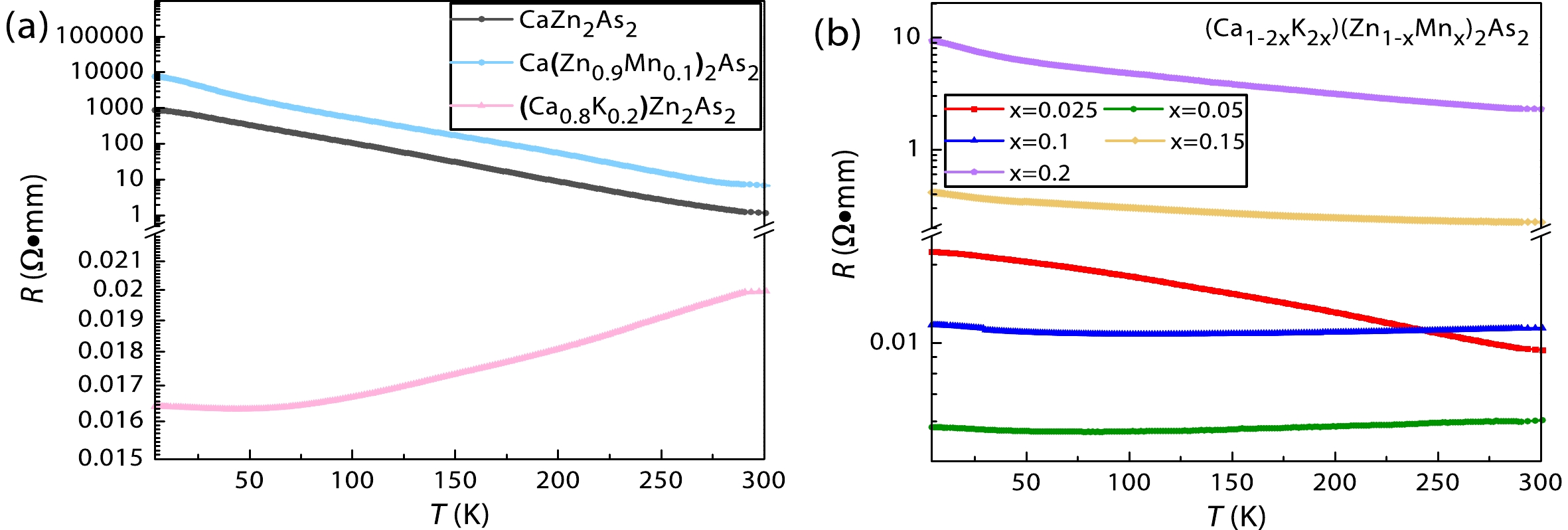
We have successfully synthesized a novel diluted magnetic semiconductor (Ca1−2xK2x)(Zn1−xMnx)2As2 with decoupled charge and spin doping. The substitutions of (Ca2+, K+) and (Zn2+, Mn2+) in the parent compound CaZn2As2 (space group P


J. Semicond.
2022, 43(7): 072801 doi: 10.1088/1674-4926/43/7/072801
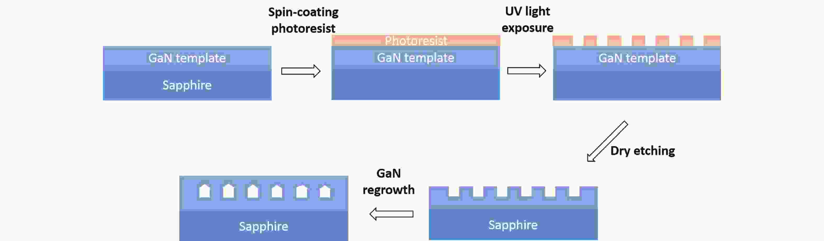
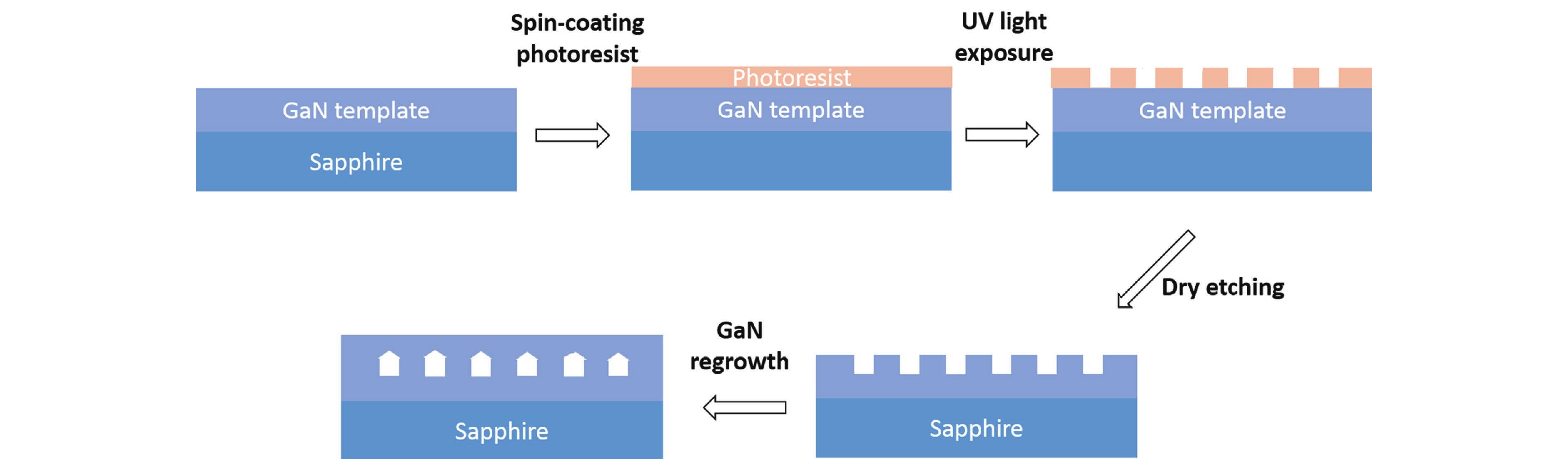
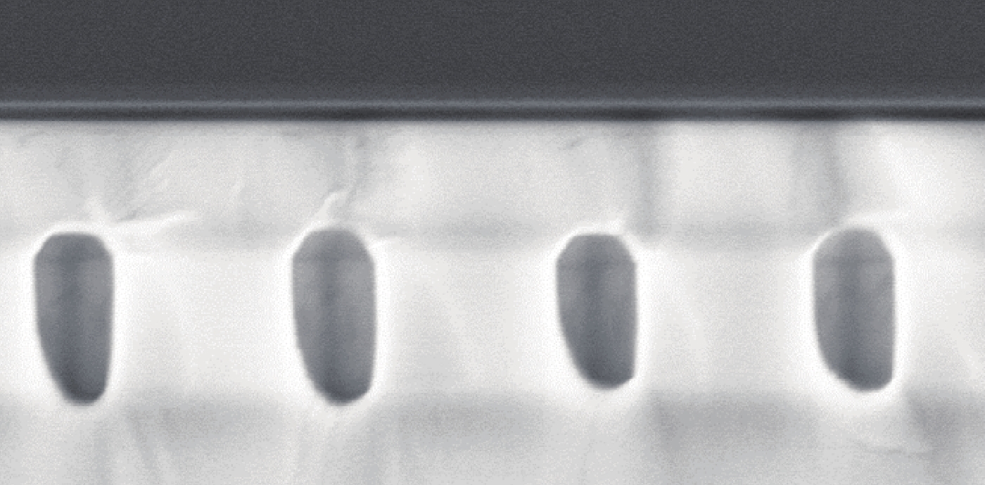
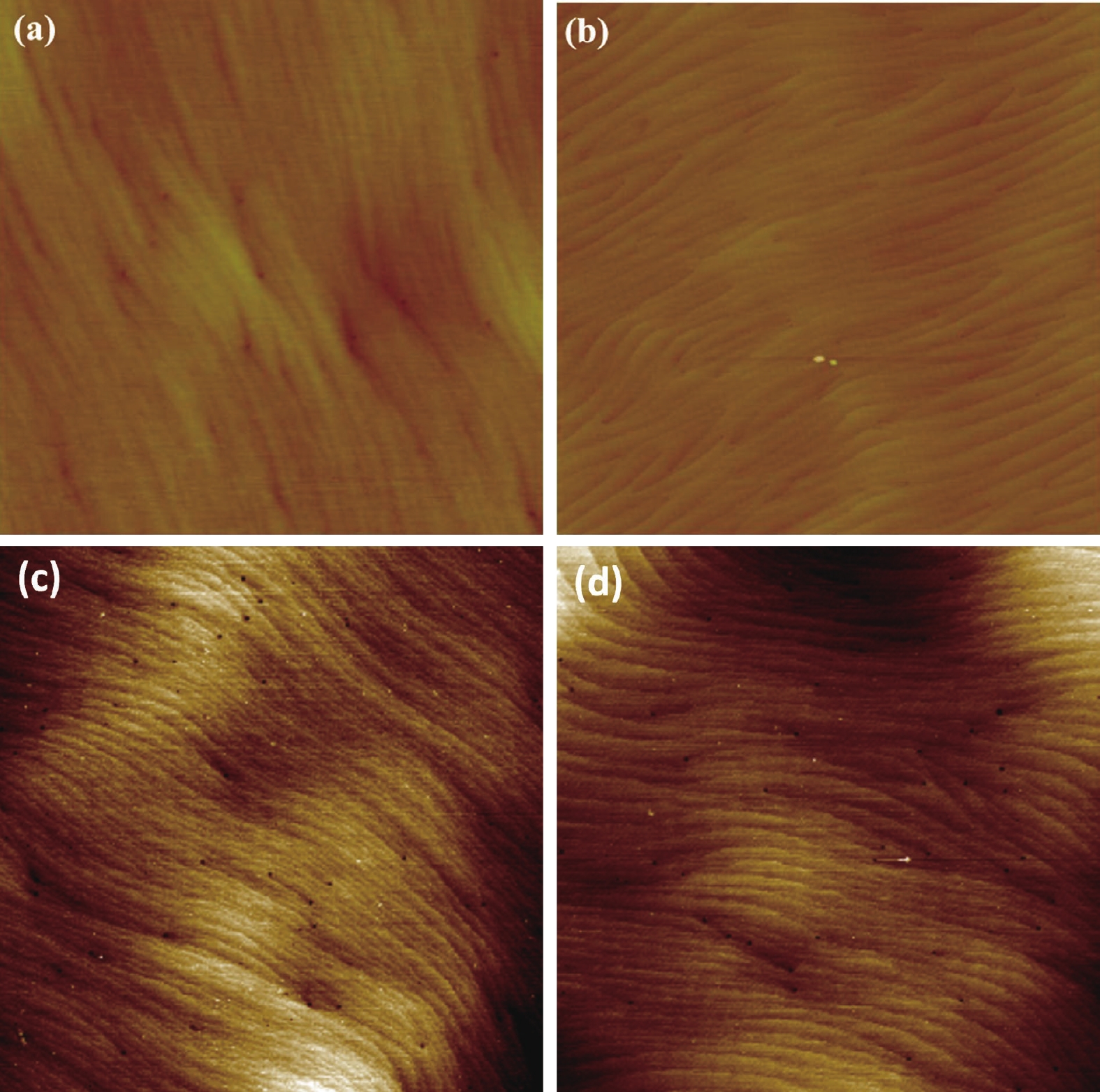
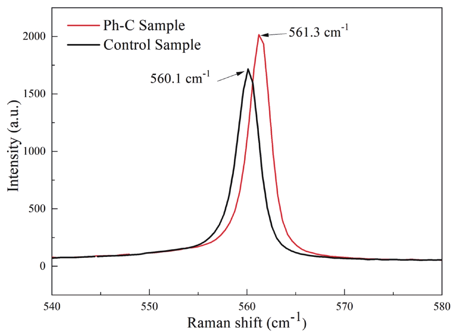
We report on the effect of inserted photonic crystalline (Ph-C) in the GaN epitaxial layer on the incorporation of the indium component for the InGaN-based green LED. The adoption of Ph-C in the GaN layer shifted the Raman peak value of E2 mode of GaN to lower frequency and resulted in a tensive stress relief. The stress relief can be attributed to strained lattices restoring in the matrix of Ph-C and the GaN pseudo-epitaxy over the air-void of the Ph-C. Moreover, the HRXRD rocking curves and AFM results show that the insertion of Ph-C also improves the crystal quality. With the inserted Ph-C, the indium component in the multiple quantum wells of the green LED (Ph-C LED) was enhanced. This resulted in a 6-nm red-shift of the peak wavelength. Furthermore, the LOP of the Ph-C LED was enhanced by 10.65% under an injection current of 20 mA.