Issue Browser
Volume 43, Issue 8,
Aug 2022
Column

J. Semicond.
2022, 43(8): 081001 doi: 10.1088/1674-4926/43/8/081001
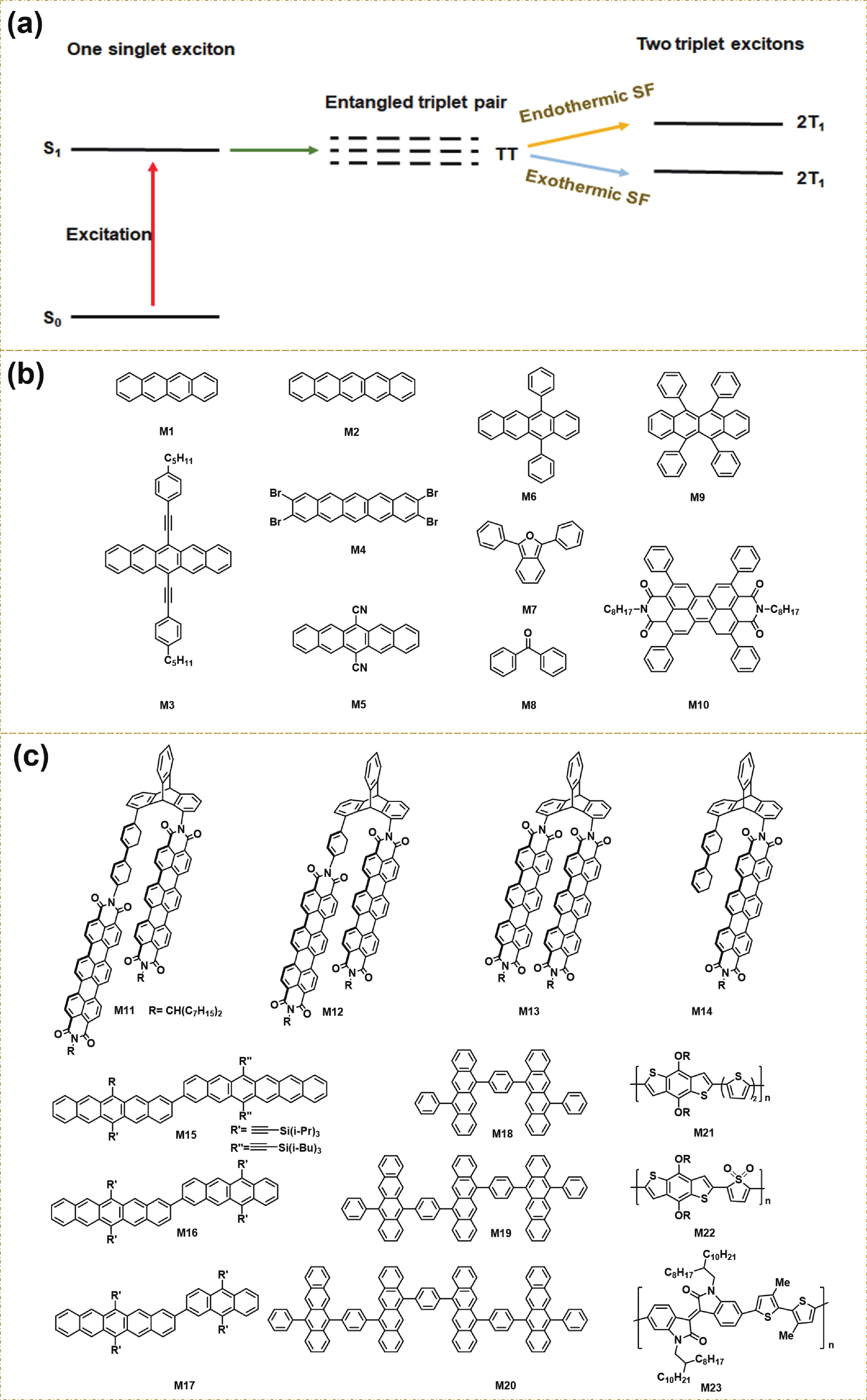
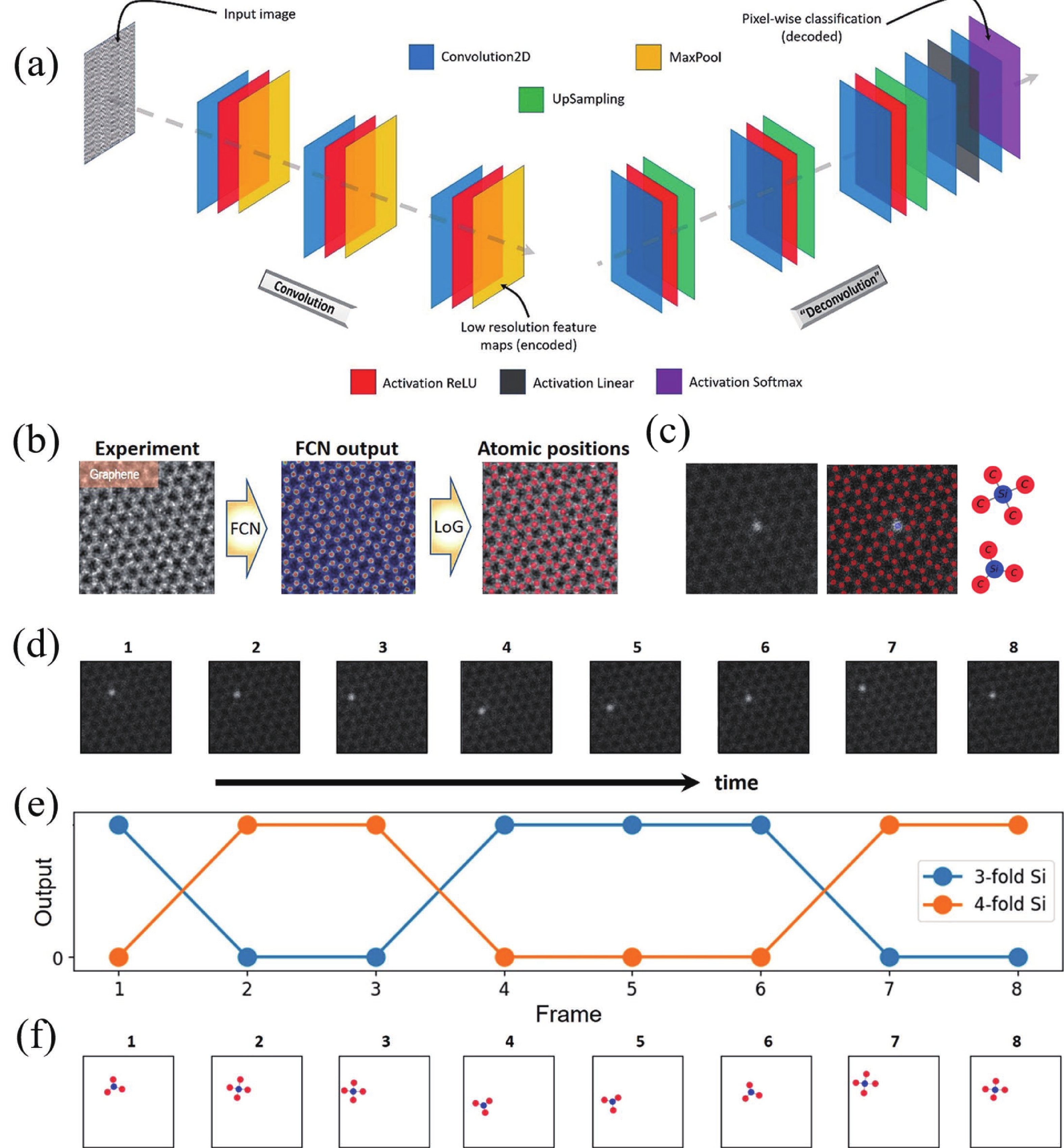
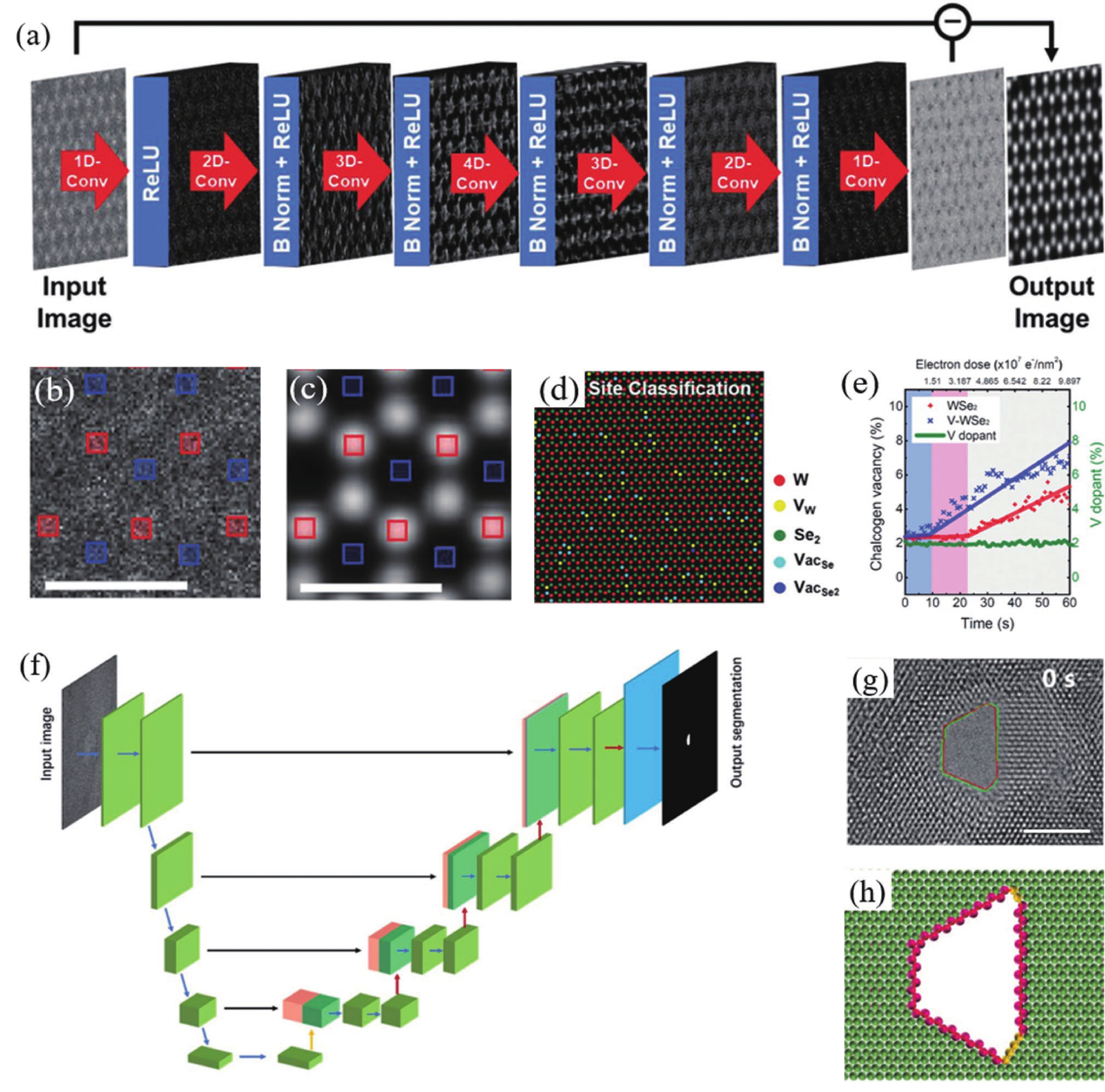
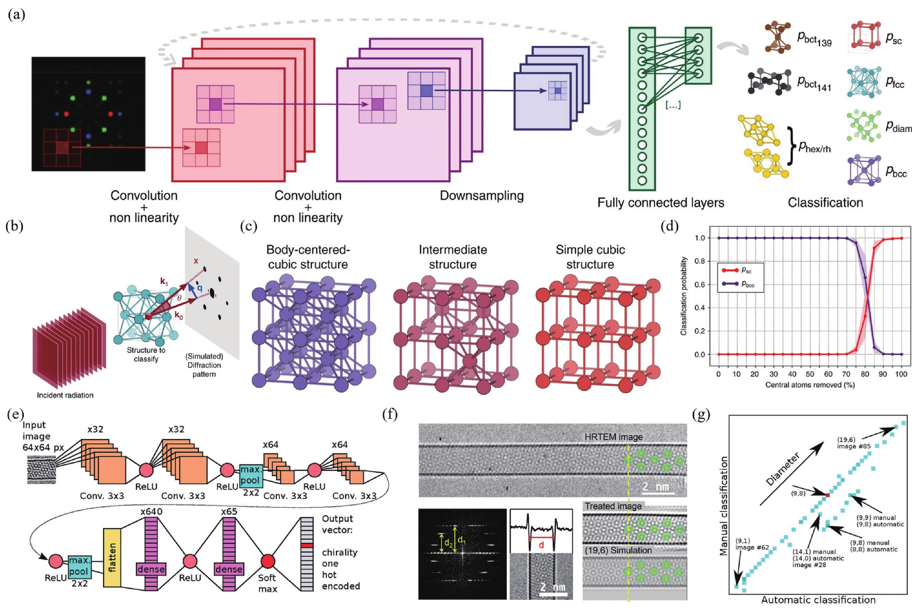
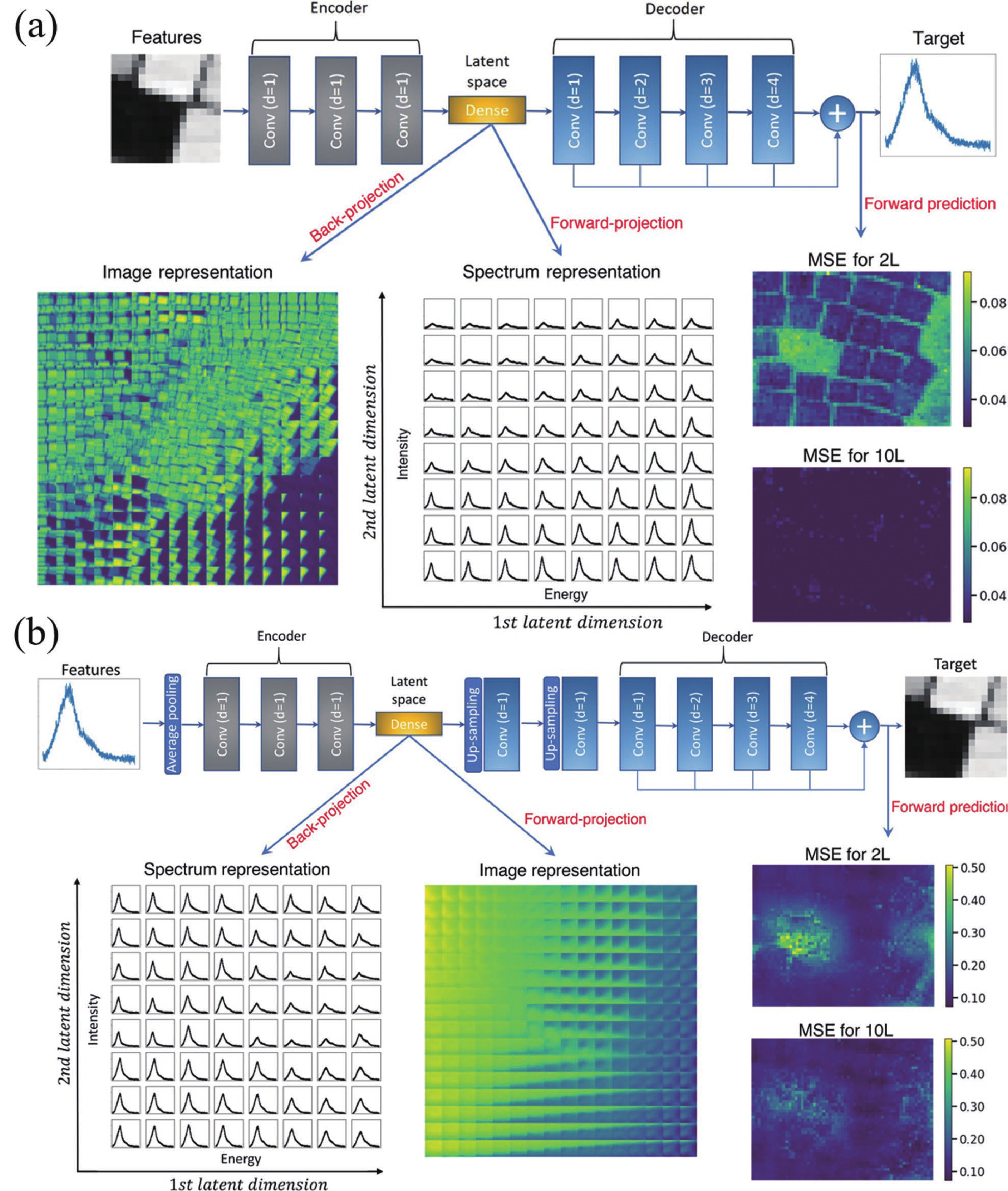
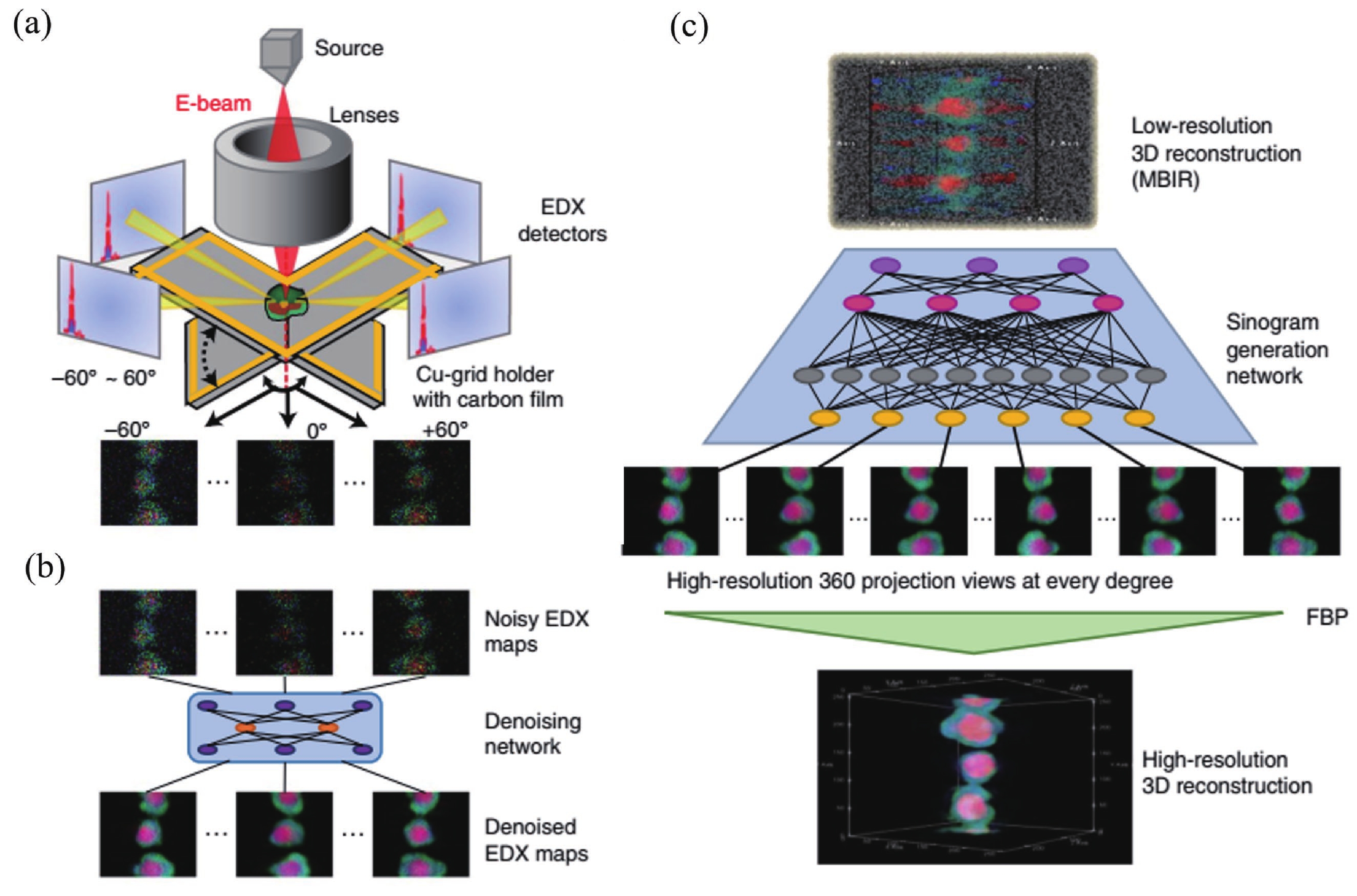
Advanced electronic materials are the fundamental building blocks of integrated circuits (ICs). The microscale properties of electronic materials (e.g., crystal structures, defects, and chemical properties) can have a considerable impact on the performance of ICs. Comprehensive characterization and analysis of the material in real time with high-spatial resolution are indispensable. In situ transmission electron microscope (TEM) with atomic resolution and external field can be applied as a physical simulation platform to study the evolution of electronic material in working conditions. The high-speed camera of the in situ TEM generates a high frame rate video, resulting in a large dataset that is beyond the data processing ability of researchers using the traditional method. To overcome this challenge, many works on automated TEM analysis by using machine-learning algorithm have been proposed. In this review, we introduce the technical evolution of TEM data acquisition, including analysis, and we summarize the application of machine learning to TEM data analysis in the aspects of morphology, defect, structure, and spectra. Some of the challenges of automated TEM analysis are given in the conclusion.

J. Semicond.
2022, 43(8): 081301 doi: 10.1088/1674-4926/43/8/081301
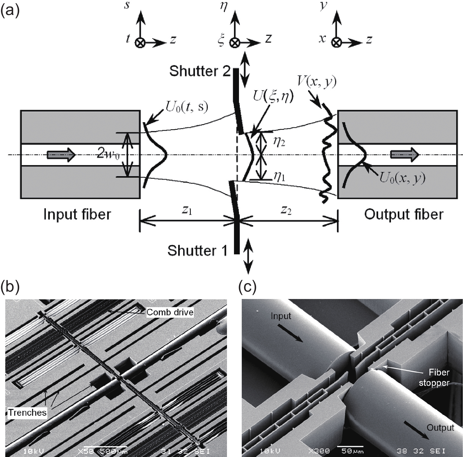
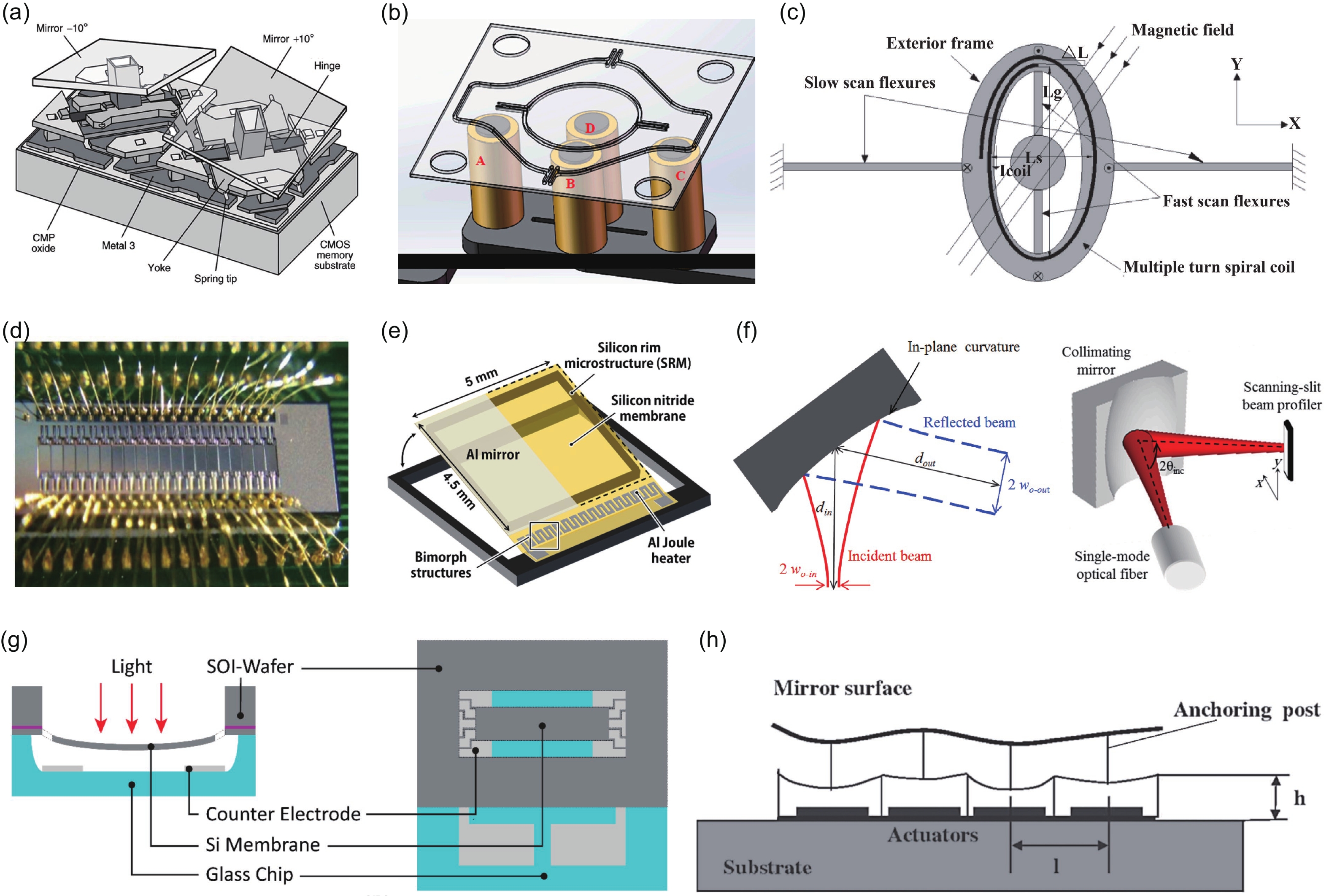
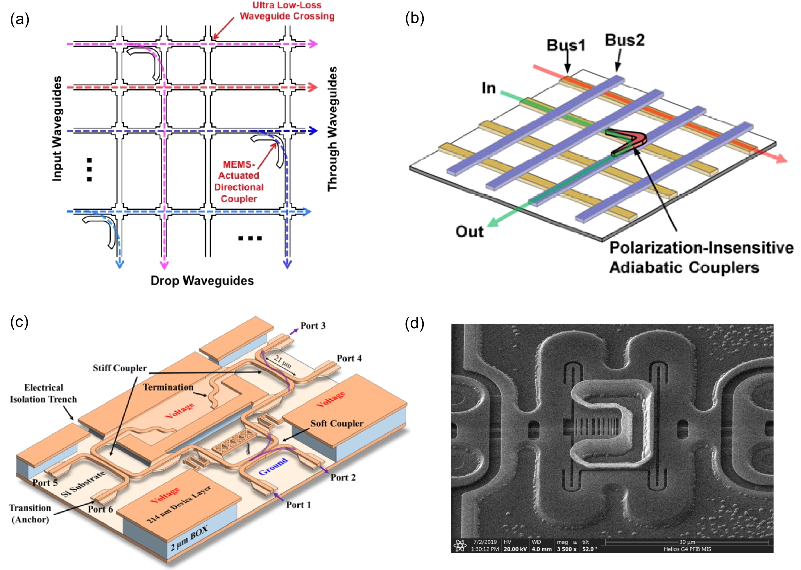
Micro-optical electromechanical systems (MOEMS) combine the merits of micro-electromechanical systems (MEMS) and micro-optics to enable unique optical functions for a wide range of advanced applications. Using simple external electromechanical control methods, such as electrostatic, magnetic or thermal effects, Si-based MOEMS can achieve precise dynamic optical modulation. In this paper, we will briefly review the technologies and applications of Si-based MOEMS. Their basic working principles, advantages, general materials and micromachining fabrication technologies are introduced concisely, followed by research progress of advanced Si-based MOEMS devices, including micromirrors/micromirror arrays, micro-spectrometers, and optical/photonic switches. Owing to the unique advantages of Si-based MOEMS in spatial light modulation and high-speed signal processing, they have several promising applications in optical communications, digital light processing, and optical sensing. Finally, future research and development prospects of Si-based MOEMS are discussed.

J. Semicond.
2022, 43(8): 082001 doi: 10.1088/1674-4926/43/8/082001
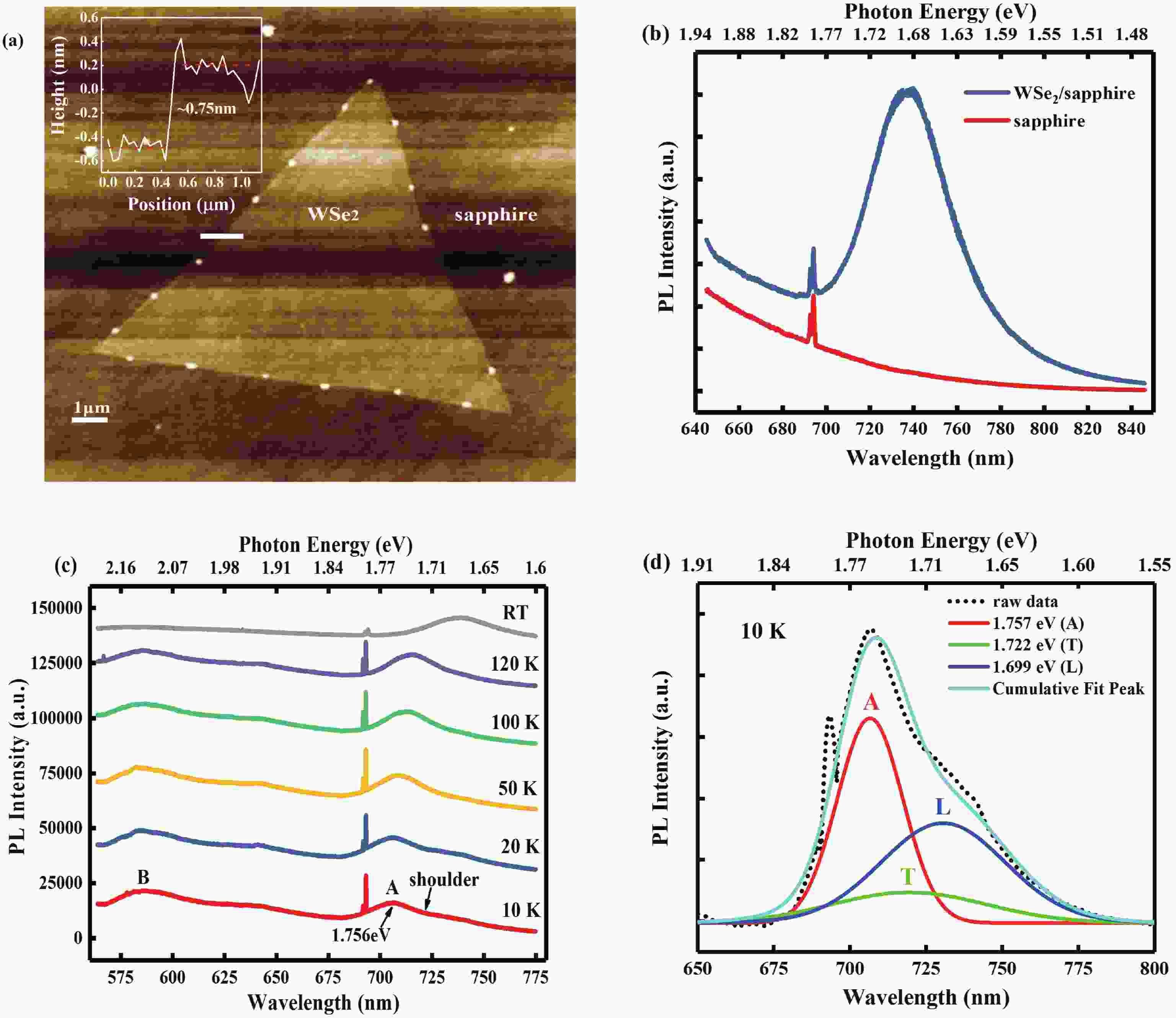
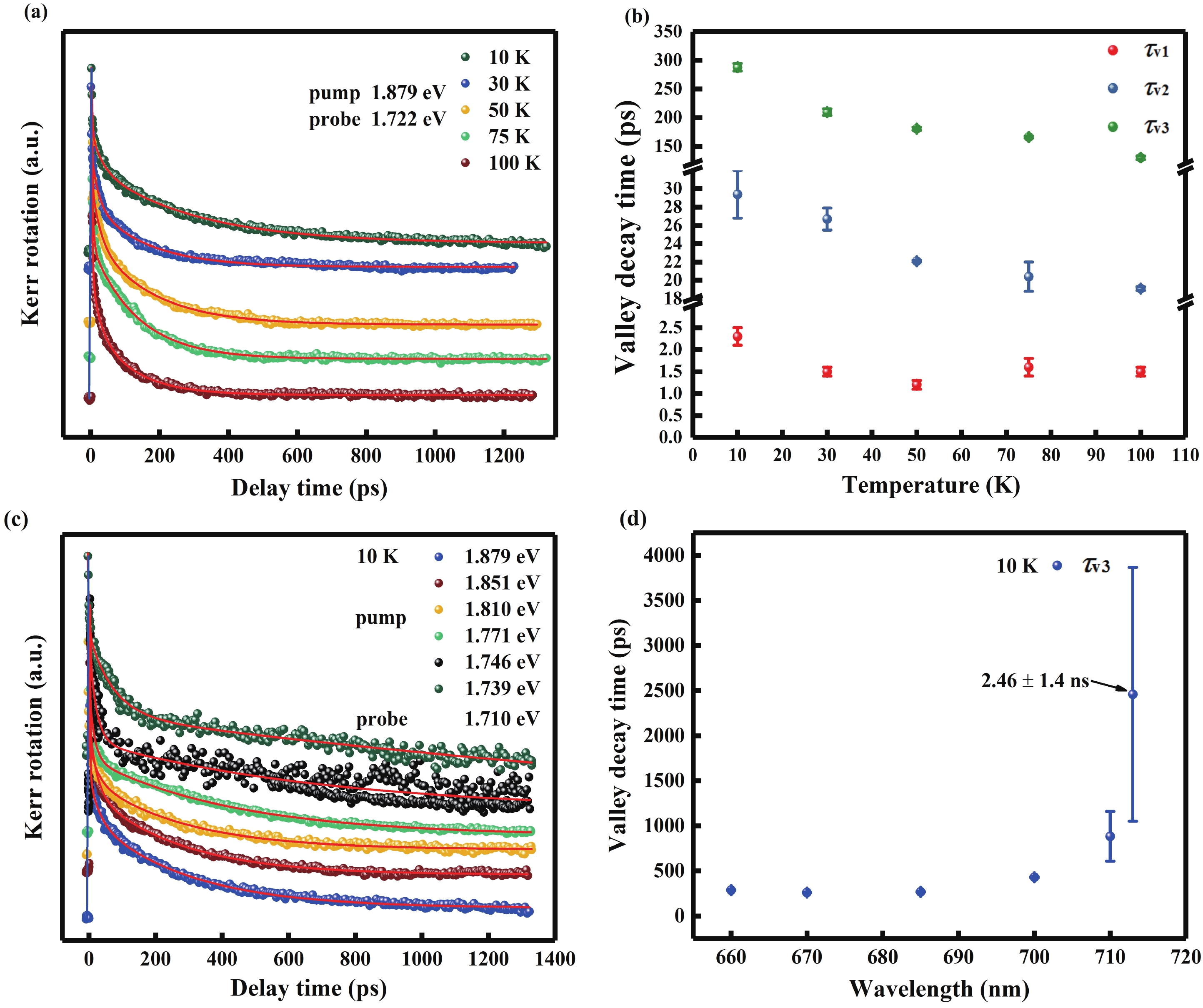
Monolayer transition-metal dichalcogenides possess rich excitonic physics and unique valley-contrasting optical selection rule, and offer a great platform for long spin/valley lifetime engineering and the associated spin/valleytronics exploration. Using two-color time-resolved Kerr rotation and time-resolved reflectivity spectroscopy, we investigate the spin/valley dynamics of different excitonic states in monolayer WSe2 grown by molecular beam epitaxy. With fine tuning of the photon energy of both pump and probe beams, the valley relaxation process for the neutral excitons and trions is found to be remarkably different—their characteristic spin/valley lifetimes vary from picoseconds to nanoseconds, respectively. The observed long trion spin lifetime of > 2.0 ns is discussed to be associated with the dark trion states, which is evidenced by the photon-energy dependent valley polarization relaxation. Our results also reveal that valley depolarization for these different excitonic states is intimately connected with the strong Coulomb interaction when the optical excitation energy is above the exciton resonance.


J. Semicond.
2022, 43(8): 082002 doi: 10.1088/1674-4926/43/8/082002
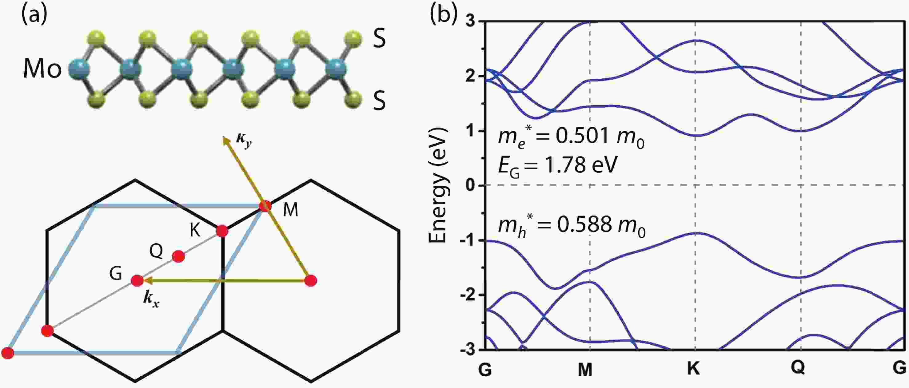
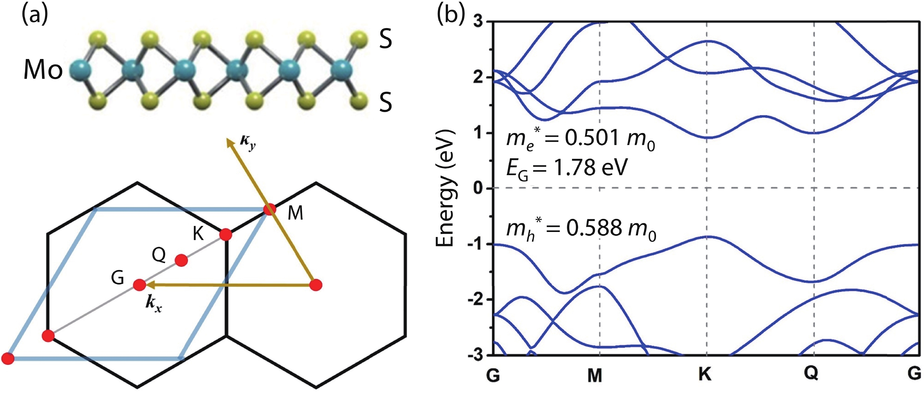
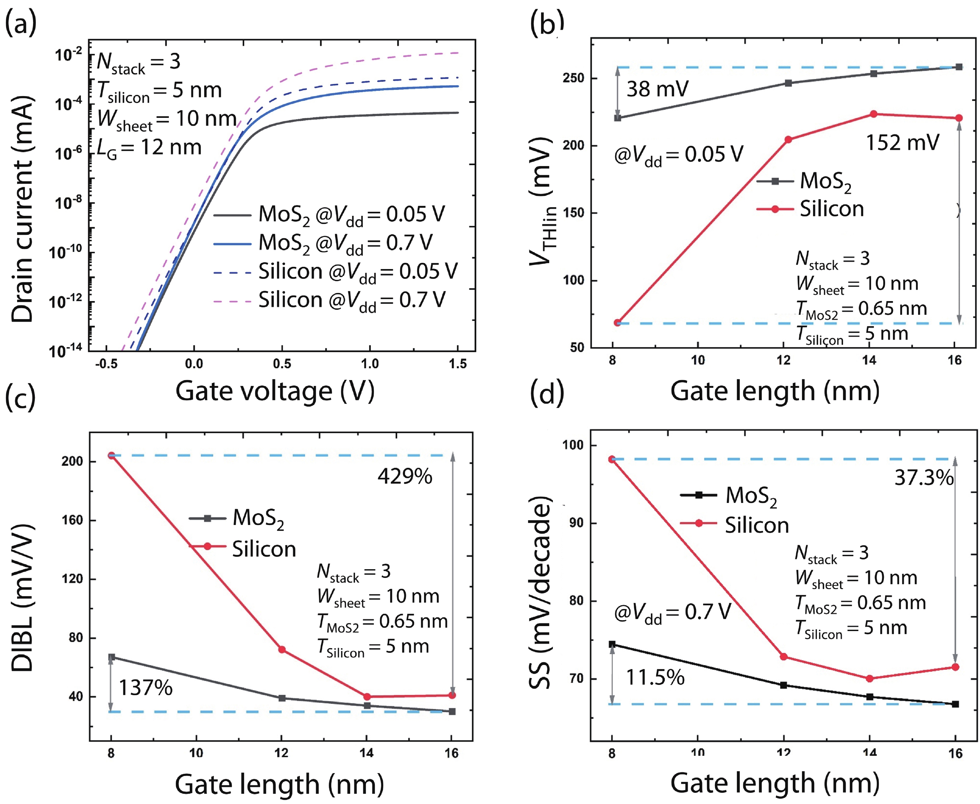
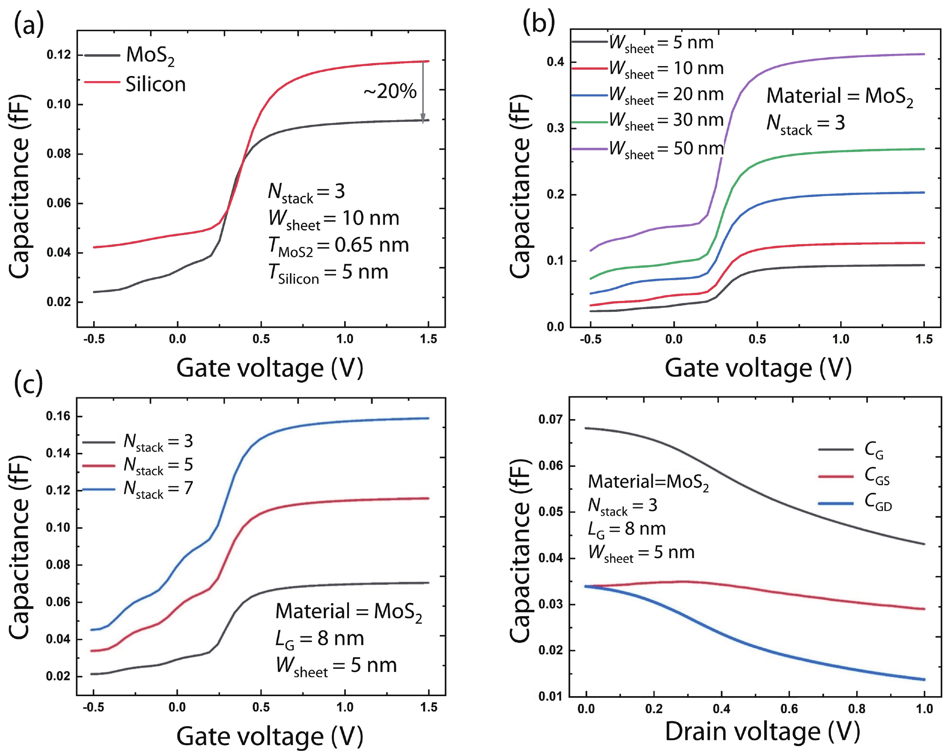
Transition metal dichalcogenides are nowadays appealing to researchers for their excellent electronic properties. Vertical stacked nanosheet FET (NSFET) based on MoS2 are proposed and studied by Poisson equation solver coupled with semi-classical quantum correction model implemented in Sentaurus workbench. It is found that, the 2D stacked NSFET can largely suppress short channel effects with improved subthreshold swing and drain induced barrier lowering, due to the excellent electrostatics of 2D MoS2. In addition, small-signal capacitance is extracted and analyzed. The MoS2 based NSFET shows great potential to enable next generation electronics.
J. Semicond.
2022, 43(8): 082301 doi: 10.1088/1674-4926/43/8/082301
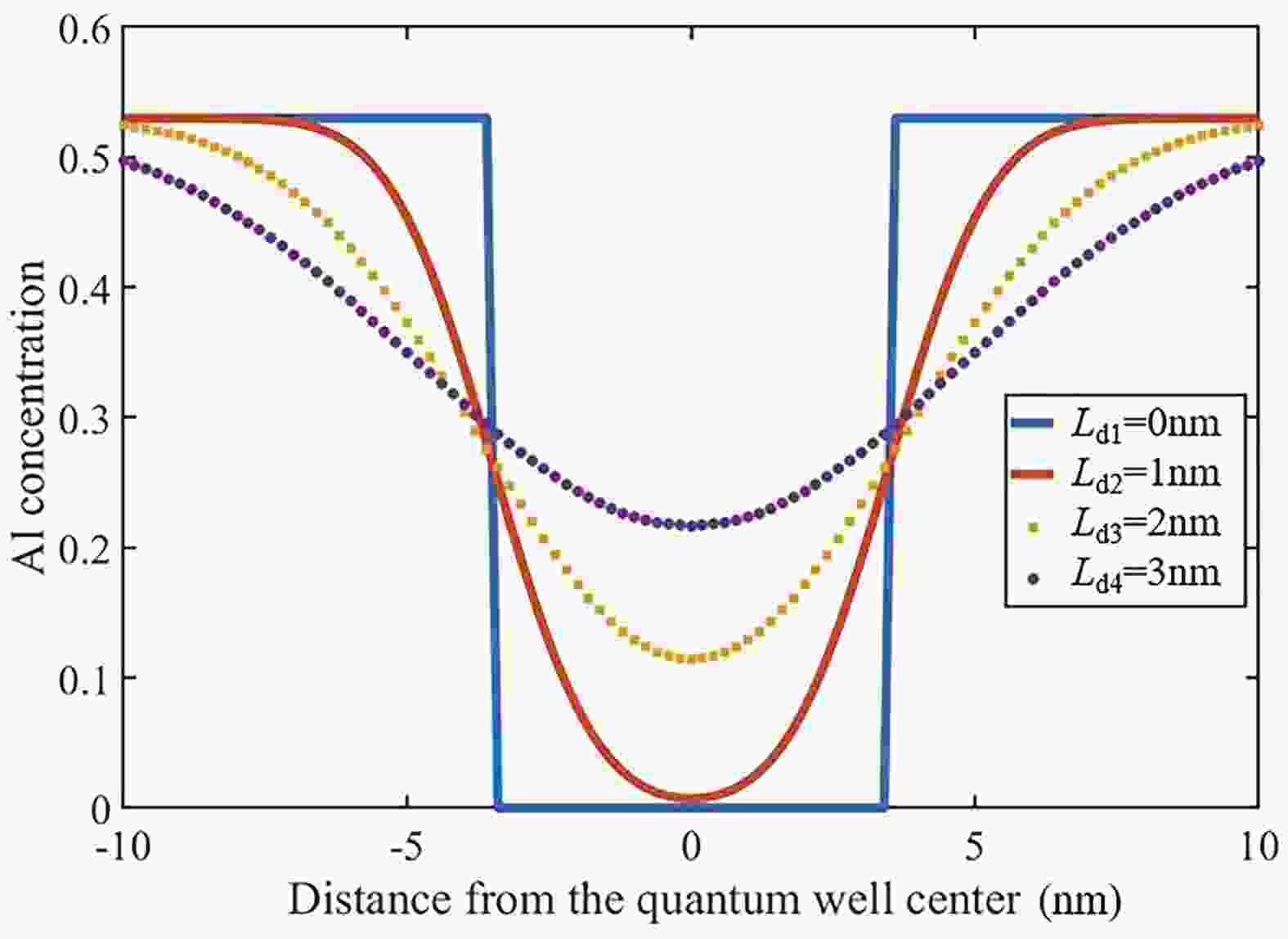
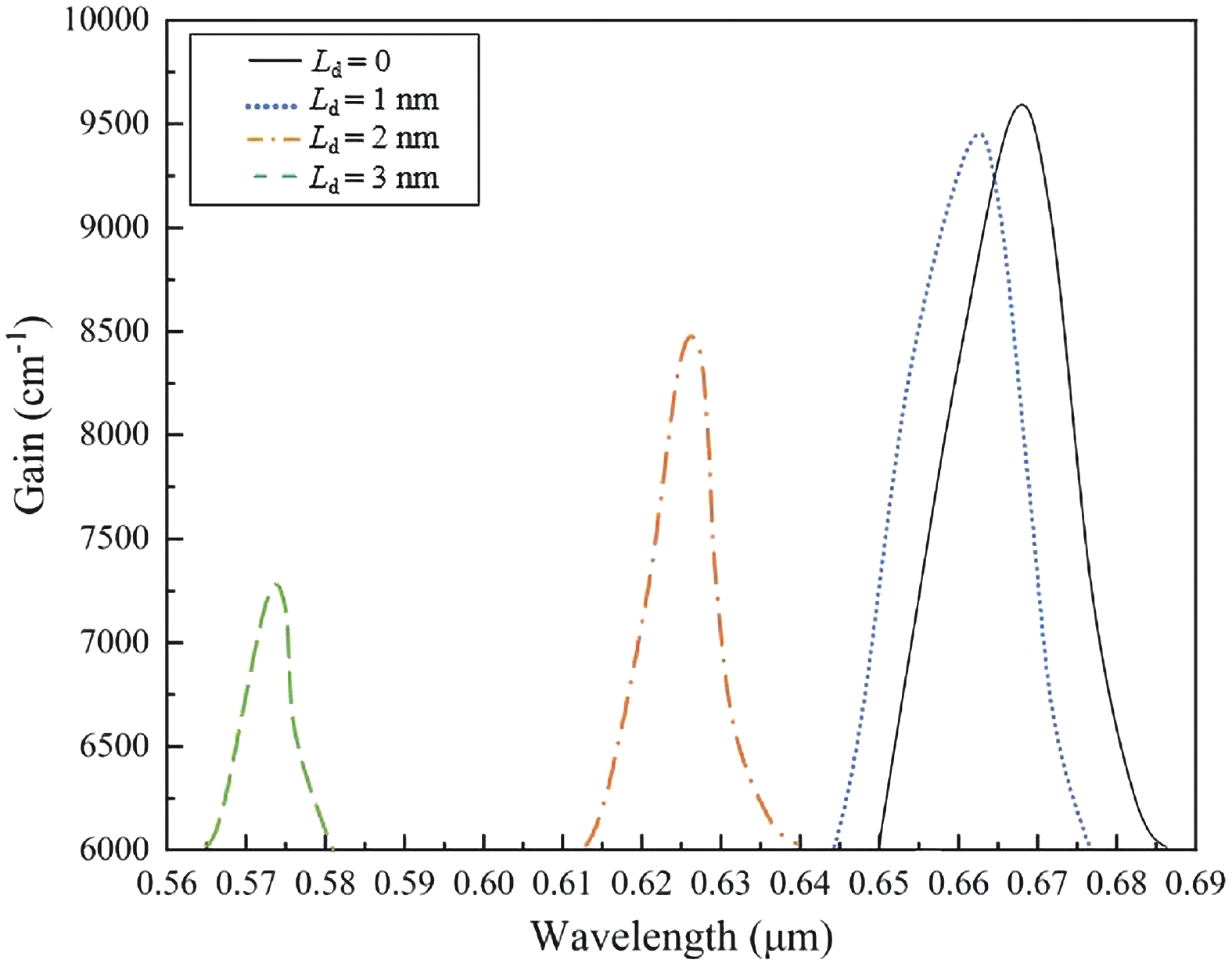
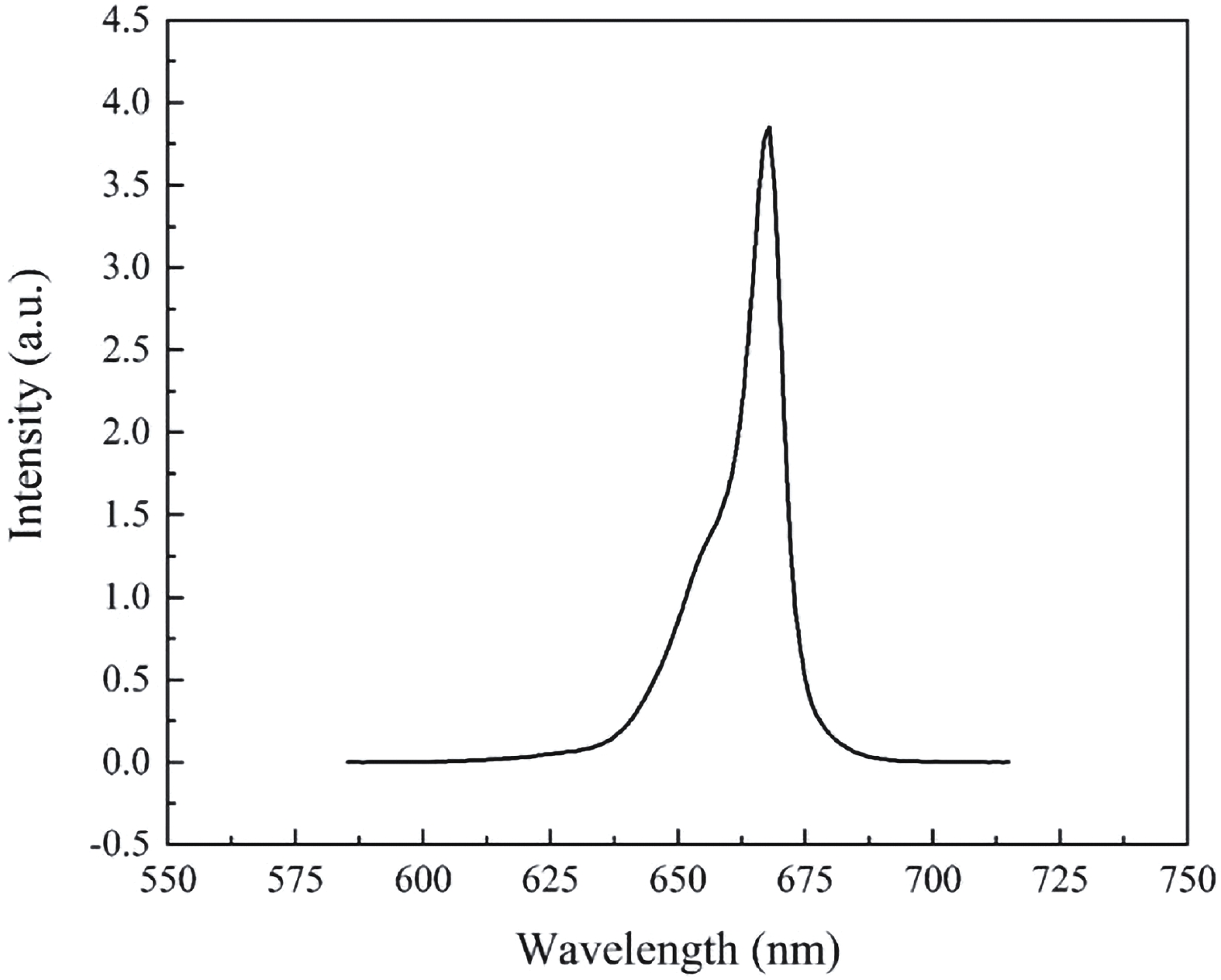
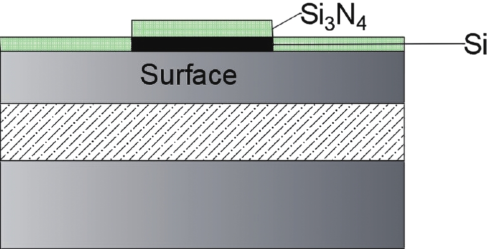
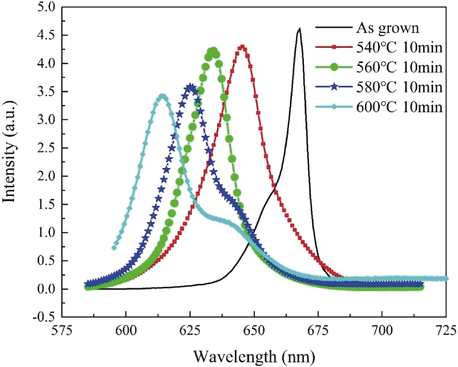
The optical catastrophic damage that usually occurs at the cavity surface of semiconductor lasers has become the main bottleneck affecting the improvement of laser output power and long-term reliability. To improve the output power of 680 nm AlGaInP/GaInP quantum well red semiconductor lasers, Si–Si3N4 composited dielectric layers are used to induce its quantum wells to be intermixed at the cavity surface to make a non-absorption window. Si with a thickness of 100 nm and Si3N4 with a thickness of 100 nm were grown on the surface of the epitaxial wafer by magnetron sputtering and PECVD as diffusion source and driving source, respectively. Compared with traditional Si impurity induced quantum well intermixing, this paper realizes the blue shift of 54.8 nm in the nonabsorbent window region at a lower annealing temperature of 600 °C and annealing time of 10 min. Under this annealing condition, the wavelength of the gain luminescence region basically does not shift to short wavelength, and the surface morphology of the whole epitaxial wafer remains fine after annealing. The application of this process condition can reduce the difficulty of production and save cost, which provides an effective method for upcoming fabrication.


J. Semicond.
2022, 43(8): 082401 doi: 10.1088/1674-4926/43/8/082401
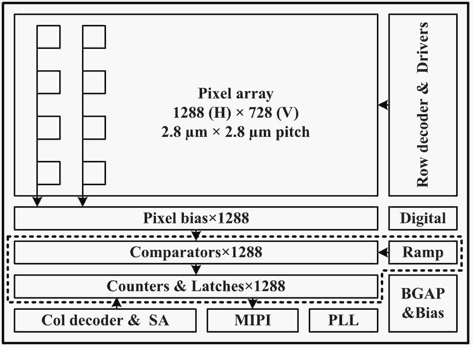
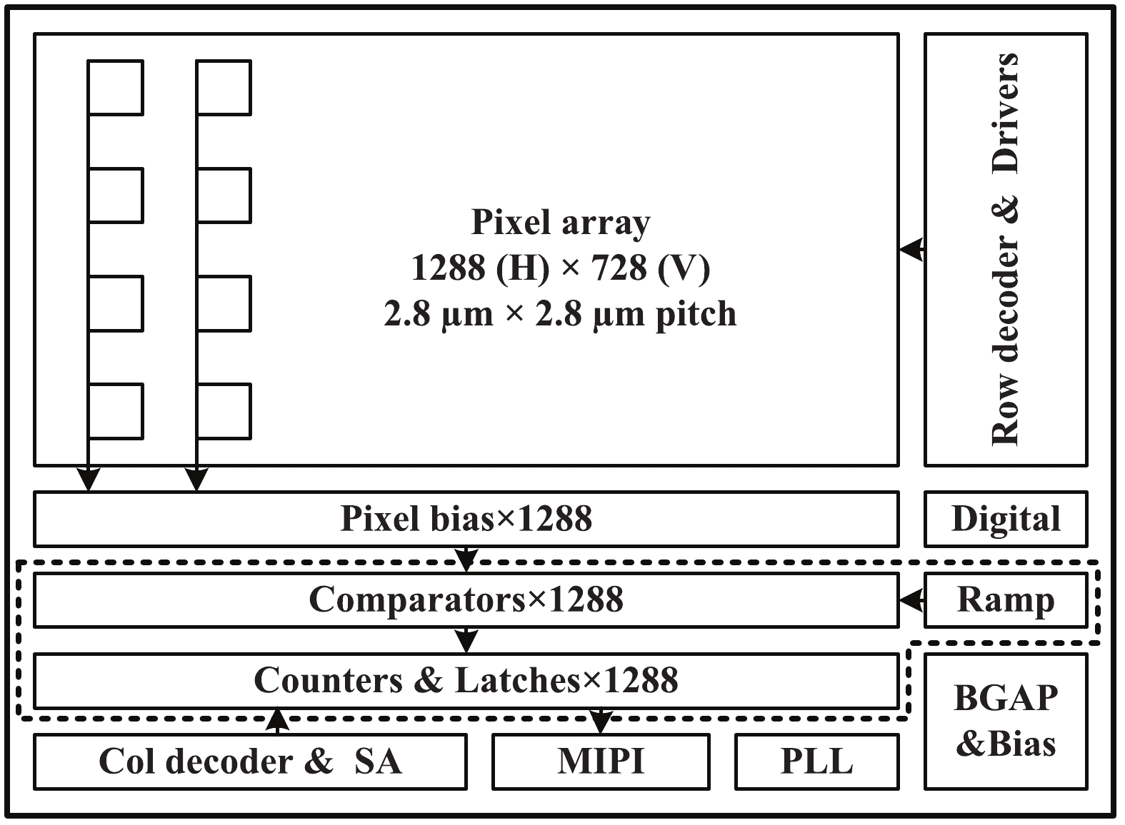
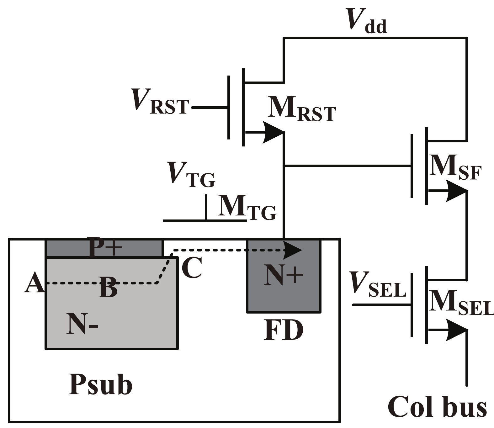
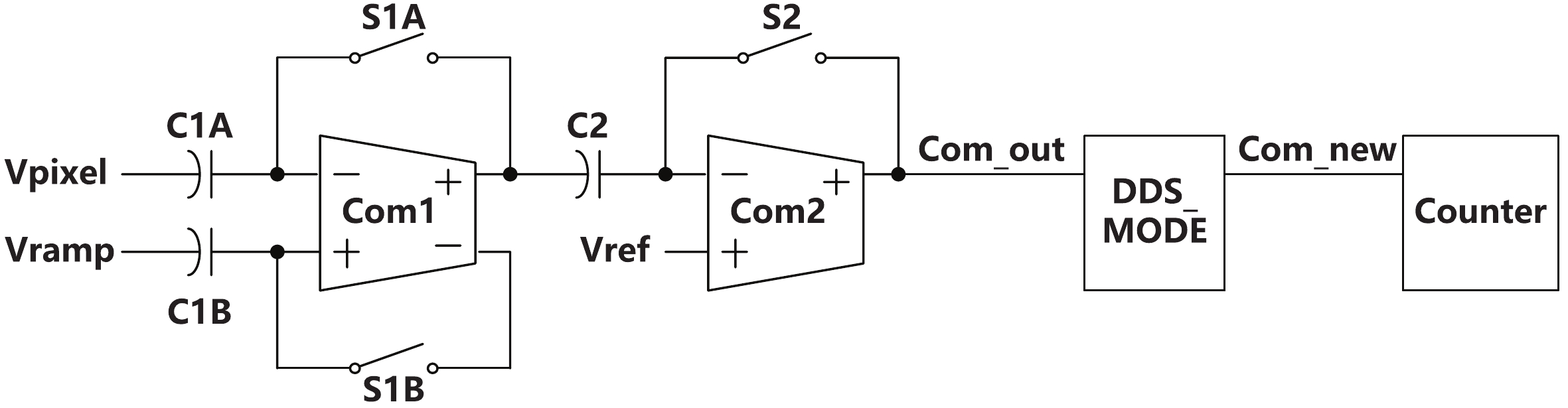
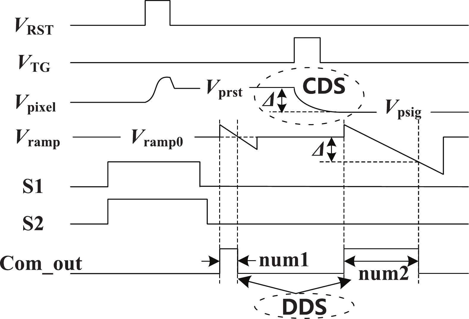
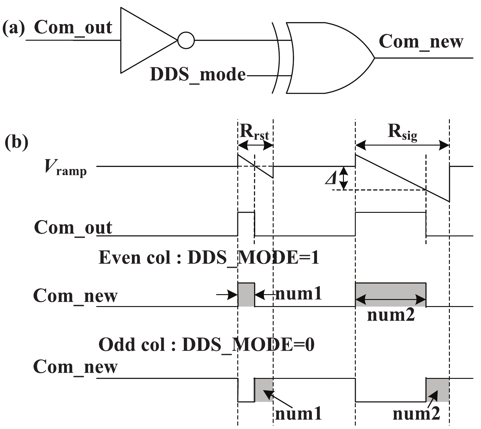
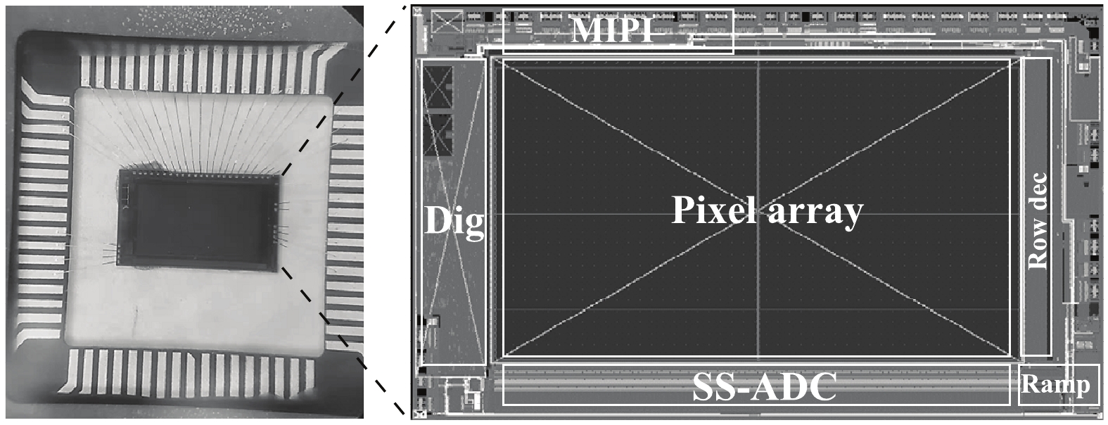
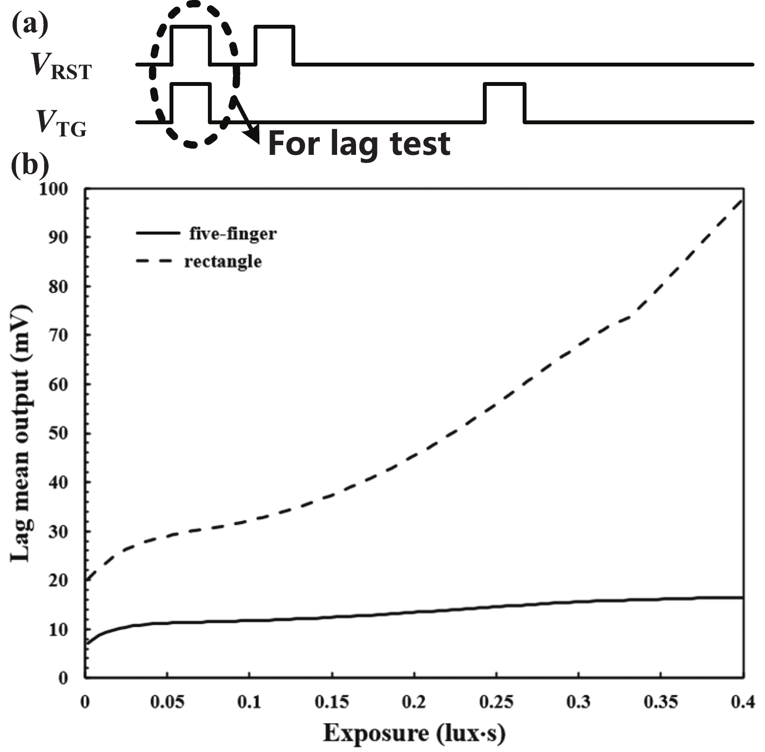
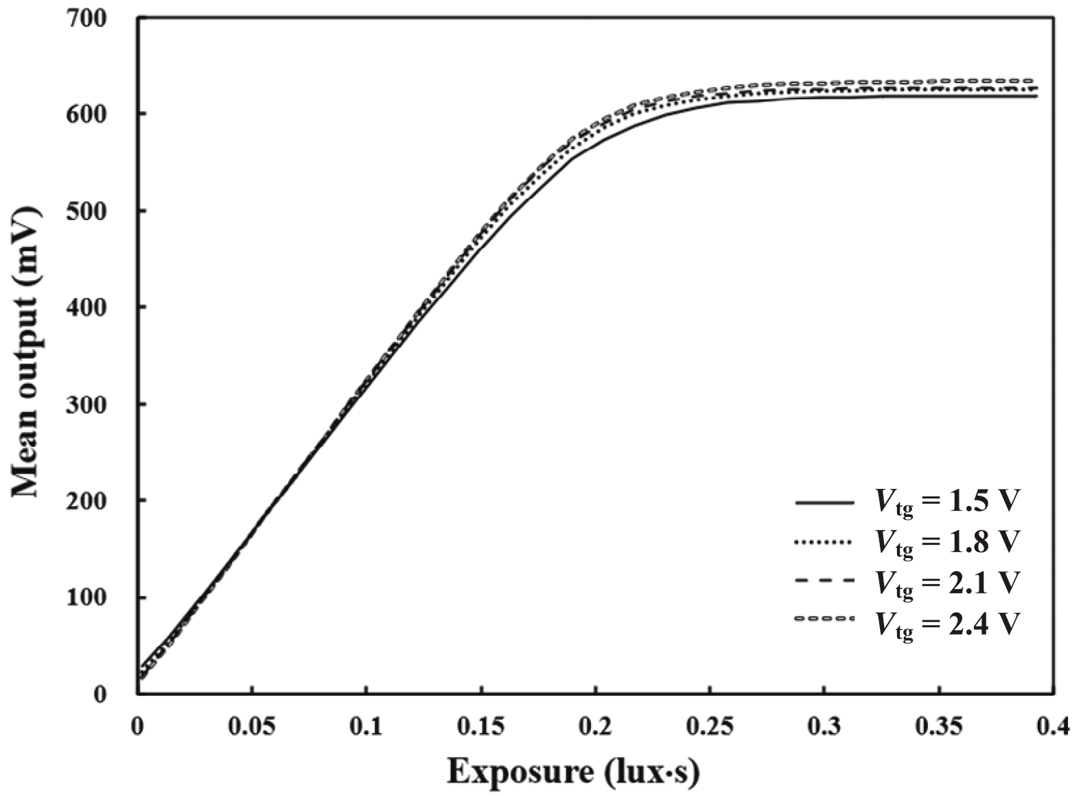
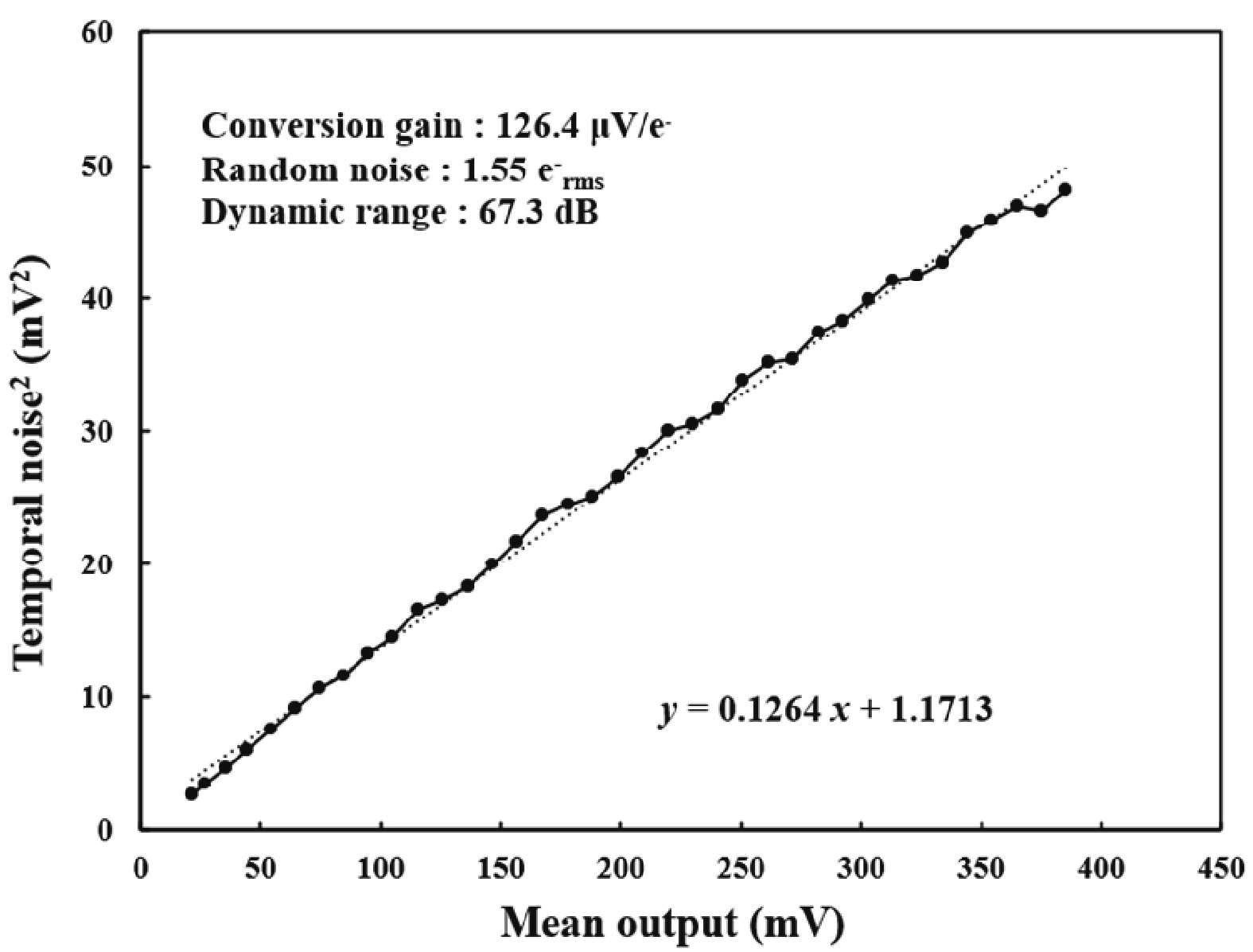
This paper presents a low-power high-quality CMOS image sensor (CIS) using 1.5 V 4T pinned photodiode (4T-PPD) and dual correlated double sampling (dual-CDS) column-parallel single-slope ADC. A five-finger shaped pixel layer is proposed to solve image lag caused by low-voltage 4T-PPD. Dual-CDS is used to reduce random noise and the nonuniformity between columns. Dual-mode counting method is proposed to improve circuit robustness. A prototype sensor was fabricated using a 0.11 µm CMOS process. Measurement results show that the lag of the five-finger shaped pixel is reduced by 80% compared with the conventional rectangular pixel, the chip power consumption is only 36 mW, the dynamic range is 67.3 dB, the random noise is only 1.55 e–rms, and the figure-of-merit is only 1.98 e–·nJ, thus realizing low-power and high-quality imaging.


J. Semicond.
2022, 43(8): 082601 doi: 10.1088/1674-4926/43/8/082601
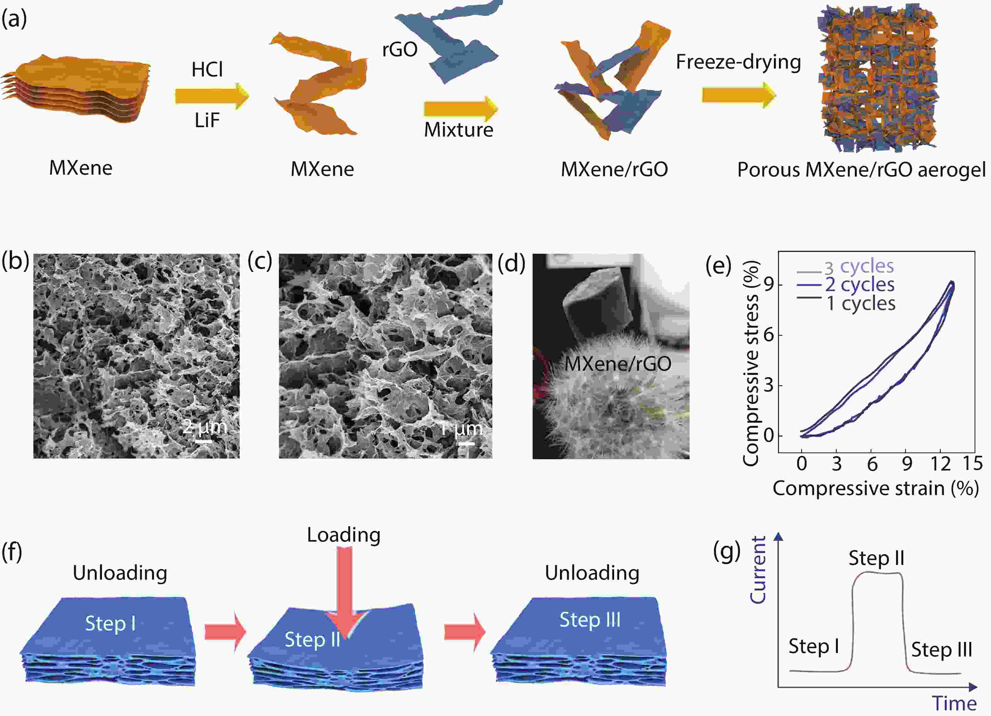
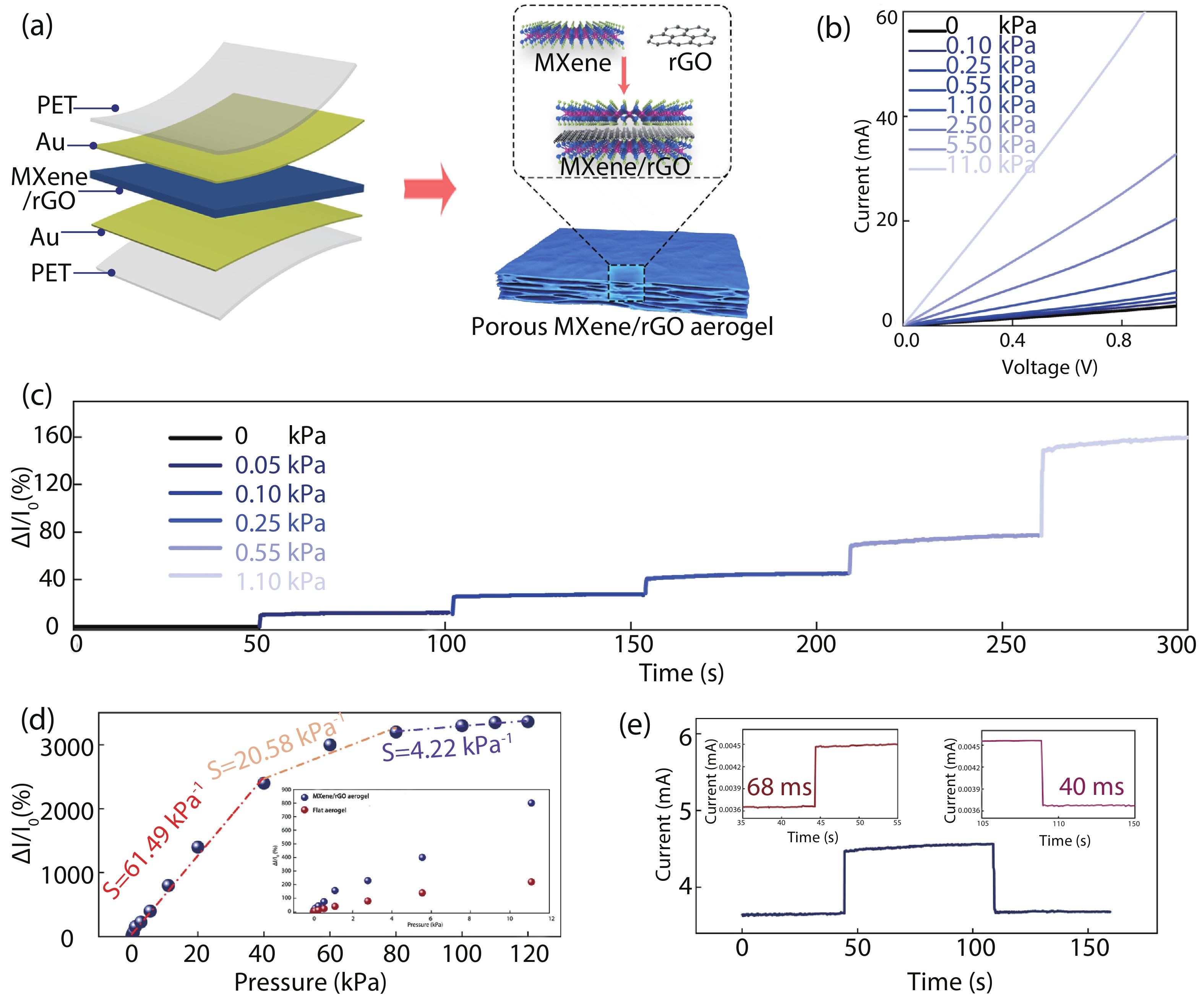
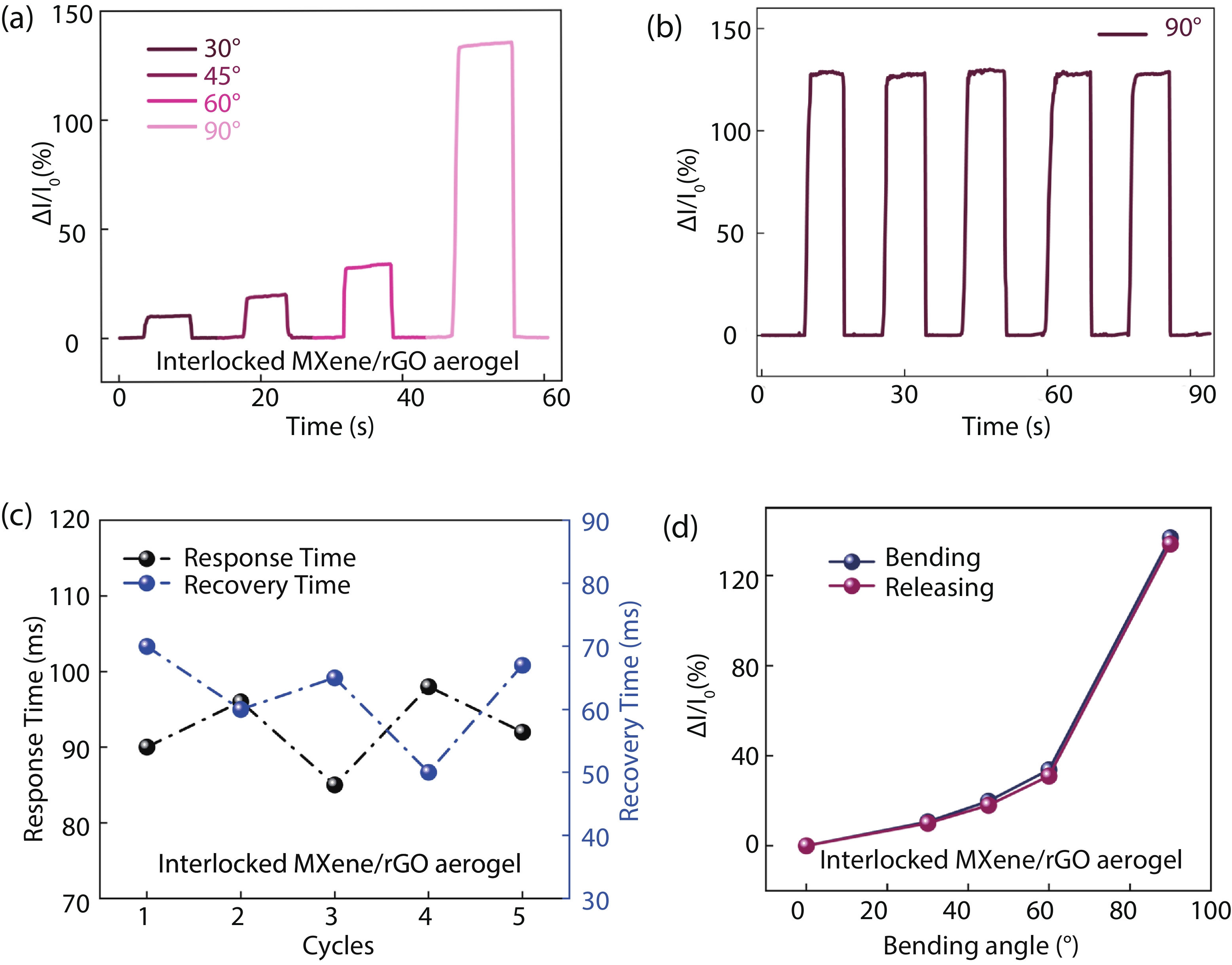
Two-dimensional (2D) materials have attracted considerable interest thanks to their unique electronic/physical–chemical characteristics and their potential for use in a large variety of sensing applications. However, few-layered nanosheets tend to agglomerate owing to van der Waals forces, which obstruct internal nanoscale transport channels, resulting in low electrochemical activity and restricting their use for sensing purposes. Here, a hybrid MXene/rGO aerogel with a three-dimensional (3D) interlocked network was fabricated via a freeze-drying method. The porous MXene/rGO aerogel has a lightweight and hierarchical porous architecture, which can be compressed and expanded several times without breaking. Additionally, a flexible pressure sensor that uses the aerogel as the sensitive layer has a wide response range of approximately 0–40 kPa and a considerable response within this range, averaging approximately 61.49 kPa–1. The excellent sensing performance endows it with a broad range of applications, including human-computer interfaces and human health monitoring.


J. Semicond.
2022, 43(8): 082801 doi: 10.1088/1674-4926/43/8/082801
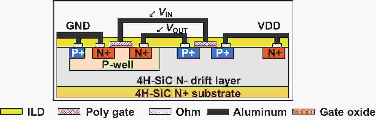
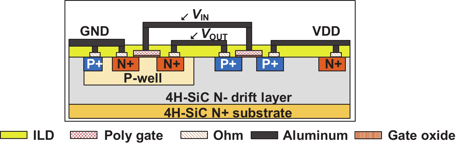
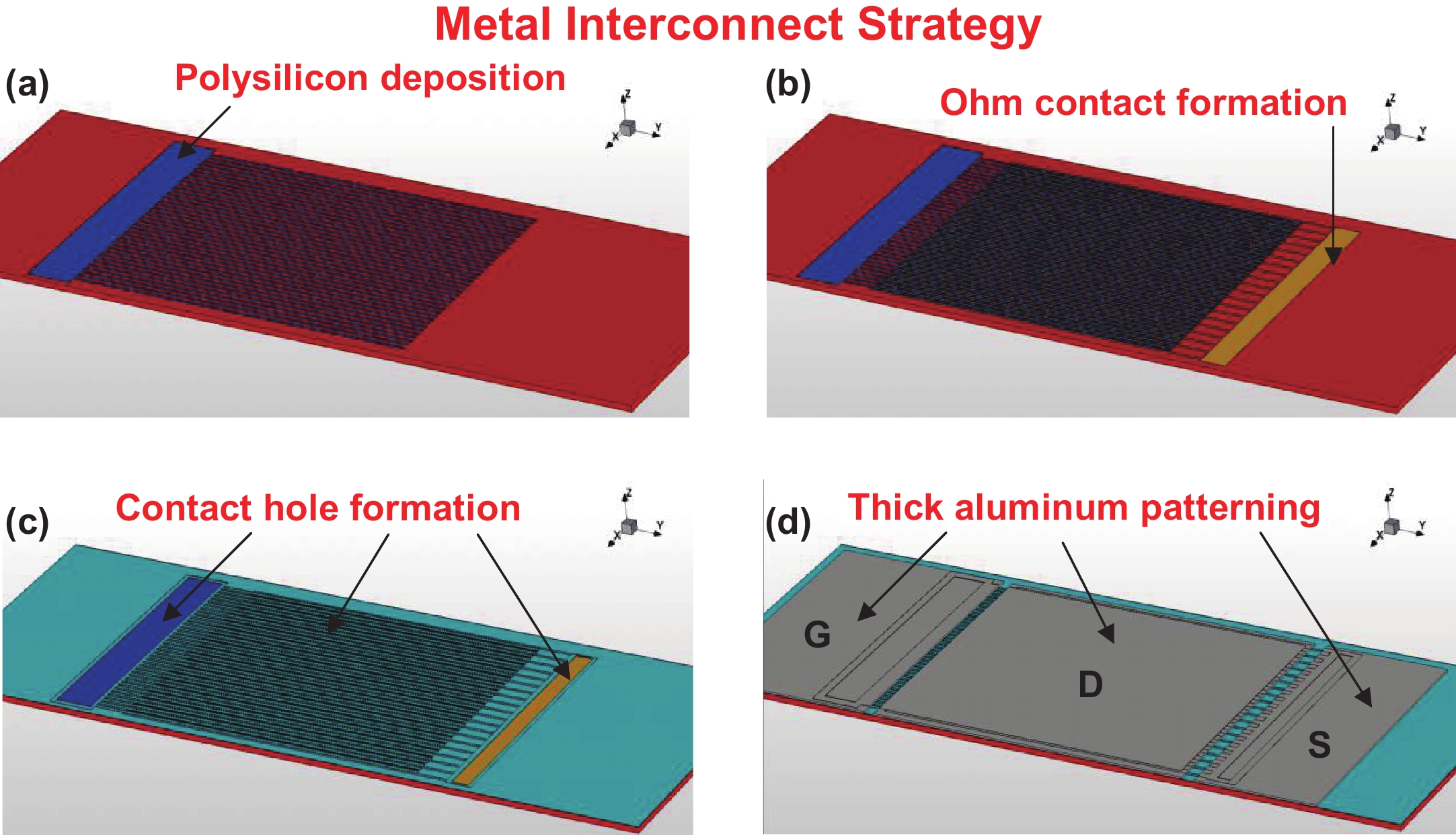
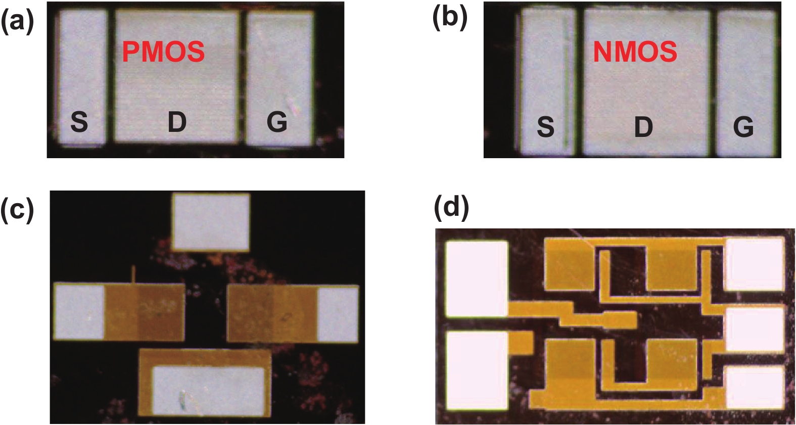
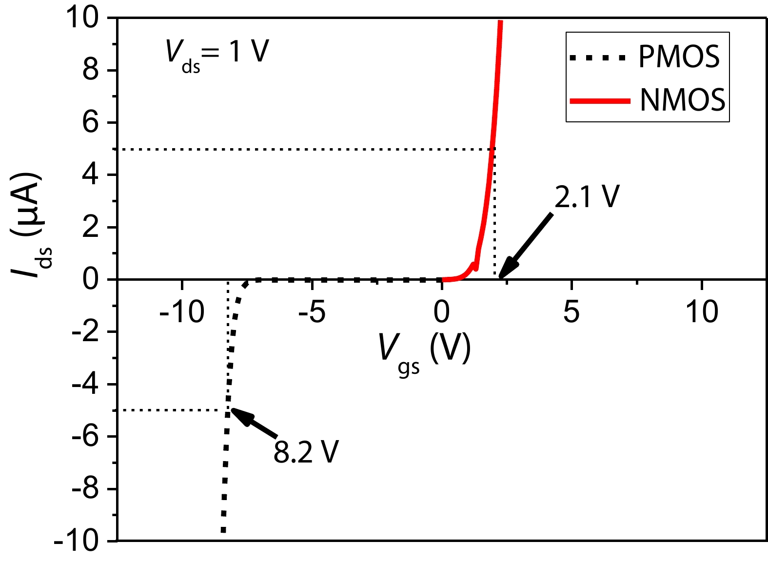
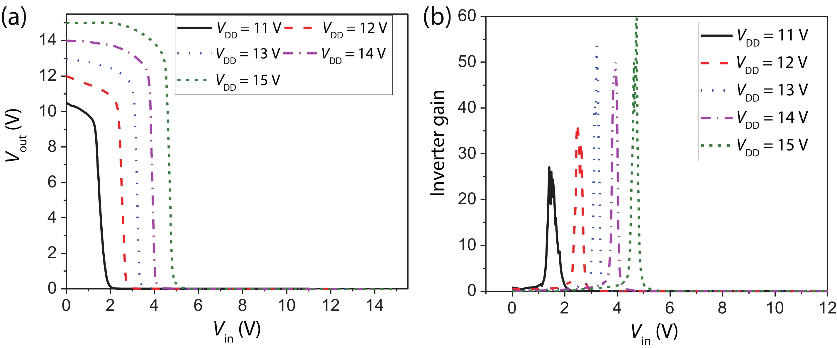
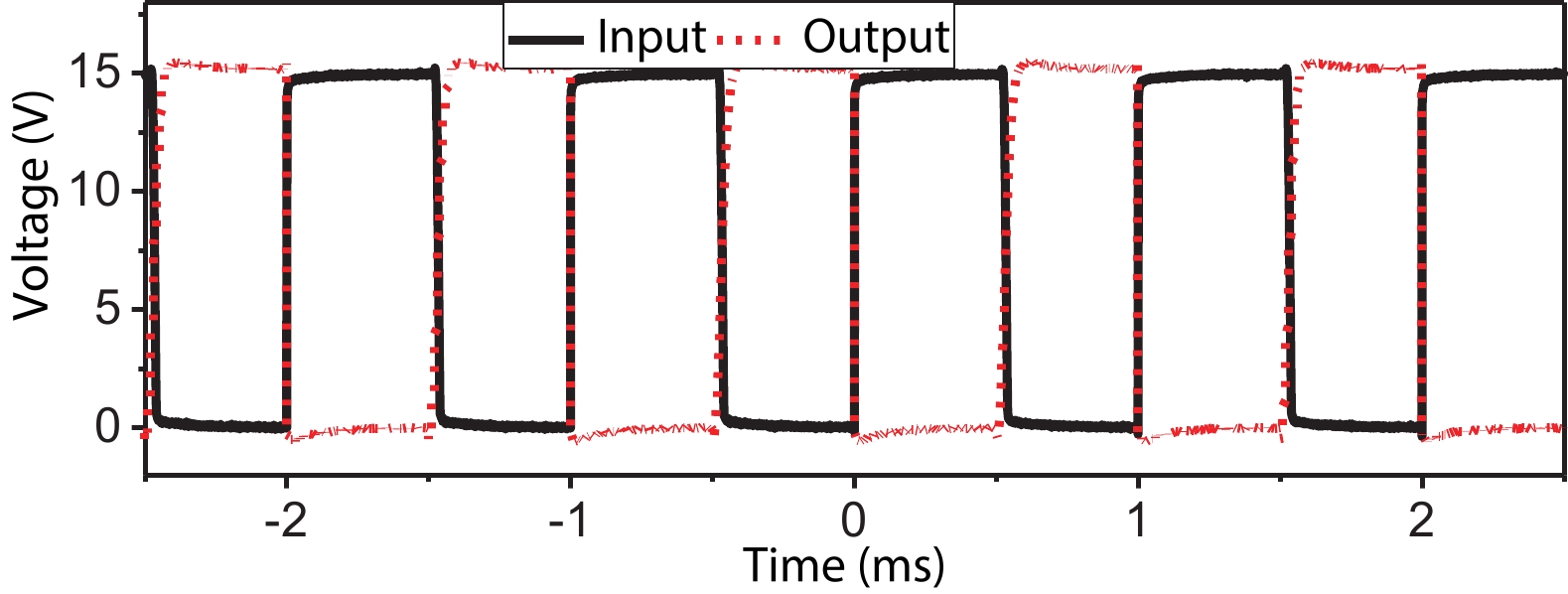
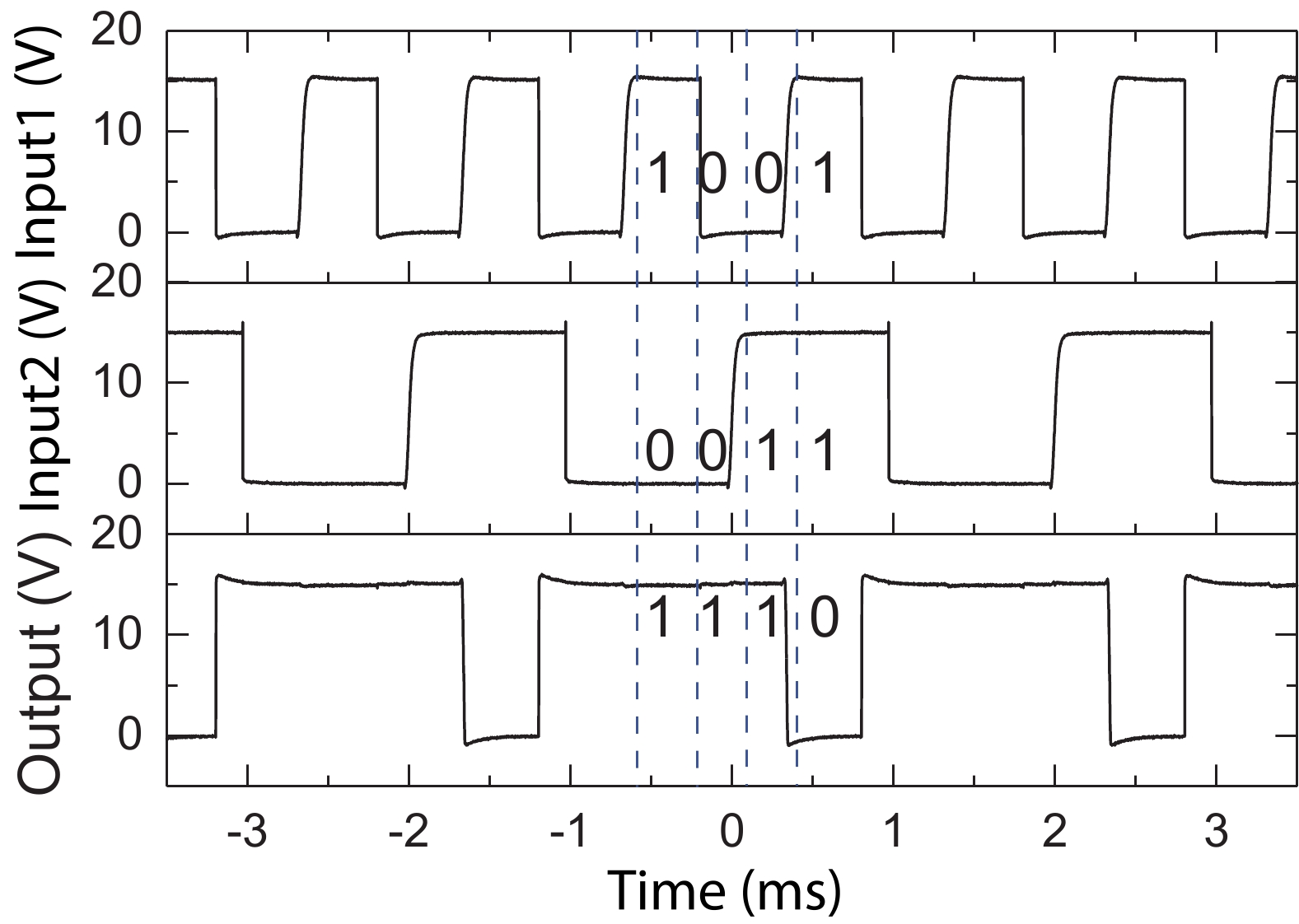
In this article, the design, fabrication and characterization of silicon carbide (SiC) complementary-metal-oxide-semiconductor (CMOS)-based integrated circuits (ICs) are presented. A metal interconnect strategy is proposed to fabricate the fundamental N-channel MOS (NMOS) and P-channel MOS (PMOS) devices that are required for the CMOS circuit configuration. Based on the mainstream 6-inch SiC wafer processing technology, the simultaneous fabrication of SiC CMOS ICs and power MOSFET is realized. Fundamental gates, such as inverter and NAND gates, are fabricated and tested. The measurement results show that the inverter and NAND gates function well. The calculated low-to-high delay (low-to-high output transition) and high-to-low delay (high-to-low output transition) are 49.9 and 90 ns, respectively.
J. Semicond.
2022, 43(8): 082802 doi: 10.1088/1674-4926/43/8/082802
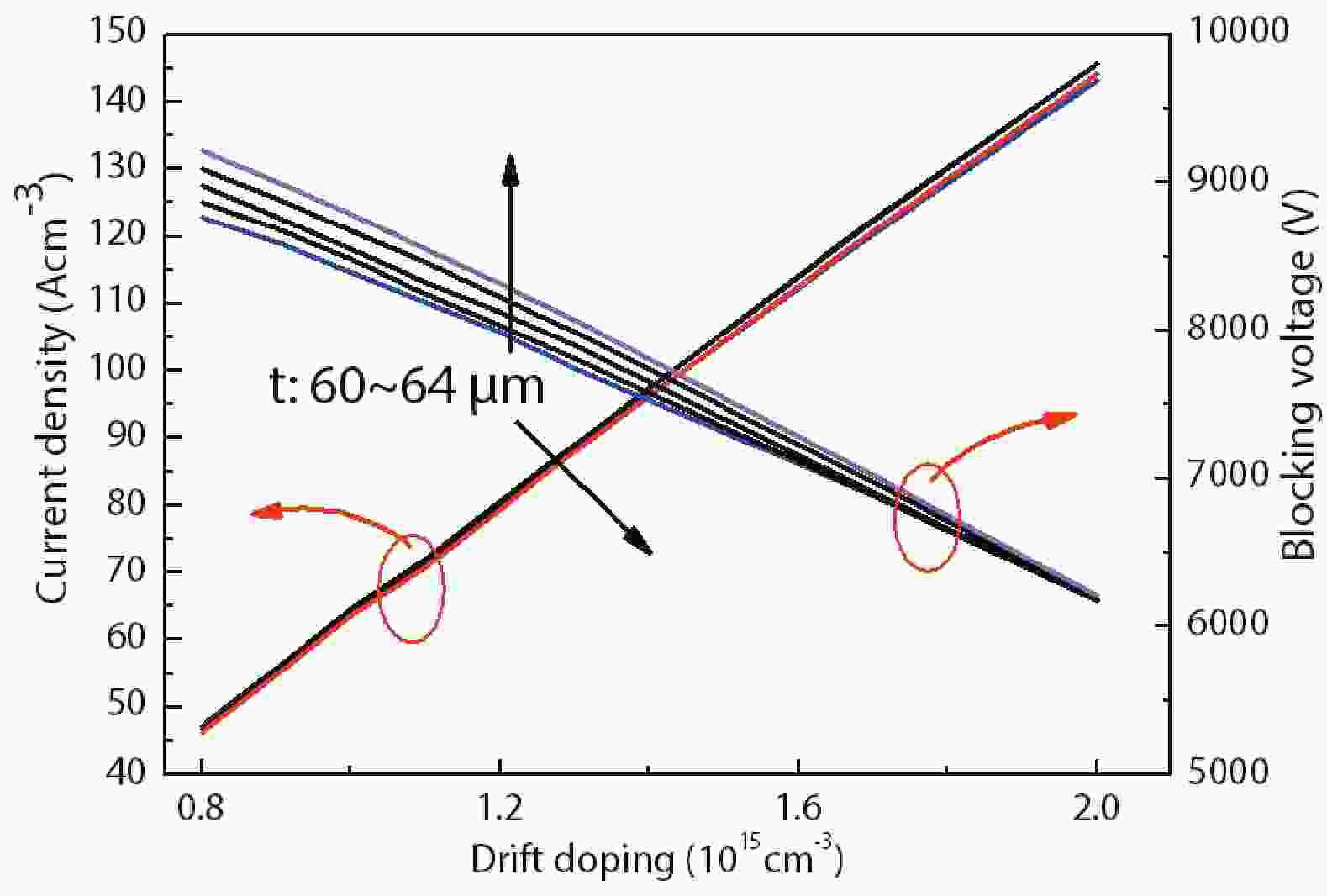
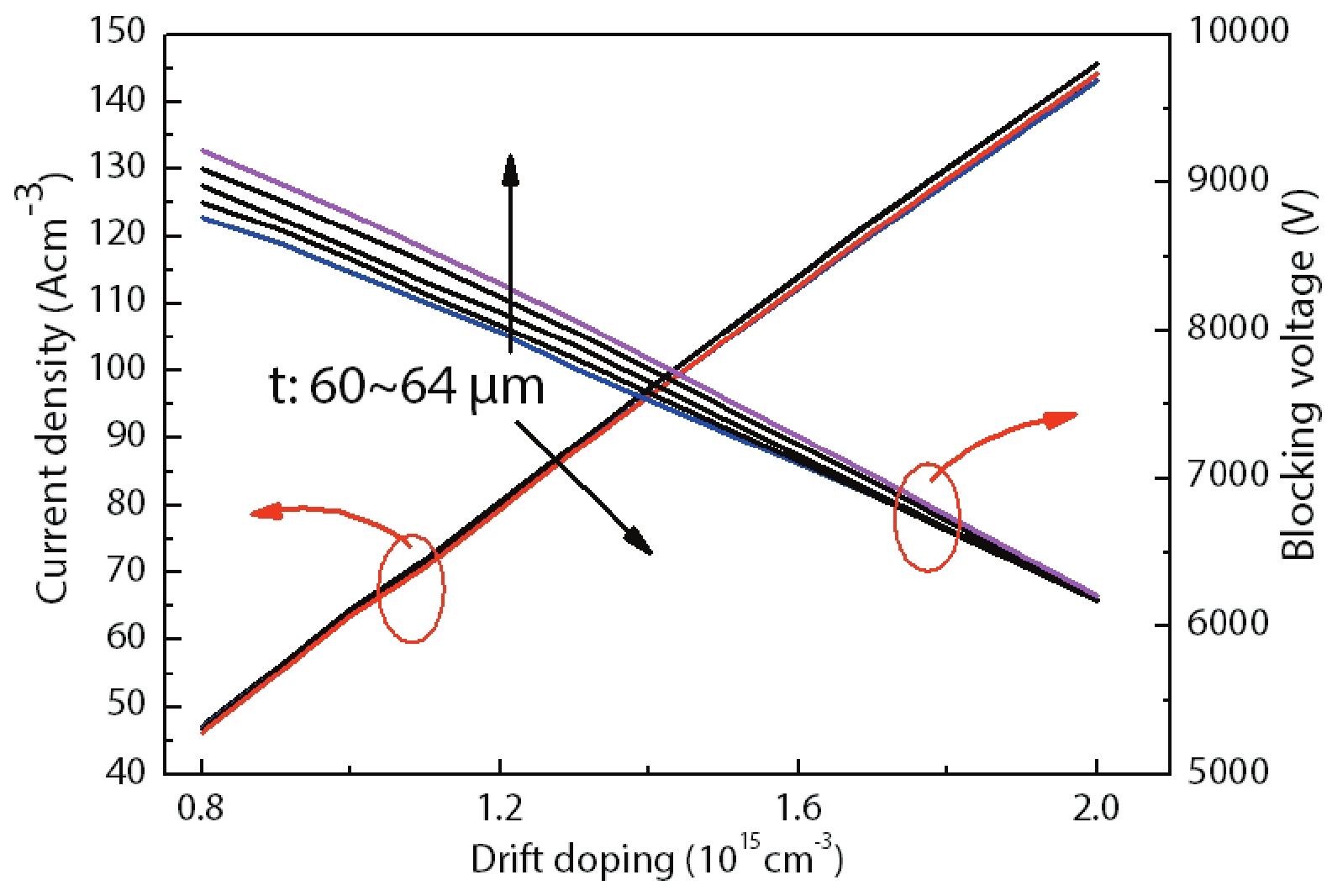
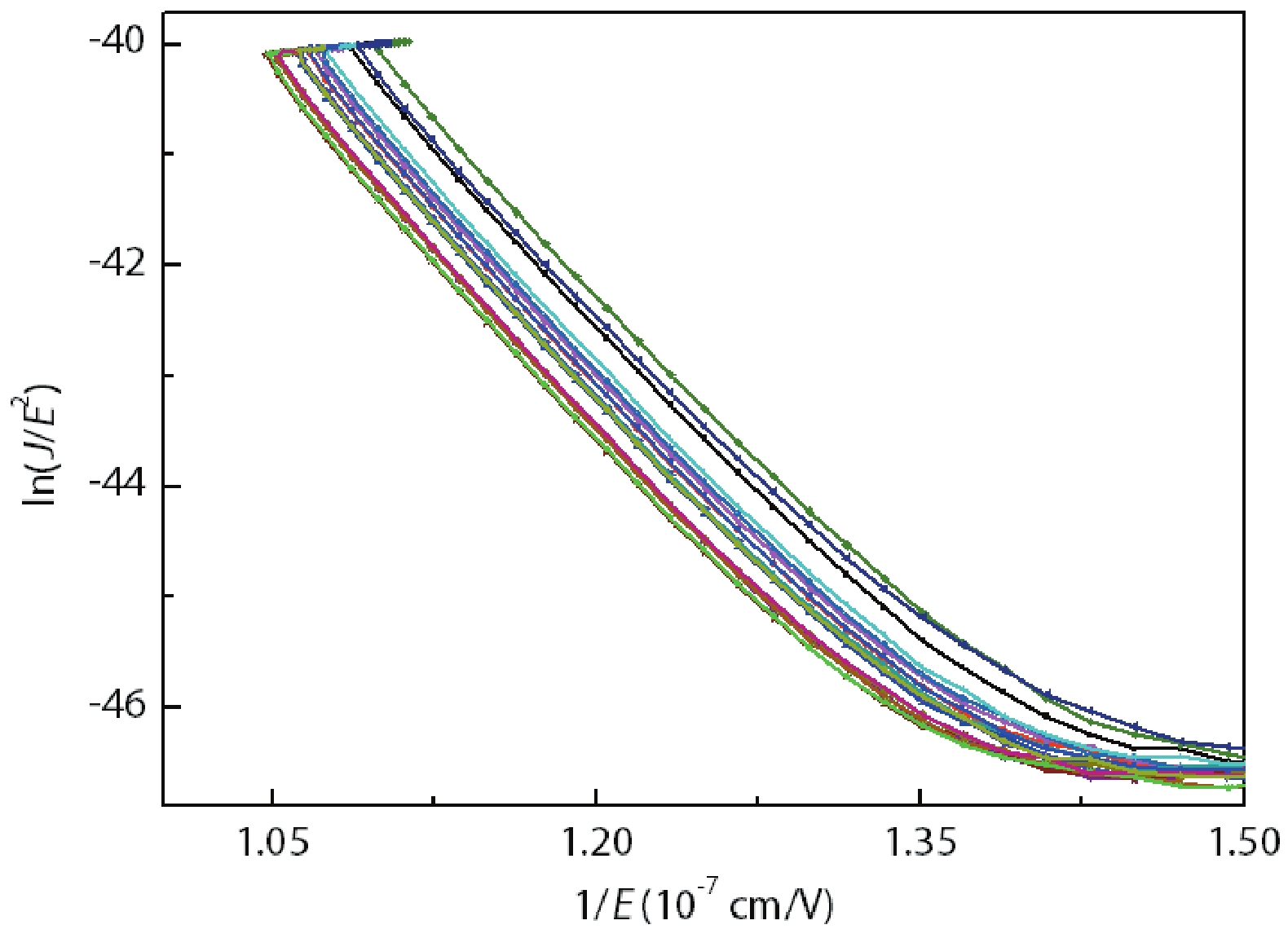
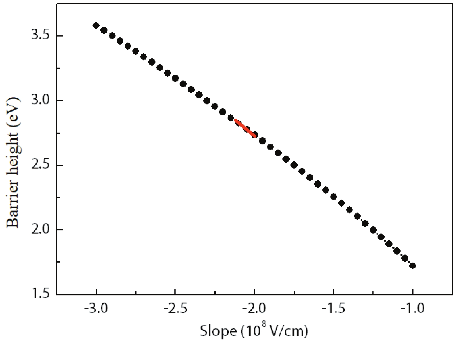
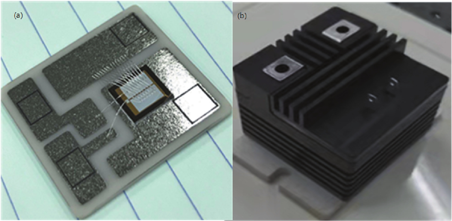
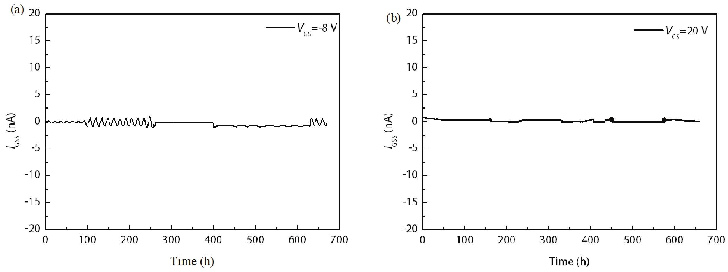
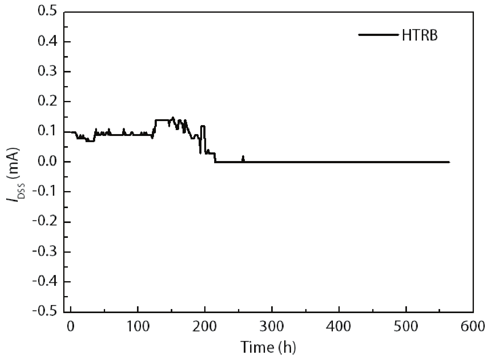
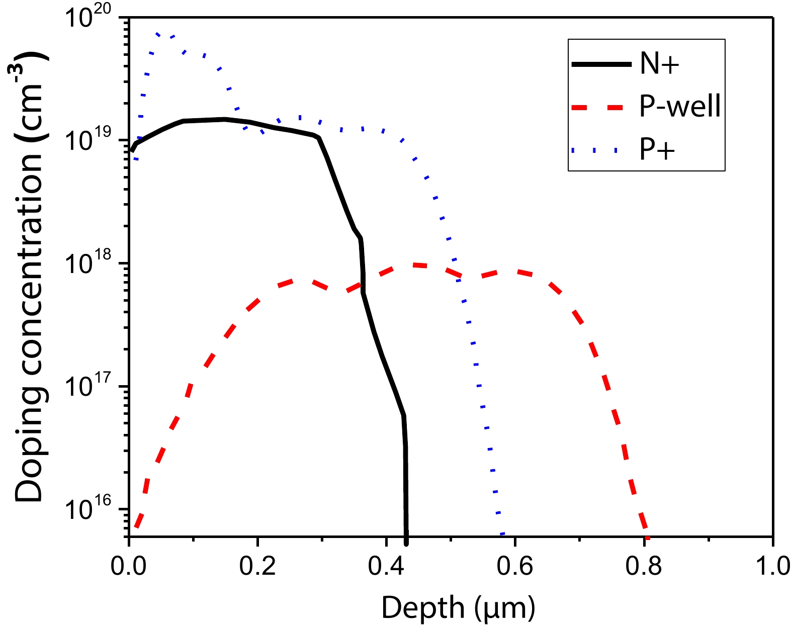
Silicon carbide (SiC) material features a wide bandgap and high critical breakdown field intensity. It also plays an important role in the high efficiency and miniaturization of power electronic equipment. It is an ideal choice for new power electronic devices, especially in smart grids and high-speed trains. In the medium and high voltage fields, SiC devices with a blocking voltage of more than 6.5 kV will have a wide range of applications. In this paper, we study the influence of epitaxial material properties on the static characteristics of 6.5 kV SiC MOSFET. 6.5 kV SiC MOSFETs with different channel lengths and JFET region widths are manufactured on three wafers and analyzed. The FN tunneling of gate oxide, HTGB and HTRB tests are performed and provide data support for the industrialization process for medium/high voltage SiC MOSFETs.