Issue Browser
Volume 44, Issue 1,
Jan 2023

J. Semicond.
2023, 44(1): 011001 doi: 10.1088/1674-4926/44/1/011001
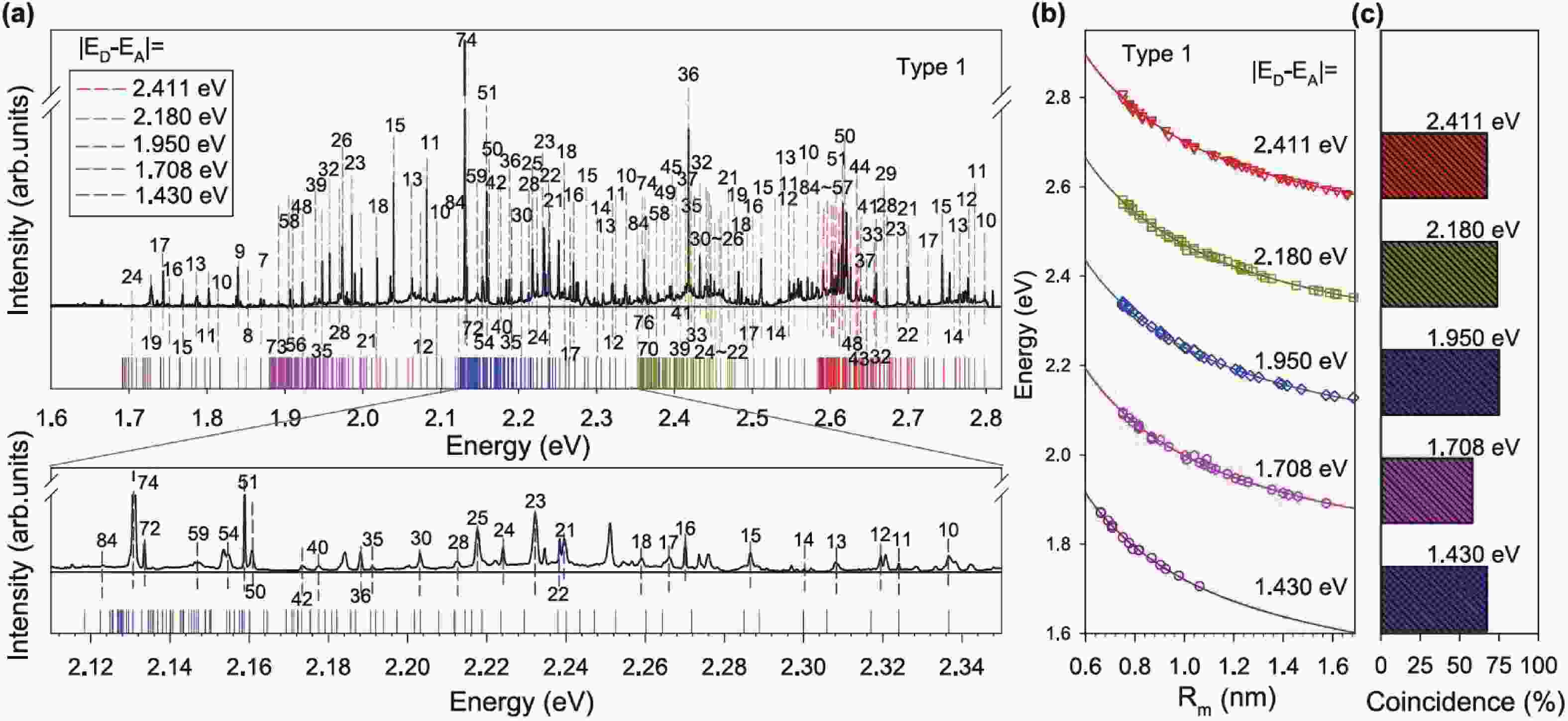
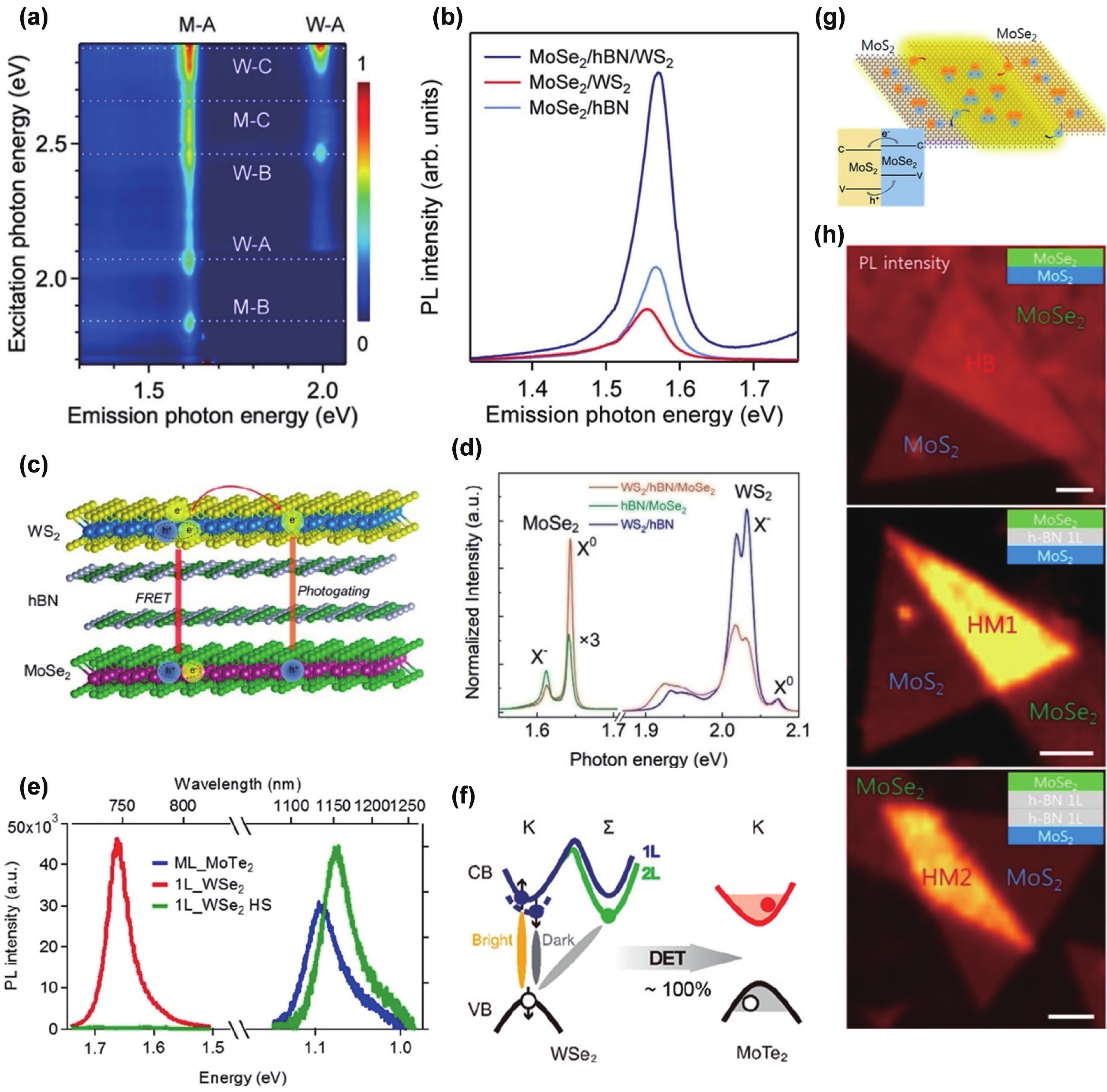
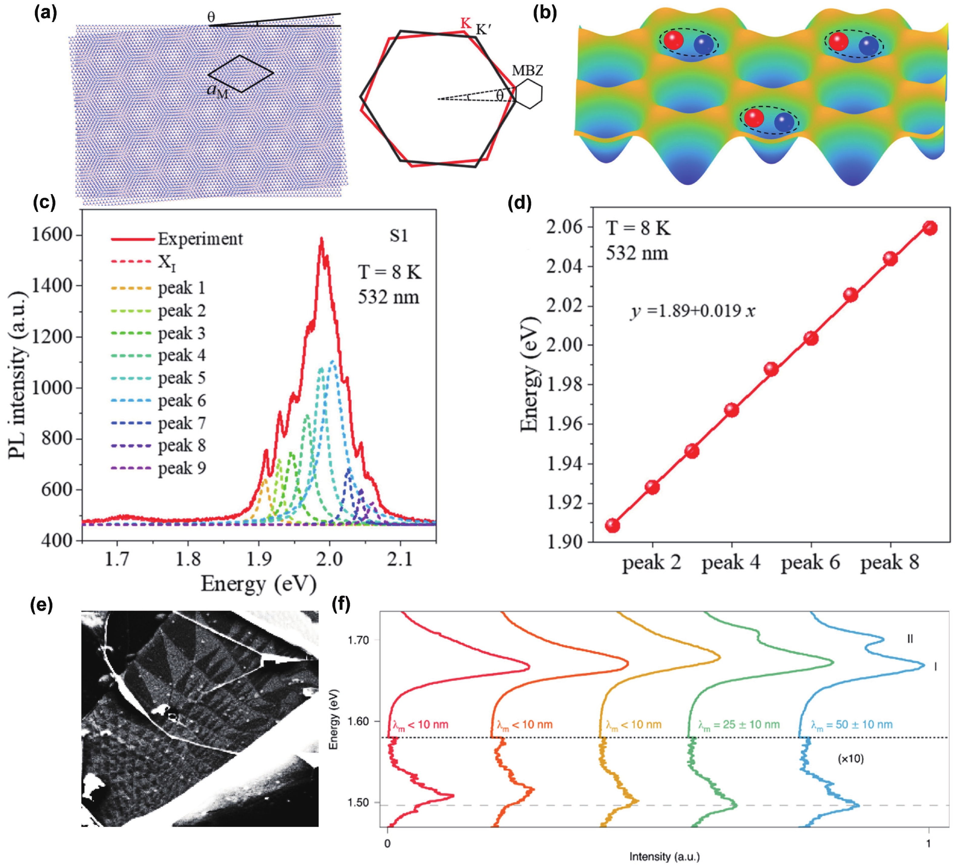
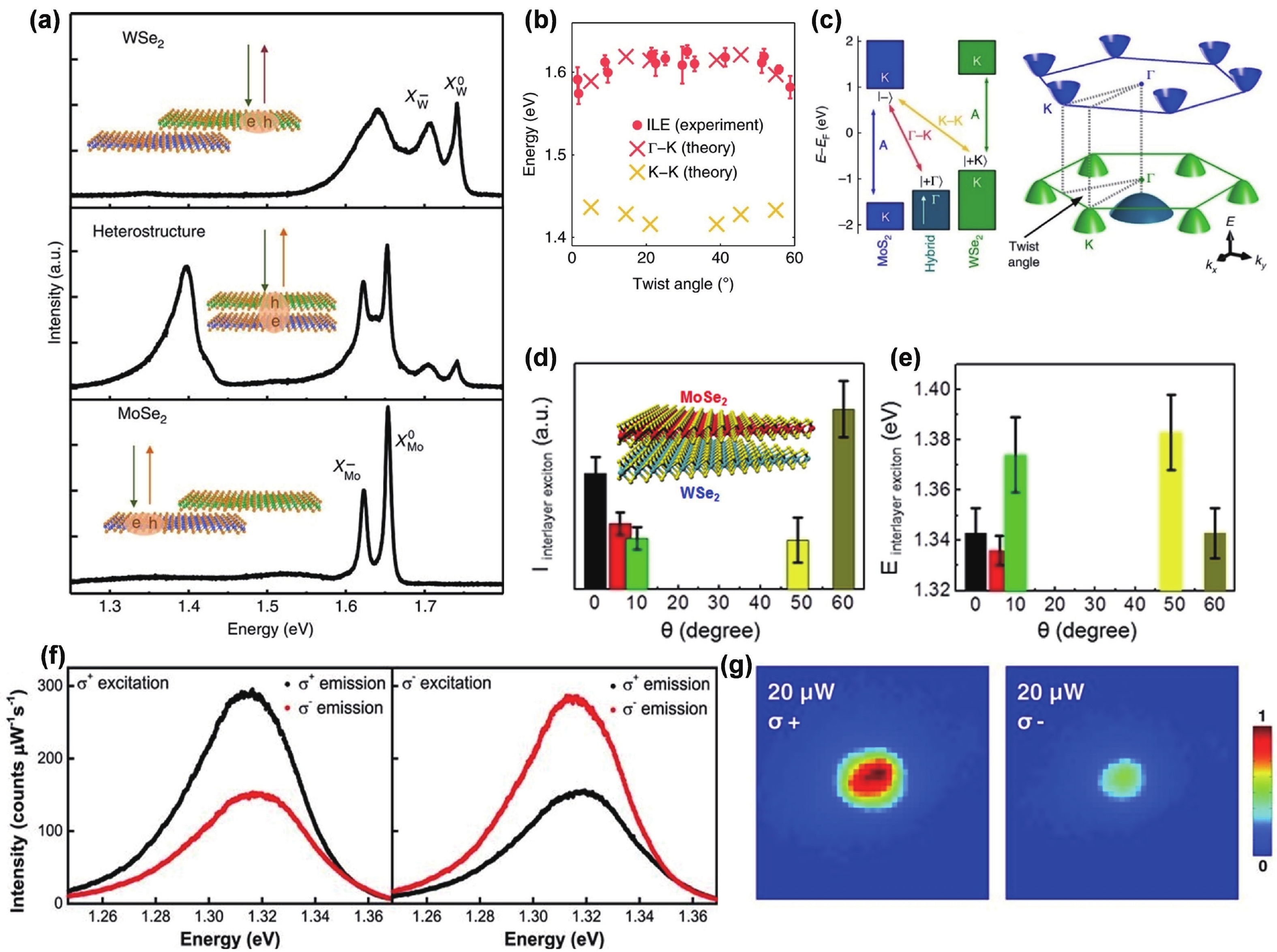
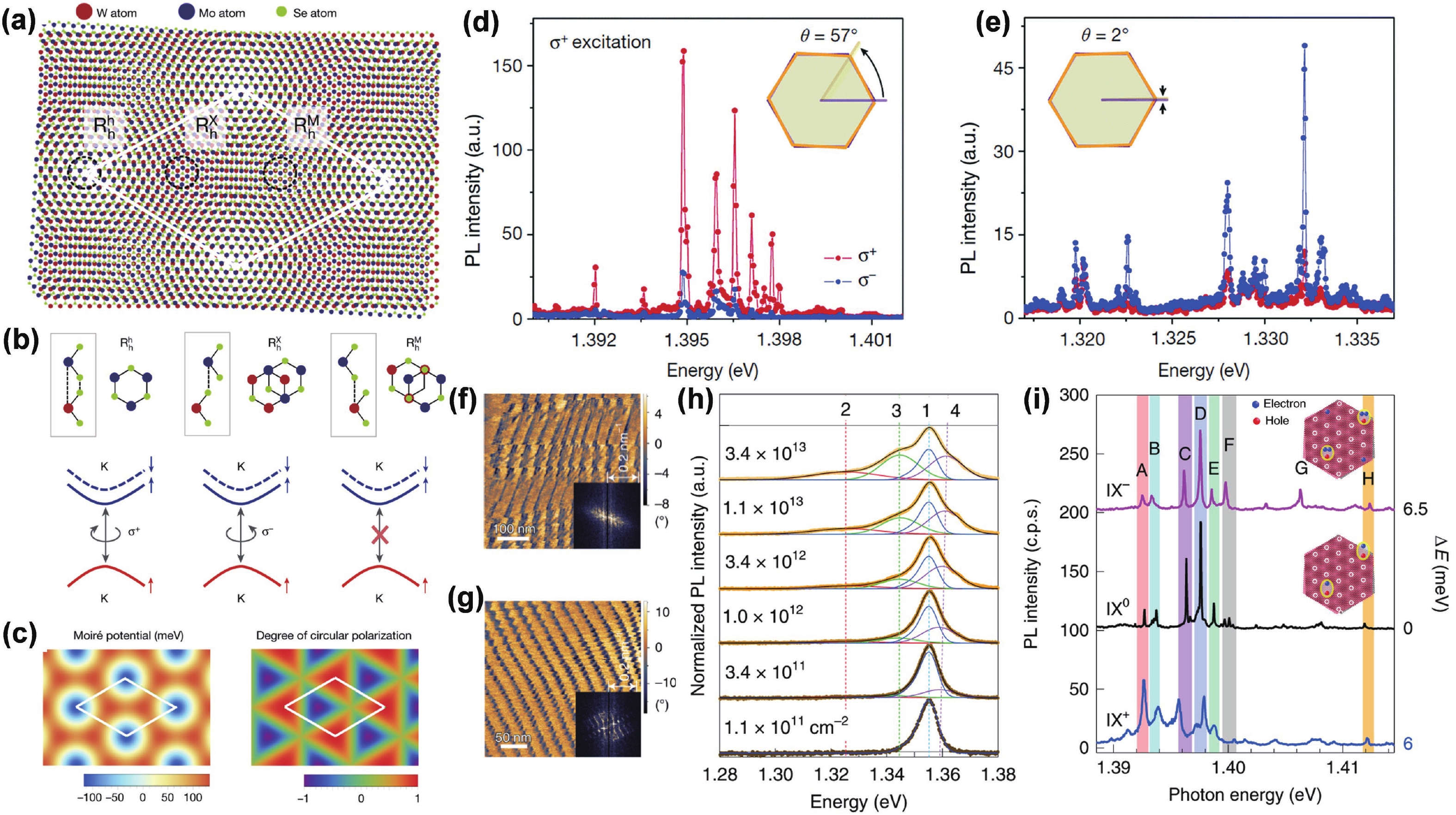
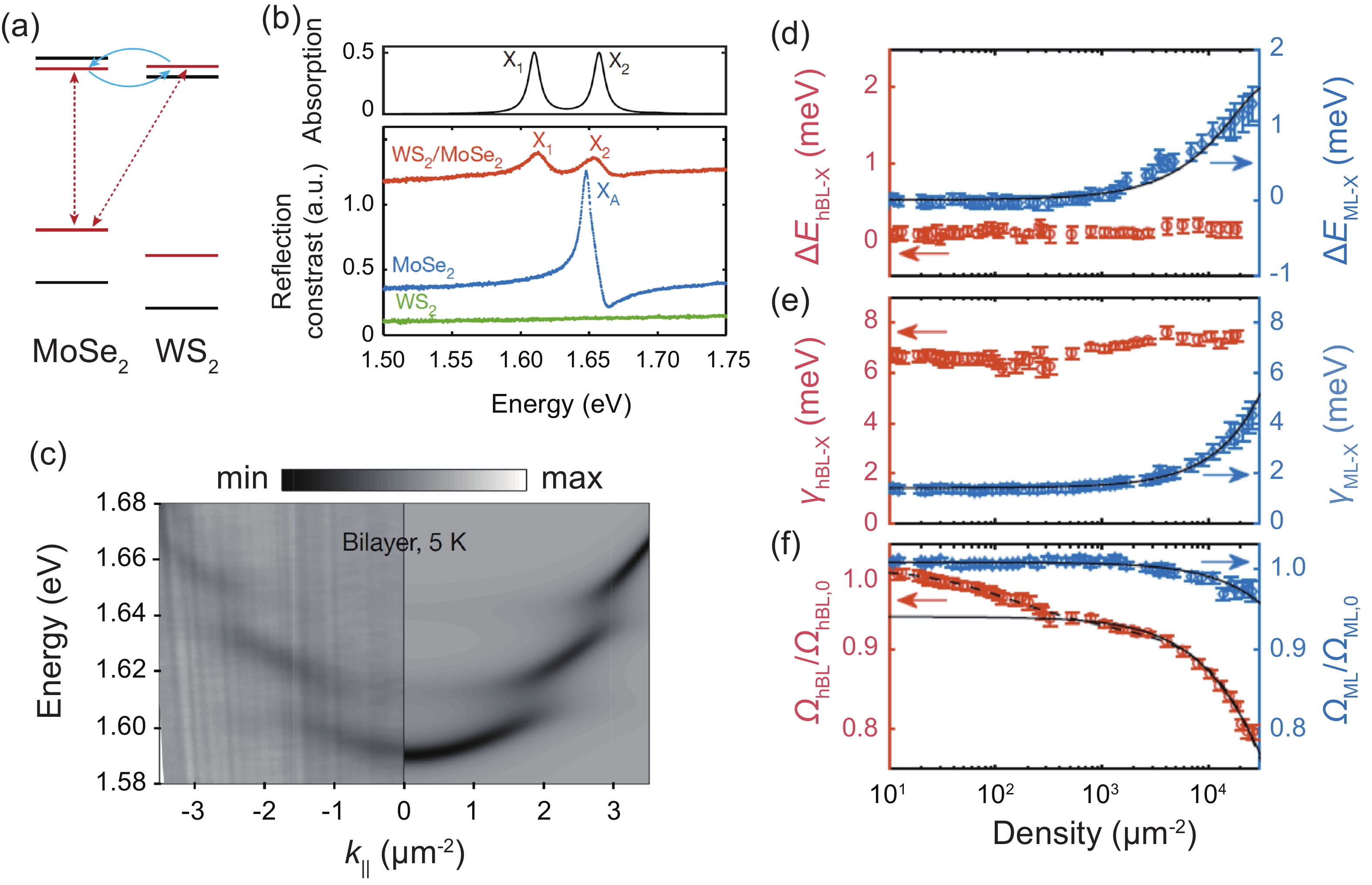
Two-dimensional (2D) semiconductors have captured broad interest as light emitters, due to their unique excitonic effects. These layer-blocks can be integrated through van der Waals assembly, i.e., fabricating homo- or heterojunctions, which show novel emission properties caused by interface engineering. In this review, we will first give an overview of the basic strategies that have been employed in interface engineering, including changing components, adjusting interlayer gap, and tuning twist angle. By modifying the interfacial factors, novel emission properties of emerging excitons are unveiled and discussed. Generally, well-tailored interfacial energy transfer and charge transfer within a 2D heterostructure cause static modulation of the brightness of intralayer excitons. As a special case, dynamically correlated dual-color emission in weakly-coupled bilayers will be introduced, which originates from intermittent interlayer charge transfer. For homobilayers and type Ⅱ heterobilayers, interlayer excitons with electrons and holes residing in neighboring layers are another important topic in this review. Moreover, the overlap of two crystal lattices forms moiré patterns with a relatively large period, taking effect on intralayer and interlayer excitons. Particularly, theoretical and experimental progresses on spatially modulated moiré excitons with ultra-sharp linewidth and quantum emission properties will be highlighted. Moiré quantum emitter provides uniform and integratable arrays of single photon emitters that are previously inaccessible, which is essential in quantum many-body simulation and quantum information processing. Benefiting from the optically addressable spin and valley indices, 2D heterostructures have become an indispensable platform for investigating exciton physics, designing and integrating novel concept emitters.


J. Semicond.
2023, 44(1): 011002 doi: 10.1088/1674-4926/44/1/011002
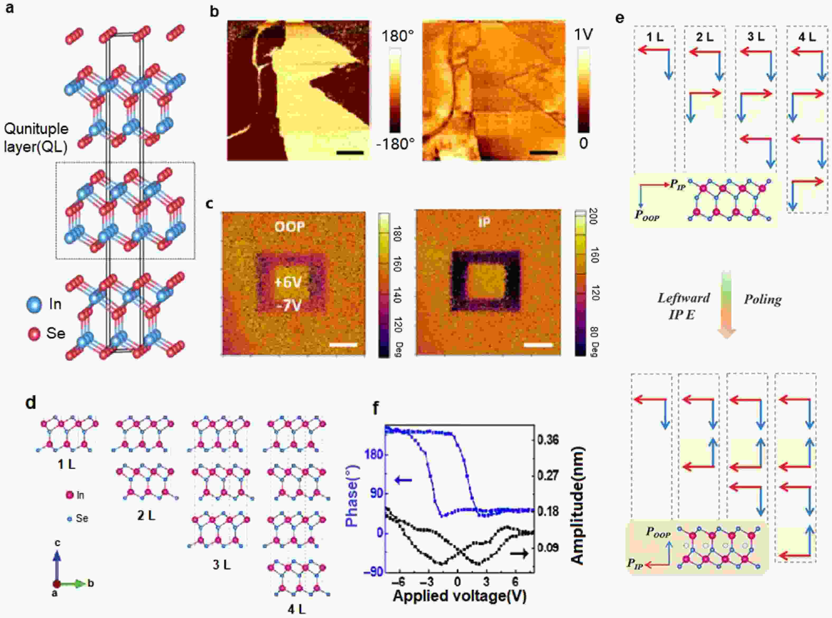
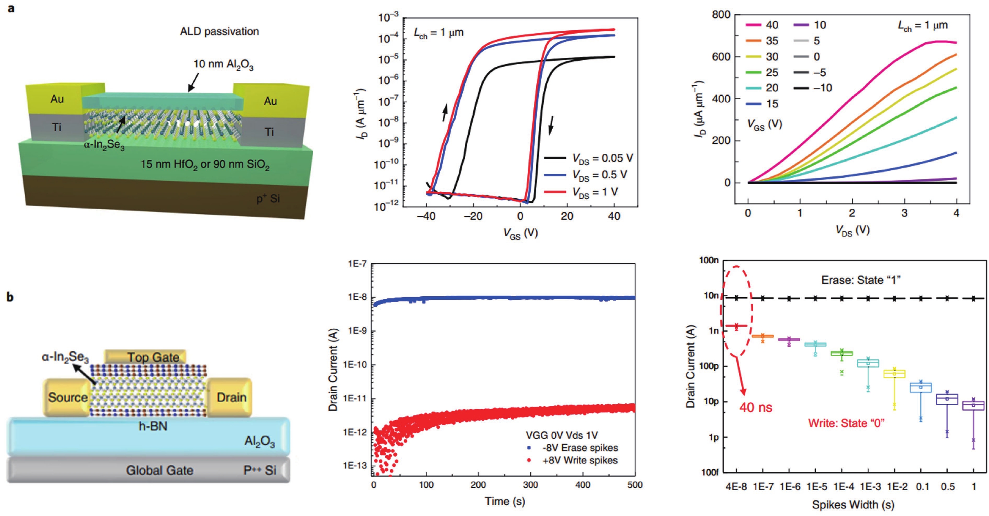
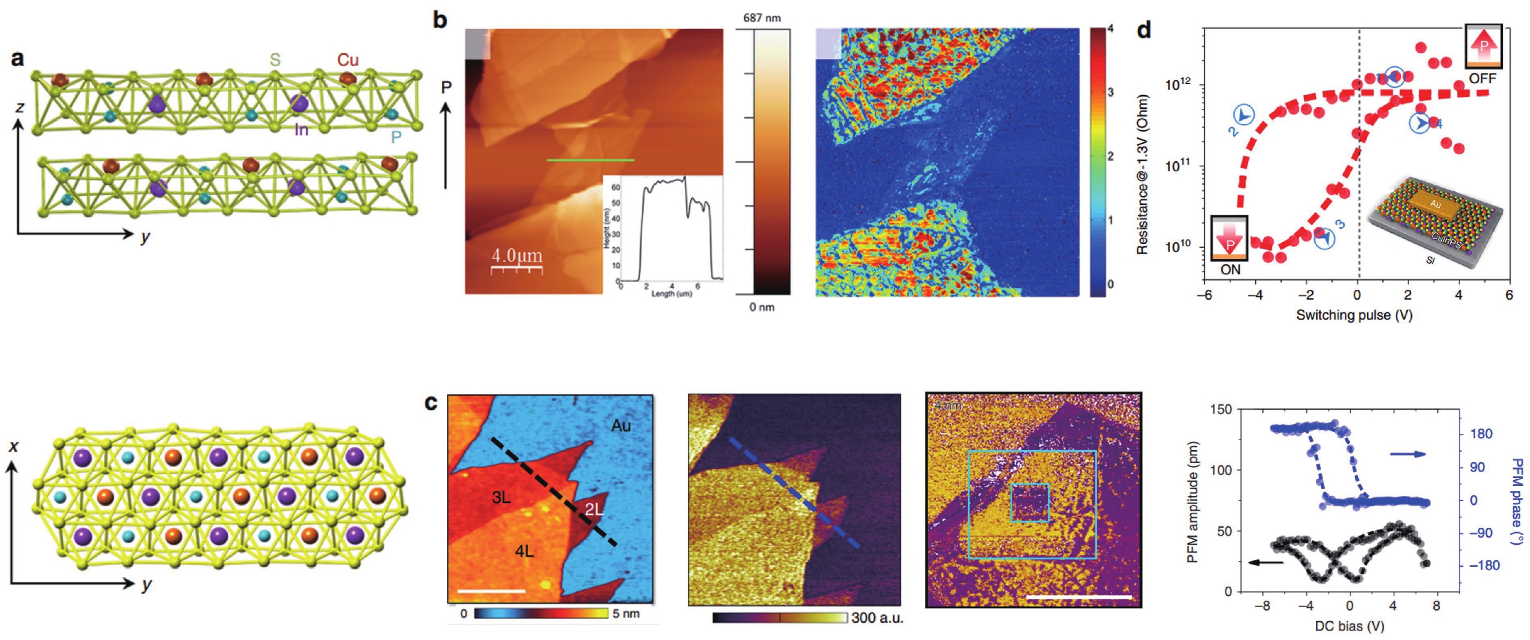
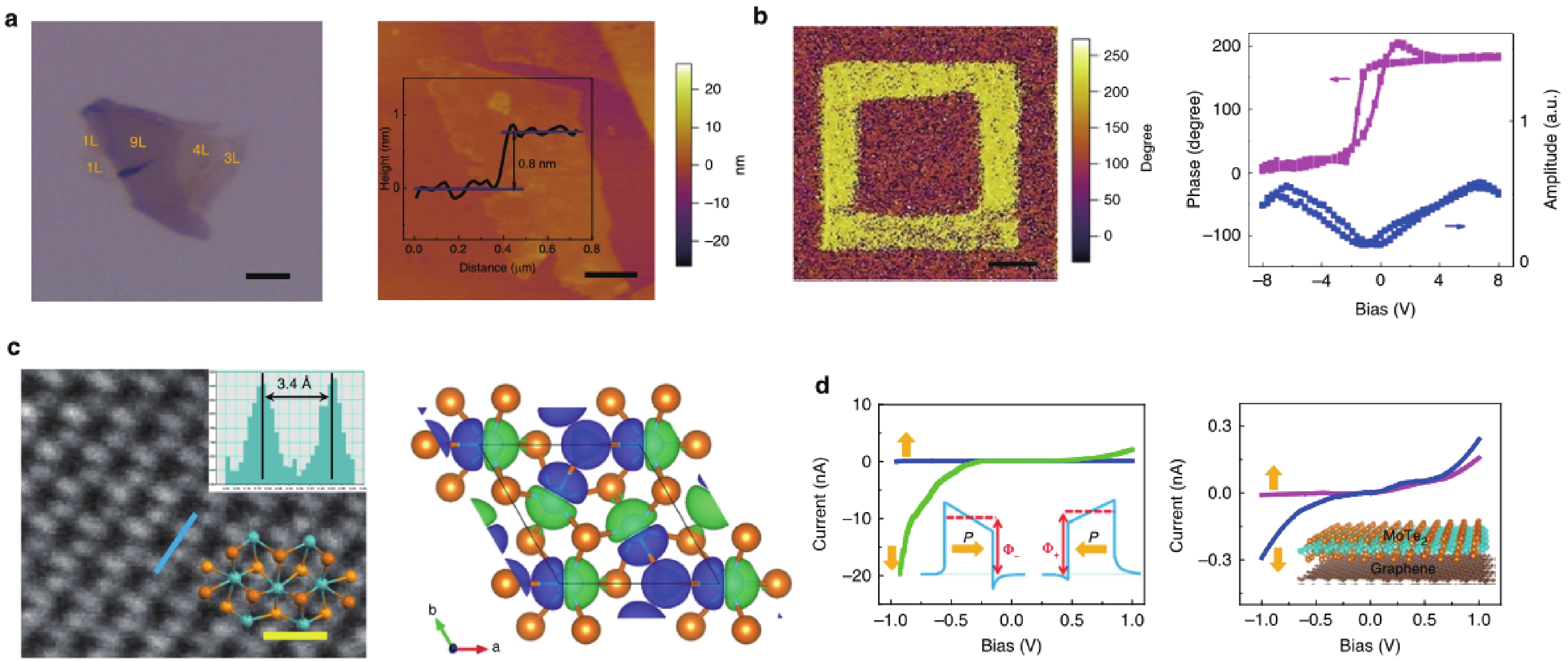
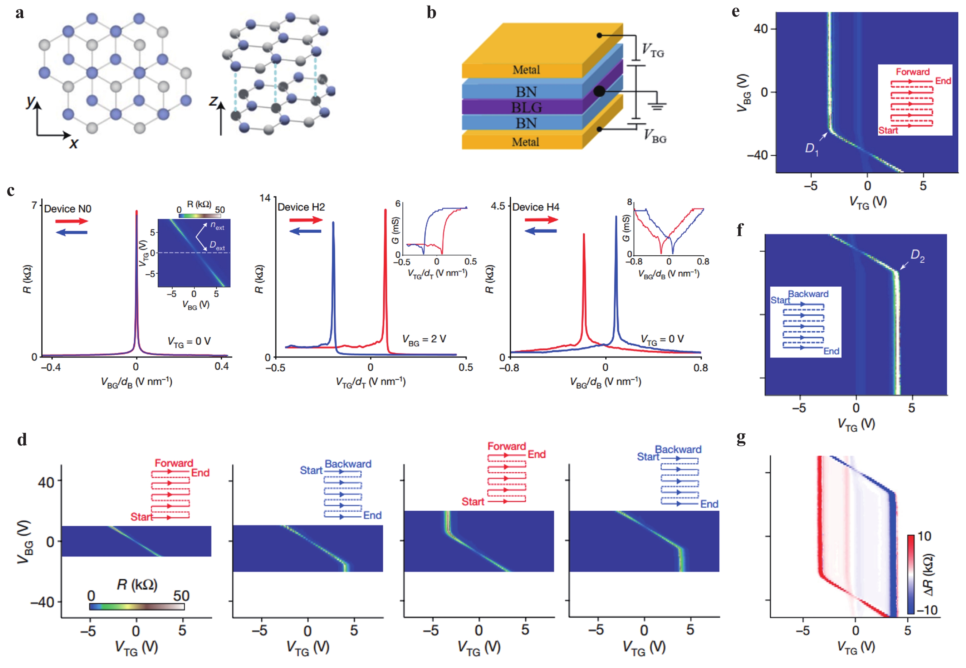
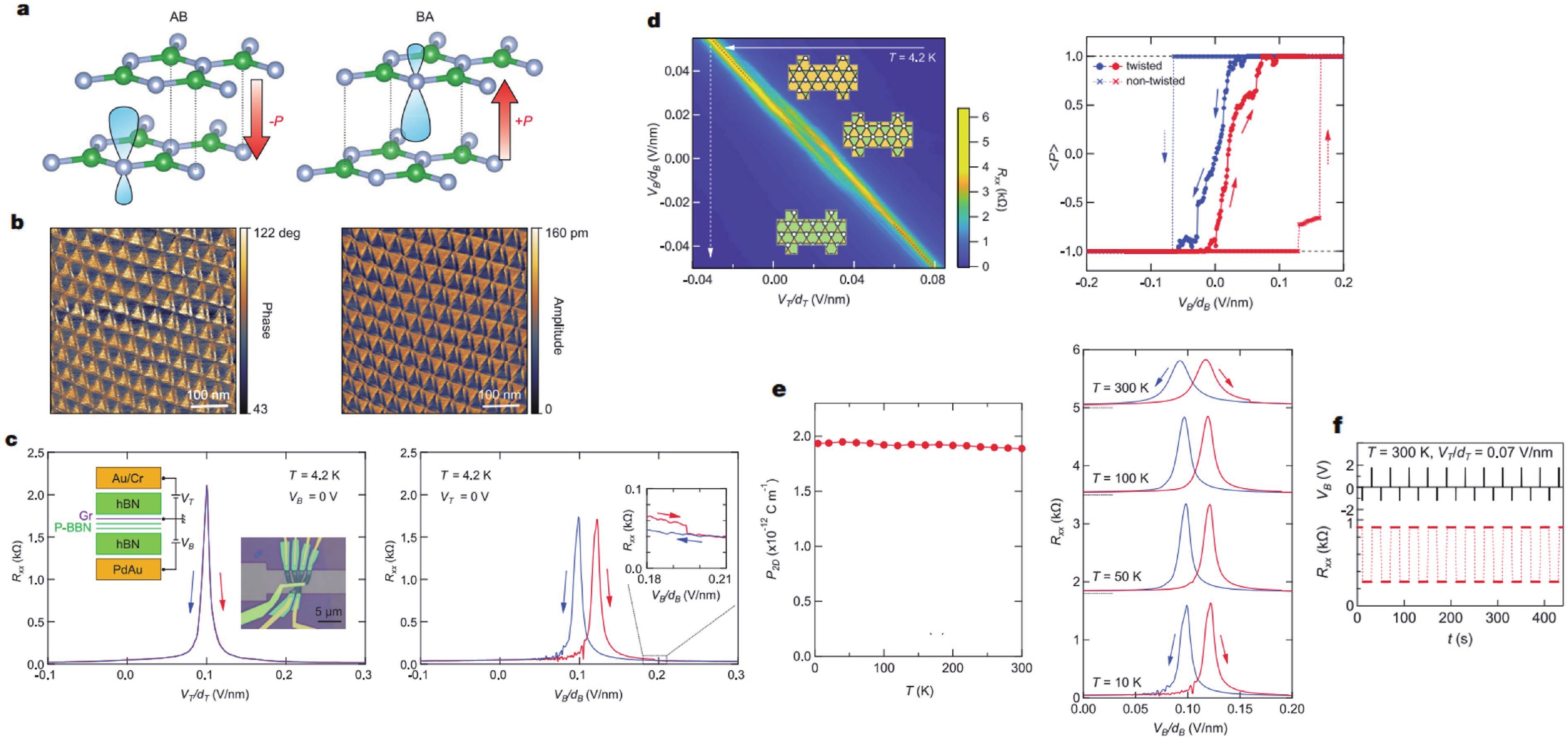
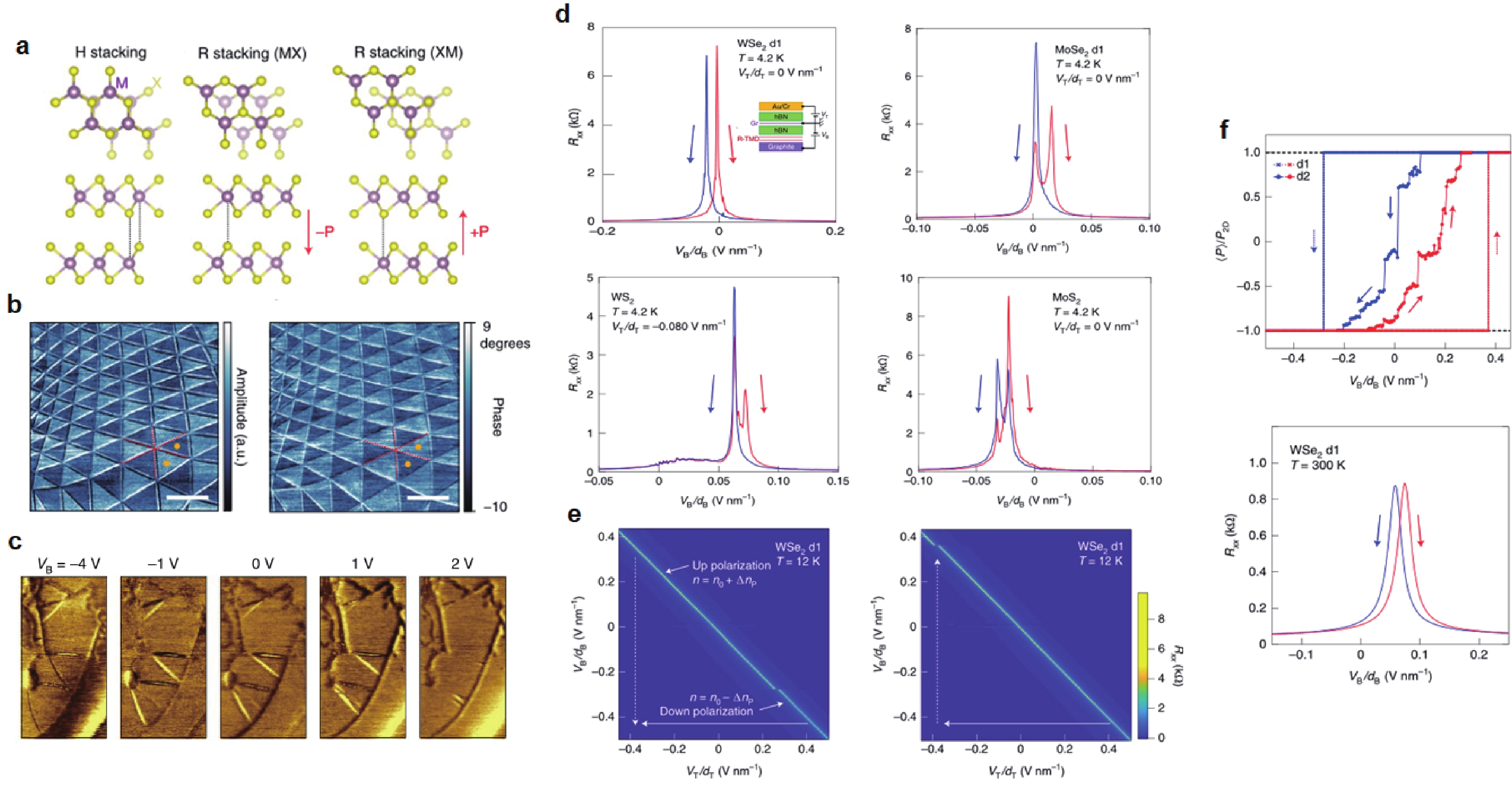
Since the beginning of research on two-dimensional (2D) materials, a few numbers of 2D ferroelectric materials have been predicted or experimentally confirmed, but 2D ferroelectrics as necessary functional materials are greatly important in developing future electronic devices. Recent breakthroughs in 2D ferroelectric materials are impressive, and the physical and structural properties of twisted 2D ferroelectrics, a new type of ferroelectric structure by rotating alternating monolayers to form an angle with each other, have attracted widespread interest and discussion. Here, we review the latest research on twisted 2D ferroelectrics, including Bernal-stacked bilayer graphene/BN, bilayer boron nitride, and transition metal dichalcogenides. Finally, we prospect the development of twisted 2D ferroelectrics and discuss the challenges and future of 2D ferroelectric materials.

J. Semicond.
2023, 44(1): 011901 doi: 10.1088/1674-4926/44/1/011901
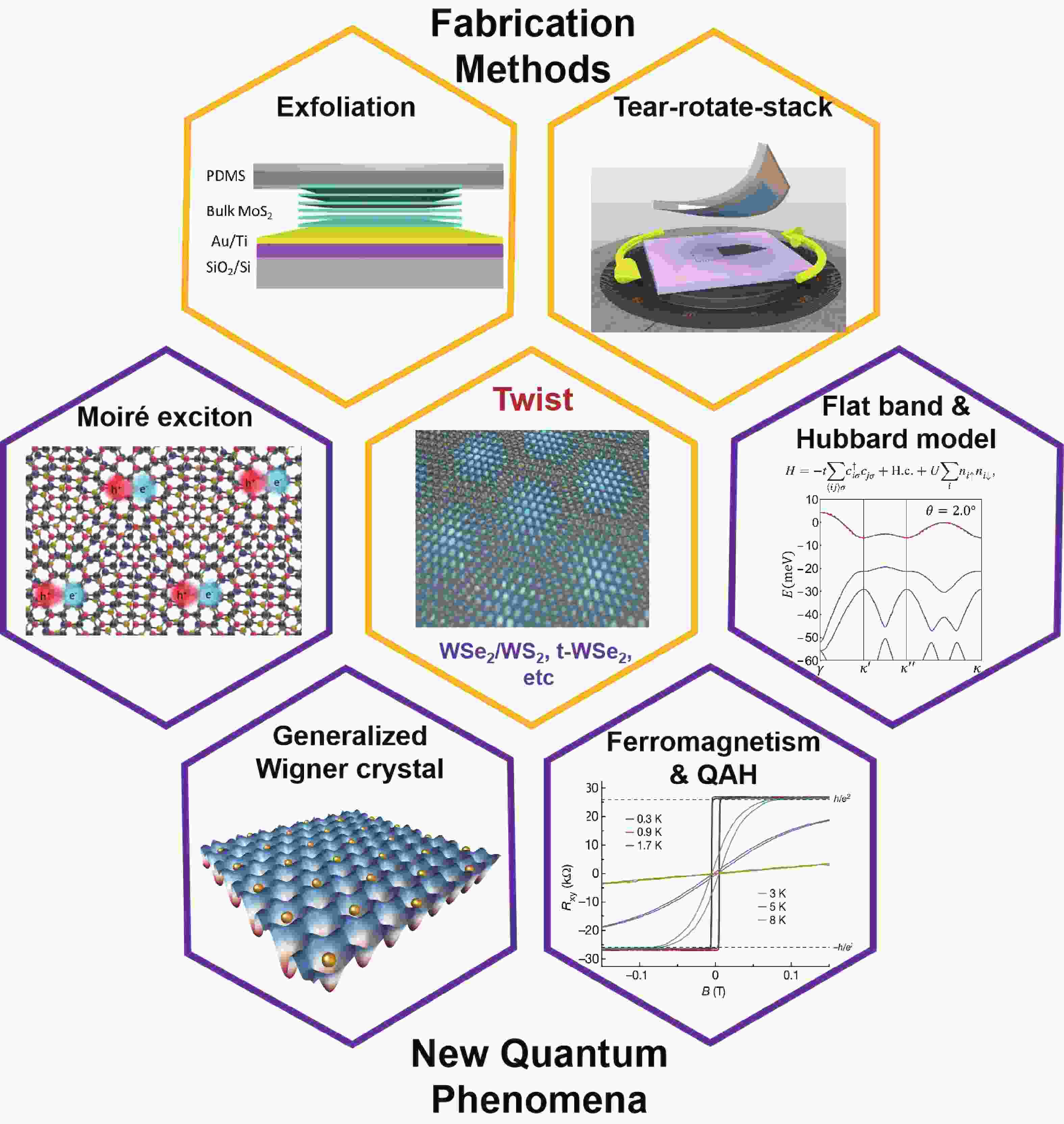
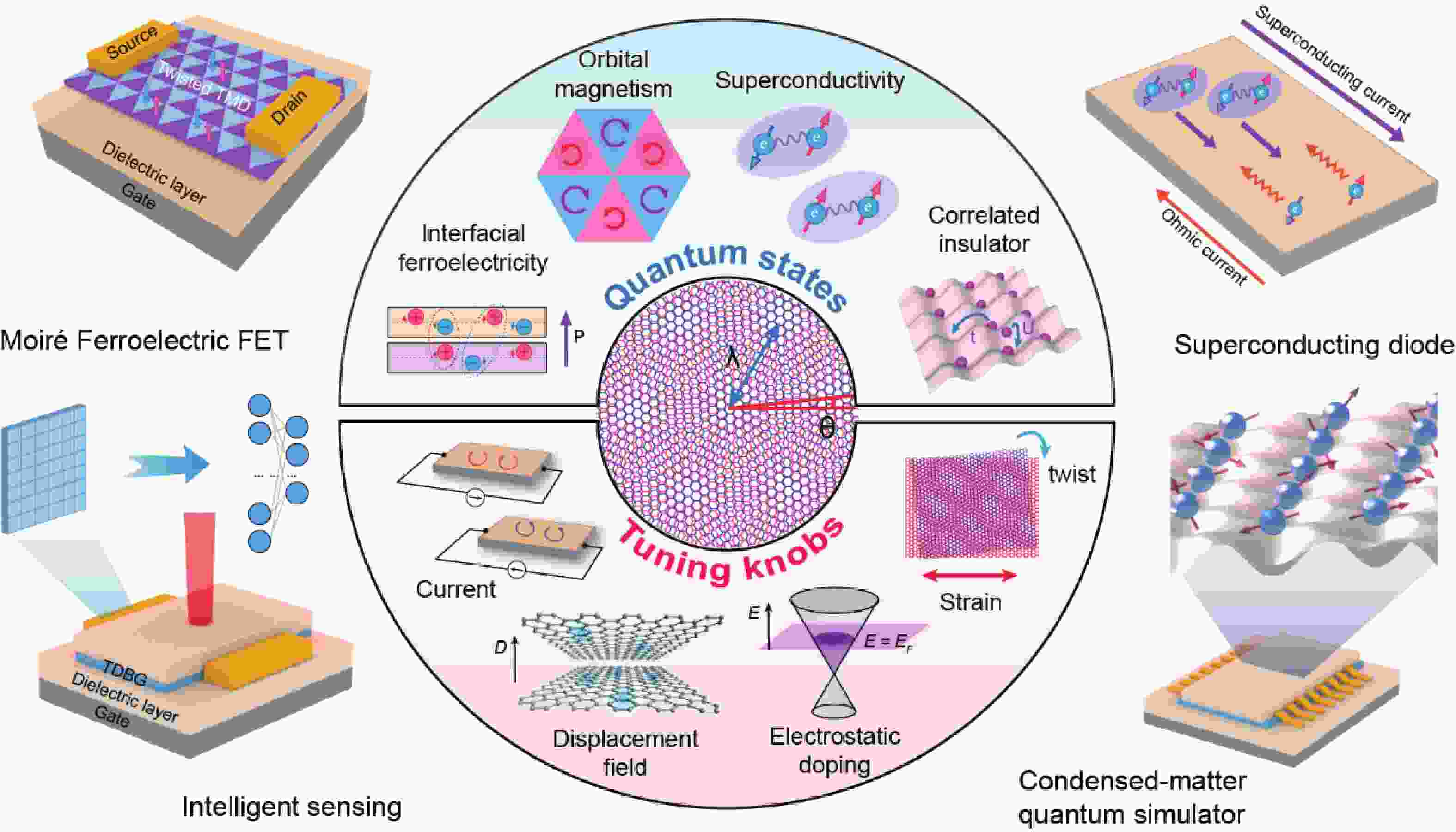
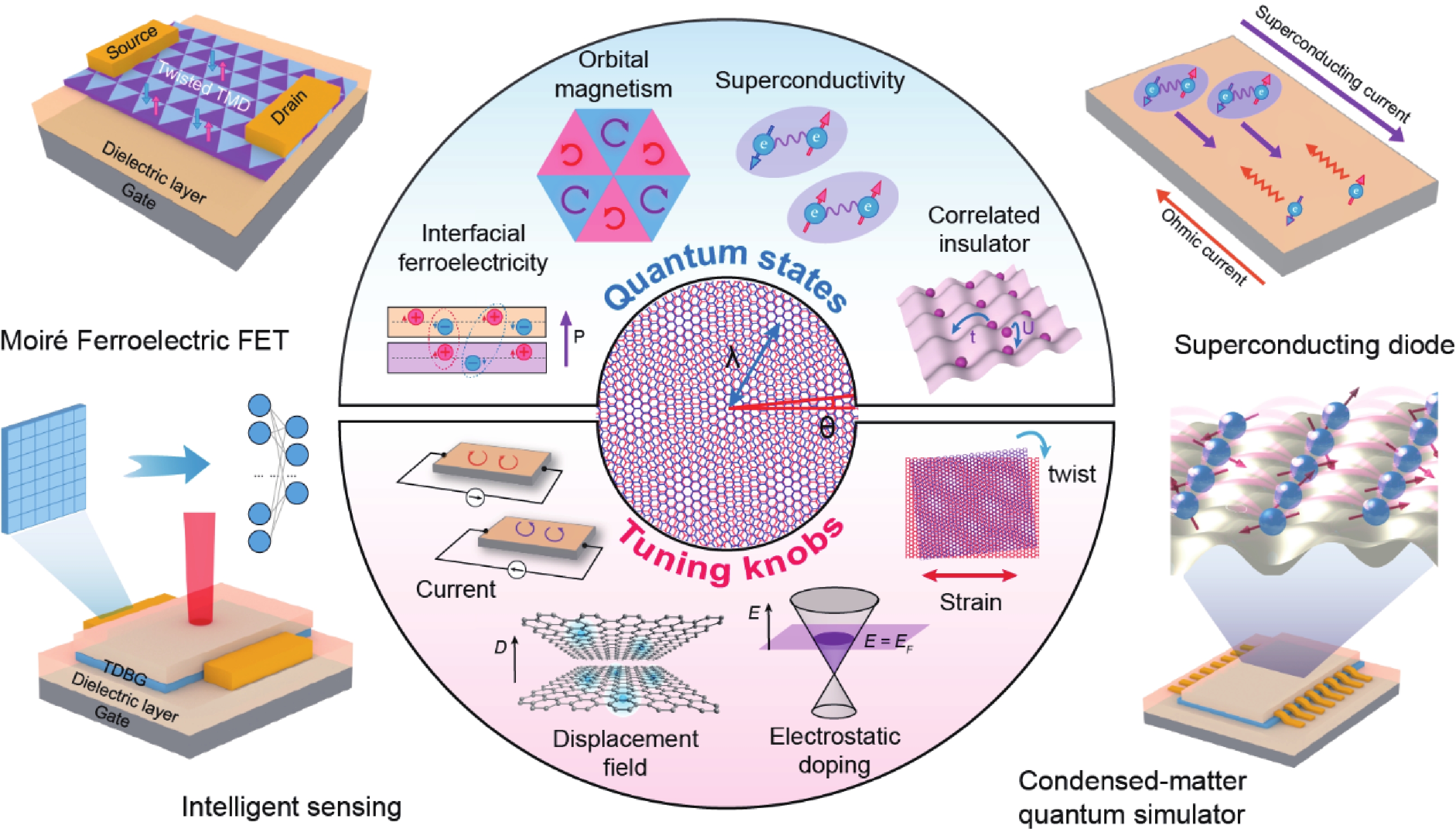
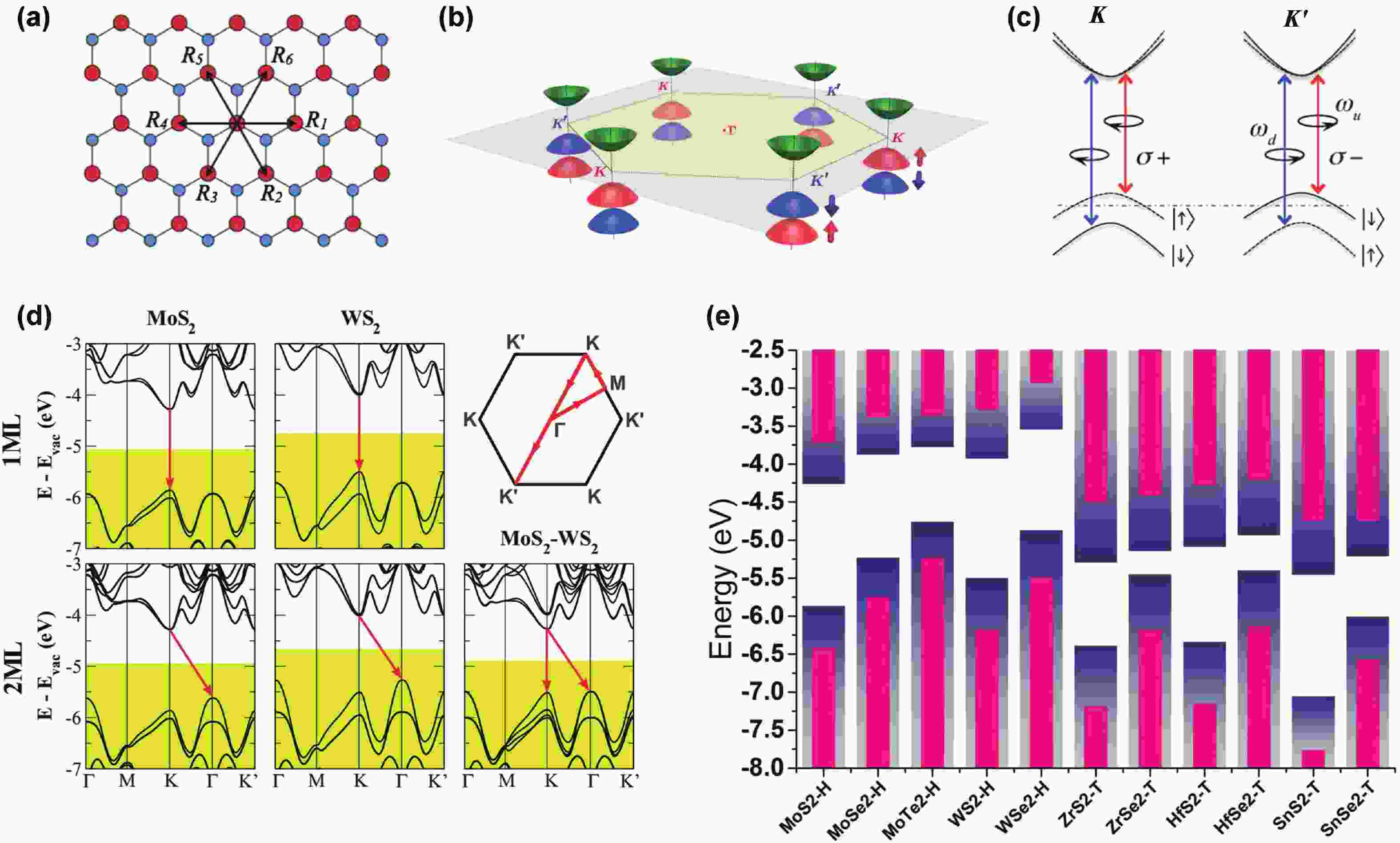
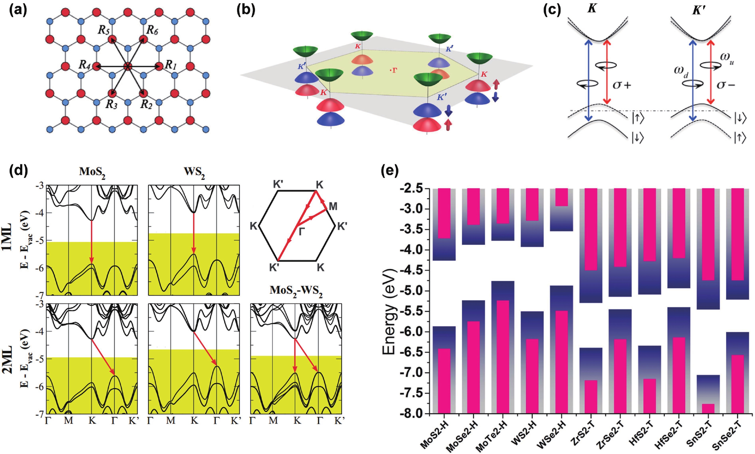
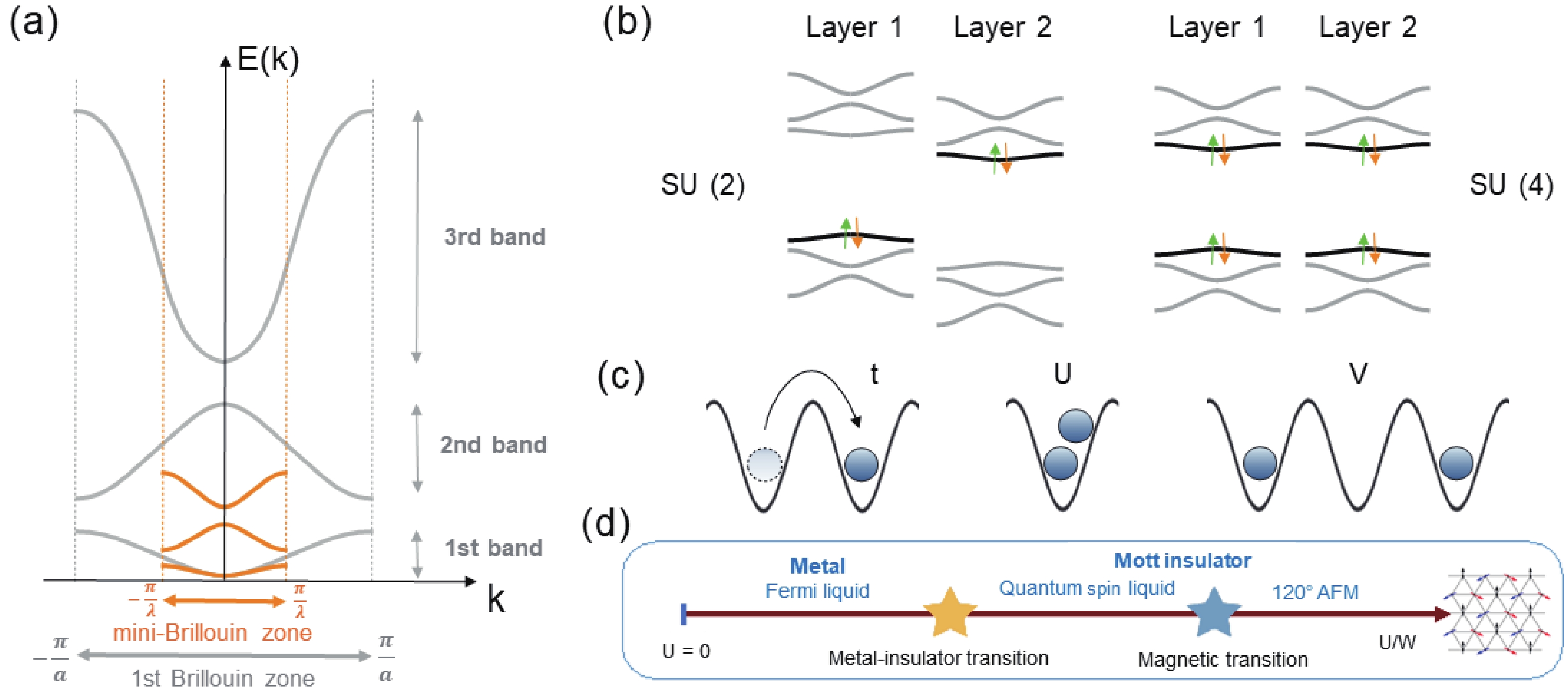
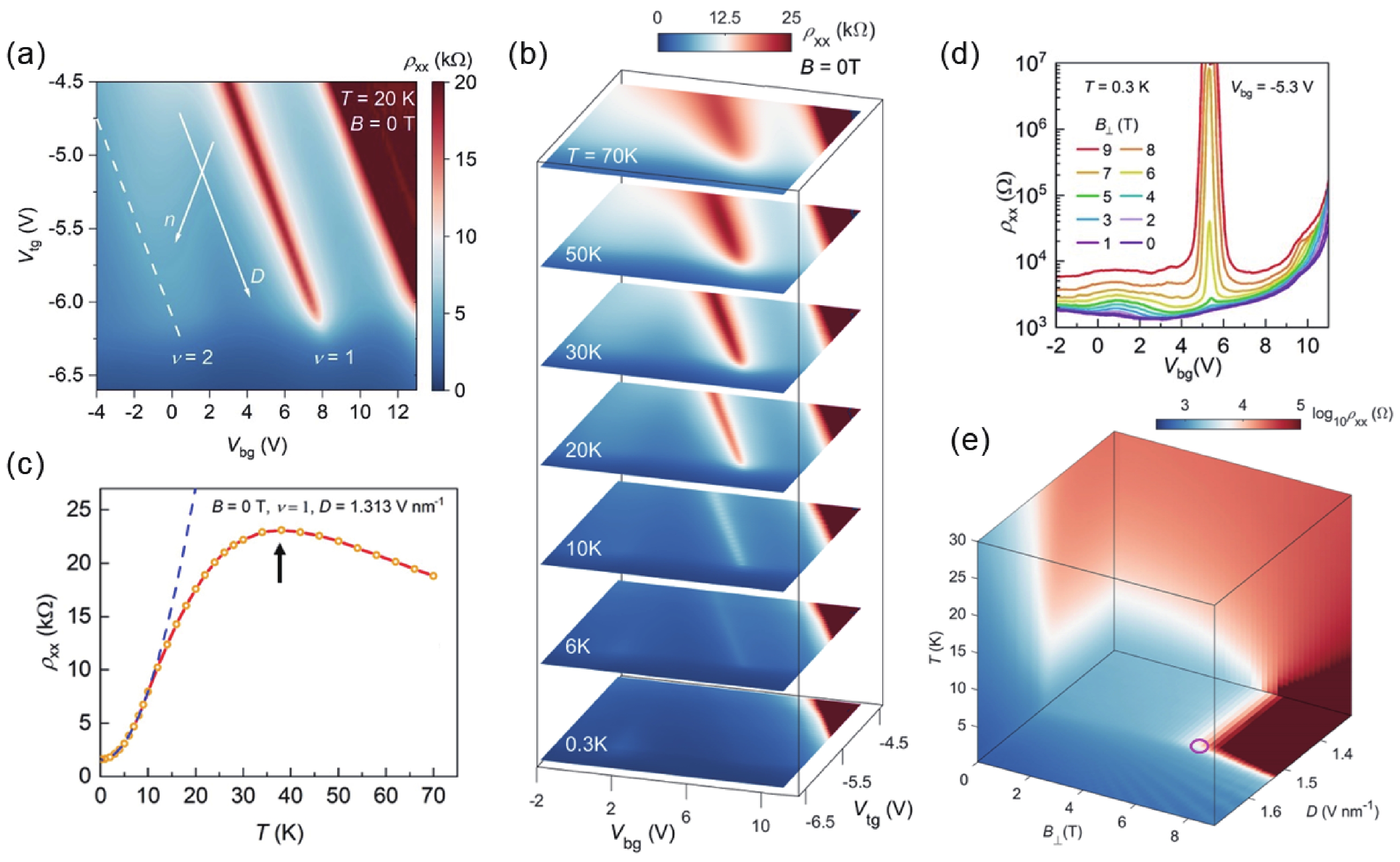
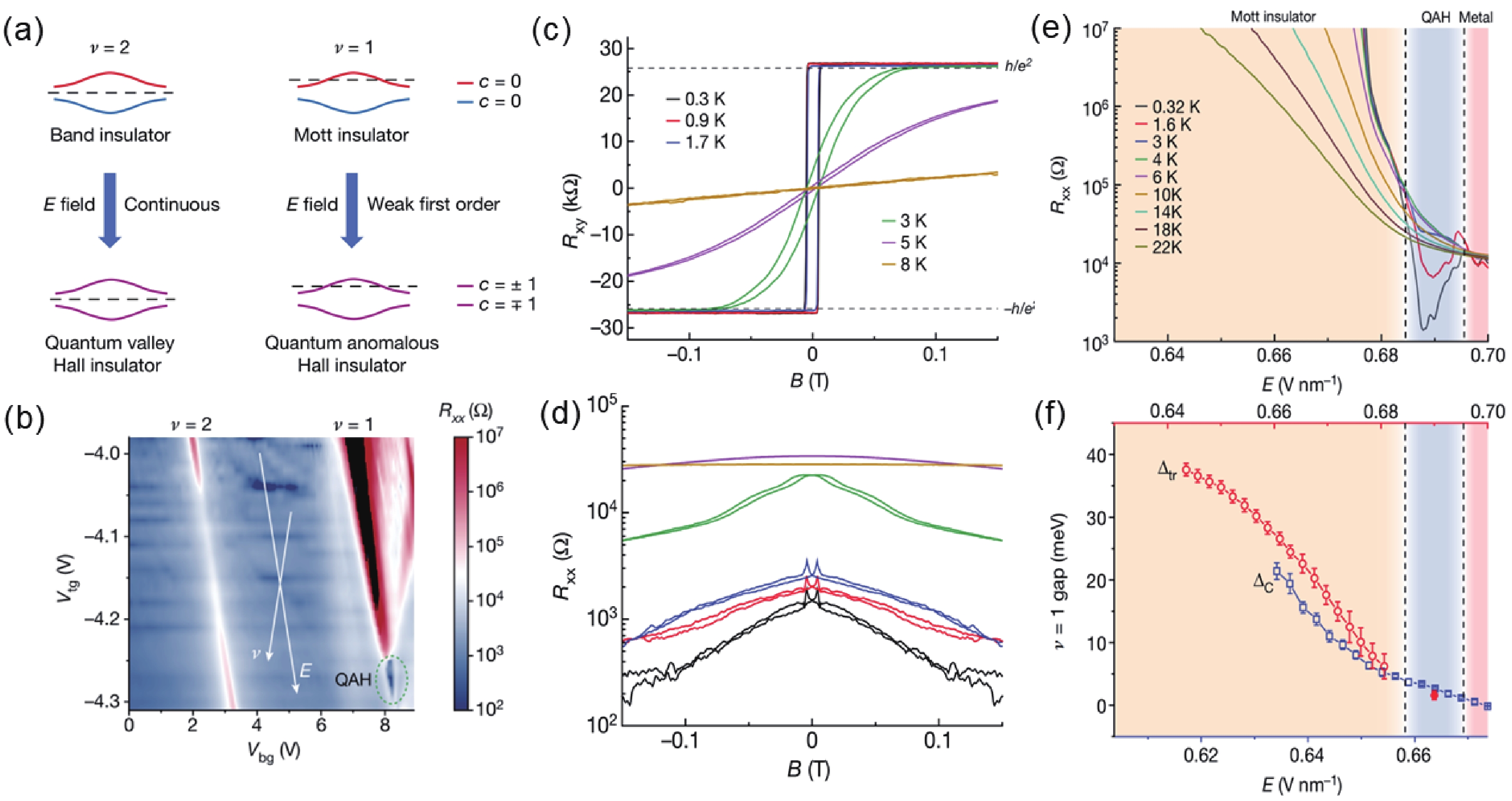
Moiré superlattices are formed when overlaying two materials with a slight mismatch in twist angle or lattice constant. They provide a novel platform for the study of strong electronic correlations and non-trivial band topology, where emergent phenomena such as correlated insulating states, unconventional superconductivity, and quantum anomalous Hall effect are discovered. In this review, we focus on the semiconducting transition metal dichalcogenides (TMDs) based moiré systems that host intriguing flat-band physics. We first review the exfoliation methods of two-dimensional materials and the fabrication technique of their moiré structures. Secondly, we overview the progress of the optically excited moiré excitons, which render the main discovery in the early experiments on TMD moiré systems. We then introduce the formation mechanism of flat bands and their potential in the quantum simulation of the Hubbard model with tunable doping, degeneracies, and correlation strength. Finally, we briefly discuss the challenges and future perspectives of this field.


J. Semicond.
2023, 44(1): 011902 doi: 10.1088/1674-4926/44/1/011902

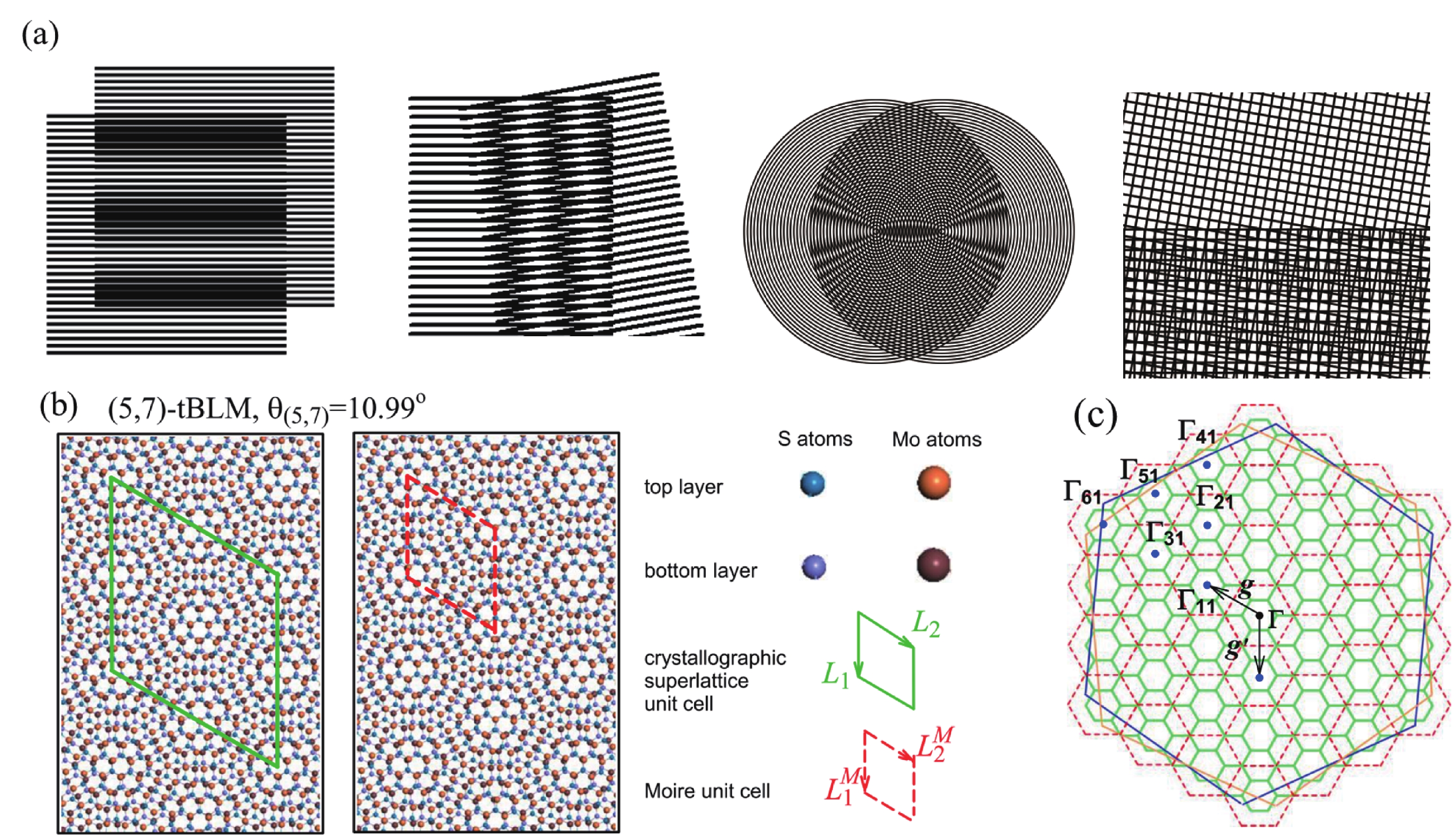
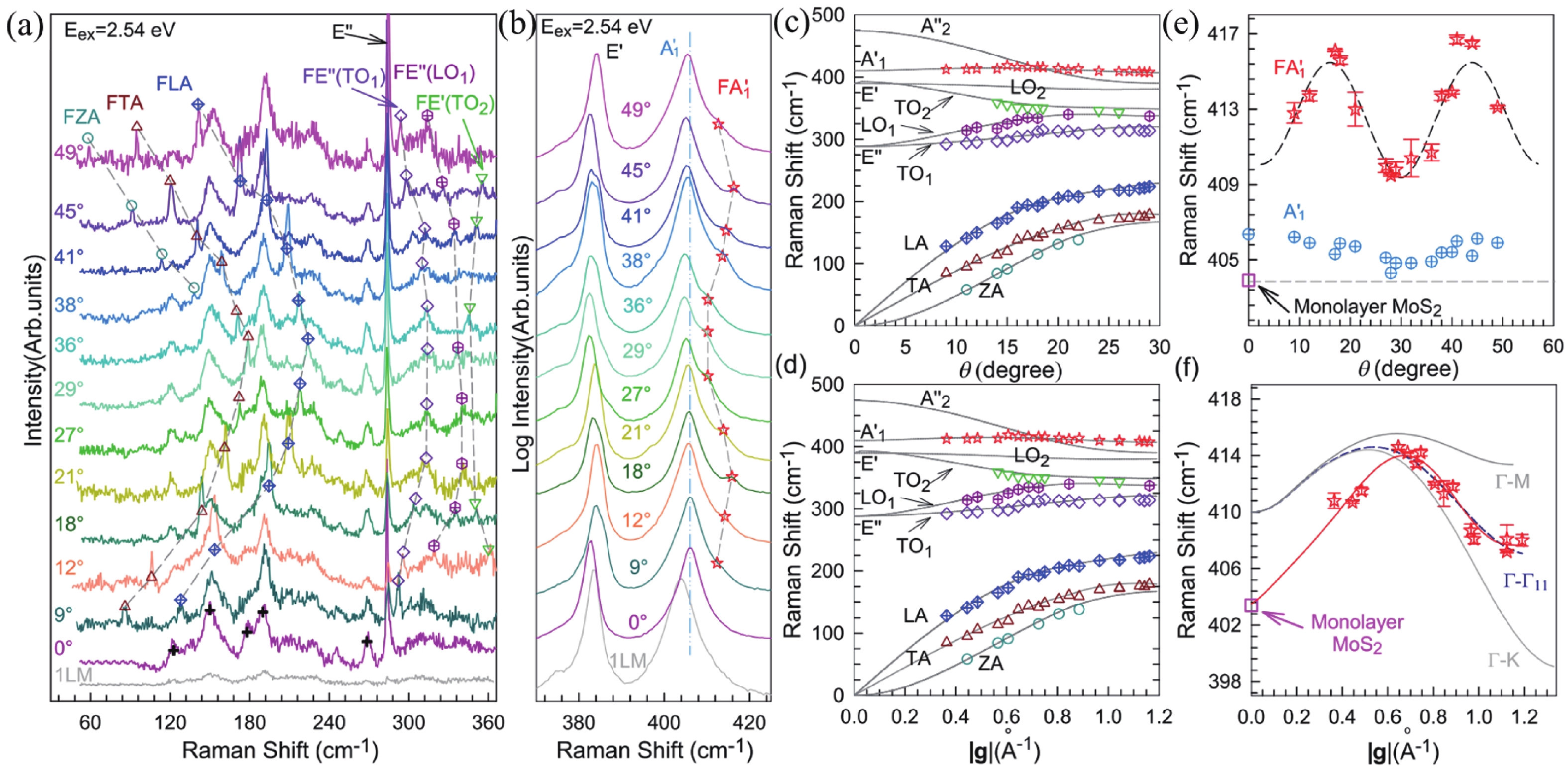
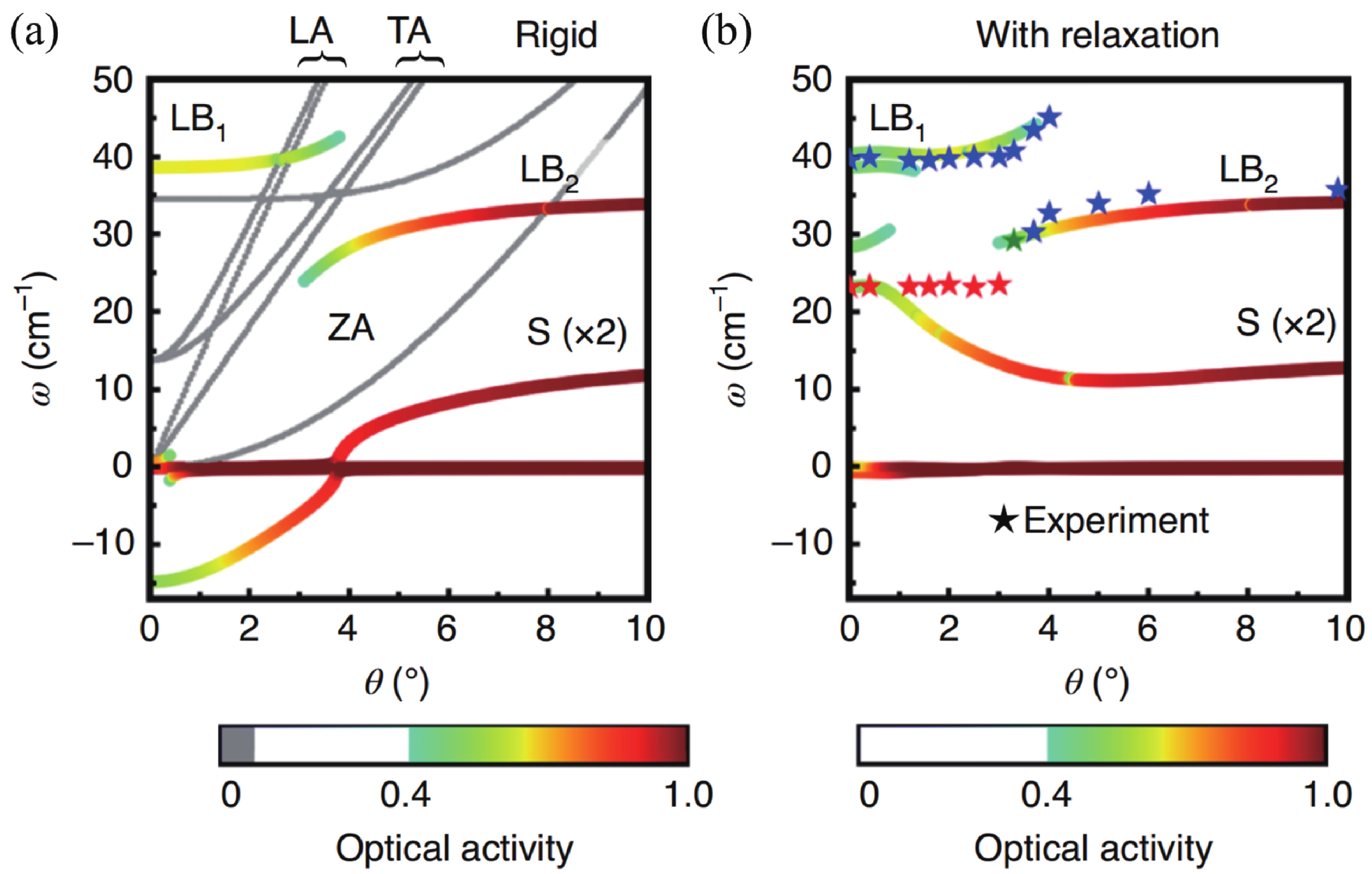
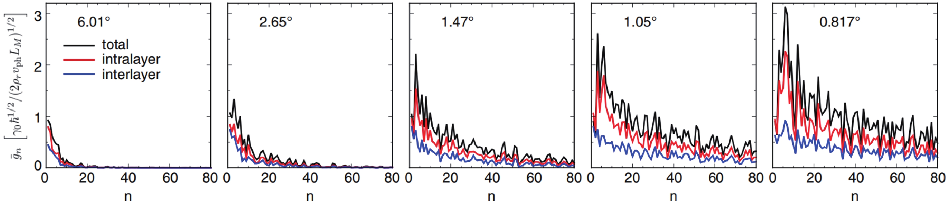
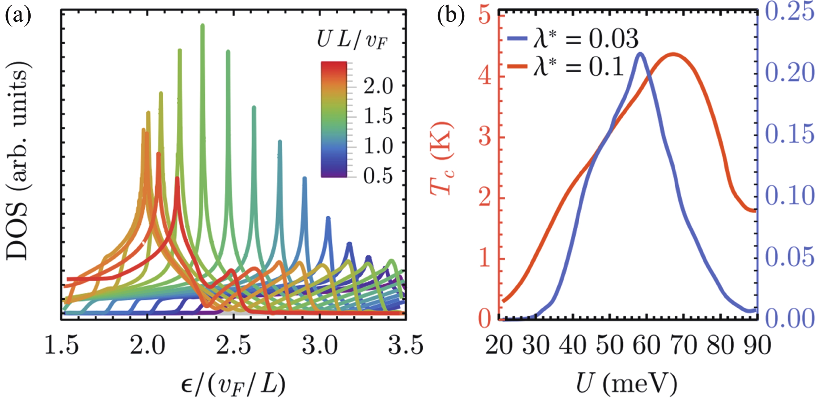
Moiré patterns in physics are interference fringes produced when a periodic template is stacked on another similar one with different displacement and twist angles. The phonon in two-dimensional (2D) material affected by moiré patterns in the lattice shows various novel physical phenomena, such as frequency shift, different linewidth, and mediation to the superconductivity. This review gives a brief overview of phonons in 2D moiré superlattice. First, we introduce the theory of the moiré phonon modes based on a continuum approach using the elastic theory and discuss the effect of the moiré pattern on phonons in 2D materials such as graphene and MoS2. Then, we discuss the electron–phonon coupling (EPC) modulated by moiré patterns, which can be detected by the spectroscopy methods. Furthermore, the phonon-mediated unconventional superconductivity in 2D moiré superlattice is introduced. The theory of phonon-mediated superconductivity in moiré superlattice sets up a general framework, which promises to predict the response of superconductivity to various perturbations, such as disorder, magnetic field, and electric displacement field.


J. Semicond.
2023, 44(1): 011903 doi: 10.1088/1674-4926/44/1/011903

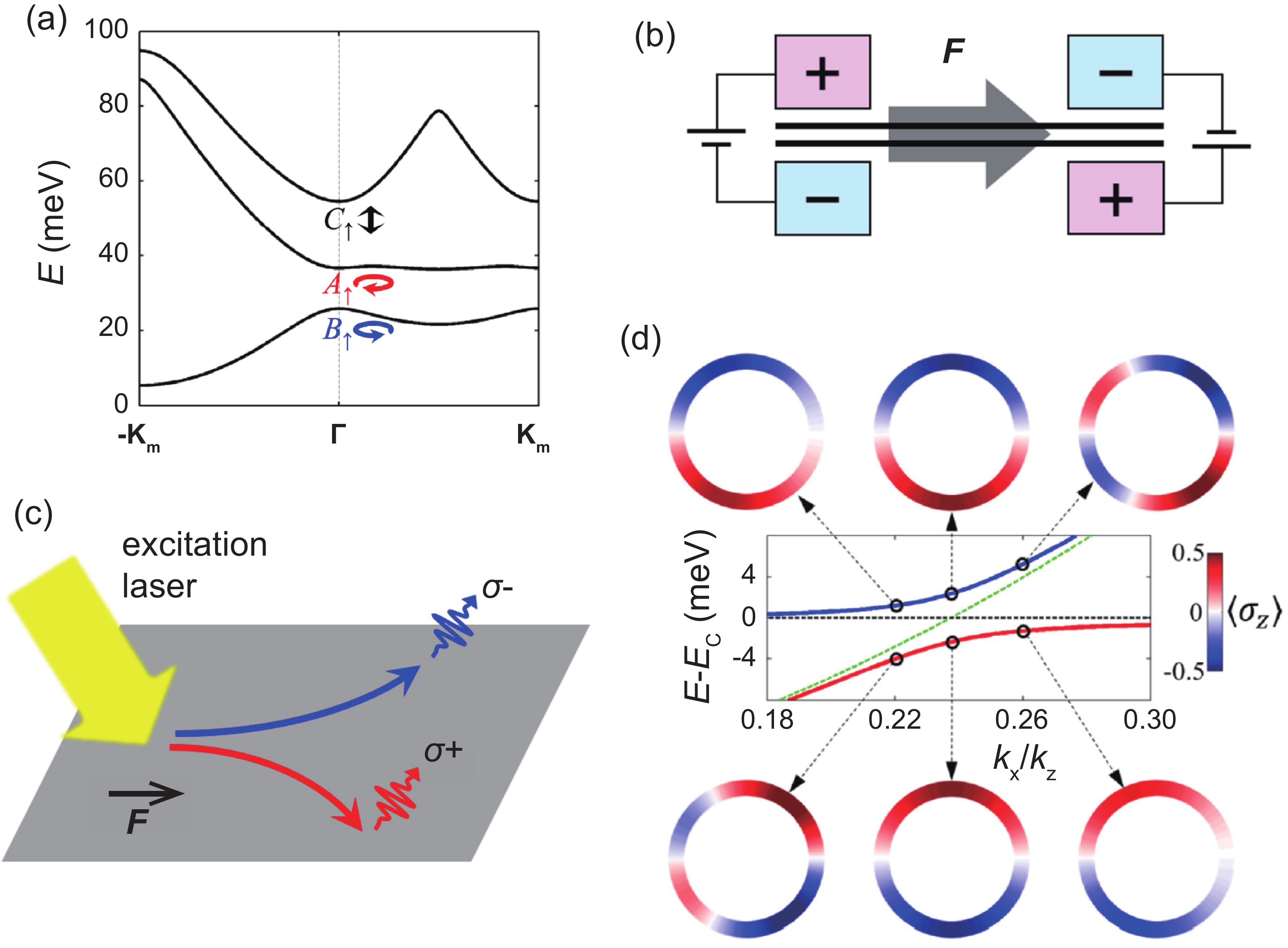
Moiré materials, composed of two single-layer two-dimensional semiconductors, are important because they are good platforms for studying strongly correlated physics. Among them, moiré materials based on transition metal dichalcogenides (TMDs) have been intensively studied. The hetero-bilayer can support moiré interlayer excitons if there is a small twist angle or small lattice constant difference between the TMDs in the hetero-bilayer and form a type-II band alignment. The coupling of moiré interlayer excitons to cavity modes can induce exotic phenomena. Here, we review recent advances in the coupling of moiré interlayer excitons to cavities, and comment on the current difficulties and possible future research directions in this field.


J. Semicond.
2023, 44(1): 012001 doi: 10.1088/1674-4926/44/1/012001
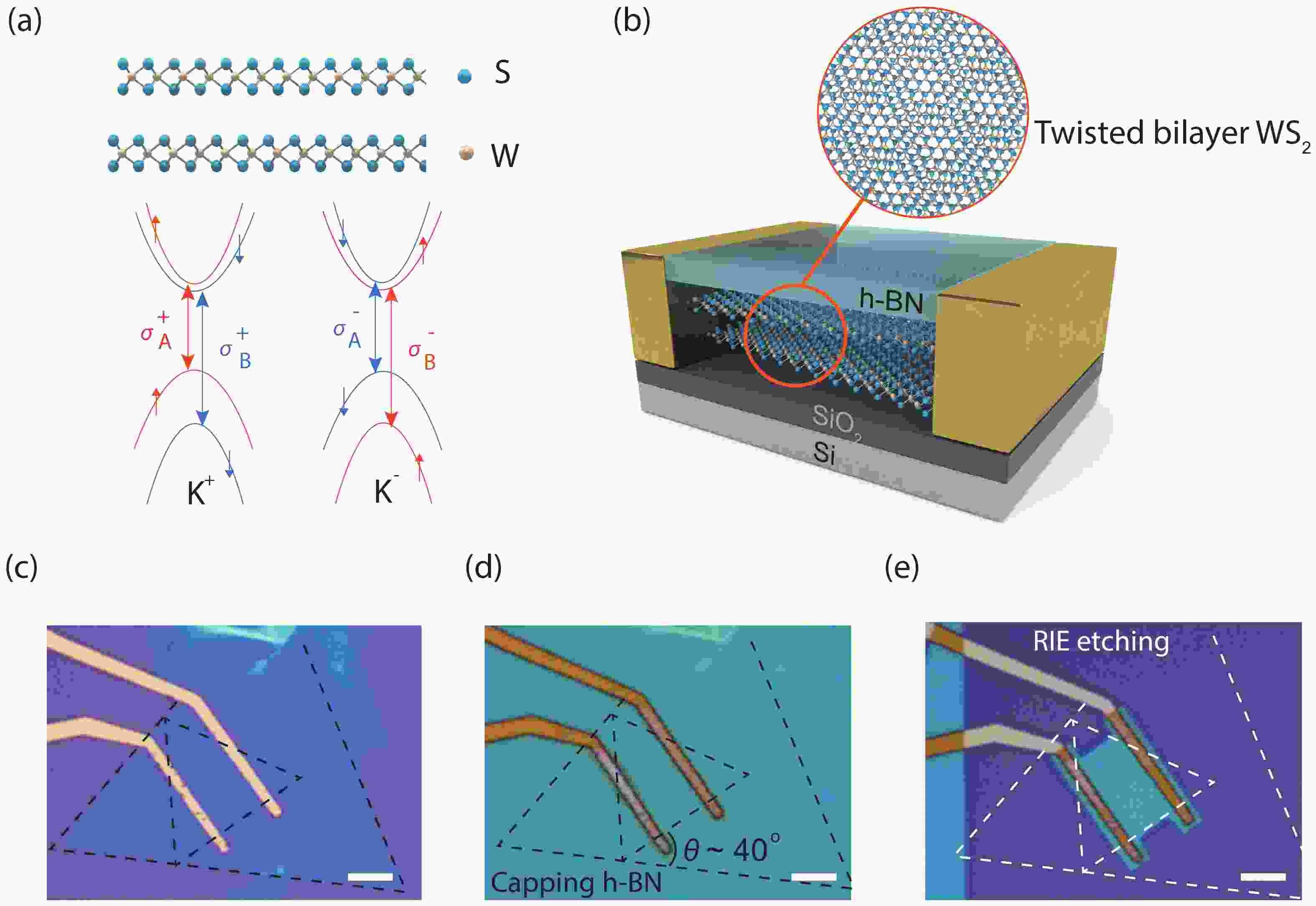
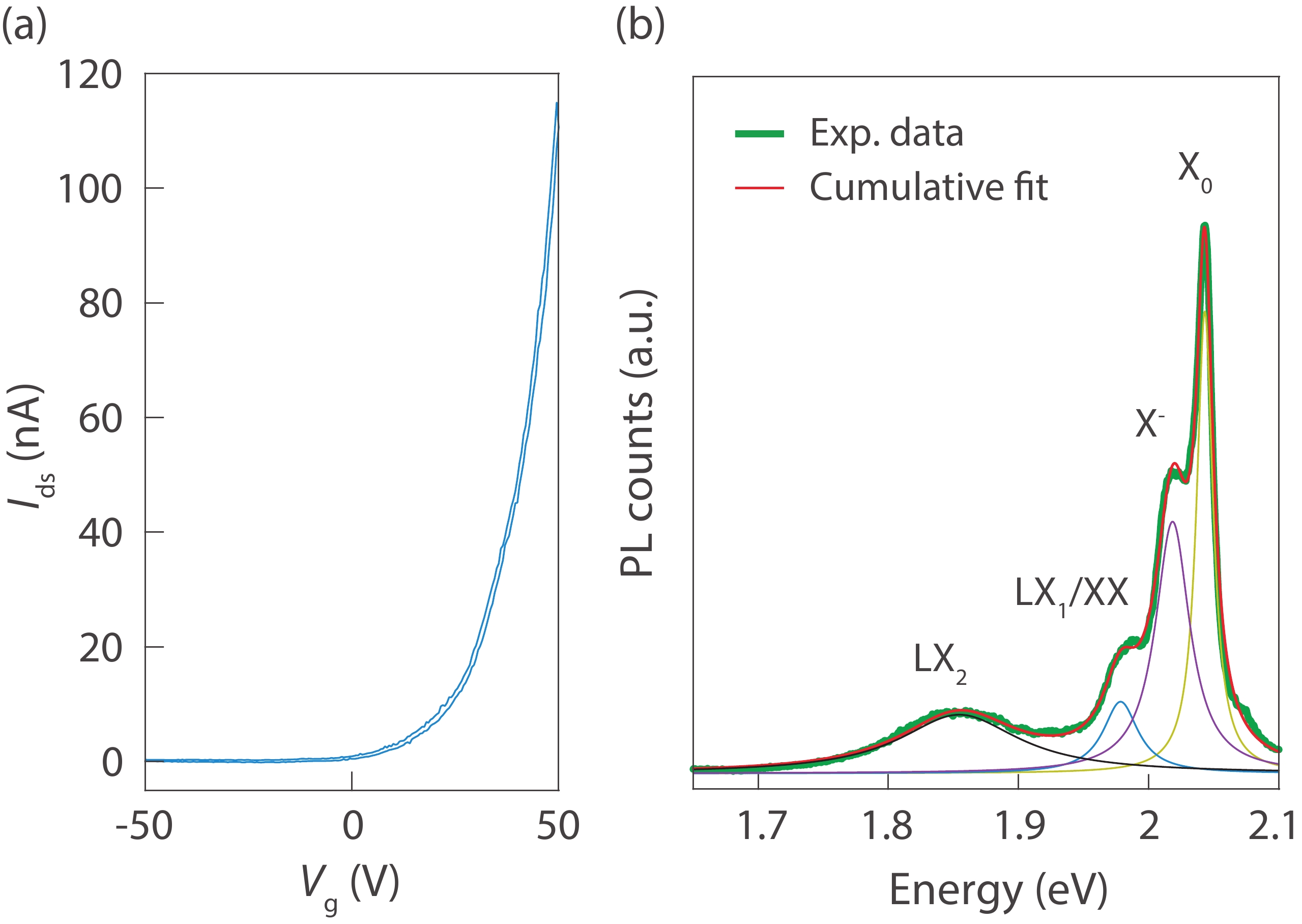
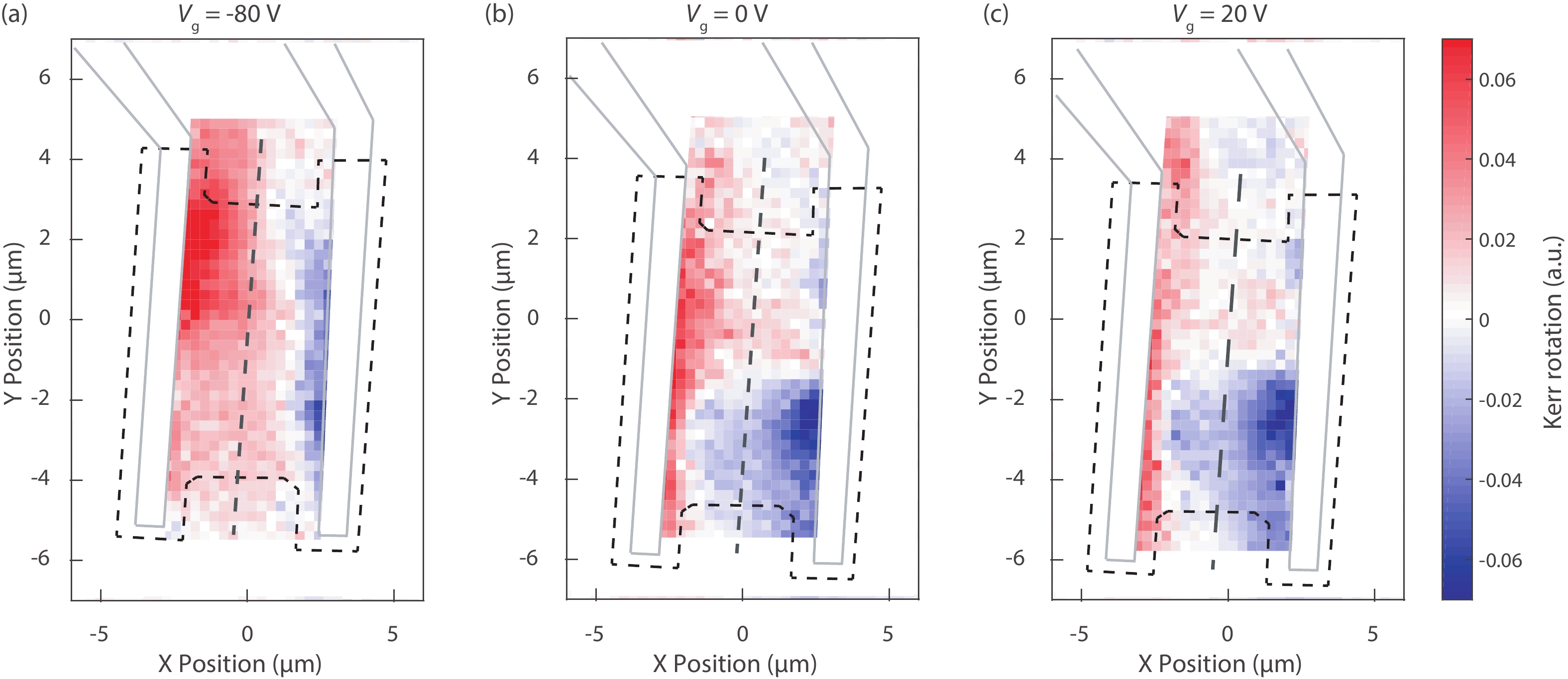
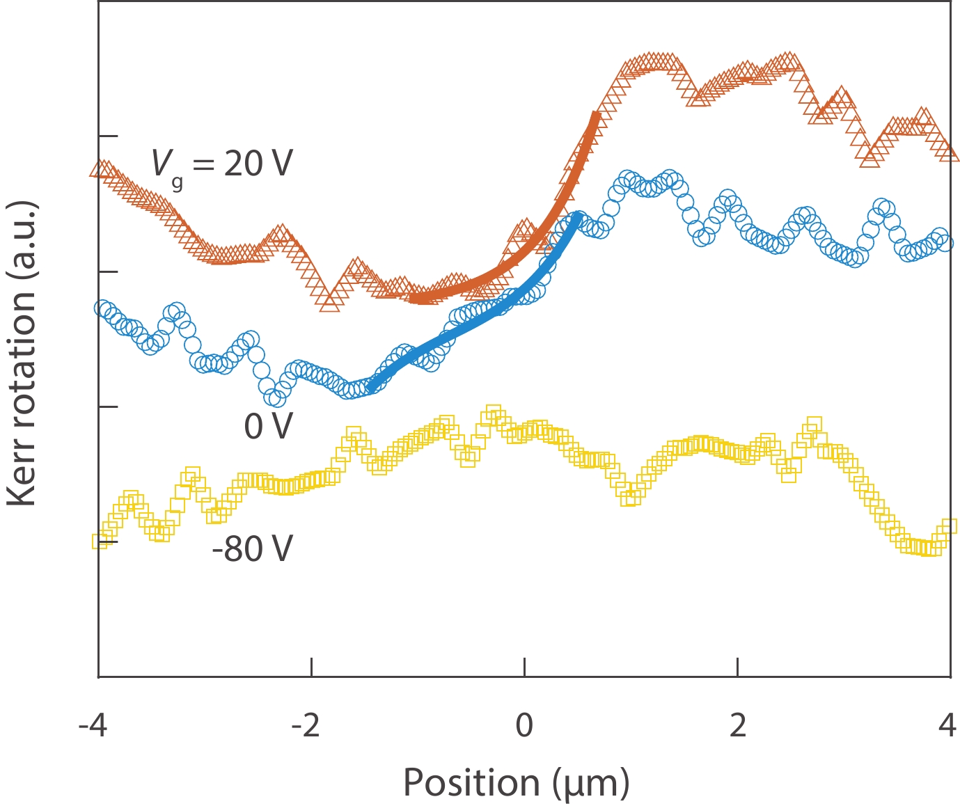
The emerging two-dimensional materials, particularly transition metal dichalcogenides (TMDs), are known to exhibit valley degree of freedom with long valley lifetime, which hold great promises in the implementation of valleytronic devices. Especially, light–valley interactions have attracted attentions in these systems, as the electrical generation of valley magnetization can be readily achieved — a rather different route toward magnetoelectric (ME) effect as compared to that from conventional electron spins. However, so far, the moiré patterns constructed with twisted bilayer TMDs remain largely unexplored in regard of their valley spin polarizations, even though the symmetry might be distinct from the AB stacked bilayer TMDs. Here, we study the valley Hall effect (VHE) in 40°-twisted chemical vapor deposition (CVD) grown WS2 moiré transistors, using optical Kerr rotation measurements at 20 K. We observe a clear gate tunable spatial distribution of the valley carrier imbalance induced by the VHE when a current is exerted in the system.

J. Semicond.
2023, 44(1): 012301 doi: 10.1088/1674-4926/44/1/012301
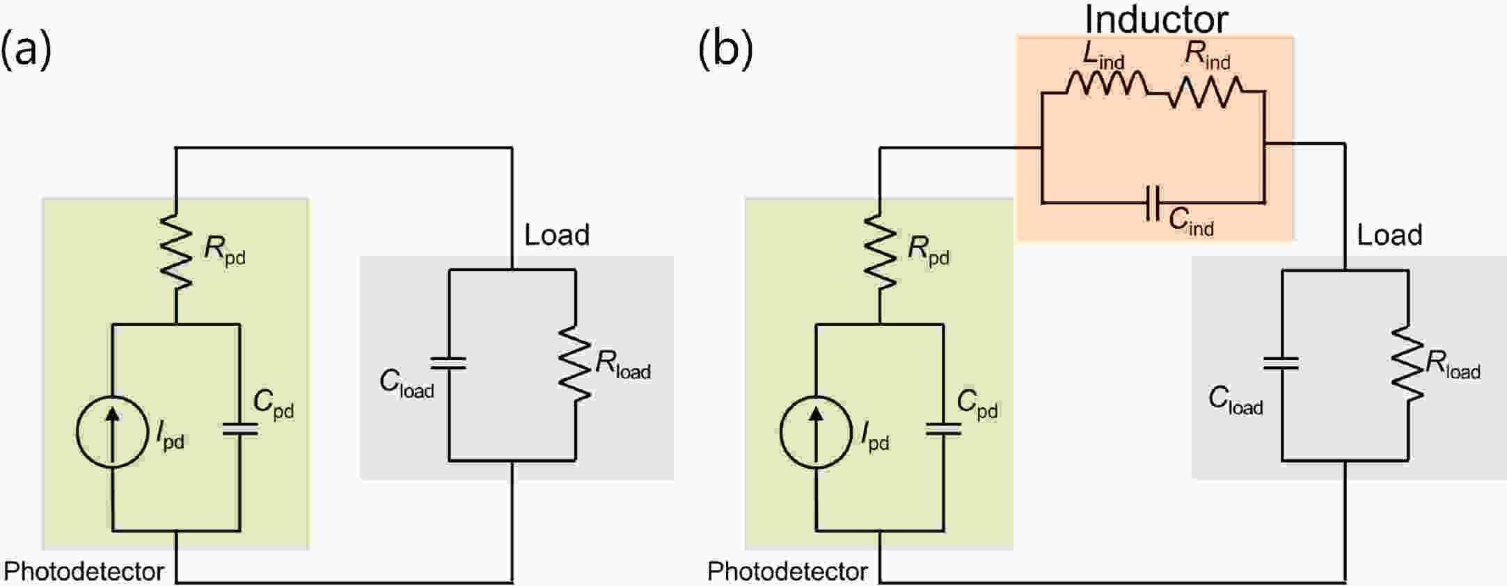
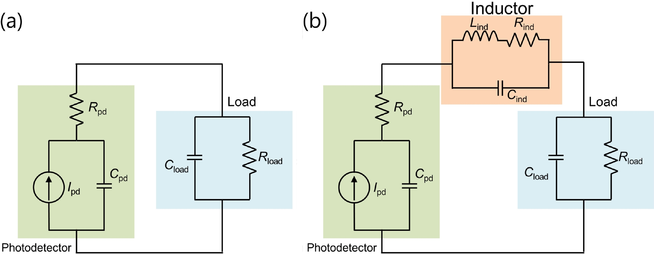
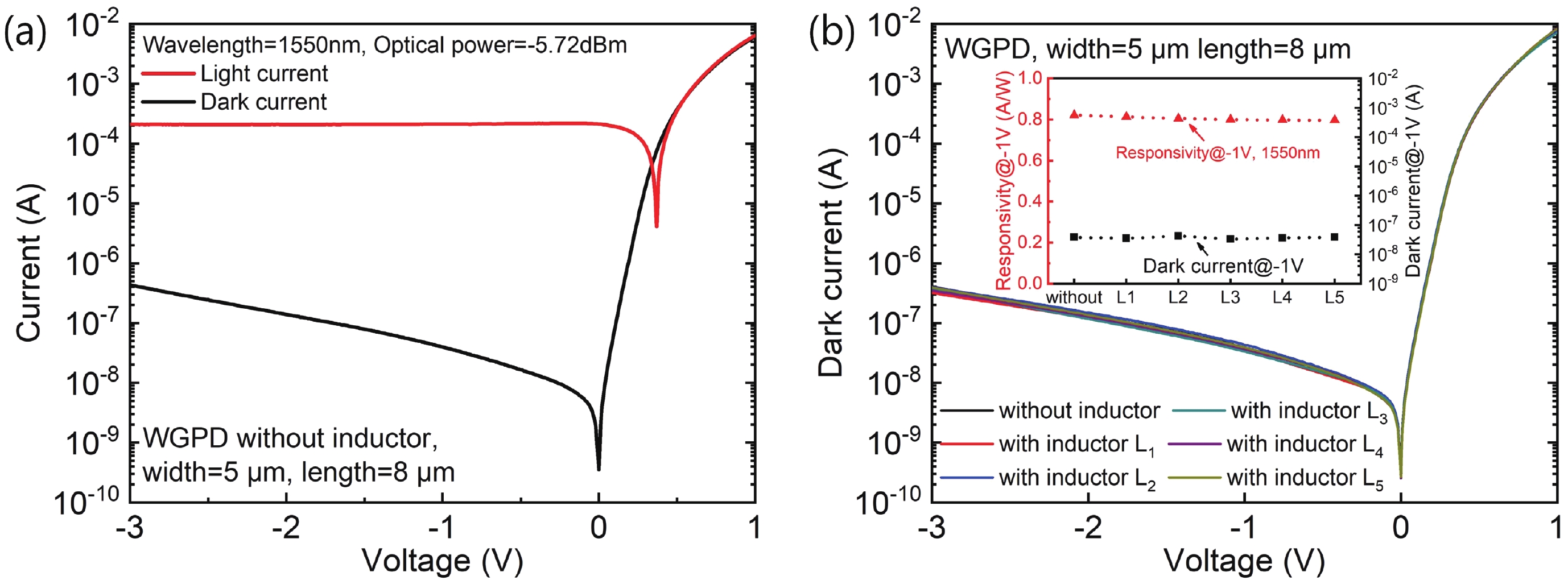
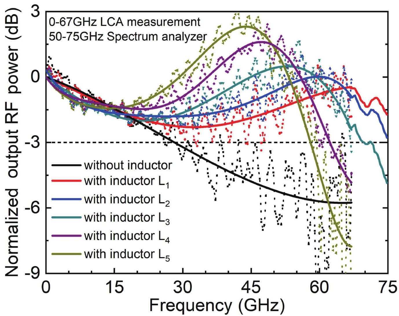
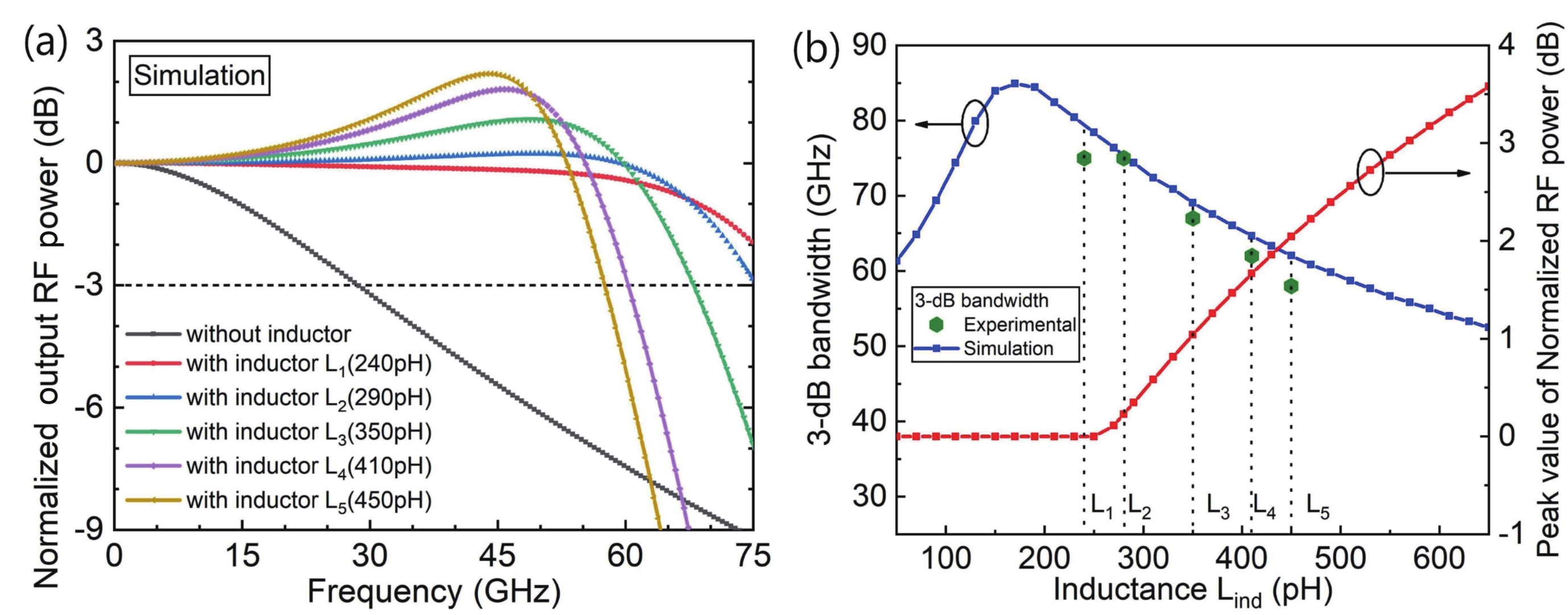
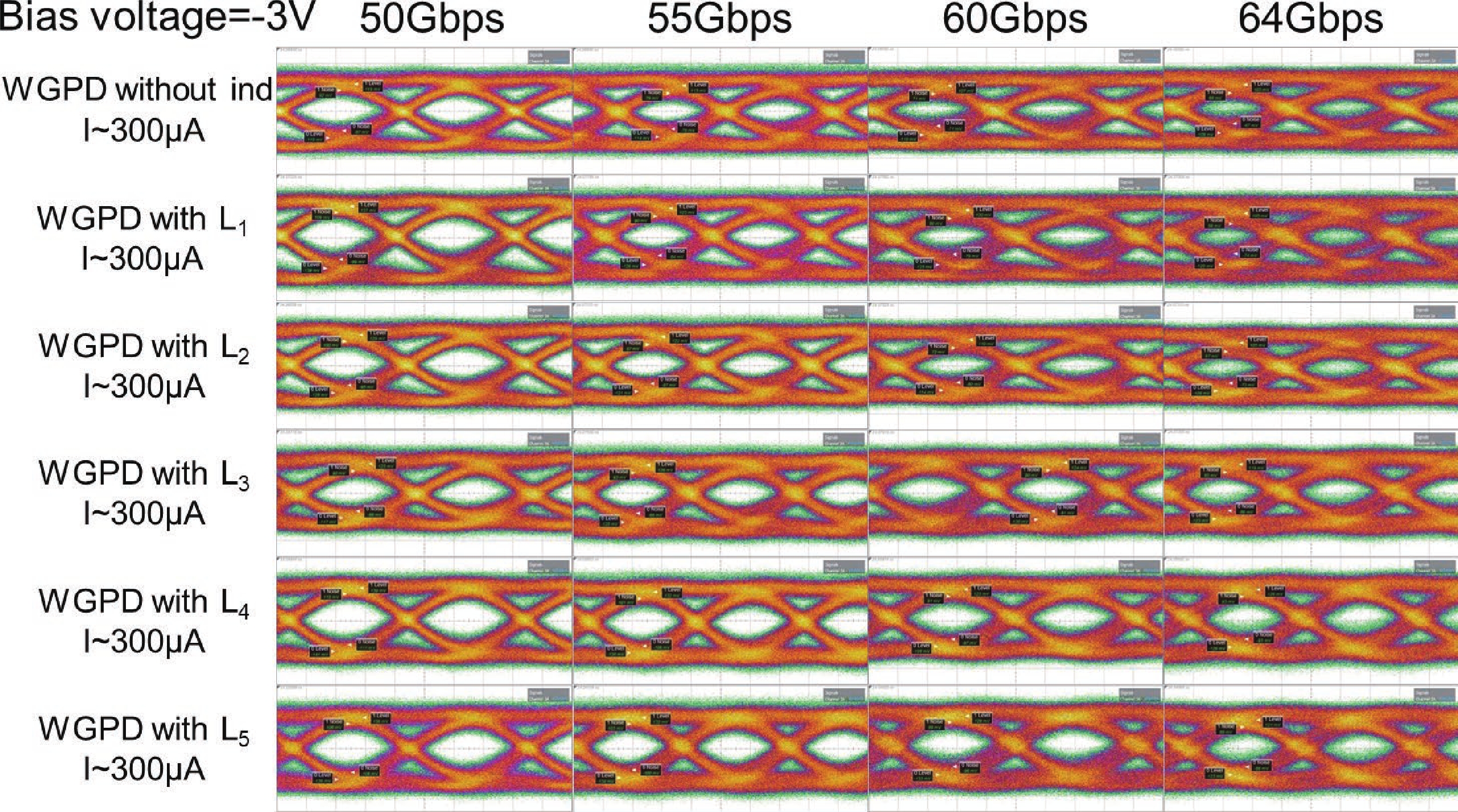
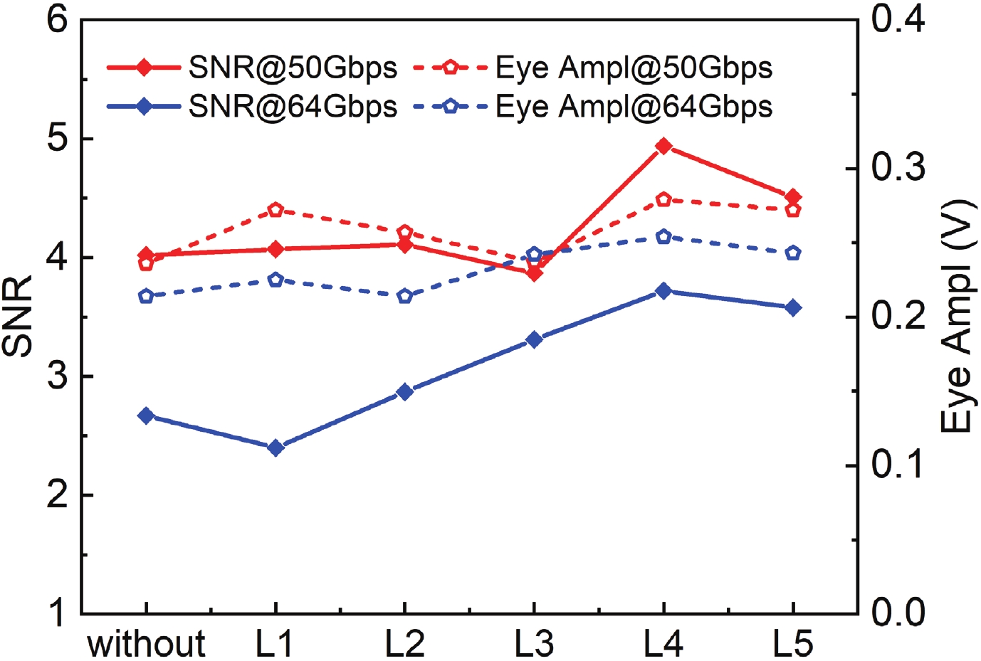
High-performance germanium (Ge) waveguide photodetectors are designed and fabricated utilizing the inductive-gain-peaking technique. With the appropriate integrated inductors, the 3-dB bandwidth of photodetectors is significantly improved owing to the inductive-gain-peaking effect without any compromises to the dark current and optical responsivity. Measured 3-dB bandwidth up to 75 GHz is realized and clear open eye diagrams at 64 Gbps are observed. In this work, the relationship between the frequency response and large signal transmission characteristics on the integrated inductors of Ge waveguide photodetectors is investigated, which indicates the high-speed performance of photodetectors using the inductive-gain-peaking technique.


J. Semicond.
2023, 44(1): 012701 doi: 10.1088/1674-4926/44/1/012701
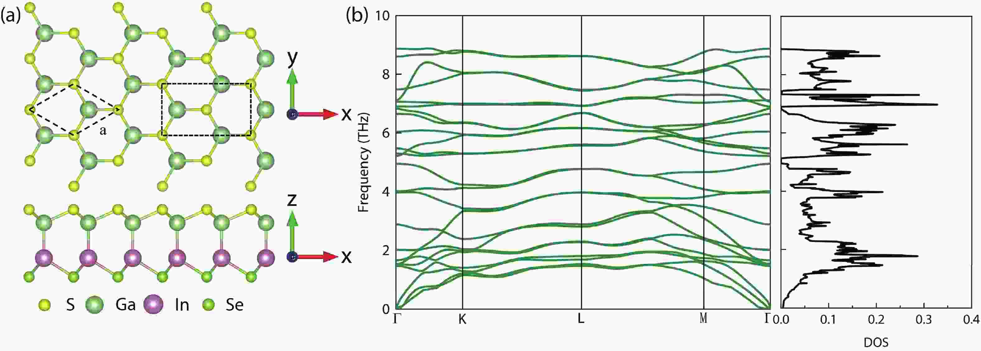
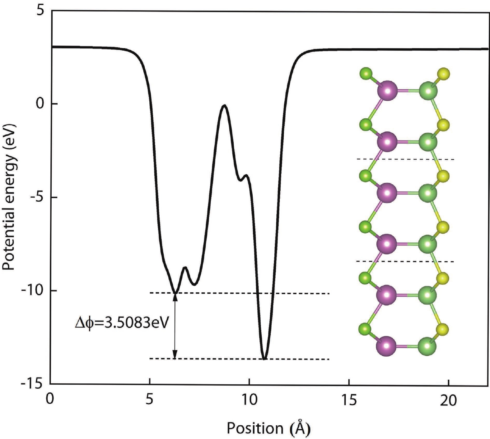
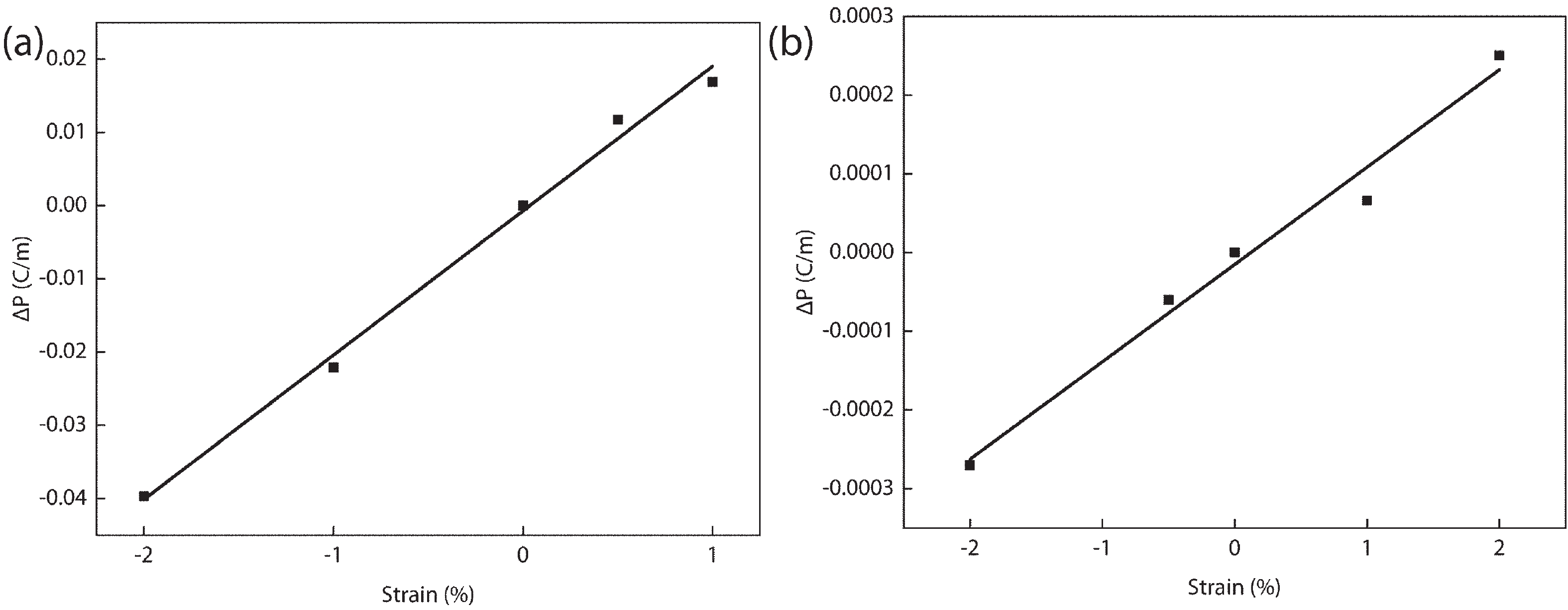
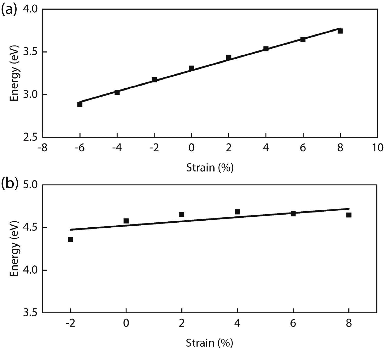
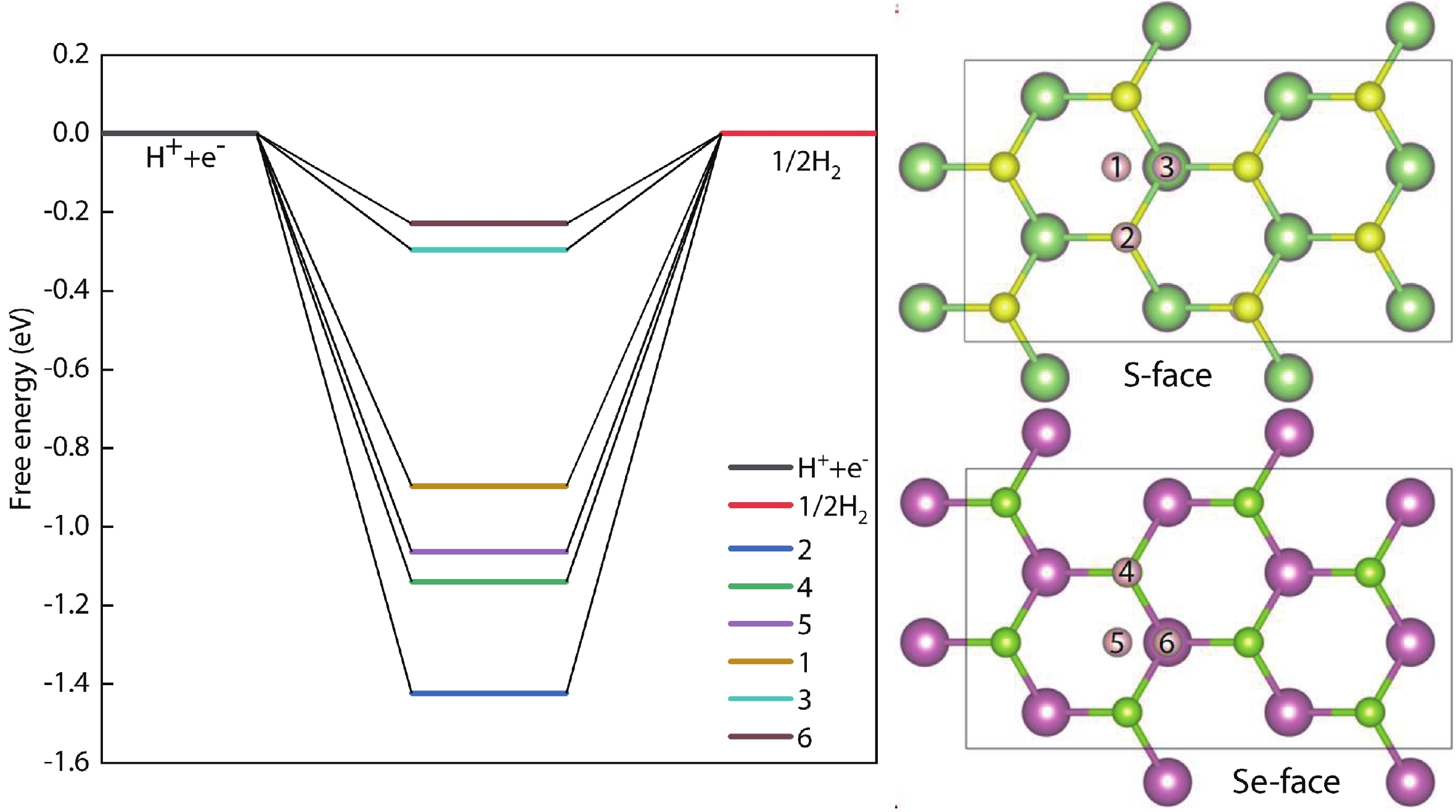
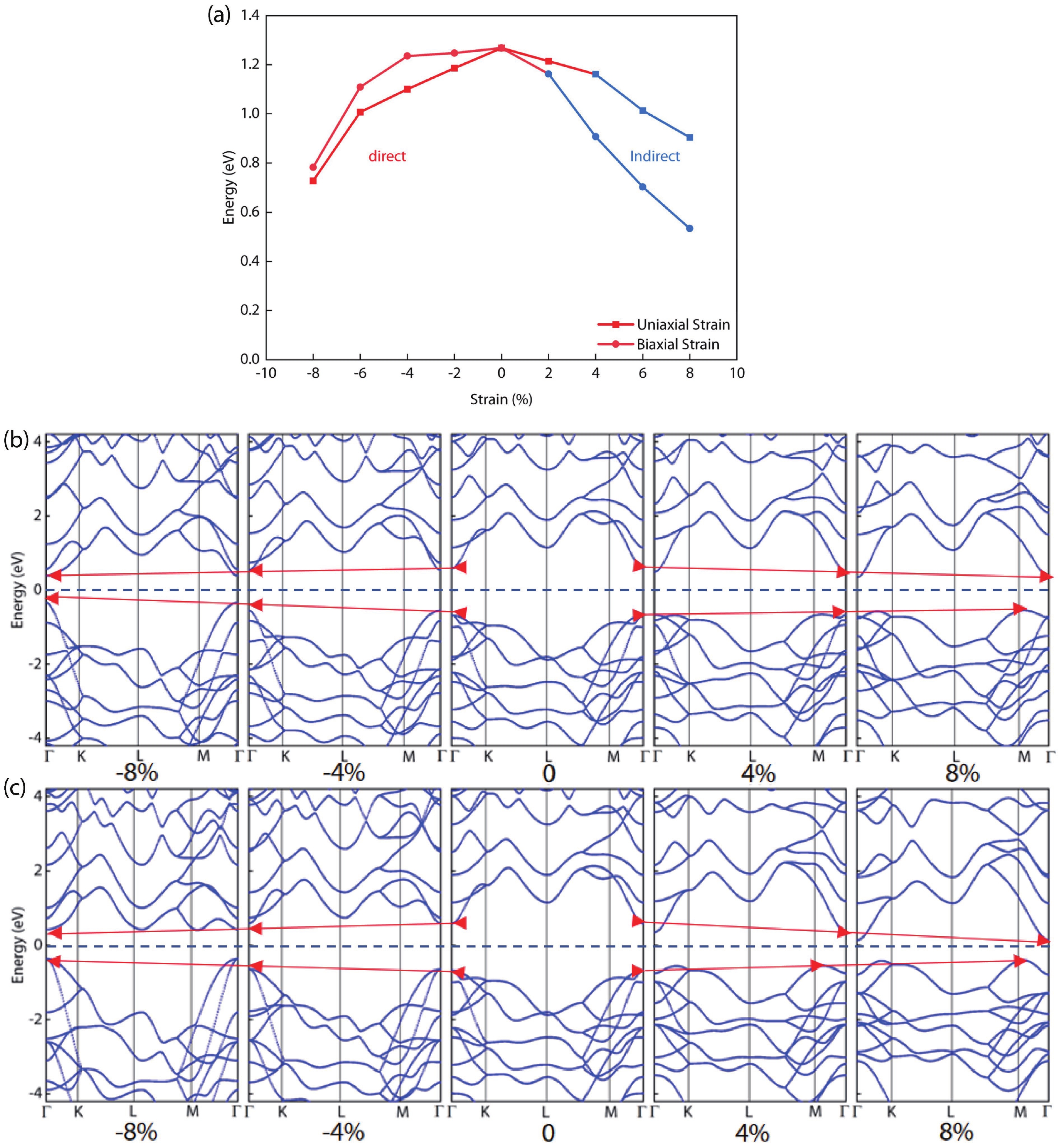
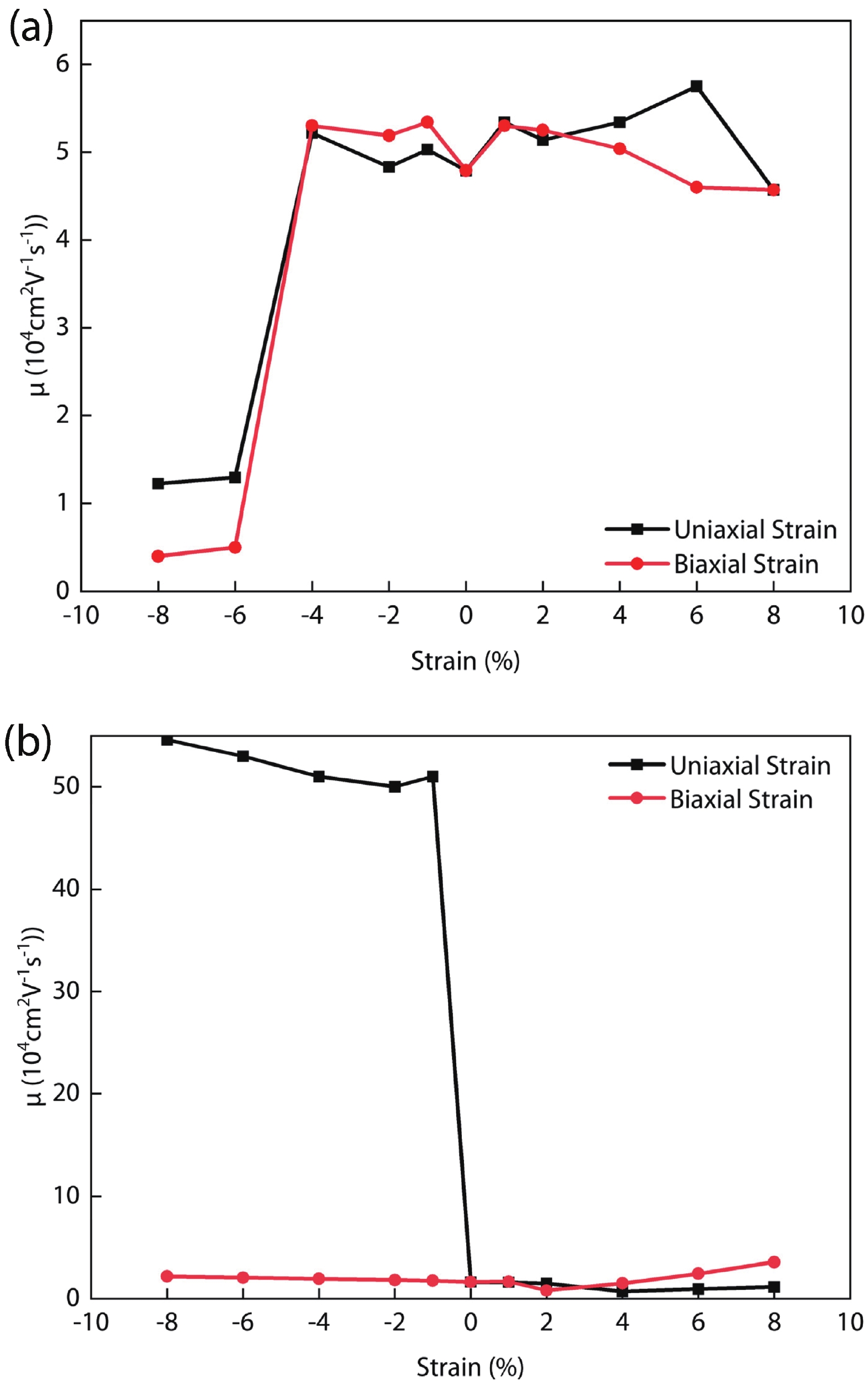
In recent years, Janus two-dimensional (2D) materials have received extensive research interests because of their outstanding electronic, mechanical, electromechanical, and optoelectronic properties. In this work, we explore the structural, electromechanical, and optoelectronic properties of a novel hypothesized Janus InGaSSe monolayer by means of first-principles calculations. It is confirmed that the Janus InGaSSe monolayer indeed show extraordinary charge transport properties with intrinsic electron mobility of 48 139 cm2/(V·s) and hole mobility of 16 311 cm2/(V·s). Both uniaxial and biaxial strains can effectively tune its electronic property. Moreover, the Janus InGaSSe monolayer possesses excellent piezoelectric property along both in-plane and out-of-plane directions. The results of this work imply that the Janus InGaSSe monolayer is in fact an efficient photocatalyst candidate, and may provide useful guidelines for the discovery of other new 2D photocatalytic and piezoelectric materials.